

Page 1

DVD Player
HTS5500C/37/55
CLASS 1
LASER PRODUCT
1 Technical Specifi cations and Connection
Facilities 2
Location of PC Boards 2
Technical Specifi cations 3
Measurement Setup 4
Service Aids 5
Lead Free Requirements 7
2 Dismantling instructions & Service Positions 8
Dismantling instructions 8
3 Diagnostic Software 10
Service test program 10
4 Set Block diagram 13
5 Set wiring diagram 14
6 Panel Front Boards 15
Front Display - Component Layout 15
Front Display - Chip Layout 15
Front Display - Circuit Diagram 16
Key & Open/close Board - Component Layout 17
Key & Open/close Board - Chip Layout 17
Key & Open/close Board - Circuit Diagram 18
Front key board - Component Layout 19
Front key board - Chip Layout 19
Front key board - Circuit Diagram 20
Video Connector Board - Circuit Diagram 21
Video Connector Board - Component Layout 22
Video Connector Board - Chip Layout 22
7 AV Board 23
AV Board - Top view layout 23
©
Copyright 2005 Philips Consumer Electronics B.V. Eindhoven, The Netherlands.
All rights reserved. No part of this publication may be reproduced, stored in
a retrieval system or transmitted, in any form or by any means, electronic,
mechanical, photocopying, or otherwise without the prior permission of Philips.
Contents PageContents Page
AV Board - Bottom view layout 24
AV Board - Circuit Diagram (Part 1) 25
AV Board - Circuit Diagram (Part 2) 26
AV Board - Circuit Diagram (Part 3) 27
AV Board - Circuit Diagram (Part 4) 28
AV Board - Circuit Diagram (Part 5) 29
AV Board - Circuit Diagram (Part 6) 30
8 Powerbox Spk Assy SW5500C 31
Power Supply Unit - Top view layout 31
Power Supply Unit - Circuit Diagram (Part 1) 32
Power Supply Unit - Circuit Diagram (Part 2) 33
Interface - Top view layout 34
Interface - Circuit Diagram (Part 1) 35
Main Amplifer - Top view layout 36
Main Amplifer - Bottom view layout 37
Connector schematic 38
FR+SURROUND amplifi er schematic 39
Subwoofer Amplifer - Top view layout 40
Subwoofer Amplifer - Bottom view layout 41
Subwoofer amplifi er schematic 42
Transformer - Top silk layout 43
Exploded View - Box Spk Assy SW5500C 44
Exploded View - Module 45
Wiring Diagram SW5500C 46
9 Module SD6.3 CH HT 47
SD6.3 CH HT Board - Top View Layout 47
SD6.3 CH HT Board - Bottom View Layout 48
SD6.3 CH HT Board - Circuit Diagram (Part1) 49
SD6.3 CH HT Board - Circuit Diagram (Part2) 50
10 Set Mechanical Exploded View 51
11 Partlist 53
Published by KC-TE 0519 AV Systems Printed in the Netherlands Subject to modifi cation EN 3139 785 31200
Version 1.0
Page 2
EN 2
HTS5500C/37/551.
Technical Specifi
cations and Connection Facilities
1. Technical Specifi cations and Connection Facilities
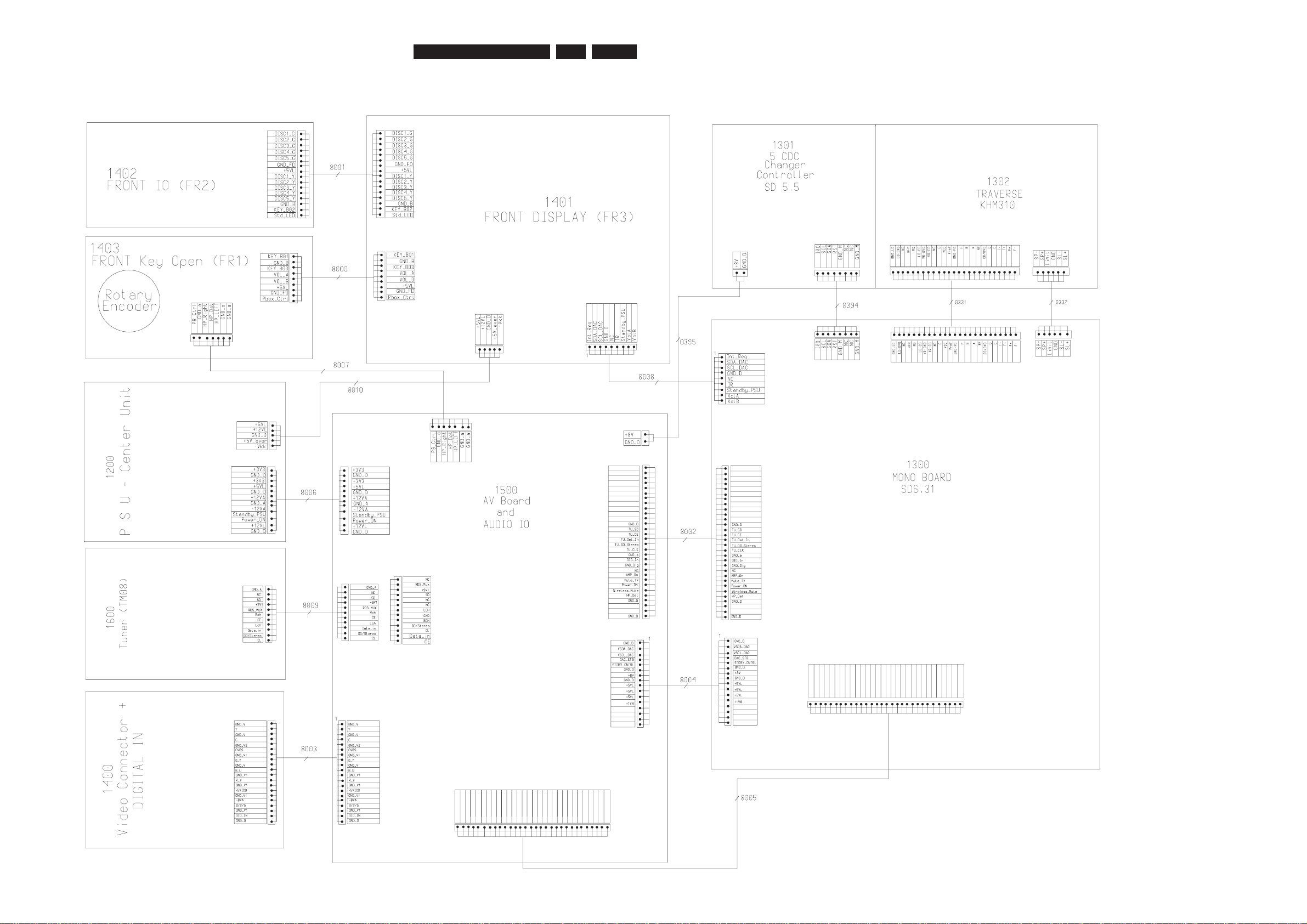
LOCATION OF PC BOARDS
HTS5500 Architecture
PSU
Board
5-DISC
CHANGER
MECHANISM
AV-BOARD-2
TUNER TM08
AV-BOARD -1
SD 6.3
FRONT BOARD
3 PIECES
VERSION VARIATIONS:
Features &
Board in used:
Progressive Scan X X
Control Line To Power Box X X
Audio Output X X
Audio Input X X
Power Box (Easy Fit) X X
Video Output X X
S-Video Output X X
Y/Pb/Pr (YUV) Component Video Output X X
Type / Versions:
37 55
HTS5500C
Page 3

Technical Specifi
cations and Connection Facilities
Technical Specifi cations
HTS5500C/37/55
1.
EN 3
General:
Mains voltage : 120V ± 15%
240V ± 15%
Mains frequency : 50/60Hz
Power consumption : <= 0.5W at standby
(Center Unit)
<= 0.5W at standby
(Subwoofer)
<= 25W at 1/8 P
rated
(Center Unit)
Dimension (w x h x d) : 360 x 40 x 305mm
Tuner
FM
Tuning range : 87.5-108MHz
Grid : 50kHz /01
100kHz /97
IF frequency : 10.7MHz ± 25kHz
Aerial input : 75Ω coaxial
Sensitivity at 26dB S/N : < 7μV
Selectivity at 600kHz bandwidth : > 25dB
IF rejection : > 60dB
Image rejection : > 25dB
Distortion at RF=1mV, dev. 75kHz : < 3%
-3dB Limiting point : 8μV
Crosstalk at RF=1mV, dev. 67.5kHz : > 28dB
Crosstalk at RF=1mV, dev. 40kHz : > 18dB /97
MW
Input sensitivity
Aux In : 1V at 39kΩ
Scart In : 500mV at 39kΩ
Output sensitivity
Line Out (Left/Right) : 0.7V ± 2dB at 47kΩ
Scart Out (Left/Right) : 0.6V ± 2dB at 10kΩ
COMPACT DISC/VCD/DVD:
Video Decoding : MPEG-1/MPEG-2/
MPEG-4/DivX 3.11,
4.x & 5.x
Video DAC : 12 Bits, 108MHz
Signal System : PAL / NTSC
Video Format : 4:3 / 16:9
Video S/N : 56dB (minimum)
CVBS Out
CVBS level : 1.0 ± 0.1V
Luminance S/N : >= 55dB
S-Video Out
Y level : 1.0 ± 0.1V
Y S/N : >= 60dB
C level (burst) : 286mV
RGB/YUV Out
Amplitude : 0.7 ± 0.1V
S/N : >= 60dB
1)
1)
1)
p-p
p-p
+1/-4dB
p-p
p-p
Tuning range : 531-1602kHz
530-1700kHz for /97
Grid : 9kHz
10kHz /97
IF frequency : 450kHz ± 1kHz
Aerial input : Frame aerial
Sensitivity at 26dB S/N : < 4.0mV/m
Selectivity at 18kHz bandwidth : > 20dB
IF rejection : > 45dB
Image rejection : > 28dB
Distortion at RF=50mV, m=80% : < 5%
AMPLIFIER:
Output power : 900W RMS
Front : 150W RMS / channel
Rear : 150W RMS / channel
Centre : 150W RMS
Subwoofer : 150W RMS
Frequency response : 20Hz-50kHz / -3dB
Signal-to-noise ratio : > 65dB (CCIR)
1)
Output terminals to be terminated with 75Ω
2)
@ THD = 10%, 1kHz Sinewave except Subwoofer
@ 100Hz Sinewave
Page 4
EN 4
1.
HTS5500C/37/55
MEASUREMENT SETUP
Tuner FM
Technical Specifi
cations and Connection Facilities
Bandpass
LF Voltmeter
e.g. PM2534
RF Generator
e.g. PM5326
DUT
250Hz-15kHz
e.g. 7122 707 48001
Ri=50Ω
S/N and distortion meter
e.g. Sound Technology ST1700B
Use a bandpass filter to eliminate hum (50Hz, 100Hz) and disturbance from the pilottone (19kHz, 38kHz).
Tuner AM (MW,LW)
RF Generator
e.g. PM5326
Ri=50Ω
DUT
Frame aerial
e.g. 7122 707 89001
Bandpass
250Hz-15kHz
e.g. 7122 707 48001
LF Voltmeter
e.g. PM2534
S/N and distortion meter
e.g. Sound Technology ST1700B
To avoid atmospheric interference all AM-measurements have to be carried out in a Faraday´s cage.
Use a bandpass filter (or at least a high pass filter with 250Hz) to eliminate hum (50Hz, 100Hz).
CD
Use Audio Signal Disc
(replaces test disc 3)
DUT
L
R
SBC429 4822 397 30184
S/N and distortion meter
e.g. Sound Technology ST1700B
LEVEL METER
e.g. Sennheiser UPM550
with FF-filter
Recorder
Use Universal Test Cassette CrO2 SBC419 4822 397 30069
or Universal Test Cassette
LF Generator
e.g. PM5110
Fe SBC420 4822 397 30071
DUT
L
R
S/N and distortion meter
e.g. Sound Technology ST1700B
LEVEL METER
e.g. Sennheiser UPM550
with FF-filter
Page 5
Technical Specifi
cations and Connection Facilities
SERVICE AIDS
Service Tools:
Universal Torx driver holder .................................. 4822 395 91019
Torx bit T10 150mm ............................................. 4822 395 50456
Torx driver set T6 - T20 ......................................... 4822 395 50145
Torx driver T10 extended ...................................... 4822 395 50423
Compact Disc:
SBC426/426A Test disc 5 + 5A ............................ 4822 397 30096
SBC442 Audio Burn-in Test disc 1kHz ................. 4822 397 30155
SBC429 Audio Signals disc .................................. 4822 397 30184
Dolby Pro-logic Test Disc ...................................... 4822 395 10216
HTS5500C/37/55
1.
EN 5
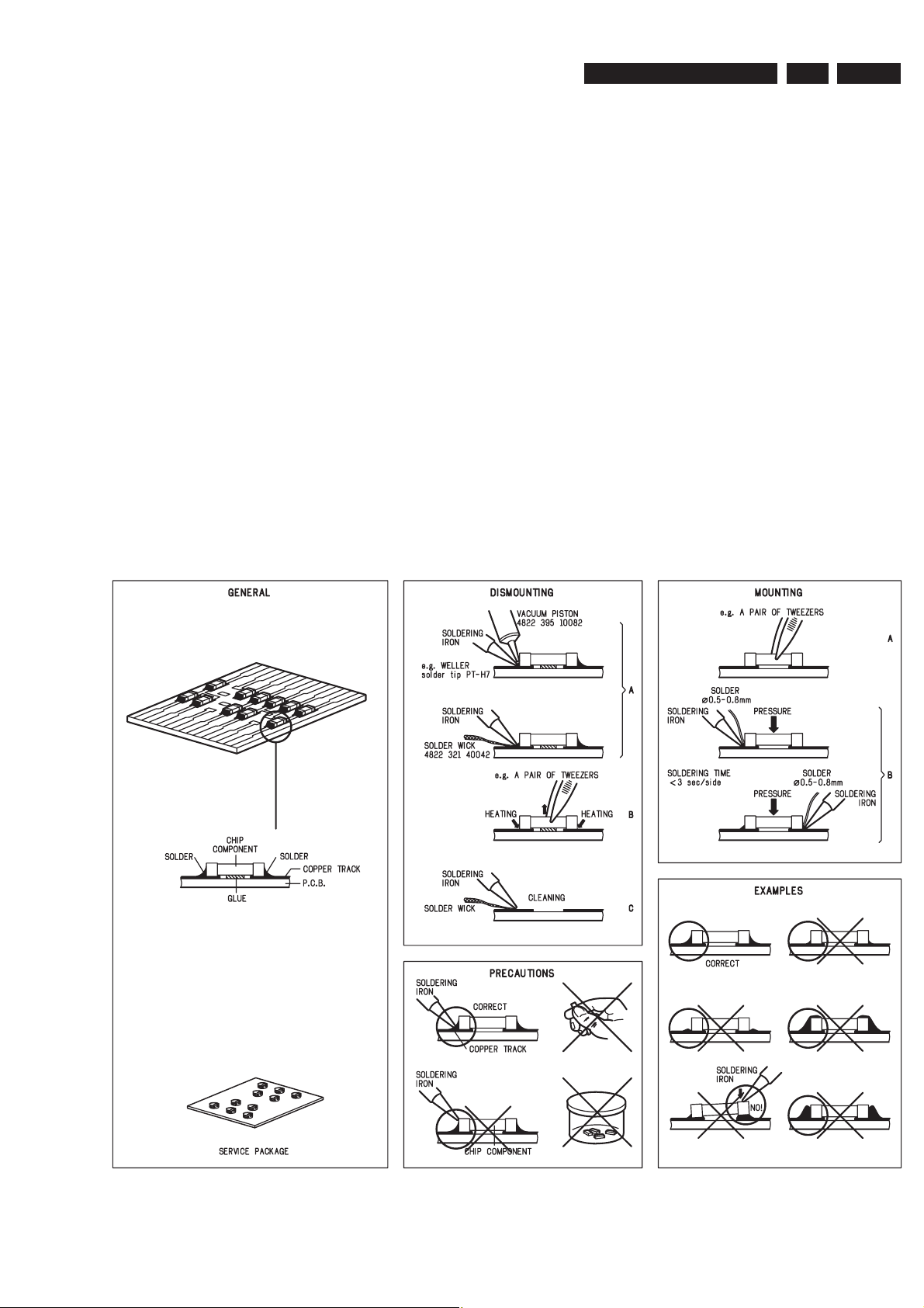
HANDLING CHIP COMPONENTS
Page 6
EN 6
HTS5500C/37/551.
Technical Specifi cations and Connection Facilities
GB
All ICs and many other semi-conductors are
susceptible to electrostatic discharges (ESD).
Careless handling during repair can reduce life
drastically.
When repairing, make sure that you are
connected with the same potential as the mass
of the set via a wrist wrap with resistance.
Keep components and tools also at this
potential.
Tous les IC et beaucoup d’autres
semi-conducteurs sont sensibles aux
décharges statiques (ESD).
Leur longévité pourrait être considérablement
écourtée par le fait qu’aucune précaution n’est
prise à leur manipulation.
Lors de réparations, s’assurer de bien être relié
au même potentiel que la masse de l’appareil et
enfiler le bracelet serti d’une résistance de
sécurité.
Veiller à ce que les composants ainsi que les
outils que l’on utilise soient également à ce
potentiel.
F
WARNING
ATTENTION
GB
Complete Kit ESD3 (small tablemat, wristband,
connection box, extention cable and earth cable) ...........482 2 3 1 0 1 0 6 7 1
Wristband tester ....................................................................48 2 2 3 4 4 1 3 9 9 9
ESD
D
WARNUNG
Alle ICs und viele andere Halbleiter sind
empfindlich gegenüber elektrostatischen
Entladungen (ESD).
Unsorgfältige Behandlung im Reparaturfall kan
die Lebensdauer drastisch reduzieren.
Veranlassen Sie, dass Sie im Reparaturfall über
ein Pulsarmband mit Widerstand verbunden
sind mit dem gleichen Potential wie die Masse
des Gerätes.
Bauteile und Hilfsmittel auch auf dieses gleiche
Potential halten.
ESD PROTECTION EQUIPMENT:
NL
Alle IC’s en vele andere halfgeleiders zijn
gevoelig voor electrostatische ontladingen (ESD).
Onzorgvuldig behandelen tijdens reparatie kan
de levensduur drastisch doen verminderen.
Zorg ervoor dat u tijdens reparatie via een
polsband met weerstand verbonden bent met
hetzelfde potentiaal als de massa van het
apparaat.
Houd componenten en hulpmiddelen ook op
ditzelfde potentiaal.
Tutti IC e parecchi semi-conduttori sono
sensibili alle scariche statiche (ESD).
La loro longevità potrebbe essere fortemente
ridatta in caso di non osservazione della più
grande cauzione alla loro manipolazione.
Durante le riparazioni occorre quindi essere
collegato allo stesso potenziale che quello della
massa dell’apparecchio tramite un braccialetto
a resistenza.
Assicurarsi che i componenti e anche gli utensili
con quali si lavora siano anche a questo
potenziale.
WAARSCHUWING
I
AVVERTIMENTO
GB
Safety regulations require that the set be restored to its original
condition and that parts which are identical with those specified,
be used
Safety components are marked by the symbol
!
.
NL
Veiligheidsbepalingen vereisen, dat het apparaat bij reparatie in
zijn oorspronkelijke toestand wordt teruggebracht en dat onderdelen,
identiek aan de gespecificeerde, worden toegepast.
De Veiligheidsonderdelen zijn aangeduid met het symbool
!
F
Les normes de sécurité exigent que l’appareil soit remis à l’état
d’origine et que soient utiliséés les piéces de rechange identiques
à celles spécifiées.
Less composants de sécurité sont marqués
!
D
Bei jeder Reparatur sind die geltenden Sicherheitsvorschriften zu
beachten. Der Original zustand des Geräts darf nicht verändert werden;
für Reparaturen sind Original-Ersatzteile zu verwenden.
Sicherheitsbauteile sind durch das Symbol
!
markiert.
I
Le norme di sicurezza esigono che l’apparecchio venga rimesso
nelle condizioni originali e che siano utilizzati i pezzi di ricambio
identici a quelli specificati.
Componenty di sicurezza sono marcati con
!
CLASS 1
LASER PRODUCT
GB
Invisible laser radiation when open.
Avoid direct exposure to beam.
Osynlig laserstrålning när apparaten är öppnad och spärren
är urkopplad. Betrakta ej strålen.
SF
Avatussa laitteessa ja suojalukituksen ohitettaessa olet alttiina
näkymättömälle laserisäteilylle. Älä katso säteeseen!
DK
Usynlig laserstråling ved åbning når sikkerhedsafbrydere er
ude af funktion. Undgå udsaettelse for stråling.
S
Warning !
Varning !
Varoitus !
Advarse !
GB
After servicing and before returning set to customer perform a leakage
current measurement test from all exposed metal parts to earth ground to
assure no shock hazard exist. The leakage current must not exceed
0.5mA.
F
"Pour votre sécurité, ces documents doivent être utilisés par
des spécialistes agréés, seuls habilités à réparer votre
appareil en panne".
Page 7

Technical Specifi
cations and Connection Facilities
Lead Free Requirements
HTS5500C/37/55
1.
EN 7
Pb(Lead) Free Solder
When soldering , be sure to use the pb free solder.
INDENTIFICATION:
Regardless of special logo (not always indicated)
one must treat all sets from 1 Jan 2005 onwards, according next
rules:
Important note: In fact also products of year 2004 must be treated in
this way as long as you avoid mixing solder-alloys (leaded/ lead-free).
So best to always use SAC305 and the higher temperatures belong
to this.
Due to lead-free technology some rules have to be respected by the
workshop during a repair:
• Use only lead-free solder alloy Philips SAC305 with order
code 0622 149 00106. If lead-free solder-paste is required,
please contact the manufacturer of your solder-equipment.
In general use of solder-paste within workshops should be
avoided because paste is not easy to store and to handle.
• Use only adequate solder tools applicable for lead-free solder
alloy. The solder tool must be able
o To reach at least a solder-temperature of 400°C,
o To stabilize the adjusted temperature at the solder-tip
o To exchange solder-tips for different applications.
• Adjust your solder tool so that a temperature around 360°C
– 380°C is reached and stabilized at the solder joint. Heatingtime of the solder-joint should not exceed ~ 4 sec. Avoid
temperatures above 400°C otherwise wear-out of tips will rise
drastically and fl ux-fl uid will be destroyed. To avoid wear-out
of tips switch off un-used equipment, or reduce heat.
• Mix of lead-free solder alloy / parts with leaded solder alloy /
parts is possible but PHILIPS recommends strongly to avoid
mixed solder alloy types (leaded and lead-free).
If one cannot avoid or does not know whether product is leadfree, clean carefully the solder-joint from old solder alloy and
re-solder with new solder alloy (SAC305).
• Use only original spare-parts listed in the Service-Manuals.
Not listed standard-material (commodities) has to be
purchased at external companies.
• Special information for BGA-ICs:
- always use the 12nc-recognizable soldering temperature
profi le of the specifi c BGA (for de-soldering always use the
lead-free temperature profi le, in case of doubt)
- lead free BGA-ICs will be delivered in so-called ‘drypackaging’ (sealed pack including a silica gel pack) to protect
the IC against moisture. After opening, dependent of MSLlevel seen on indicator-label in the bag, the BGA-IC possibly
still has to be baked dry. (MSL=Moisture Sensitivity Level).
This will be communicated via AYS-website.
Do not re-use BGAs at all.
• For sets produced before 1.1.2005 (except products of 2004),
containing leaded solder-alloy and components, all needed
spare-parts will be available till the end of the service-period.
For repair of such sets nothing changes.
• On our website www.atyourservice.ce.Philips.com you fi nd
more information to:
BGA-de-/soldering (+ baking instructions)
Heating-profi les of BGAs and other ICs used in
Philips-sets
You will fi nd this and more technical information within the
“magazine”, chapter “workshop news”.
For additional questions please contact your local repair-helpdesk.
Page 8
EN 8
HTS5500C/37/552.
2. Dismantling Instructions
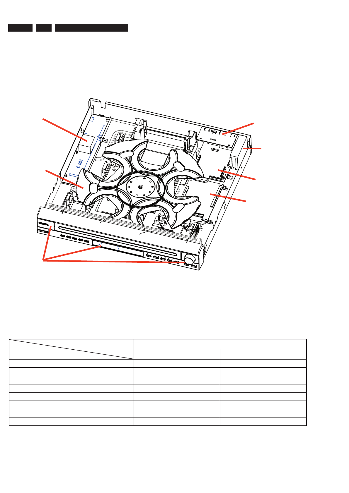
Dismantling Instructions & Service Positions
2.1 Dismantling of the SD5.5_5dis changer
1) The tray can be manually open by inserting a minus
screw drive and push the lever in the direction as shown
in Figure 1 to unlock the tray before sliding it out.
2) Slide out the tray and remove the Cover Tray (pos 110) as
shown in Figure 2.
Push lever in direction
shown to open the
tray manually
Figure 1
3) Loosen 7 screws to remove the Front Top.(pos 240)
- 2 screw each on the left & right side (pos 272)
- 3 screws A behind
2.2 Dismantling of the Tuner Module, AV Board,
SD6.3 ,Front Board, PSU Module
1) Loosen 2 screw B (see Figure 3a) to remove the Tuner
Module (pos 1040).
2) Loosen 4 screws C (see Figure 3b) to remove
AV Board 1.
3) Loosen 4 screws D (see Figure 3c) and 2 screws H (see
Figure 4a) to remove AV Board 2.
4) Loosen 2 screws E (see Figure 4a) to remove the PSU
Module.
5) Loosen 6 screws I (see Figure 4a) and 4 snap hooks to
remove Front Board.
- 1 snap hook each on the left & right side (pos 161).
- 2 snap hooks on the bottom side (pos 161).
B
A
Figure 3a
4) Loosen 6 screws G (see Figure 4a and 4b) to remove the
SD5.5_5dis changer.
Figure 2
C
Figure 3b
D
Figure 3c
Page 9
Catch
EN 9
Dismantling Instructions & Service Positions
HTS5500C/37/55
2.
H
E
F
2.3 Service Positions
Insert Thick
Insulation Sheet
in between the AV
Board 1 and 2.
G
I
Figure 4a
AV Board 2
Figure 5
AV Board 1
AV Board 1
G
Figure 4b
Thick Insulation Sheet
Thick Insulation Sheet
PSU
Figure 6
Thick Insulation Sheet
Front Board
Figure 7
Thick Insulation Sheet
SD6.3
Figure 8
AV Board 2
Page 10
EN 10
3.
HTS5500C/37/55
3. Diagnostic Software
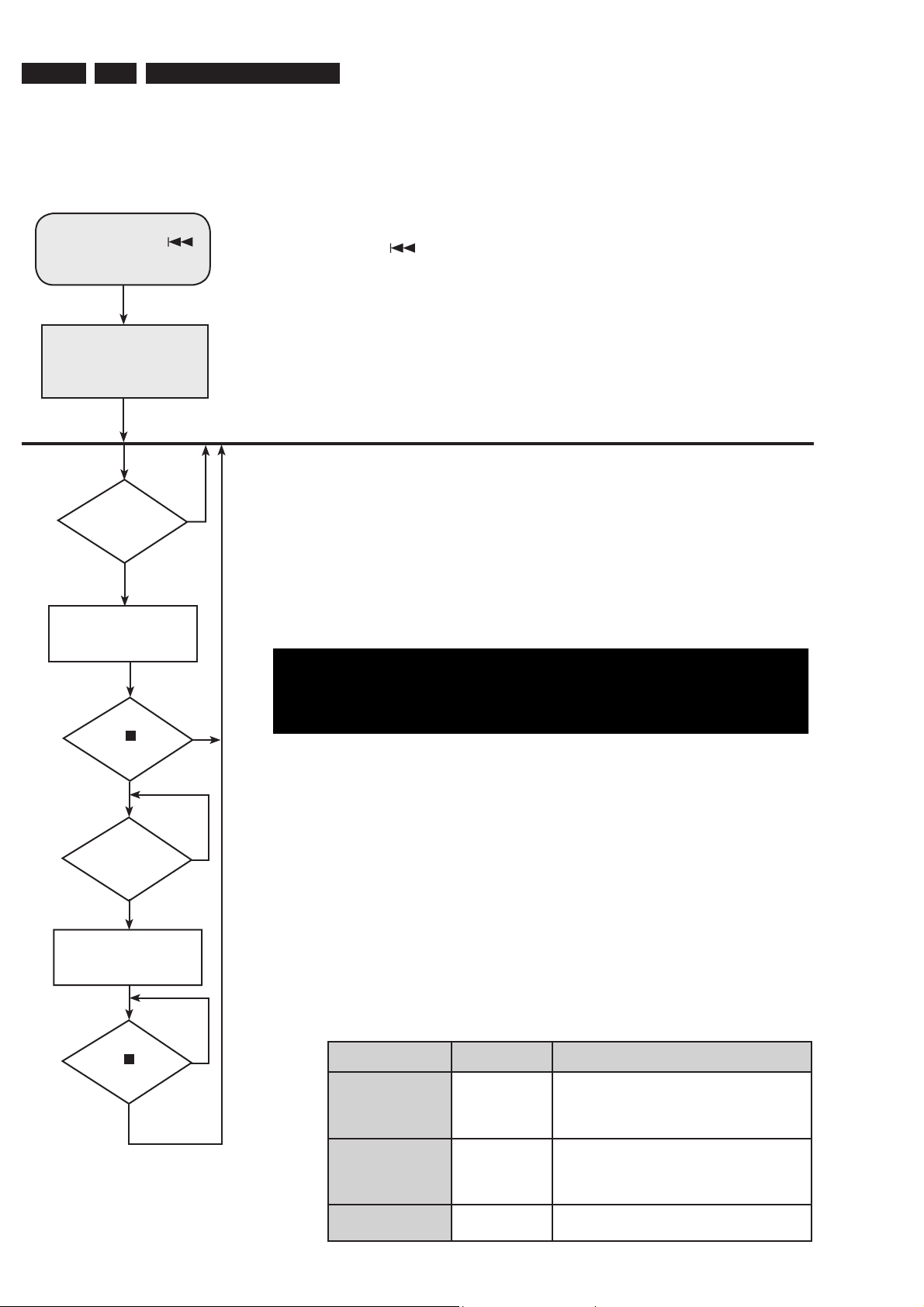
Service test program
To start service test program
hold open/close and
buttons depressed while
plugging in the mains cord
Hold open/close and buttons depressed till the Display shown “S-Vxx-yy”
Diagnostic Software
Display shows
“SERVICE”
followed by ROM version
“S-Vxx-yy”
Main Menu
Display Test
Key
“Display Test”
triggered?
Activate and display
“Pattern1”
“ ”
triggered?
n
“Display Test”
triggered?
Key
Key
S refers to Service Mode
V refers to Version
xx refers to Software version number of BEA
(counting up from 01 to 99)
yy refers to Software version number of Front uP
(counting up from 01 to 99)
Display Test
n
y
y
n
y
Following display patterns are used to test the display and its
connections to μP.
Pattern 1:
All display control pins are ON
All LEDs are ON.
- to check for open-circuits
Pattern 2:
Alternate display control pins are ON (Test Pattern: 0x55)
The following LEDs are ON:
DiscAvailable1
DiscAvailable3
DiscAvailable5
DiscActive2
DiscActive4
- to check for short-circuits
Activate and display
“Pattern2”
Key
“ ”
triggered?
y
(tbd)
n
TEST Activated with ACTION
EEPROM FORMAT
TEST
ROTARY
ENCODER TEST
LEAVE SERVICE
TEST PROGRAM
DISC 1 Load default data. Display shows “NEW”.
Volume
Knob
Disconnect
mains cord
Caution!
All presets from the customer will be
lost!!
Display shows value for 2 seconds.
Volume values increases or decreases in
steps of 1 until 0 (VOL MIN) or 40 (VOL
MAX) is reached.
Page 11

Diagnostic Software
HTS5500C/37/55
3.
EN 11
Reprogramming of DVD version Matrix
After repair, the customer setting and region code may be lost.
Reprogramming will put the set back in the state in which it has left
the factory, ie. with the default setting and the allowed region code.
HTS5x00 Software Version Matrix
Model
HTS5500
1
C/37
HTS5500
2
C/55
To reprogram do as follows:
1) Power up the set and select DISC source.
2) Open tray by press “OPEN/CLOSE” button on the set or press
and hold “STOP” button on the RC.
3) Press the following buttons on the Remote Control:
<9> <9> <9> <9> <AUDIO> <1> ......... for HTS5500C/37
<9> <9> <9> <9> <AUDIO> <2> ......... for HTS5500C/55
4) The display shows ‘YYYY-ZZ’ and the tray will close.
YYYY = model number (eg. 8300, 8500, etc.)
ZZ = slash stroke version (eg. 01, 69, etc.)
Key
Sequence
Open
Tray 9999
Audio 1
Open
Tray 9999
Audio 2
Region
LATAM 4 PAL yes
Region
Code
US 1 NTSC yes
TV
Type
PSCAN
Procedure for check Software version
1) Power up the set and select DISC source.
2) Open tray by press “OPEN/CLOSE” button on the set or press
and hold “STOP” button on the RC.
3) Press “DISPLAY” button on the Remote control.
4) The TV screen will shows:
SD6.3 Vxx YYYY-ZZ A BB
SERVO: nnnnnnnn REG:A
xx = version number
YYYY = model number (eg. 8300, 8500, etc.)
ZZ = slash stroke version (eg. 01, 69, etc.)
A = region code
BB = Front uP software version number
nnnnnnnn = servo version number
Trade Mode
Trade mode is a feature that will block all set keys when enabled.
It is for dealers to prevent customers from removing disc, changing
source etc using the set keys. Rotary and Remote Control (RC) keys
are still allowed inTrade mode.
To activate Trade Mode:
1) Power up the set and select DISC source.
2) Open tray by press “OPEN/CLOSE” button on the set
or press and hold “STOP” button on the RC.
3) Then press buttons <2> <5> <9> on the RC.
4) The display shows ‘TRA ON’ and the tray will close.
Trade Mode is now enabled.
To deactivate Trade Mode:
1) Power up the set and select DISC source.
2) Open tray by press and hold “STOP” button on the RC.
3) Then press buttons <2> <5> <9> on the RC.
4) The display shows ‘TRA OFF’ and the tray will close.
Trade Mode is now disabled.
Procedure to change Tuner Grid (not for all
versions)
In North and South America, the frequency step between adjacent
channels in the MW band is 10kHz (9kHz in some areas). The preset
frequency step in the factory is 9kHz.
IMPORTANT!
Changing the tuning grid will erase all previously stored preset
radio stations.
1) Press TUNER on the remote (or press SOURCE control on front
panel) to select “FM” or “MW”.
2) Press STANDY ON to switch the DVD system to standby mode.
3) While holding down SOURCE and PREV on the front panel,
disconnect and connect the power cord to the power supply
again.
-> The display will show “GRID 9” or “GRID 10”.
Helpful hints:
- GRID 9 and GRID 10 indicate that the tuning grid is in step of
9kHz and 10kHz respectively.
- The FM tuning grid also will be changed from 50kHz to 100kHz
or vice versa.
Procedure to upgrade software
1) Power up the set and select DISC source.
2) Open tray by press “OPEN/CLOSE” button on the set or press
and hold “STOP” button on the RC.
3) Place Upgrade CD-ROM with fi lename “HTS5500.bin” onto tray
and close.
4) The set will response and display the following:
- LOAD (After the disc is read, the tray will
open for you to remove the disc)
- ERASE (Erasing disc)
- WRITE (Writing disc)
- ERROR (if upgrade is unsuccessful)
- UPG END (if upgrade is successful)
- DISC->CLOSE->LOAD (Tray will close indicating that the
upgrade process is completed)
5) The whole process should not take more than 5 minutes.
Caution: Do not unplug the set until upgrade is completed.
Page 12

EN 12
Notes:
HTS5500C/37/553.
Diagnostic Software
Page 13
EN 13
HTS5500C/37/55
1
11
1
1
1
RDS_CLK
GND_D
PCM_Data_LR
GND_D
GND_D
GND_D
GND_D
PCM_Data_SLR
PCM_Data_Sub_Cen
GND_ND
1
1
GND_D
PCM_Data_LR
GND_D
RDS_CLK
RDS_DAT
SCL-DAC
SDA-DAC
GND_D
GND_D
GND_D
PCM_Data_SLR
PCM_Data_Sub_Cen
GND_ND
1
1
1
DNG
+1V8_Sense
GND_D
GND_D
+1V8
SCL-DAC
SDA-DAC
KLCSMCP
OL_ATADMCP
DNG
KLCMCP
KLCRLMCP
DNG
ted_ciM
DNG
tuo_FIDPS
DNG
05P
1
DNG
KLCSMCP
OL_ATADMCP
DNG
KLCMCP
KLCRLMCP
DNG
ted_ciM
DNG
tuo_FIDPS
DNG
05P
3eniL / 1TRACS
3eniL / 0TRACS
1
1
Y
C
V_DNG
SBVC
U_B
DNG
ETUM_VA
ni_ciM_ATAD_MCPFIDPS
V_DNG
1
1
+1V8_Sense
GND_D
GND_D
+1V8
2 eniL / CN
V_DNG
V_DNG
Y_G
V
_
D
N
G
V
_
R
V_DNG
1
1
1
1
1
V_DNG
1
1
1
RDS_DAT
3eniL / 1TRACS
3eniL / 0TRACS
2 eniL / CN
V_DNG
V_DNG
Y_G
V_DNG
V_R
V_DNG
Y
C
V_DNG
SBVC
U_B
DNG
ETUM_VA
ni_ciM_ATAD_MCPFIDPS
Block Diagram_HTS5500C_HYwk512
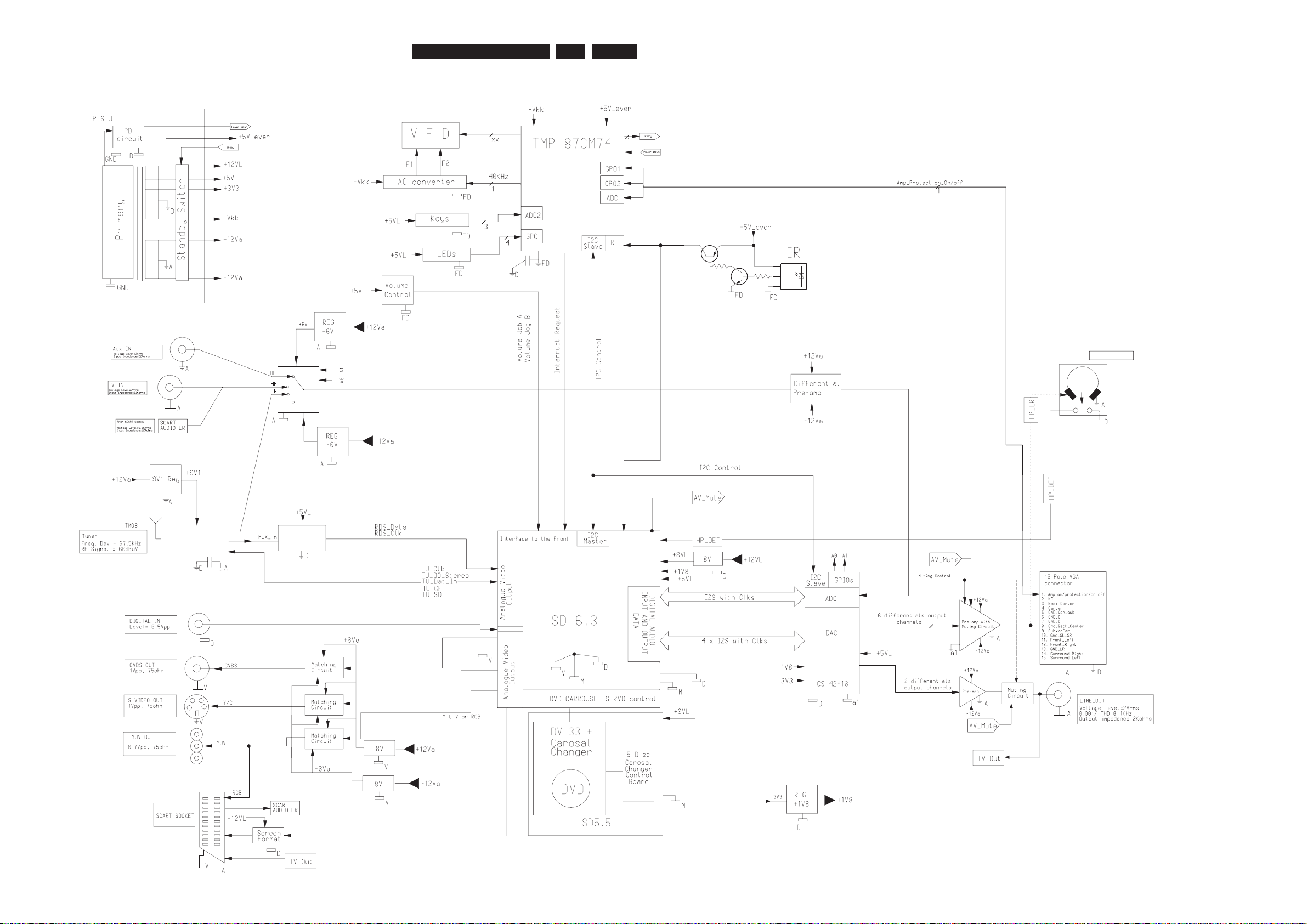
4. Set Block diagram
Set Block Diagram
4.
Page 14
EN 14
HTS5500C/37/55
5.
HEADPHONE
GND
OUT
VS
(SAA6581)
RDS
(TM 08)
TUNER
74HC4052
Wiring Diagram_3139 249 27191_HYwk511
5. Set wiring diagram
Set Wiring Diagram
Page 15
EN 15
HTS5500C/37/55
6. Panel Front Boards
Front Display - Component Layout
Panel Front Boards
6.
3139 243 3174 pt3 HY wk511
Front Display - Chip Layout
3139 243 3174 pt3 HY wk511
Page 16
EN 16
HTS5500C/37/55
Front Display - Circuit Diagram
Panel Front Boards
RESET
VASS
INT3
INT2
INT4
INT5
XTIN
XTOUT
SCL
V
P9<0:7>
V
SO1
5
6
7
6
5
4
3
2
29
28
27
26
25
24
2
3
4
TC1
SCK0
0
1
2
3
4
5
6
SI1
SCK1
DVO
TEST
VKKVDDVAREF
14
13
12
11
10
9
8
SDA
22
TC3
P1<0:7>
STOP
P2<0:2>
SI0
SO0
P3<0:2>
AIN
31
30
P5<0:3>
PD<0:4>
V3
P6<0:7>
V
P7<0:7>
V
P8<0:7>
23
16
21
20
19
18
17
P4<0:7>
AIN
1
0
15
VSS
PDO
2
1
XTAL
P0<0:7>
PPG
PWM
TC4
13
12
11
10
7
INT0
INT1
TC2
-30V
NC
1300 A5
1301 H3
1302 F3
1303 C4
1304 C5
23456789101112 13
12345678
*
*
*
E
F
G
H
I
A
B
C
D
E
F
G
H
I
1305 B1
1306 B1
2300 E4
2301 E3
2302 A3
2303 B4
2304 B5
2305 B4
2306 B4
DISC2_G
0V
1
NC
1F MORF/OT
-25V
-11V
2F MORF/OT
2307 B4
2308 I10
2309 I11
2310 I11
2311 I4
2312 E6
2313 E6
2314 E2
2315 C1
2316 C3
-25V
9101112 13
A
B
C
D
-32V
TO/FROM
NC
NC
NC
5V
-30V
-18V
DC vtg measured in STOP MODE
2317 C3
2318 C2
2319 B8
2320 D11
2321 D11
2322 E11
2323 F13
2324 F11
2325 C13
P S U
-18V
- NIL PHILIPS HTS5500
-30V
* 3342 - 150 YAMAHA C300
-25V
*
V
-32V
NC
-30V
A
2326 C13
2327 C13
2328 D13
2329 D13
2330 D13
2331 D13
2332 D13
-30V
5V2
2333 D13
2334 D13
2335 E13
2336 E13
2337 B7
2338 B7
2339 C5
2340 C6
2341 B7
3300 F4
3301 F4
3302 B3
3303 H10
3304 H11
3305 I11
5V
NC
NC
DISC3_G
5V
DISPLAY PANEL
5V3
-27V
3306 I12
3307 I11
3308 I11
3309 H4
3310 H4
3313 F6
3314 F6
3315 F6
3316 F6
3317 F6
3318 D6
3319 E6
3320 D6
3321 D3
3322 D3
Key_B02
-30V
5V
-25V
5V
#
-30V
+5VL
3323 C3
3324 C2
3325 C2
3326 D12
3327 E12
3328 E11
3329 F13
3330 F13
3331 F11
3332 D5
3333 B5
3334 B6
3335 B10
3336 B13
3337 B10
3338 B13
Optional
-22V
27V
-30V
0V
0V5
-20V
3340 H5
3341 H5
3342 H6
3343 H6
3344 E6
3345 G6
3346 I5
3347 I6
3348 I7
3349 I8
4301 H4
4302 H4
4303 E3
5300 B7
6300 A3
6301 A3
2V5
-25V
-27V
DISC5_G
DISC1_Y
1V6
DISC4_G
6302 I11
6303 C1
6304 H6
6305 I6
6306 H8
6307 I8
7300 B7
7301 B10
7302 F3
7303 E11
7304 E11
7305 E12
7306 H11
7307 D2
7308 C2
7309 I5
7310 H6
*
B
DISC5_Y
5V
5V
5V
7311 I7
7312 H8
T300 E4
T301 F3
T302 C10
T303 C13
T304 G4
T305 C11
T306 C12
T307 C12
T309 A5
T310 A5
T311 B3
T314 F6
T315 F6
T316 F6
FTD DISPLAY
OPTIONAL
NC
5V
5V
0V
T317 C6
T318 C6
T319 C6
T320 D6
T321 D6
T322 C6
T323 C6
T324 C6
T325 D6
T326 D6
T327 D6
T328 E6
NC
DISC3_Y
-30V
V23-
5V
-25V
T329 E6
T330 F6
T331 F6
T332 H3
T333 H3
T334 H3
T335 C3
T336 D2
T337 C11
-32V
GND_B
*
5V
NC
TO/FROM
*
DISC4_Y
T343 C11
T344 C11
T345 C11
T346 C11
T347 C11
T348 C11
T349 C4
T350 C4
T351 C4
T352 D4
T353 D4
T354 D4
T355 E12
T356 B10
T357 B13
T358 A5
T359 A5
T360 C2
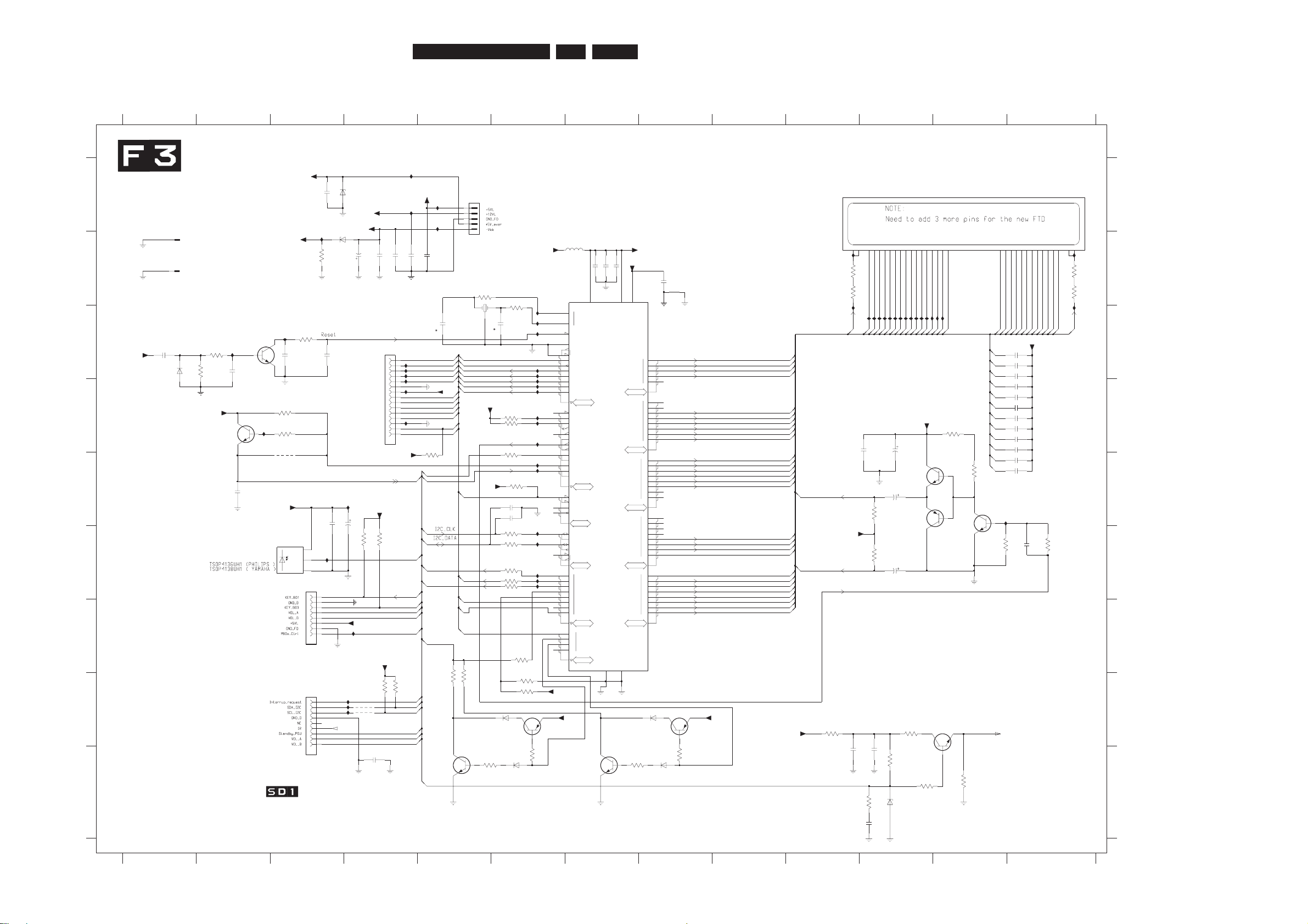
MONO BOARD SD6.3
2V
5V
NC
DISC2_Y
-30V
-25V
-30V
GND_FD
*
5V
T338 C11
T339 C11
T340 C11
T341 C11
T342 C11
FOR OEM MODELS ONLY
NC
DISC1_G
8MHz
-24V
+12V
*
6032
n001
6
7
8
9
1011
T320
09FMN-SMT-A-TF
1
2
3
4
5
87
7
9
8
GND_FD
1301
73
74
75
76
77
10
13
93
83 04
62
63
64
65
66
67
68
69
70
71
72
52
53
54
55
56
57
58
59
60
61
41
42
43
44
45
46
47
48
49
50
51
28
29
30
31
32
33
34
35
36
37
21
22
14
12
11
23
24
25
26
27
2
3
4
5
6
15
16
17
18
19
20
79
80
1
7333
7R4
Φ
MICROPROCESSOR
TMP87PM74ZF
7300
+5V_ever
3536 37 383940 41 4445567
89
GND_FD
1213 14 1516 17 18192
20 30
3132 33 34
1
FTD 12-ST-50GNK
7301
11011
RT-01T-1.0B
1305
GND_FD
1n0
2311
8032
n001
K01
6033
5033
K01
3304
1K2
2
GND
1
OUT
3
VS
7u4
9032
7302
7R4
8333
100p2328
K01
0333
3332
GND_FD
2K7
T325
T326
+5V_ever
T303
2329 100p
+5V_ever
1333
R074
17
0n1
7132
15
2
3
4
5
6
7
8
9
16
15FMN-SMT-A-TF
1303
1
10
11
12
13
14
603T
T357
22p2313
1K03314
p74
3032
3K3
T300
0133
2n2
0132
2K2
GND_FD
0433
GND_FD
GND_FD
3318 4K7
3307
47K
T356
3315 1K0
7032
p74
+5V_ever
+5VL
4302
+5V_ever
GND_D
T314
T311
10K
3324
GND_B
1K0
3323
GND_FD
GND_FD
GND_FD
4132
p22
4301
n33
6132
5300
2u2
743T
T304
503T
GND_FD
BC847BW
7308
4K7
3322
BC847BW
7307
T322
B-6.5ZDP
2036
1300
S5B-EH
1
2
3
4
5
p74
4032
n33
1232
T360
3317
5233
10R
100p
K01
1306
RT-01T-1.0B
1
2327
GND_FD
3320 4K7
543T
6333
2R2
7304
BC327-25
7303
BC337-25
3326
T316
T335
330R
3319 1K0
T323
n74
GND_FD
GND_FD
GND_VFD
9132
VFIL_DC
9033
3K3
0K1
8033
733T
833T
843T
VKK
T349
643T
T321
+5VL
T330
T350
T329
T358
+5V_ever
T309
T353
2K11433
+12VL
T302
T355
22u
2322
3232
p22
+5VL
+5V_ever
GND_FD
GND_VFD
5333
2R2
10R
3333
GND_VFD
T319
8332n33
T336
4303
T315
2324
22u
7233
R033
7u4
7332
8132
0n1
3342
T351
150R
2331 100p
+5V_ever
GND_FD
T310
9233
7K4
2312 22p
T331
2335 100p
+5V_ever
2325 100p
T318
100p2332
T317
+5V_ref
GND_B
T328
10R
3334
7312
BC857BW
BAS316
6306
6307
BAS316
10K
3348
K01
9433
GND_FD
+5V_ever
BC857BW
7310
7309
BC847BW
3346
10K
BAS316
BAS316
6305
6304
7433
K01
0432
p22
9332
p22
T334
3345
10K
GND_FD
1032
n001
2315
2u2
GND_FD
GND_FD
+12VL
BC847BW
7311
BC847BW
7305
T352
100p2326
T301
100p2334
+5V_ever
2333 100p
443T
100p2330
7K2
1033
0033
7K2
703T
5032
u22
6301
PDZ8.2-B
VKK
VFIL_DC
+5V_ref
2K73343
T324
T327
1432
7u4
u22
T332
GND_FD
GND_FD
0232
3036
613SAB
8233
R074
1304
0036
6V5C-483XZB
GND_FD
p74
2032
7306
BC847BW
T359
K01
2033
3303
100R
VKK
T333
100p2336
3313 1K0
4K7
3321
3316 10R
0032
GND_FD
GND_FD
u001
T354
GND_B
243T
343T
143T
933T
043T
GND_FD
5
6
7
8
910
1302
08FMN-SMT-A-TF
1
2
3
4
+5V_ref
10K
3344
DISC3_G
B01
B03
VOL_A
VOL_B
PBox_Ctrl
DISC5_G
DISC4_G
PBox_Ctrl
P14
P15
P16
DISC3_Y
DISC4_Y
DISC5_Y
B02
DISC2_G
DISC3_G
DISC4_G
DISC5_G
+5VL
DISC1_Y
DISC2_Y
STANDBY_LED
G4
G3
G2
G5
G12
G11
G10
G9
G8
G7
G6
G5
G4
G3
G2
G1
P1
P2
P3
P4
P5
P6
P7
P8
P9
P10
P11
P12
P13
FIL2
FIL1
G1
21G
61P
G8
G9
G10
G11
G12
2G1G3G4G5G
6G
G6
DISC1_G
INTRQ
DISC1_G
B01
SDA
STDBY_CTRL
1LIF
2LIF
8G
SCL
51P
IR
ioRC6
DISC2_G
DISC1_Y
DISC2_Y
DISC3_Y
DISC4_Y
DISC5_Y
FIL_DIR
IR
STANDBY_LED
IR
ioRC6
STDBY_CTRL
INTRQ
SDA
4P5P6P7P8P
9P
01P
11P
21P
31P
41P
VOL_B
VOL_A
SCL
G7
3P
B03
B02
11G
01G
9G
7G
1P
2P
3139_243_31714_31392433174 pt3 HY wk511
6.
Page 17
EN 17
HTS5500C/37/55
Key & Open/Close Board - Component Layout
Panel Front Boards
3139 243 3168 pt3 HY wk511
Key & Open/Close Board - Chip Layout
3139 243 3168 pt3 HY wk511
6.
Page 18

EN 18
HTS5500C/37/55
Key & Open/Close Board - Circuit Diagram
Panel Front Boards
3102 B6
3103 B7
3104 C4
4100 B3
4101 C3
4102 A5
4103 A5
4104 E6
4478 A6
1109 C4
1110 D5
1111 C8
1112 D5
I101 B2
I102 B2
I103 B2
I104 B2
I105 B2
I106 C2
I107 C2
ecruoS
POTS
ESOLC|NEPO
8
5100 B3
5101 C3
5102 E6
6100 B4
6101 B3
6102 C4
6103 D3
I100 B2
Key & OPEN|CLOSE
567
1113 C4
1114 B7
1115 E7
2100 B4
2101 C4
2478 A6
3100 B4
3101 B5
VERP
A
B
C
D
E
A
B
C
*
*
*
*
D
E
1100 B1
8
1234567
GHCX_CSID
3F MORF/OT
*
*
1102 A6
1103 E7
1104 B4
1105 B5
1106 B5
1107 B6
1108 B7
1234
TXEN
esuap/YALP
1
A3B
2
C
4
5
1101 E3
EVE
1102
8011
GND_B
9011
4102
3104
1115
RT-01T-1.0B
1
390R
0111
5101
2u2
150R
9
GND_HP
3100
1101
1
2
3
4
5
6
7
8
07FMN-SMT-A-TF
10K
2478
15u
5100
I106
I107
I105
I100
270R
3102
GND_B
4011
5011
8V6C-483XZB
0016
GND_FD
4101
GND_B
4100
3016
8V6C-483XZB
2016
8V6C-483XZB
2u2
2015
GND_B
4014
4478
GND_FD
3111
10K
4111
1
1111
RT-01T-1.0B
3103
390R
0012
p001
2
3
451103
TC38-103-01
6
7
1
910
I101
1
2
3
4
5
6
7
8
1
1100
08FMN-SMT-A-TF
1112
RT-01T-1.0B
220R
3101
I103
I104
I102
6011
7011
p001
1012
4103
8V6C-483XZB
1016
B01
B03
+5VL
B03
+5VL
VOL_A
VOL_B
VOL_A
VOL_B
B01
3139 243 31714_3139 243_3168 pt3 HY wk511
6.
Page 19

EN 19
HTS5500C/37/55
Panel Front Boards
Front key board - Component Layout
3139 243 3173 pt3 HY wk511
Front key board - Chip Layout
3139 243 3173 pt3 HY wk511
6.
Page 20

EN 20
HTS5500C/37/55
Front key board - Circuit Diagram
Panel Front Boards
34 78
5V
5V
3V8
78
C
D
E
F
A
B
C
D
E
F
1200 B1
1201 A4
1202 A5
1203 A5
1204 A6
1205 A6
1CSID
5CSID
3CSID
12
3209 D8
3210 D8
56
3213 E6
3214 E8
DISC2_PLAY
3V8
4CSID
DISC3_PLAY
2CSID
KEYS AND LEDs
123456
6204 C7
6205 C7
A
B
6208 D7
6209 E7
1206 A7
1207 B8
1208 A4
1209 B1
2200 A3
3200 A4
3201 A5
3202 A6
3203 A6
3204 A7
3205 B8
3206 C8
3207 C8
3208 C8
I208 C2
I209 C2
3211 D6
3212 D8
I212 C2
I213 C2
DISC4_PLAY
3215 E6
3216 F8
3217 F6
3218 F8
3219 F6
3220 B8
4200 A3
5200 A3
6200 A3
6201 B3
6202 B7
6203 C7
6206 C7
6207 D7
5V
DISC5_PLAY
YBDNATS
6210 E7
6211 F7
6212 B7
7200 D7
7201 D7
7202 E7
7203 F7
7204 F7
I200 B2
I201 B2
I202 B2
I203 B2
I204 B2
I205 B2
I206 B2
I207 C2
I210 C2
I211 C2
3V8
3F MORF/OT
5V
DISC1_PLAY
5V
3V8
I214 C2
3V8
5
6
7
8
9
1617
1
10
11
12
13
14
15
2
3
4
1200
15FMN-SMT-A-TF
15u
5200
3209
330R
6203
LTL-816YE
LTL-816YE
I206
I208
6205
3218
330R
7202
BC857BW
7203
BC857BW
1021
3220
330R
3207
330R
LTL-816YE
6206
6202
LTL-816YE
LTL-816YE
6207
LTL-816GE
6204
3216
330R
7204
BC857BW
6211
LTL-816GE
GND_B
I207
330R
GND_B
3205
0022
p001
3219
10K
330R
3206
3201
220R
6209
LTL-816GE
6208
10K
3213
LTL-816GE
10K
3211
7200
BC857BW
BC857BW
7201
3203
390R270R
I209
3202
I210
3208
330R
1026
8V6C-483XZB
0026
8V6C-483XZB
3021
5021
4021
3210
330R
LTL-816GE
6212
3214
330R
330R
3212
10K
3217
3215
10K
6021
3204
560R
2021
6210
I204
LTL-816GE
I203
I202
I201
I205
GND
I212
I200
I214
I213
4200
I211
8021
1
3200
150R
17
RT-01T-1.0B
1207
13
14
15
2
3
4
5
6
7
8
9
16
15FMN-SMT-A-TF
1
10
11
12
DISC1_G
DISC1_Y
DISC4_G
DISC3_G
1209
DISC5_Y
DISC2_G
DISC5_G
BO2
+5VL
DISC2_Y
DISC3_Y
DISC4_Y
DISC5_Y
STANDBY_LED
+5VL
STANDBY_LED
DISC1_G
DISC2_G
DISC3_G
DISC4_G
DISC5_G
BO2
DISC1_Y
DISC2_Y
DISC3_Y
DISC4_Y
3139 243 31714_3139 243 3173 pt3 HY wk511
6.
Page 21

EN 21
HTS5500C/37/55
Panel Front Boards
Video Connector Board - Circuit Diagram
Pr
S.VIDEO
6406 E7
6407 F7
6408 F7
7400 A6
7401 B6
7402 C6
7403 D6
7404 E6
7405 F6
T405 D8
T406 E6
T407 E7
T408 E8
T409 F6
T410 F7
T411 F8
3445 F5
3446 F5
3447 F5
4400 A6
4402 A7
4403 B6
4405 B7
4414 F6
4416 F7
5400 D2
5401 D2
6400 B7
6401 C7
6402 C7
6403 E7
6404 F7
6405 F7
3433 E6
3434 E5
3435 E7
3437 E5
T400 A8
T401 B8
T402 C8
T403 D7
T404 D6
1051 draoB VA oT
VIDEO CONNECTOR BOARD
3410 B6
3411 B7
3412 B5
3416 C5
3417 C4
3418 C6
3419 C7
3420 C5
3425 D6
4406 C6
4408 D6
4410 D7
4411 E6
4413 E7
Y
56789
A
B
C
D
3438 E5
3439 F5
3441 F6
3442 F5
3443 F7
2414 D3
2415 D7
2416 E8
2418 E7
2419 F8
2421 F7
2422 F8
3400 A5
3401 A4
3402 A6
3403 A7
3404 A5
3408 B5
3409 B4
1403 F8
2400 A8
2401 A5
2402 A7
2403 B8
2404 B5
2405 B7
2406 C5
2407 C7
3426 D5
3427 D7
3429 D5
3430 E5
3431 E5
123456789
1234
2413 D2
E
F
A
B
C
Coaxial In
CVBS
Pb
D
E
F
1400 C1
1401 A9
1402-A C9
1402-B B8
T401
2408 C8
2409 C8
2411 D2
2412 D2
2046
51C-483XZB
1
2
3
4
5
6
VGND
VGND
1403
LPR6520-P910F
3403
3419
DGND
4405
-8Va
VGND1
0046
51C-483XZB
51C-483XZB
5046
p022
8042
VGND
5400
2K2
5401
+5VVID
3439
1K5
3442
BC847B
7405
4414
VGND
4411
2404
10u 16V
V61
u001
3142
8046
51C-483XZB
VGND1
VGND1
7046
51C-483XZB
VGND1
+5VVID
+5VVID
VGND1
T400
9043
R57
4406
4400
6.3V
2418
470u
VGND
VGND
7401
BC847B
1K53426
100R
3441
+5VVID
+5VVID
4416
T404
VGND1
VGND2
VGND2
VGND2
0042
p022
K51
4043
9042
p022
+5VVID
+5VVID
+5VVID
3446 1K5
VGND
1046
51C-483XZB
75R3402
V61u001
1142
7400
BC847B
2407
470n
-8Va
R57
7143
3430
1K5
-8Va
3429 1K5
VGND
p022
3042
4402
6.3V
2402
470u
B-2041
G1031-0015PAL
87
1
4
2
3
5
6
VGND2
1402-A
LAP5100-1301G
K51
VGND
2143
3408
10K
VGND
7404
BC847B
VGND1
100R
3425
-8Va
VGND
2405
6.3V 470u
T409
T406
T407 T408
K51
0243
7403
BC847B
16V10u
2406
T405
-8Va
16V10u
2401
4142
n001
2142
n001
3437
1K5
51C-483XZB
4046
6046
51C-483XZB
-8Va
2242
p022
VGND1
4408
+5VVID
75R3410
3418
75R
BC847B
7402
VGND
5
6
7
8
9
10K
3400
14
15
16
17
18
19
2
20
3
4
20FMN-BTRK-A
1400
1
10
11
12
13
1
3
2
VGND2
YKC21-3416
1401
T402
T403
p022
6142
VGND2
R57
1043
3438
1K5
3411
2K23447
3435
68R
3427
68R
51C-483XZB
3046
VGND1
VGND2
4410
4413
6.3V
2415
470u
4403
VGND
1K5
3433
100R
VGND
3434
3445 1K5
DGND
9142
p022
2421
T411
6.3V 470u
T410
VGND2
3443
68R
10K
3416
3431
VGND
2K2
CVBS
SY
SC
Y_GREEN
Pb_BLUE
Pr_Red
Pb_BLUE
Pr_Red
0_2_5
DIG_IN
SY
SC
CVBS
Y_GREEN
0_2_5
DIG_IN
+5VVID
-8Va
3139 243 31714_3139 243_3172 pt3 HY wk512
6.
Page 22

EN 22
HTS5500C/37/55
Panel Front Boards
Video Connector Board - Component Layout
3139 243 3172 pt3 HY wk512
Video Connector Board - Chip Layout
3139 243 3172 pt3 HY wk512
6.
Page 23

EN 23
HTS5500C/37/55
AV Board
7. AV Board
AV Board - Top view layout
7.
Page 24

EN 24
HTS5500C/37/55
AV Board - Bottom view layout
AV Board
7.
Page 25

EN 25
HTS5500C/37/55
AV Board - Circuit Diagram (Part 1)
AV Board
11
1
T138 D12
T139 D12
T140 D11
T115 D3
T119 E3
T120 E3
T125 F3
T128 D2
T130 D12
T131 E11
T133 E12
T136 D11
T137 D12
T141 D12
T142 D12
T143 C12
7109 D7
7110 E7
7111 A9
T101 A7
T103 A7
T104 B7
T105 B7
T106 B7
T107 B7
T108 B7
T109 B7
T112 D3
T113 D3
T114 D3
T121 E3
T123 F3
T124 F3
3148 C11
3163 D4
3164 D4
3165 D4
3166 A9
3167 A9
4101 B11
7105-1 B10
7105-2 B11
7105-3 B10
3112 D7
3117 B9
3131 B11
3132 D4
3141 D6
3142 D7
3143 D7
3144 C12
3145 D6
3146 E7
3147 D8
2121 F4
2124 F4
2125 F4
2126 F5
AV_VIDEO
2130 F2
2131 B9
3110 B11
G
H
A
B
C
D
E
F
71112
A
B
C
D
E
F
3.6DS DRAOB ONOM
S.VIDEO
567 1112
123456
*
* OPTIONAL
3.6DS DRAOB ONOM
8910
G
H
1100 E12
1101 A6
1102 F2
2100 B11
1234
T124
8910
7
8
9
-8Va
16
17
18
19
2
20
3
4
5
6
1
10
11
12
13
14
15
+3V3
20FMN-BTRK-A
1100
T131
T142
3163
4
5
6
7
8
9
VGND2
1
10
11
12
13
14
15
16
2
3
7
8
9
1101
16FMN-BTRK-A
25
26
27
28
29
3
30
4
5
6
15
16
17
18
19
2
20
21
22
23
24
1102
1
10
11
12
13
14
30FMN-BTRK-A
DGND
DGND
3164
p74
5212
DGND
DGND
7
4212
p74
7105-1
TC7WHU04FU
1
84
7105-3
TC7WHU04FU
3
84
5
2100
100n
3131
DGND
T143
T139
2
T103
+3V3
7105-2
TC7WHU04FU
6
84
+5VL
+1V8
DGND
DGND
T121
T123
T136
T113
T112
T105
T115
T104
T114
DGND
T130
T128
2131
100n
330R
T133
3117
T106
VGND1
+5VVID
3165
T125
4101
DGND
+5VL
VGND
T140
T141
1212
p74
+5VL
+8VL
6212
p74
3132
T138
3147
10K
T108
1K0
3142
VGND2
T107
0312
n001
DGND
VGND
T119
T101
7111
BC847B
DGND
3167
K01
3166
4K7
+5VL
1413
K22
0K1
3413
1K0
3146
1M0
K22
5413
3110
2113
R019
4413
R57
3148
18K
T109
T137
BC847B
7110
7109
BC847B
T120
VGND1
Y
C
CVBS
G_Y
0|2|5
Standby_PSU
+3V3
AV_MUTE
PCM_Data_Mic_In
G_Y
C
DIG_IN_A
B_U
R_V
-8VA
KLCRL_MCP
KLCB_MCP
OL_ATADMCP
KLCMCP
+1V8_Sense
Standby_PSU
SCART1
0|2|5
SCART0
SCART1
SCART0
AV_MUTE
Y
CVBS
B_U
R_V
7.
Page 26

EN 26
HTS5500C/37/55
AV Board - Circuit Diagram (Part 2)
AV Board
COM
OUTIN
OSCO
RDSCL
SCOUT
VREF
RDDA
QUAL
VDDD VDDA
MPX
CIN
MODE
SYNC
TCON
OSCI
VSSAVSSD
T219 G2
T221 G2
T222 G9
T223 G2
5212 I6
5213 F8
5214 C13
6205 H12
6206 I12
6208 I13
6209 I12
6210 G3
7200 C8
7201 F13
7203 G12
T210 F2
T211 F2
T212 F2
T213 F2
T214 F2
T215 G2
T217 G2
T203 D2
T204 E2
T205 E2
T206 E2
T207 E2
T208 F2
T209 F2
3263 I5
3264 I13
3265 I9
3269 I10
3270 I10
3271 I10
3272 I10
3273 H9
3274 I9
3275 F1
3276 G2
T224 H2
T225 H2
T226 I9
T227 H3
4202 A12
5206 A10
5207 B10
5208 C2
5209 C4
5210 C13
5211 F8
3238 E6
3239 F5
3240 F6
3244 G7
3246 G10
3247 H10
3248 H12
3249 G4
3250 H7
3251 H9
3255 H10
7204 G6
7205 I13
T201 D2
T202 D2
3261 I6
3262 I10
3226 D4
3227 D5
3228 D5
3229 D5
3230 D12
3231 D12
3232 D6
3233 E5
3277 G2
3278 G3
4200 A12
4201 A12
3211 B10
3212 B5
3213 B10
3214 C5
3215 C10
3216 C5
3217 C10
3218 C3
3219 C3
3220 C10
3221 C10
3256 H4
3257 H10
3259 H4
3260 H5
2243 I6
3200 A6
3201 A5
3202 A5
3203 A7
3204 A5
3205 A6
3206 B7
3234 E5
3235 E5
3236 E5
3237 E6
2227 G5
2228 H5
2229 G7
2230 G7
2232 H13
2233 H7
2234 H7
2235 H12
2236 H4
2237 H4
2238 H9
3222 C6
3223 C10
3224 C6
3225 D6
2215 E3
2216 E4
2217 E4
2218 E8
2219 E4
2221 F6
2222 F7
3207 B7
3208 B6
3209 B5
3210 B6
2203 B10
2204 C2
2205 C3
2206 C6
2207 D6
2208 D11
2209 D12
2210 D12
2239 I9
2240 I12
2241 I12
2242 I6
A
B
C
D
E
F
G
H
I
A
2223 F7
2224 F7
2225 F1
2226 G14
123456
2211 D11
2212 D4
2213 D4
2214 D4
4 5 6 7 8 9 10 11 12 13
F
G
H
B
C
D
E
7 8 9 1011121314
123
9022
I
1200 B10
1201 E1
2200 A10
2201 A10
2202 B12
+3V3_AD
n001
+12Va
DGND
4200
4201
100n
2202
4323
K001
GND_A_REF
DGND
DGND
7203
BC547B
T206
1K0 3249
100R
3244
3272
-12Va_LO
22K
3215
1K0
3213
1K0
3211
1K0
5206
5209
DGND
+3V3_AD
2K2
8123
n001
8122
DGND
3222
V01u001
+5VL
4222
n001
DGND
LO_Left_+
+3V3_AD
K001
8223
GND_A_REF
GND_A
+5VL
GND_A_REF
AD1_CDIN
9
DGND
n001
1022
VLC
6
KCRL_CDA06KLCS_CDA
16
4NIDS_CAD
26
3NIDS_CAD
36
2NIDS_CAD
46
SCL_CCLK
7
SDA_CDOUT
8
2_DNGD
25
SLV
35
3_CN
45
55
KCMR
65
TUODS_CDA
75
2NICDA851NICDA
95
KCMO
45
GPO3
46
GPO2
47
GPO1
48
94
1_CN
DGND_1
5
05
2_CN
2_DV
15
38
LPFLT
39
4
VD_1
AGND_2
40
VA_2
41
GPO7
42
GPO6
43
44
GPO5
GPO4
-2BTUOA
13
+2BTUOA23+2ATUOA
AOUTA2-
33
AOUTB1-
34
AOUTB1+
35
36
AOUTA1+
AOUTA1-
37
MUTEC
1_AV
42
1_DNGA
52
62
-3BTUOA
72
+3BTUOA
82
+3ATUOA
-3ATUOA
92
DAC_LRCK
3
03
QV
71
+TLIF
81
DNGFER
91
DAC_SCLK
2
-4BTUOA
02
12
+4BTUOA
+4ATUOA
22
-4ATUOA
32
1
AD0_CS_
10
INT
11
RST_
12
AINR-
13
AINR+
14
AINL+
15
AINL-
16
DNGD
CS42418
7200
DAC_SDIN1
33R
3207
3206
33R
8322
GND_A_REF
2229
p74
560p
DGND
4322
n001
7222
DGND
7322
p001
GND_A
DGND
2228
2u2
33R
1K0 3256
3200
3261
220K
3623
2K2
33R
3205
4K73277
4K73276
DGND
4K7
3275
10u
2212
50V
3022
0u1
DGND
0022
0u1
0122
u74
0623
K74
DGND
1u0
2214
1u0
2216
33R
3201
n001
100n
2206
DGND
GND_A_REF
0021
3251
DGND
9523
K74
22R
3223
1K0
DGND
3422
p28
5212
LA-8481
12
DGND
DNGD
4M332
5207
T226
DGND
10K
3225
K001
7323
p086
1122
2207
1u0
+5VA
3232
10K
K001
9223
DGND
+5VA +5VA
MC78FC33H
7201
1
23
DGND
DGND
GND_A_REF
2215
470n
T222
1K0
1K0
3221
p001
3217
n001
6322
5210
5022
1125
+5VL
V01u001
5322
+5VA
+5VA
3274
22R
GND_A_REF
3273
22R
K001
7223
p74
2422
2219
50V
+5VA
LO_Left_-
10u
22R
3262
22R
3257
DGND
22R
3247
V01u001
6222
GND_A_REF
+3V3_AD
22R
3255
22R
3265
DGND
T204
DGNDDGND
DGND
5323
+5VL
+5VL
+5VL
K001
K001
6223
1422
GND_A_REF
Mutec
4623
5K1
BC547B
7205
BAS316
6209
3323
6206
BAS316
8323
K001
K001
K001
6323
9322
T217
u001
T219
-12Va
T221
3220
1K0
T201
T203
T202
GND_A_REF
3204
T205
DGND GND_A_REF
33R
+5VL
5214
0422
K01
0523
2230
1n0
K001
0423
K001
9323
33R
3222
2n2
2208
22R
3270
-12V_Mute
+12Va_Dif_LFE
-12Va_Dif_SLR
+12Va_Dif_SLR
-12Va_Dif_LFE
22R
3269
4202
3202
33R
5208
T207
3209
33R
3216
33R
15
5
21
3
6
11
7
9
4
1314
1
2
16
810
7
8
9
7204
SAA6581T
Φ
24
25
26
27
28
29
3
30
4
5
6
15
16
17
18
19
2
20
21
22
23
1
10
11
12
13
14
30FMN-BTRK-A
1201
DGND
LO_Right_+
LO_Right_-
3125
6V5C-483XZB
5026
p074
3122
p074
7122
+12Va_LO
3224
33R
3246
22R
T225
T223
5222
p001
DGND
4022
0u1
33R3203
DNGD
1323
T215
K01
+3V3M
BAS316
6210
T224
DGND
GND_A
0323
K01
DGND
T209
T208
T210
T212
DGND
DGND
T213
GND_A_REF
T214
8026
9V3C-483XZB
GND_A_REF
GND_A
GND_A
9123
2K2
1222
TU_MTK
GND_A_REF
2222
V057u4
n001
+3V3_AD
2K1
8423
3271
22R
3214
33R
33R
3212
3210
33R
3208
33R
3278
33R
-12Va_Dif_LR
+12Va_Dif_LR
p065
DGND
T227
3322
T211
DGND
2322
0u1
+12VA
+5VL
AMP_ON
AV_MUTE
PWR_DN
DAC_RST
HP_Det
+3V3_A
DAC_LEF_-
MUTE_SL_SR
+3V3_AD
+3V3_A
+3V3_DAC
Source_sel_A0
Source_sel_A1
AMP_ON_LR_SUB_com
AMP_ON_SLR_com
MUTE_LR_SUB
MUTE_CEN
Tu_SD
TU_CE
TU_Dat_In
TU_DO_STEREO
DIG_IN_A
TU_CLK
PCM_Data_LR
PCM_Data_SLR
PCM_Data_Sub_Cen
PCM_Data_Mic_In
PCMCLK
+12VA
TU_RDS_IN
Right_In
Left_In
SDA_DAC
SCL_DAC
+5VA
PCM_Data_Sub_Cen
PCM_Data_SLR
PCM_Data_LR
SCL_DAC
DAC_L_-
SDA_DAC
DAC_LEF_+
DAC_C_+
DAC_C_-
DAC_RS_-
DAC_RS_+
DAC_LS_+
DAC_LS_-
DAC_R_-
DAC_R_+
DAC_L_+
PCM_LRCLK
PCMDATA_LO
PCM_BCLK
DAC_RST
7.
Page 27

EN 27
HTS5500C/37/55
AV Board - Circuit Diagram (Part 3)
AV Board
6312 C8
6313 F8
6314 F10
7101 G7
7300-1 A4
7300-2 B4
7301-1 E4
7301-2 D4
7302-1 H4
7302-2 G4
7310 A7
7311 A7
7312 A9
7313 A9
7314 B7
7315 D7
7316 E7
3394 G10
3395 G8
3396 H8
3397 G8
3398 H8
3399 H7
3400 H8
4300 H7
4301 E13
4302 E13
4303 C7
6300 C7
6301 C7
6302 C7
6303 C7
6304 F7
6305 D13
Front_Left
6306 F7
6307 F7
6308 F9
6309 F9
6310 F9
6311 F9
3368 D8
3369 D10
3370 D10
3371 D10
3372 D10
3373 D8
3374 D8
3375 D8
3376 D8
3377 E7
3378 E8
3379 E7
3380 F7
3381 E8
3382 C9
3384 E9
3385 F9
3386 E10
3389 G7
3390 G8
3391 G10
3392 G10
3393 G10
3345 I3
3346 I2
3347 I2
3348 I4
3349 I3
3350 A7
3351 A8
3352 A10
3353 A10
3354 A10
3355 A10
3356 A8
3357 A8
3358 A8
3359 A8
3360 B7
3361 B8
NC
3362 B7
3363 B7
3364 B8
3367 D7
3327 E3
3328 F3
3329 F2
3330 F4
3331 F3
3332 F3
3333 F2
3334 G3
3335 G3
3336 G3
3337 G2
3338 G4
3339 G3
3340 H3
3341 H2
3342 H2
3343 H3
Surround_Right
Surround_Left
AV_AUDIO ( Dif_Amp for 6-channels )
3344 H3
3310 C3
3311 C2
3312 C3
3313 C2
3314 C5
3315 C3
3316 D3
3317 D2
3318 D3
3319 D3
3320 D3
3321 D2
3322 E4
3323 E3
3324 E3
3325 E2
3326 E3
Center
PB_Ctrl
2339 D9
2340 E9
2341 F7
2342 F8
2343 F10
2344 F10
2345 G9
2346 H9
2347 E2
2348 G7
2349 H7
2350 D13
3300 A3
3301 A2
3302 A3
3303 A2
3304 A3
Gnd_Cen_sub
Gnd_SL_SR
3305 A2
3306 B5
3307 B3
3308 B3
3309 B2
2316 E4
2317 F4
2318 F3
2319 G4
2320 G2
2321 G4
2322 G3
2323 H5
2324 H5
2325 H4
2326 I4
2327 H2
2328 H2
2329 I3
2330 I2
2331 A6
2332 B6
2333 D6
2334 E6
2335 A9
2336 A9
2337 B8
2338 B8
9 1011121314
A
B
C
D
E
F
G
H
I
A
B
Subwoofer
GND
Gnd_D
NC
Front_Right
GND_LR
2314 D2
2315 E3
Gnd_D
1234567891011121314
12345678
C
D
E
F
G
H
I
1300 D14
2300 A5
2301 A5
2302 A5
2303 A3
2304 A2
2305 B3
2306 B3
2307 C5
2308 B2
2309 C3
2310 D5
2311 D4
2312 D5
2313 D4
7317 D9
7318 E9
7319 E7
7320 E9
7321 F7
7322 H7
7323 G9
7324 H9
T300 A11
T301 A11
T302 A11
T303 D11
T304 D11
T305 D11
T306 D14
T307 D12
T308 E12
2321
100p
3323
6K8
100p
2313
5K6
3320
150K
5
6
7
84
3362
GND_A
LM833D
7301-2
3377
680R
7300-1
NJM4556AM
3
2
1
8
4
2324
100n
1K5
6K8
3331
100R
3333
DGND
3352
T300
2K2
3326
3318
2K2
2K2
3338
51C-483XZB
5036
BAS316
6302
6301
BAS316
3325
1K5
2312
-12Va_Dif_LR
2n2
7432
100n
3393
2n2
0232
1K5
100R
3321
5K6
3316
8032
2n2
6K8
3311
3334
2K2
100K
GND_A
GND_A
3379
p0010532
BC847B
3322
2K2
7310
2K2
3314
3310
2K2
2K2
3306
2323
100n
T302
T303
GND_A
T301
p001
9332
1u0
GND_A
GND_A
2334
3328
1K5
3309
5K6
3317
1K5
4132
2n2
2317
GND_A
100p
7320
5
6
7
84
BC857B
7302-2
LM833D
7232
2n2
6307
BAS316
3368
680R
3373
1K0
1
84
7302-1
LM833D
3
2
4
GND_A
GND_A
GND_A
LM833D
7301-1
3
2
1
8
2349
10u 50V
2K2
3302
3374
1K0
2301
100n
+3V3M
2K7
3343
GND_A
GND_A
GND_A
+3V3M
5K6
3336
8232
3342
9132
p001
p033
680R
3351
+12Va_Dif_LFE
GND_A
K001
3633
3384
100K
680R
3390
7u4
GND_A
GND_A
4432
3364
47K
1K5
3313
6K8
7u4
3315
100R
3371
3432
100R
3369
100R
3354
3386
47K
T304
680R
3378
+12Va_Dif_LR
0432
GND_A
p001
22K
3344
7101
BC847B
680R
3367
GND_A
1u0
2333
GND_A
7316
BC847B
p001
GND_A
1K0
3356
6032
DGND
-12Va_Dif_SLR
GND_A
BAS316
6300
2331
-12Va_Dif_LR
DGND
1u0
1K0
3398
3
4
5
6
7
8
9
16 17
+12Va_Dif_SLR
1
10
11
12
13
14
15
2
1300
1216-004-15S-AAC
3361
680R
3359
1K0
7u4
1432
7u4
2432
2n2
2322
100R
3391
p001
6432
GND_A
5432
4300
p001
6311
BAS316
GND_A
5K6
3332
GND_A
GND_A
1833
K74
GND_A
1K0
3395
K74
3533
+12Va_Dif_SLR
-12Va_Dif_SLR
3400
680R
3399
680R
3324
5K6
K74
5533
BC857B
7314
6306
BAS316
7321
BAS316
7322
BC847B
T308
T307
1K0
3376
1K0
3375
680R
3389
GND_A
1u0
2348
7323
BC847B
7324
1K5
GND_A
BC847B
3341
680R
3350
p001
3032
2n2
2329
3347
22K
3349
2933
BC847B
K74
+12Va_Dif_LFE
GND_A
7315
3301
3346
1K5
1K5
2n2
4032
2318
2n2
3329
1K5
p001
6K8
3335
p001
6332
GND_A
5332
6K8
GND_A
GND_A
3339
6K8
3327
7u4
7332
100p
2307
GND_A
3312
5K6
2n2
2315
6310
BAS316
1K0
3396
GND_A
6309
BAS316
+3V3M
T305
7312
BC847B
3360
GND_A
2332
1u0
680R
+12Va_Dif_LR
3380
100K
BC847B
7311
3330
2K2
100n
2300
5
6
7
8
4
7300-2
NJM4556AM
6314
BAT54 COL
GND_A
DGND
GND_A
6132
p001
3319
6K8
p001
1132
7318
BC847B
7313
BC847B
3337
1K5
330p
2330
7317
BC847B
1K0
3357
GND_A
3348
2K7
-12Va_Dif_LFE
4302
4301
3397
DGND
3305
1K0
1K5
BAS316
6308
3385
100K
3308
5K6
2n2
2309
6304
BAS316
3034
0K1
2833
6312
BAT54 COL
BAT54 COL
6313
6K8
3303
7u4
K74
4933
8332
1K0
3358
5K6
3300
2n2
2305
p074
5232
3340
12K
-12Va_Dif_LFE
K74
0733
K74
2733
7319
BC857B
470p
2326
12K
3345
T306
GND_A
100n
2310
BAS316
6303
GND_A
3307
6K8
2302
100p
PBox_Ctrl
PWR_DN
PWR_DN
PWR_DN
3304
5K6
Mutec
HP_Mute
-12V_Mute
Sub_Mute
-12V_Mute
-12V_Mute
DAC_RS_-
DAC_LEF_-
Sub_Mute
HP_Mute
HP_Mute
MUTE_LR_SUB
MUTE_SL_SR
MUTE_CEN
AV_Mute
AV_Mute
AV_Mute
Mutec
Mutec
DAC_L_+
DAC_C_-
DAC_R_+
DAC_LS_+
DAC_RS_+
DAC_LEF_+
DAC_C_+
HP_R
HP_L
6CH_SR
6CH_SL
DAC_LS_-
DAC_R_-
DAC_L_-
7.
Page 28

EN 28
HTS5500C/37/55
AV Board - Circuit Diagram (Part 4)
AV Board
NCNC
A
REF
K
COM
OUTIN
COM
OUTIN
COM
OUTIN
COM
OUTIN
T403 C3
T404 C3
T405 C3
T406 C3
T407 C3
T411 D4
5404 C11
1402 B4
GND
SPMS MORF
+3V3
GND_D
+12Va
Gnd_a
D
E
F
G
H
I
A
7401 B6
7402 C6
7403 D10
7404 D7
7405 E4
7406 G5
7407 H6
3490 D7
B
C
D
E
F
G
H
I
1401 B3
T401 B3
T402 B3
3495 C4
4401 B4
4402 B4
4404 E3
4405 F2
4408 C10
4409 D7
4410 G11
4411 H11
5401 C5
5402 C6
5403 C8
2423 H9
5405 D11
Standby_PSU
IN
2428 H11
2609 C3
3480 D9
3481 D9
3482 G4
3483 G5
3484 I4
3485 I5
3486 C6
3487 C6
3488 D6
3489 D6
2409 D11
3491 D6
GND_D
3492 D7
3493 G5
3494 H5
2411 E3
2412 E3
2413 F3
2414 F4
2415 G5
2416 G6
2417 G9
2418 G9
2419 H9
2420 G9
2421 H9
2422 G9
B
2424 H6
+3V3
-12Va
2425 H6
2426 I5
2427 G11
2402 C7
2403 C11
2404 C11
2405 D5
2406 D6
2407 D10
2408 D11
1403 E3
2410 D10
+5VL
Power_Dn
AV_VIDEO (Supply Distribution )
123456789101112
A
C
L7908
GND_D
2
OUT
+8V_5CDC
1404 E4
1405 F2
2401 C7
+12VL
123456789101112
LD1117DT33
7403
1
3
IN
K
3
12
4
7401
BCP53
7404
TS431L
A
5
K51
8843
68R
3487
6042
n001
DGND
+1V8
u01
4402
5042
V05
2K8
2943
BC847B
7402
1
3
2
DGND
5242
n001
2422
100n
100n
100n
2423
2418
33u
5404
4409
+8VL
5405
33u
3495
100R
2410
100u
u001
3142
DGND
T401
4401
100n
GND_A
2
GND
1
IN
3
OUT
2417
L7808CD2T
7405
3494
+3V3
u001
-8Va
1R0
4242
-12Va
6242
u001
DGND
VGND
1403
T2A
DGND
4404
7406
L78M05CDT
2
13
4411
+5VL
GND
2
IN
1
OUT
3
VGND
7407
u001
6142
5142
u001
V52u74
8042
+12Va
T411
100n
2419
T407
+12VL
2142
n001
T403
T406
4410
3042
V52u74
GND_ME2
T402
1404
B2B-PH-K
1
2
GND_ME1
+3V3_POWER
DGND
4405
+3V3_POWER
2428
10n
T405
4408
T404
+3V3_DAC
2K2
1943
0943
K21
1042
V05u01
10n
2427
100n
2420
u001
1142
1402
3493
1R0
9062
n001
4142
u001
2042
5403
DGND
DGND
DGND
n001
7K2
3843
2843
7K2
7K2
4843
5843
7K2
1843
0843
0K1
0K1
5402
9843
2K8
9042
n001
VGND
VGND
2421
100n
n001
7042
GND_A
9
1405
10
11
12
2
3
4
5
6
7
8
1401
B12B-EH-A
1
22R
3486
DGND
+5VVID
DGND
4042
n001
DGND
DGND
PWR_DN
5401
+12Va
+5VL
+12VL
Standby_PSU
-12Va
-12VA
7.
Page 29

EN 29
HTS5500C/37/55
AV Board - Circuit Diagram (Part 5)
AV Board
G4
0
3
2
VDD
VEE VSS
1
0
3
2
1
4X
030
1
F
G
H
I
T515 F3
T516 F3
T517 F3
T518 G3
E
F
G
H
I
A
B
C
D
E
6789101112
1502 A1
1503 A2
1504-1 F2
1504-2 F2
1504-3 D2
1504-4 G2
2501 B6
67891011
12
AV_INPUT_CIRUCIT
345
2502 B7
2503 B11
2504 B3
2505 B4
13 14
12345
2524 G9
2525 G10
2526 G4
2527 G8
2528 H8
2529 H10
2530 H4
12 13 14
A
B
C
D
3504 B6
3505 B6
3506 B12
3507 B4
3508 C11
3509 D10
3512 D3
2508 D6
2509 D6
2510 D2
2511 D3
2512 D5
2513 D5
2514 E10
2516 E6
2518 E5
2519 E5
2520 F6
2521 F5
2522 F5
2523 G8
3520 E5
3521 E5
3522 E6
3523 F5
2531 H6
2532 H6
2533 I10
2534 I9
2535 I8
2536 I10
2537 G8
2538 H8
2539 H5
3501 A6
3502 A6
3503 B12
3540 H5
3542 H9
3543 H11
3544 H7
3545 I10
3546 I10
3547 I9
3513 C11
3514 D3
3515 C10
3516 D6
3517 D6
3518 D10
3519 E10
4501 C7
4504 E11
4505 E11
4506 E2
3524 F5
3525 F6
3526 G9
3527 G11
3528 G7
3529 G10
3530 G10
3531 G4
3532 G5
3533 H9
3534 H10
3535 H6
3536 H8
3537 H9
3538 H6
3539 H4
T504 A3
T505 A3
T506 A3
T507 A3
T508 B3
T509 B3
T510 B3
3548 I10
3549 I8
3550 I9
3551 G5
T511 D2
T512 D2
T513 D2
T514 F3
4507 B3
6501 B4
6502 H7
6503 H7
7501 B4
7504 G5
7505 G5
7506 H5
7507-1 G9
7507-2 H9
7508 B9
T501 A3
T502 A3
T501
3526
15K
GND_A
T502
4252
3530
p28
7u4
K01
1353
GND_sel
V3.6
2352
12K
4505
2520
3549
2516
1u0
1u0
3K3
3514
3512
3K3
6502
BAS316
p001
1052
4504
100R
3508
330R
3544
4501
7053
GND_A
GND_A
GND_A
R051
8
12
1
14
5
15
2
11
4
13
3
7508
HEF4052B
MDX
10
9
6
61
7
01C-483XZB
GND_TU
-12Va_LO
6501
T507
T509
LO_Right_+
12K
3536
3551
47K
10K
3534
1352
V3.67u4
3532
1K5
GND_sel
7504
BC847B
T514
T517
T518
T516
GND_sel
+12Va_LO
GND_sel
n001
9352
GND_sel
p001
0352
1K5
3540
p001
6252
3052
V610u1
K074
9053
2529
470p
3547
15K
GND_A
4506
3521
GND_TU
100n
2523
7054
2
3
4
5
6
7
8
9
1502
13FE-BT-VK-N
1
10
11
12
13
470p
2536
82p
2528
15K
3533
3524
-12Va_LO
GND_A
GND_sel
GND_sel
5153
GND_sel
3523
3K3
GND_sel GND_sel
K074
6503
3520
BAS316
LO_Left_-
3K3
2508
1u0 GND_sel
T512
GND_sel GND_sel
3543
10K
p074
3352
3546
p28
8K2
p001
2052
4352
GND_sel
T511
GND_sel
p001
T510
7153
K86
2152
GND_sel
p001
3152
TU_MTK
T505
15K
3542
T504
GROUND
YKC21-3427
1504-4
01
11
T506
1504-3
7
9
8
4
6
5
YKC21-3427
3
2
YKC21-3427
1504-2
YKC21-3427
1504-1
1
GND_A
GND_A
GND_A
GND_sel
GND_sel
GND_A
8K2
3537
p86
0152
GND_TU
100n
2504
p86p86
81521252
GND_A
7505
BC857B
K01
9353
1K0
3538
GND_A
GND_A
5
6
7
8
4
GND_A
LO_Left_+
7507-2
LM833D
T513
3518
10K
3548
3550
10K
2
1
84
82p
2535
7507-1
LM833D
3
3528
330R
K86
6153
K051
4053
560R
3501
560R
3502
GND_A
p001
7506
BC847B
9152
GND_A
100R
3513
K86
GND_sel
GND_sel
2253
22u 16V
22u 16V
2538
LO_Right_-
2537
GND_selGND_A
GND_sel GND_sel
GND_sel GND_sel
5253
K86
1u0
2509 GND_sel
p001
2252
0u1V61
4152
5052
V52u001
7501
BC368
5053
K051
T508
3527
10K
5252
p074
GND_sel GND_sel
GND_A_REF
12K
3529
10
11
2
3
4
5
6
7
8
9
1503
1
5K6
3503
8K6
9153
12K
3545
1152
p86
GND_sel
8K6
+3V3M
+12Va_LO
6053
100n
2527
GND_A
K74
5353
LINE_L
LINE_R
T515
TU_DO_STEREO
Tu_CLK
TU_Dat_In
TU_CE
TU_RDS_IN
Tu_SD
AV_Mute
Mutec
-12V_Mute
Left_In
Source_sel_A0
Source_sel_A1
Right_In
+12VA
-12Va
+12VA
7.
Page 30

EN 30
HTS5500C/37/55
AV Board
AV Board - Circuit Diagram (Part 6)
3606 B4
3607 C3
3608 C4
3609 C5
100u 10v
12
C
D
E
A
B
C
D
E
1601 C7
2601 B2
2602 B5
2603 C5
2604 C2
2605 D3
2606 D3
2607 D4
2608 D4
3601 B2
3602 B4
3603 B6
3604 B5
3605 B3
78
A
B
1XXX
1
4
5
3
2
T601 B7
T602 B7
T603 B7
T604 B7
TC38-103-01
FD
345678
123456
AV_HEADPHONE
100u 10v
3610 C2
3611 C4
3612 C6
3613 D2
3614 D5
3615 D5
3616 D3
3617 C4
3618 D5
6601 D2
6602 D2
6603 E2
6604 E3
7601 B3
7602 B4
7603 C3
7604 C4
7605 C3
7606 D5
GND_A
7
6
8062
0u1
0u1
7062
1K0
3615
4063
8K1
GND_A
8K1
9063
33R
3612
3603
T603
3611
150R
33R
3616
1K0
8163
7K4
2601
3602
150R
6603
BAS316
6602
BAS316
6601
BAS316
2604
+3V3M
BC857B
7605
150R
3610
5062
GND_A
7u4
7u4
27K
3613
6062
3601
150R
BC817-25
7603
BAT54 COL
6604
7601
BC817-25
GND_A
p001p001
20623062
1K0
3608
3606
1K0
GND_A
BC817-25
7602
3607
1K0
1K0
3605
3617
47K
89
1
2
3
4
5
6
7
07FMN-SMT-A-TF
1601
7604
BC817-25
T604
T602
T601
4163
K72
B748CB
6067
+3V3M
HP_Mute
PWR_DN
MUTE_LR_SUB
AV_Mute
Mutec
HP_R
HP_L
HP_Det
-12V_Mute
HP_Det
PBox_Ctrl
7.
Page 31

EN 31
HTS5500C/37/55
8. Powerbox Spk Assy SW5500C
Power Supply Unit - Top view layout
Powerbox Spk Assy SW5500C
8.
Page 32

EN 32
HTS5500C/37/55
Power Supply Unit - Circuit Diagram (Part 1)
1
1
2
2
3
3
4
4
5
5
6
6
7
7
8
8
D D
C C
B B
A A
Fp001
205C
Fp001
105C
Fp001
305C
Fp001
405C
7K4
525R
YALER
A
1
K
2
D515
Di ode 1N4148
YBTSV21+
1
2
3
6NOC
NIP3HE
105D
3004N1 edoiD
A1K
2
305D
3004N1 edoiD
205D
3004N1 edoiD
405D
3004N1 edoiD
R021
105R
2
1
V052HA8T
1F
21
V052HA8T
2F
W2/1 22.0
115R
W2/1 22.0
215R
2
1
3
4
025D
0101UBG
1 2
4 3
RL501
RELAY-2P
B
2
C1E
3
405Q
B745CB
505C
V36/FU0074
605C
V36/FU0074
015C
V52/FU0001
115C
V52/FU0001
V001/U1.0
705C
V001/U1.0
805C
V001/U1.0
215C
V001/U1.0
315C
2
3
4
6
7
8
9
01
11
21
1
C 031
V021
V01
V011
5
31
41
105RT
T1SNART 2-2SNART
k1
625R
1
2
9NC
A-HE-B20B
NI
1
TUO
3
2
MOC
1U
50L87
NI1TUO
3
2
MOC
2U
21L87
NI2TUO
3
1
MOC
3U
21L97
CD+
CD-
CD-
CD+
YBTSV21+
Fp001
415C
U1.0
615C
U1.0
815C
U1.0
515C
U1.0
715C
U1.0
915C
V21+
V21-V5+
1
2
3
4
5
6
7
8
9
01
11
21
31
41
51
19NOC
A-HE-B51B
V21+
V21-
025C
V52/FU01
125C
V52/FU01
225C
V52/FU01
V5+
1
2
3
4
5
6
7
8
9
01
11
21
31
41
51
59NOC
A-HE-B51B
V5+
V21+
CD+
1
2
3
4
5
6
7
8
7NC
A-HE-B80B
CCV+
CCV-
CCV+
CCV-
1
2
3
4
5
6NC
A-HV-B50B
1
2
3
4
5
6
7
8
2NC
A-HE-B80B
BCP REMROFSNART
1
2
3
1NOC
nip3hv
M01
09R
V572/Fu10.0
59C
1 2
101RV
)NOITPO(rotsirav
1
2
3
4
5
6
3NC
A-HE-B60B
V032/V021 CA
Powerbox Spk Assy SW5500C
8.
Page 33

EN 33
HTS5500C/37/55
Power Supply Unit - Circuit Diagram (Part 2)
1T
61EE
+-
Powerbox Spk Assy SW5500C
8.
Page 34

EN 34
HTS5500C/37/55
Interface - Top view layout
Powerbox Spk Assy SW5500C
8.
Page 35

EN 35
HTS5500C/37/55
Interface - Circuit Diagram (Part 1)
1
1
2
2
3
3
4
4
5
5
6
6
7
7
8
8
D D
C C
B B
A A
2
3
1
A
411
A2U
470LT
5
6
7
B
B2U
470LT
01
9
8
C
C2U
470LT
21
31
41
D
D2U
470LT
K01
141R
K51
241R
Fp022
331C
7K4
341R
3K3
441R
V05/FU01
921C
V05/FU01
431C
Fp022
031C
K21
931R
1seR
K074
041R
7K4
731R
3K3
831R
K51
631R
K01
531R
K074
431R
K21
331R
Fp022
621C
Fp022
721C
Fp022
221C
V05/FU01
521C
V05/FU01
121C
V05/FU01
821C
K51
031R
Fp022
321C
K01
921R
K21
721R
K074
821R
V05/FU01
421C
7K4
131R
3K3
231R
2
3
1
A
411
A3U
470LT
5
6
7
B
B3U
470LT
K51
421R
Fp022
911C
K01
321R
7K4
521R
3K3
621RFp022
811C
V05/FU01
711C
K21
121R
K074
221R
V05/FU01
021C
V05/FU01
411C
V05/FU01
611C
K51
811R
Fp022
311C
Fp022
511C
K01
711R
K21
511R
K074
611R
7K4
911R
3K3
021R
5K7
301R
Fp022
211C
Fp022
201C
K01
401R
V05/U01
101C
V05/FU01
601C
R001
501R
R033
601R
1seR
K21
101R
K074
201R
01
9
8
C
C3U
470LT
21
31
41
D
D3U
470LT
2K8
801R
2K8
701R
V61/U51.0
801C
V61/U33.0
701C
V61/U86.0
901C
V61/U86.0
011C
K65
901R
K01
111R
3K3
211R
093
011R
V05/FU01
111C
7K4
311R
K01
411R
V05/FU01
301C
V05/FU01
501C
NILR
NIRR
NIRF
NILF
NINEC
NIBUS
DNGD
V05/U01
631C
V05/U01
531C
V21+
V21-
V21-
V21+
Fp74
141C
DNGD
Fp022
051C
Fp022
151C
Fp022
251C
Fp022
351C
Fp022
451C
Fp022
551C
Fp022
651C
Fp022
751C
Fp022
851C
Fp022
951C
1
2
3
4
5
6
7
8
9
01
11
21
31
41
51
2NOC
AGV
1
2
3
4
5
6
7
8
9
01
11
21
31
41
51
61
71
81
91
02
12
12NOC
NIP12CFF
ETUMSYS
CD+
TCETORP CD
V5+
YALER/YBDNATS
LORTNOC AGV
DNGD
4
5
6
1
2
3
105WS
P6WS-ESAHP
1
2
3
4
22NOC
A-HE-B40B
U01
041C
2paC
K33
033R
8K1
533R
K1
541R
K001
641R
K86
741R
U22
831C
V21+
A
1
K
2
001D
V51
3K3
841R
001
941R
7U4
731C
242Q
52-733CB
142Q
52-733CB
2U2
931C
A11Y1
2
147
cV
DNG
A11U
40CH47
A2
3
Y2
4
B11U
40CH47
A35Y3
6
C11U
40CH47
A49Y4
8
D11U
40CH47
DNGD
DNGD
V5+
V5+ V5+
01Q
758CB
2
3
1
4 8
A41U
393ML
6
5
7
B41U
393ML
V5+
DNGD
R074
51R
R074
61R
DNGD
V05/U01
31C
V05/U01
01C
DNGD
DNGD
K033
91R
V5+
V5+
LORTNOC AGV
ETUMSYScigoL
YALER/YBDNATS
TCETORP CD
Fp022
21C
Fp022
51C
Fp022
11C
Fp022
41C
DNGD
DNGD
DNGD
DNGD
K74
01R
K01
11R
K74
21R
5K1
41R
K72
71R
K72
81R
K01
02R
R074
22R
K1
32R
DNGD
K033
62R
V5+
V5+
K72
42R
K72
52R
K01
72R
K22
92R
K1
03R
K065
13R
K01
23R
11Q
B748CB
V05/U74
61C
A
1
K
2
01D
Diode 1N 4148
A
1
K
2
01DZ
8414N1 edoiD
A
1
K
2
11D
15V
DNGD
DNGD
CD+
V5+
ETUMSYScigoL
ETUMSYS
Fp001
1C
R001
1R
K51
061R
K51
161R
K51
261R
K51
361R
K51
461R
1
2
3
4
2NC
5123RQL
1
2
3
4
5
6
1NC
5133RQL
NEC
RR
LF
RF
LR
1
2
3
4
5
6
7
8
9
01
11
21
02NOC
A-HE-B21B
1
2
3
4
5
6
5NC
A-HE-B60B
1
2
3
3NC
A-HV-B30B
1
2
3
4
5
4NC
A-HV-B50B
1
2
3
4
5
6
7
8
9
01
11
21
31
41
51
61
09U
901CH47
A
1
K
2
69D
8414N1 edoiD
V05/U74
19C
K01
49R
K1
39R
K1
29R
K65
59R
K1
19R
DNGD
DNGD
DNGD
1.0
99C
V05/U74
89C
HU001
2L
DNGD
DNGD
K74
001R
Fp0022
18C
DNGD
DNGD
Powerbox Spk Assy SW5500C
8.
Page 36

EN 36
HTS5500C/37/55
Main Amplifer - Top view layout
Powerbox Spk Assy SW5500C
8.
Page 37

EN 37
HTS5500C/37/55
Main Amplifer - Bottom view layout
Powerbox Spk Assy SW5500C
8.
Page 38

EN 38
HTS5500C/37/55
Connector schematic
1
1
2
2
3
3
4
4
D D
C C
B B
A A
NILF
NIRF
NILR
NIRR
ETUMSYS
YBDNATS
NINEC
V21-
NIBUS
NOITCETORP
V5+
1
2
3
4
5
6
7
8
9
01
11
21
31
41
51
61
71
81
91
02
12
52NOC
NIP12CFF
YBDNATS
V21+
TUOBUS
ETUM
NINEC
NIBUS
1NOITCETORP
1NOITCETORP
LORTNOCNAF
LORTNOCNAF
V21+
V21-
V21+
V21-
YBDNATS
TUOBUS
TUOLF
TUORF
TUOLR
TUORR
V5+
CTN
CTN
CCV-
CCV+
ETUM
1
2
3
4
5
6
7
8
9
01
11
21
31
41
29NOC
NIP41BM
V21+
V5+
1
2
3
4
5
6
7
8
9
01
11
21
31
41
51
59NOC
NIP51HE
1
2
3
4
5
6
7
8
9
01
11
21
39NOC
NIP21HE
V81+
Powerbox Spk Assy SW5500C
8.
Page 39

EN 39
HTS5500C/37/55
FR+SURROUND amplifi er schematic
1
1
2
2
3
3
4
4
5
5
6
6
7
7
8
8
D D
C C
B B
A A
-PRE1-VCC2+VCC3CHI OUT+4CHI OUT-5CH2 OUT+6CH2 OUT-7+PRE8SUB9GND10CH1 IN11CH1 NF12ST-BY13CH2 NF14CH2 IN
15
1U
031-304KTS
Fp3
212C
Fp001
412C
K65
922R
ccv+
ccv-
W1/mho 001
112R
K51
012R
412Q
1555N2
2K2
902R
YBDNATS
W1/mho 001
212R
001
912R
K51
022R
1
2
402D
K01
812R
1
2
302D 001
422R
K01
722RK51
322R
1
2
502D
TUORF
K65
712R
Fp001
012C
Fp001
312C
Fp001
V05/FU01
712C
K1
332R
K65
032R
V05/FU01
512C
K1
132R
NILF
NIRF
TUOLF
K65
632R
K74
732R
V52/FU001
912C
Fp074
612C
Fp074
812CK65
232R
K1
432R
K1
532R
K1
063R
K74
163R
ETUMSYS
8K1
612R
V05/FU01
902C
V05/FU01
112C
8K1
822R
K33
802R
V01/FU001
502C
K1
702R
12
802D
K01
312R
K01
412R
V05/2U2
802C
K1
512R
6K5
832R
6K5
932R
1 2
602D
1 2
702D
V05/7U4
022C
V05/U1.0
122C
HU022
102L
V61/FU022
322C
V05/U1.0
222C
K1
563R
1seR
-PRE1-VCC2+VCC3CHI OUT+4CHI OUT-5CH2 OUT+6CH2 OUT-7+PRE8SUB9GND10CH1 IN11CH1 NF12ST-BY13CH2 NF14CH2 IN
15
5U
031-304KTS
Fp3
232C
Fp001
432C
K65
852R
W1/mho 001
442R
K51
342R
512Q
1555N2
2K2
042R
W1/mho 001
542R
001
152R
K51
252R
1
2
112D
K01
842R
1
2
012D 001
452R
K01
952RK51
352R
1 2
212D
TUORR
K65
742R
Fp001
822C
Fp001
332C
Fp001
V05/FU01
032C
K1
162R
K65
262R
V05/FU01
532C
K1
362R
NILR
NIRR
TUOLR
K65
462R
K74
562R
V52/FU001
732C
Fp074
632C
Fp074
922CK65
062R
K1
862R
K1
962R
8K1
642R
V05/FU01
722C
V05/FU01
132C
8K1
752R
K33
242R
V01/FU001
932C
K1
142R
12
902D
6K5
662R
6K5
762R
1 2
412D
1 2
312D
ETUM
CCV-
CCV-
CCV+
CCV+
YBDNATS
YBDNATS
NOITCETORP
V5+
V21+
1NOITCETORP
K01
093R
V21+
1
2
7NOC
NIP2HE
W2/1 01
054R
W2/1 01
154R
V001/U1.0
004C
V001/U1.0
104C
w2/1 01
254R
V001/u1.0
204C
V001/U1.0
304C
w2/1 01
354R
W5 1.0
122R
W5 1.0
622R
W5 1.0
522R
W5 1.0
942R
W5 1.0
052R
W5 1.0
552R
W5 1.0
652R
W5 1.0
222R
12
V001/U001
702C
1 2
V001/U001
602C
1 2
V001/U001
522C
12
V001/U001
622C
402Q
B758CB
502Q
B748CB
602Q
B748CB
112Q
B748CB
212Q
B748CB
902Q
B748CB
012Q
B758CB
702Q
B748CB
802Q
B748CB
612Q
B748CB
712Q
B748CB
122Q
B748CB
022Q
B748CB
812Q
B748CB
912Q
B748CB
LORTNOCNAF
3
1
2
312Q
B745CB
6K5
704R
1
2
113D
1
2
013D
001
804R
12
803D
V05/U74
513C
V05/U74
613C
K001
014R
K001
904R
1
2
903D
01
114R
052Q
B748CB
842Q
B748CB
942Q
B758CB
152Q
B758CB
FRIN
NIRF
NILF
6K5
614R
1
2
613D
1 2
513D
001
514R
12
313D
V05/U74
713C
V05/U74
813C
K001
414R
K001
314R
1
2
413D
1
2
213D
01
214R
352Q
B758CB
552Q
B758CB
252Q
B748CB
452Q
B748CB
7K4
109R
7K4
209R
V05/U74
109C
FROUT
V21+
V21-
TUOLF
TUORF
NILF
V05/U74
209C
1
2
703D
CTN
CTN
7K4
309R
7K4
409R
V21+
V21-
TUOLF
6K5
224R
1 2
123D
1
2
023D
001
124R
12
813D
V05/U74
913C
V05/U74
023C
K001
024R
K001
914R
1
2
913D
12
713D
01
814R
752Q
B748CB
652Q
B748CB
852Q
B758CB
952Q
B758CB
RRIN
7K4
509R
7K4
609R
V21-
V21+
CTN
V05/U74
309C
TUORR
6K5
824R
1seR
1
2
623D
1 2
523D
001
724R
1
2
323D
V05/U74
123C
V05/U74
223C
K001
624R
K001
524R
1
2
423D
12
223D
01
424R
162Q
B758CB
262Q
B758CB
062Q
B748CB
362Q
B748CB
CTN
V05/U74
409C
TUOLR
NILR
7K4
709R
V21+
7K4
809R
V21-
V21-
TUORR
TUOLR
NIRR
NILR
CTN
V01/Fu74
003C
2k2
004R
K1
104R
1 2
104D
k74
992R
k74
892R
Powerbox Spk Assy SW5500C
8.
Page 40

EN 40
HTS5500C/37/55
Subwoofer Amplifer - Top view layout
Powerbox Spk Assy SW5500C
8.
Page 41

EN 41
HTS5500C/37/55
Subwoofer Amplifer - Bottom view layout
Powerbox Spk Assy SW5500C
8.
Page 42

EN 42
HTS5500C/37/55
Subwoofer amplifi er schematic
-PRE1-VCC2+VCC3CHI OUT+4CHI OUT-5CH2 OUT+6CH2 OUT-7+PRE8SUB9GND10CH1 IN11CH1 NF12ST-BY13CH2 NF14CH2 IN
15
6U
031-304KTS
K65
333R
W1/mho 001
813R
K51
713R
032Q
1555N2
2K2
413R
W1/mho 001
023R
001
523R
K51
723R
12
712D
K01
623R
1 2
612D
001
923R
K01
433RK51
823R
12
812D
K65
223R
Fp72
442C
Fp001
642C
V05/FU01
052C
8K1
833R
K65
633R
V05/FU01
252C
K1
733R
K65
643R
K74
543R
V52/FU001
352C
Fp074
152C
Fp074
942C
K65
533R
K1
933R
K1
043R
V05/FU01
842C
8K1
233R
K33
613R
V01/FU001
452C
K1
513R
12
512D
6K5
443R
6K5
343R
12
912D
12
022D
MUTE
YBDNATS
1NOITCETORP
6K5
843R
12
122D
1 2
322D 001
943R
12
222D
V05/U74
652C
V05/U74
552C
K001
053R
K001
153R
12
422D
01
253R
TUOBUS
CCV+
CCV-
12
103D
ETUM
NINEC
V21-
TUONEC
TUONEC
NINEC
NIBUS
NIBUS
Fp001
542C
Fp3
742C
6K5
104R
12
603D
1 2
503D
001
204R
12
303D
V05/U74
313C
V05/U74
159C
K001
404R
K001
304R
12
403D
12
203D
01
504R
V001/U1.0
404C
V001/U1.0
504C
W2/1 01
454R
W2/1 01
554R
W5 1.0
323R
W5 1.0
423R
W5 1.0
133R
W5 1.0
033R
12
V001/U001
142C
12
V001/U001
242C
132Q
B748CB
232Q
B748CB
532Q
B748CB
632Q
B748CB
332Q
B748CB
432Q
B748CB
242Q
B748CB
142Q
B748CB
342Q
B758CB
732Q
B758CB
642Q
B758CB
742Q
B758CB
542Q
B748CB
442Q
B748CB
2
3
1
84
A03U
A/N
6
5
7
B03U
A/N
A/N
207R
repmuJ
107R
1
2
3
107Q
A/N
A/N
307R
A/N
507R
A/N
407R
Fp001
307C
A/N
207C
A/N
607R
A/N
707R
A/N
117R
A/N
017R
A/N
907R
107D
A/N
207D
A/N
307D
A/N
A/N
807R
A/N
217R
A/N
317R
Fp001
107C
A/N
027R
0
101J
1
2
3
4
5
6
7
8
9
01
11
21
31
41
51
19NOC
NIP51HE
1
2
8NOC
NIP2HE
CTN
YBDNATS
V21+
TUOBUS
YBDNATS
1NOITCETORP
1NOITCETORP
LORTNOCNAF
LORTNOCNAF
V21-
v21+
YBDNATS
ETUM
CCV+
CCV-
CTN
CTN
1
2
3
4
5
6
7
8
9
01
11
21
31
41
29NOC
NIP41BM
LORTNOCNAF
7K4
059R
7K4
159R
7K4
259R
7K4
359R
V05/U74
059C
V05/U74
259C
10.0
692C
1
2
3
4
26NOC
NIP4HE
k74
792R
Powerbox Spk Assy SW5500C
8.
Page 43

EN 43
HTS5500C/37/55
Transformer - Top silk layout
Powerbox Spk Assy SW5500C
8.
Page 44

EN 44
HTS5500C/37/55
Exploded View - Box Spk Assy SW5500C
Powerbox Spk Assy SW5500C
8.
Page 45

EN 45
HTS5500C/37/55
Exploded View - Module
Powerbox Spk Assy SW5500C
8.
Page 46

EN 46
HTS5500C/37/55
Wiring Diagram SW5500C
MARGAID GNIRIW
laires xobrewoP C0055WS:ledoM
reifilpma refoowbuS
bcp ylppus rewoP
reifilpma dnuorruS+tnorF
ecafretnI
nibuS
ni neC
DNGA
tuobuS
etuM
ybdnatS
1noitcetorP
lortnocnaF
v21+
V21-
CTN
A/N
A/N
A/N
nibuS
ni neC
DNGA
tuobuS
etuM
ybdnatS
1noitcetorP
lortnocnaF
v21+
V21-
CTN
A/N
A/N
A/N
rotcennoc BM NIP41
-vcc
-vcc
+vcc
+vcc
PGND
PGND
PGND
PGND
+12V
AGND
-12V
N/A
NTC
DGND
Standby
ccvccv-
ccv+
ccv+
DNGP
DNGP
DNGP
DNGP
V21+
DNGA
V21-
A/N
CTN
DNGD
ybdnatS
15PI N E H
ni LF
ni RF
DNGF
ni LR
ni RR
DNGR
ni BUS
ni NEC
DNGC
V21+
V21-
ETUMSYS
DNGD
DNGD
DNGD
A/N
tuo BUS
V81+
noitcetorP
V5+
ybdnatS
ni LF
ni RF
DNGF
ni LR
ni RR
DNGR
ni BUS
ni NEC
DNGC
V21+
V21-
ETUMSYS
DNGD
DNGD
DNGD
A/N
tuo BUS
V81+
noitcetorP
V5+
ybdnatS
-VCC
+VCC
+VCC
-VCC
PGND
PGND
PGND
PGND
DGND
FANGND
FGND
SGND
+12V
+5V
+18V
-VCC
+VCC
+VCC
-VCC
PGND
PGND
PGND
PGND
DGND
FANGND
FGND
SGND
+12V
+5V
+18V
15 PI N EH C ABLE
ELBAC CFF NIP12
FLOUT
FLOUT
PGND
PGND
RR out
RR out
RL out
RL out
PGND
PGND
FR out
FR out
FLOUT
FLOUT
PGND
PGND
RR out
RR out
RL out
RL out
PGND
PGND
FR out
FR out
elbac HE NIP21
SUB out
PGND
2PI N EH CABLE
CEN out
CEN out
PGND
PGND
CEN out
CEN out
PGND
PGND
elbac HE NIP4
bcp remrofsnarT
caHV
caHV
DNGP
caLV
caLV
DNGA
V5+
CTN
caHV
caHV
DNGP
caLV
caLV
DNGA
V5+
CTN
elbac HV NIP8
CA
CA
CA
CA
elbac HV NIP2
AC1
AC2
AC3
AC4
AC5
AC6
AC1
AC2
AC3
AC4
AC5
AC6
6PIN LV cable(for latam)
Powerbox Spk Assy SW5500C
8.
Page 47

EN 47
HTS5500C/37/55
9. Module SD6.3 CH HT
SD6.3 CH HT Board - Top View Layout
Module SD6.3 CH HT
9.
Page 48

EN 48
HTS5500C/37/55
SD6.3 CH HT Board - Bottom View Layout
Module SD6.3 CH HT
9.
Page 49

EN 49
HTS5500C/37/55
SD6.3 CH HT Board - Circuit Diagram (Part1)
CNCN
A
FER
K
11 1
1
1
NC
RESET
VIN3
VIN4
VINLOp
VINLOn
DNGERP
CCVRWP
CCVERP
PS
VBIAS
SB
VIN1
VIN2p
VIN2n
DNGRWP
DNG_SH
OUTLn
OUTLp
OUT4n
OUT4p
OUT3n
OUT3p
OUT2n
OUT2p
OUT1n
OUT1p
VO2
COM
OUTIN
1
T153 I5
T154 I5
T155 I12
T156 I12
T157 I12
T158 I12
T161 I5
T162 I5
T163 I5
T164 I5
T165 I5
T166 I6
T167 I1
T140 I5
T141 I5
T142 I6
T144 I6
T145 I6
T146 I6
T147 I6
T148 I4
T149 I4
T150 I4
T151 I4
T152 I4
T125 G2
T126 G2
T127 G2
T128 G2
T129 G2
T130 G2
T131 I2
T132 I2
T133 I2
T134 I2
T135 I2
T136 E6
T137 E6
T138 I5
T139 I5
T105 E3
T106 E3
T107 E3
T109 E3
T110 E3
T111 E3
T113 E3
T114 E3
T115 E3
T116 E3
T117 F3
T118 F3
T119 F3
T120 F3
T121 F3
T122 F3
T123 F3
7122 A1
7131 I10
7132 I9
7133 I8
7134 I7
7135 I8
F125 F12
F126 F12
F127 H10
F128 C12
F141 C6
F155 E6
F156 E6
T101 D3
T102 D3
T103 E3
T104 E3
5132 B12
5133 A12
5134 A12
5135 A10
5136 A10
7101 B1
7102 I13
7103 B1
7104 A2
7106 D5
7107 D4
7108 E4
7109 E3
7110 F4
7111 F3
7112 E9
7113-1 A4
7113-2 A6
7113-3 A6
7113-4 B6
7113-5 B6
7113-6 B6
7121-1 I11
7121-2 I11
4158 I2
5101 A1
5103 A3
5104 A3
5105 B4
5106 B3
5107 B5
5108 C4
5109 C1
5110 A5
5111 C2
5112 C2
5115 A9
5116 A9
5117 A8
5118 A8
5119 B7
5122 E5
5123 F6
5124 D4
5125 D3
5126 D3
5130 A5
5131 B13
4136 I9
4137 A4
4138 A5
4139 A6
4140 I10
4141 A13
4142 A13
4143 A13
4144 A13
4145 A13
4146 A13
4151 G2
4152 G2
4153 G2
4154 G2
4155 H2
4156 H2
4157 I2
3207 I11
3208 I10
4101 H6
4102 H6
4106 H11
4115 C6
4116 C6
4117 C6
4118 D6
4119 D6
4122 F7
4123 I11
4124 I12
4131 A7
4132 A7
4133 I9
4134 I10
4135 I7
3181 B12
3182 B12
3183 A12
3184 A11
3185 A11
3186 A11
3191 B13
3192 B13
3193 A13
3194 A12
3195 A10
3196 A10
3201 I11
3202 I11
3203 I11
3204 I10
3205 I11
3206 I11
3156 F6
3157 F6
3158 E4
3159 E4
3161 F5
3162 G5
3163 G5
3164 G5
3165 G5
3166 H5
3167 H5
3168 H5
3171 G2
3172 H2
3173 H2
3174 H2
3175 I2
3176 I2
3177 H2
3178 I1
3136 I9
3138 B10
3139 C12
3140 B10
3141 B10
3142 A9
3143 B8
3144 B7
3145 A5
3146 D3
3147 D5
3148 D4
3149 E4
3150 E3
3151 F4
3152 F4
3153 E5
3154 E5
3155 A1
2248 I5
2249 I9
2250 I11
2261 B2
3101 I3
3102 I4
3103 I4
3104 I4
3107 H10
3108 H10
3110 H10
3111 H10
3114 H10
3115 I12
3117 B1
3119 B1
3125 A1
3131 I10
3132 I9
3133 I8
3134 I8
3135 I8
2212 G5
2213 G5
2214 G5
2215 G5
2216 G5
2221 B12
2222 B13
2223 B12
2224 B13
2225 A12
2226 A12
2227 A12
2228 A12
2229 A11
2230 A10
2231 A11
2232 A10
2241 I3
2242 I3
2243 I4
2245 I4
2247 I5
2185 C4
2186 C6
2187 C6
2188 C6
2189 C6
2190 C6
2191 C6
2193 D2
2194 D3
2195 D5
2196 D4
2198 E3
2201 E5
2202 E6
2203 E5
2204 E5
2207 F6
2208 F6
2209 G6
2210 E5
2211 F4
2171 B7
2172 B7
2173 B7
2174 A4
2175 A5
2176 A5
2180 C3
2181 C3
2182 C3
2183 C3
2184 C4
2156 B9
2157 B8
2158 B8
2159 B8
2161 A8
2162 A8
2163 A8
2164 A8
2165 A8
2166 A8
2167 B8
2168 B8
2169 B8
2139 D1
2141 D2
2142 D2
2145 C2
2146 C3
2149 B9
2150 I13
2151 C12
2152 B9
2153 A9
2154 B9
2155 B9
2118 B3
2119 B3
2120 B3
2121 B3
2122 B4
2123 B4
2126 B5
2127 B5
2130 C4
2131 C5
2132 C5
2133 C5
2134 C5
2135 C5
2136 C5
2138 D1
1112 I7
1151 H5
1152 H5
1153 H5
2101 C1
2102 C1
2103 A2
2104 A2
2105 A3
2106 A3
2107 A4
2108 A4
2111 B4
2112 B4
2113 B5
2116 B3
2117 B3
910111213
A
B
C
D
E
F
G
H
I
A
B
C
D
E
F
G
H
12 13
12345678
3456789101112
I
1101 D2
1102 G1
1103 H1
1104 I6
1105 I3
1107 F5
1108 I12
1109 D1
1110 H1
1111 I3
P81MLB
6115
13MLB
2511
100R
4115
3125
T130
5124
10u
3148
n74
10R
7106
2
3
1
7512
n0013212
2SB1132
1
3
2
3456789
7110
BC817-25W
1
01112131415161
2
16FMN-BMT-A-TFT
1104
100R
3158
3913
R051
1K0
T122
251T
3202
141T
851T
K001
9413
3201
100R
750K3142
3912
931T
u022
0113R22
1u0
641T
2186
n0015812
30130K1
6222
p74
2163 100n
4K7
3314
3132
1
2
27M5130
T135
7108
BSH103
3
3178
10K
4
1108
B4B-PH-K
123
BLM18P
5107
1u02190
1712
941T
n001
T125
u0227012
10K3168
1322
p74
BLM31
5112
T119
15K3164
3159
n0013312
100R
6414
4145
4144
12
4
100n2202
7103
TS431L
35
u740812
T154
4222
p74
n0017612
T126
3203 4K7
p0018422
n0016412
5115
P81MLB
4141
0K1
7109
BSH103
3
1
2
4013
8
9
2526
2
20
21
22
23
24
3
4
5
6
7
10
11
12
13
14
15
16
17
18
19
1101
SFV24R-1ST
1
T118
4132
R051
n0018112
6913
3156 10R
8115
P81MLB
3204
4K7
8013R001
831T
n0012312
5125
10u
0u19512
051T
3165 8K2
n0012512
n0017212
T136
4012
BSH103
3
1
2
n001
7133
4712
9p3
4314
u019412
BC847BS
7121-1
2
6
1
BC847BS
5
3
4
7121-2
BLM18P
5103
%1
K02
7113
%1
1K9
9113
4142
n001
K011613
T107
6112
T105
100n2161
F128
3145 100K
0n12612
4157
4156
3511
R051
5913
13MLB
7134
BSH103
3
1
2
F125
4118
0K1
u741412
2013
n0016312
u0228312
7132
3
1
2
BSH103
1103
1
2
3
4
5
1113R22
B5B-PH-K
5104
BLM18P
n0011212
3
417
4
9314
7113-2
0322
p74
751T
T114
p74
1u8
5132
2222
3163
R051
5813
56K
4K7
3131
R051
3813
2215 100n
3167
F155
10K
BLM18P
5109
10R3157
u742812
74HCU04PW
1
417
2
T167
7113-1
4158
4155
561T
261T
n746512
3713K033
241T
5317
1
3
2
F156
6314
W52-718CB
3206
T128
T129
10K
K01
7023
5222
p74
22R
3155
n0012112
5110 BLM18P
n001
4713K033
9312
5131
1u8
V1
4117
2208100n
741T
2214
10K3152
100n
P81MLB
T137
7115
10K
3151
V
T106
V
V
5023
8K6
BC817-25W
7122
1
3
2
390R
T121
3146
2n22210
4312
5n1
n001
0522
27K3162
n001
2012
n0013712
1014
2014
5912
V61
u74
361T
n0015312
5512
5126
BLM18P
n001
T131
7K4
T134
5313
7K4
5113
R051
551T
161T
4913
1u8
5135
3222
p74
4152
2165 22p
651T
8314
4137
n0011112
p74
p021
1912
9222
V
3141 22R
4119
n0019612
1222
p74
1012
BLM18P
5123
u022
n0019112
5
6
1102
1
2
3
4
B6B-PH-K
n0744512
11
417
10
5
417
6
7113-5
7113-3
4153
2SB1132
7104
2
3
1
8222
p74
T127
5314
1511
13MLB
4K7
3134
7K4
T133
3313
p0011422
T101
151T
3175 10K
100n2176
4113
541T
0K1
u0225012
3140
n0016012
2212
22R
5101
BLM31
470p
7713K01
2153 100n
2150
100n
4116
9p3
5712
p74
7222
13
417
12
7113-6
2189 1u0
4154
100n2201
u0223012
45678
9
T123
09FMN-BMT-A-TFT
1105
123
n0018012
0n1
6612
n0012212
5134
1u8
5136
1u8
BSH103
7131
3
1
2
u745412
BLM18P
5111
4
5
T153
05FMN-BTK-A
1110
1
2
3
4912
1R03171
n001
721F
BLM18P
5105
n001
10K3176
0212
5
6
7
8
9
2526
6912
V61u74
19
2
20
21
22
23
24
3
4
SFV24R-1ST
1
10
11
12
13
14
15
16
17
18
1109
u744812
4151
T111
P81MLB
9115
n0012712
1013K01
4143
0312
n0012412
T120
u022
4140
n0011812
8912
n001
2207100n
n0014612
T116
3172
n0011312
1R0
150n2213
041T
T109
3
5
4
23
24
26
27
6
19
52
7
22
1
01
12
8
9
28
2
03
13
14
11
12
18
17
16
15
20
Φ
7111
MM1646XH
92
p22
T132
3422
R051
2913
100n
2151
n001
1622
7102
NCP303LSN30
5
CDGND
3
INP
2
4
OUTP
1
0513
K001
1u02188
K018023
1
2
3
4
441T
7011
A-KRTB-NMF40
T113
n0017112
5133
1n5
1u8
2209
1
32
4122
6014
LD1117DT33
7101
n0013812
3143
n0013112
100K
1913
R051
0K1
6313
2203 100n
1u0
T102
R051
2187
4813
n001
9422
470p2216
p74
2322
F141
22R3138
5106
BLM18P
T110
p222422
560R
3139
2204 2n2
T117
22K3166
p0017422
u016212
7107
2SB1132
2
3
1
n338612
p0015422
661T
461T
3147
10R
5122
BLM18P
T103
K514413
841T
3153
3_SSVD
49
#RWU
59
#DRU
69
79
2_81DDVD
89
2_1PU
99
3_1PU
680K
78
5DA886DA
12AOI
98
MB
9
ELA
09
7DA
19
71A
29
0AOI
39
MA
08
2_3DDVD
0DA181DA
28
2DA383DA
48
2_SSVD
58
4DA
68
3AHGIH
1_3DDVD
37
47
2AHGIH
1AHGIH
57
67
02AOI
77
#SCOI
87
1AOI
#EOOI
97
8
3DDVLLPA
#RWOI
66
76
61A
7AHGIH
86
96
6AHGIH
7
DVDRFIN
07
5AHGIH
17
4AHGIH
27
IOA7
59
HIGHA0
6
DVDRFIP
IOA18
60
IOA19
61
62
DVSS_1
63
APLLCAP
APLLVSS
64
56
TDO
51
52
DVDD18_1
IOA2
53
IOA3
54
55
IOA4
56
IOA5
57
IOA6
58
USBP
44
45
USBM
USB_VDD3
46
47
FG
TDI
48
TMS
49
5
DVDD
TCK
50
37
DMO
38
FMO
TROPENPWM
39
4
DVDC
PWMOUT1
40
TRO
41
FOO
42
USB_VSS
43
DVDB
3
30
VREFO
FEO
31
TEO
32
TEZISLV
33
OP_OUT
34
OP_INN
35
OP_INP
36
352
NSO
452
CGFR
FERI
552
652
3DDVA
RFLVL
26
SGND
27
V2REFO
28
V20
29
642
CAPRFR
742
CZFRH
842
PLPTRC
DNGFR
942
CSO
25
PQEC
052
NQEC
152
PSO
252
932
3DDVCDA
SVDD3
24
MCV_S
042
142
SSVCDA
PFERV_S
242
342
NFERV_S
3DDVFR
442
CDPRFR
542
132
NFTIJ
232
SSVLLP
332
PLXECADI
3DDVLLP
432
NOFPL
532
PIFPL
632
NIFPL
732
832
POFPL
422
ATAD_CM
522
FIDPS
81DNGFR
622
722
81DDVFR
OLATX
822
ILATX
922
LDO1
23
032
OFTIJ
712
0ATADSA
1ATADSA
812
912
2ATADSA
LDO2
22
3ATADSA
022
6_81DDVD
122
4ATADSA
222
322
31_SSVD
21
MDI2
KCRLPS
012
112
KCBPS
01_3DDVD
212
KCRLA
312
KCBA
412
512
KLCA
612
21_SSVD
202
5VUY
6VUY
302
402
9_3DDVD
502
NYSV
7VUY
602
702
NYSH
802
KLCMPS
902
ATADPS
691
2VUY
791
BSSVCAD
3VUY
891
991
ADDVCAD
DVDA
2
MDI1
20
4VUY
002
ASSVCAD
102
DACVDDC
19
TPI
VREF
190
191
FS
192
YUV0
CSSVCAD
391
1VUY
491
591
BDDVCAD
RD22
182
DVDD3_8
RD21
183
RD20
184
185
RD19
186
RD18
187
RD17
188
RD16
189
174
175
DVSS_11
176
RD25
RD24
177
178
DQM3
DQM2
179
TNI
18
RD23
180
181
DVDD3_7
RD31
168
RD30
169
CDFOP
17
170
RD29
RD28
171
RD27
172
DVDD18_5
173
RD26
CDFON
160
RA8
DVSS_9
161
RA7
162
DVSS_10
163
RA6
164
RA5
165
RA4
166
167
DVDD18_4
153
RVREF
154
RCLKB
DVDD3_6
155
156
RCLK
157
CKE
158
RA11
159
RA9
16
BA1
RA10
146
RA0
147
148
DVSS_8
RA1
149
15
SD
150
RA2
151
RA3
152
RWE#
CAS#
139
SC
14
RAS#
140
DVDD3_5
141
RCS#
142
BA0
143
DVSS_7
144
145
130
131
RD11
132
RD10
RD9
133
DVSS_6
134
RD8
135
136
DQS1
DQM1
137
138
1DR
421
521
0DR
621
51DR
4_3DDVD
721
41DR
821
RD13
129
SB
13
RD12
711
6DR
811
5DR
911
5_SSVD
12
SA
4DR
021
121
3DR
221
3_81DDVD
321
2DR
MD
11
011
#TSRP
111
RI
#0TNI
211
0MQD
311
0SQD
411
7DR
511
4_SSVD
611
6_1PU
201
301
7_1PU
401
0_3PU
501
1_3PU
4_3PU
601
5_3PU
701
3_3DDVD
801
901
ECI
7112
MT1389
1
AGND
MC
10
001
4_1PU
101
5_1PU
2813
R051
3154 680K
3456789
7181
1112
1
011121
31
415161
2
16FMN-SMT-A-TF
R051
6813
5108
BLM18P
123456789
0111
09FMN-SMT-A-TF
1111
3214
4214
F126
4131
n0018512
T115
R051
1813
1122
T104
8
n001
7113-4
9
417
7013R001
CVBS
2VUY
C
1VUY
Y
VSCK
V5+
TxDRxD
TROUT
RDS_DAT
VSDA
OP-
ADIN
md
+3V3_OSC
PCM_MIC_IN
+3V3_OSC
6VUY
YUV5
R_Cr
B_Cb YUV4
G_Y
3VUY
B_
D_
E
QRI_PF
+3V3
XTALI
+3V3
OX
rf
D5+
SDA_DAC
+3V3
VSYN
HSYN
CH_IRQ
TRIN
8V1+
LV5+
LV5+
V8+
3V3+
3V3+
LIMIT
KCSV
D5+
F
VOLB
A_
IOA
V20
C_
TxD
DxT
RxD
DxR
YUV0
dvd_ld
t+
f-
hfm
vd_dvd
vd_cd
CAD_ADS
CAD_LCS
gnd_pd
gnd_ld
ETUM_VA
CH_IRQ
HDMI_DET
TU_SD
cd_ld
f+
t-
Vcc
+S_V33 +S_V33
+S_V33
+3V3
3V3+
+5D
_NO_RWP
_NO_RWP
RDS_CLK
RDS_DAT
VOLA
DSD_LFE
FREQ_HOP
AMP_ON
PW_DN_
ERR
TU_CLK
TU_DO_ST
TROPEN
QRI_PF
3V3+
SCL_DAC
+L_V33
+L_V33
SCL_HDMI SDA_HDMI
+3V3
5V_FR+
+V18
MUTE_TV
27M
V8+
M8+
LV5+
M5+
D5+
5V_FR+
33V_S+
3V3+
3V3+
3V3+
33V_L+
3V3+
A33VD+
3V3+
B33VD+
3V3+
33V_V+
8V1+
81V+
33V_S+
V1P4
)0(A
LIMIT
ADIN
OP+
V1P4
PCM_MIC_IN
B33VD+
MIC_DET
STBY
V1P4
M8+
M5+
TRCLOSE
3V3+
-PO
+PO
+3V3
+3V3
M8+
VO2
VO2
+RF_V5
TRIN
B33VD+
V1P4
+V18
SP_RST
F
TU_CE
TU_DI
D5+
0MQD
V1P4
+V18
81V+
+S_V33
A33VD+
A33VD+
RWP
DRP
ECP
A33VD+
B33VD+
+DV33B
+DV33B
+DV33B
+DV33B
+V_V33
33V_V+
33V_V+
ILATX
FMO
TRO
DMO
FMO
V1P4
FOO
V1P4
V1P4
KCRL_MCP
KLCM_MCP
TRTL_MCP
KLCS_MCP
RL_MCP
efLC_MCP
sRsL_MCP
sC_MCP
TUO_PS
KLCMPS
KCBPS
KCRLPS
ATADPS
NI_CIM_MCP
7VUY
ADSV
6CR
ALOV
BLOV
81V+
E
D_
B_
C_
V20
V2P8
8P2V
02V
4P1V
AOI
A_
)5(DA
)6(DA
)12(A
)7(DA
)71(A
81V+
)12:0(A
AD(0:7)
)51:0(QD
)11:0(AM
DCKE
DCLK
BA0
WE
RAS
CAS
CS
BA1
DQM1
OX
TROPEN
TRO
FOO
TROUT
STBY
TRCLOSE
+V18
A(2)
A(3)
A(4)
A(5)
A(6)
A(7)
A(8)
A(18)
A(19)
B33VD+
)61(A
)51(A
)41(A
)31(A
)21(A
)11(A
)01(A
)9(A
)02(A
)1(A
)0(DA
)1(DA
)2(DA
)3(DA
)4(DA
QRI_PF
6CR
)7(QD
)6(QD
)5(QD
)4(QD
)3(QD
)2(QD
)1(QD
)0(QD
)51(QD
)41(QD
DQ(13)
DQ(12)
DQ(11)
DQ(10)
DQ(9)
DQ(8)
MA(10)
MA(0)
MA(1)
MA(2)
MA(3)
MA(11)
MA(9)
MA(8)
MA(7)
MA(6)
MA(5)
MA(4)
V1P4
DMO
Module SD6.3 CH HT
9.
Page 50

EN 50
HTS5500C/37/55
SD6.3 CH HT Board - Circuit Diagram (Part2)
1
EN
&
8
88 8
88
EN
19
0
1
2
3
4
5
6
7
8
9
10
11
12
13
14
15
16
17
18
19
VSS
VDD
0
A
D
5
2
4
RB
OE
CE
7
6
WE
3
1
RP
0
BYTE
2M-1 / 1M-1
NC
A-1
8
9
10
11
12
13
14
15
SCL
ADR
0
1
2 SDA
WC
EN
11
1
0
13
12
9
8
9
10
VSS
VDDQ
1M-1
DQM
VDD
VSSQ
0
A
BA
1
6
H
0
WE
L
NC
CAS
RAS
7
5
4
3
2
15
14
11
10
CS
CKE
CLK
D
0
1
2
3
4
5
6
7
8
T255 C8
T256 C8
T257 C8
T258 B8
T259 B8
T260 B8
T261 B8
T262 B8
T266 B8
T267 A8
T271 H9
T221 F12
T222 F12
T223 F12
T224 F12
T225 F12
T226 F13
T227 G12
T228 G12
T232 G12
T233 G12
T234 G12
T235 H12
T236 H12
T237 H12
5344 C11
5345 C11
7301 B1
7302 E3
7303 G2
7304 F5
7306 A2
7307 A6
T263 A8
T264 A8
T265 B8
T205 B12
T206 B12
T207 B12
T208 B12
T209 C12
T210 C12
T211 C12
T212 C12
T272 H9
T273 H9
T274 H9
T275 I9
3407 C11
3408 C11
3409 C11
4301 H1
4311 A1
4312 A2
5300 C2
5301 F3
T229 G12
T230 G12
T231 G12
5306 A6
5307 B6
T238 H12
T239 F13
T240 B12
T241 G13
T251 C8
T252 C8
T253 C8
T254 C8
3392-2 B4
3392-3 B4
3392-4 B4
3393-1 B6
3393-2 C6
3393-3 C6
3393-4 C6
3394-1 B6
7308 B5
7310 E8
T200 D13
T201 A12
T202 B12
T203 B12
T204 B12
T213 C12
T214 C12
T215 C12
T216 C12
T217 C12
T218 C12
T219 D12
T220 F12
3369 B11
3370 A11
3371 A11
3372 B11
3373 B11
3374 B11
3375 B11
3376 B11
5302 F5
5303 F6
5305 A3
5308 F8
5321 B8
5322 B8
5323 H8
5340 D7
5341 D7
5342 H8
5343 H8
3350 H11
3352 A7
3353 A5
3354 A1
3355 A3
3356 A6
3357 D7
3358 H12
3394-2 B6
3394-3 B6
3394-4 B6
3398 A8
3401 D10
3402 C10
3403 C10
3404 C10
3405 C11
3406 C11
3315 H7
3316 E8
3317 F8
3324 A11
3325 I1
3326 H3
3327 H8
3328 H8
3377 D11
3378 D11
3379 D11
3338 H5
3340 H11
3341 G11
3380 D11
3381 B11
3391-1 C4
3391-2 C4
3391-3 C4
3391-4 C4
3392-1 B4
3302-4 E1
3303-2 D1
3303-3 D1
3303-4 D1
3304-1 D1
3304-2 D1
3304-3 D1
3304-4 D1
3359 H12
3361 A11
3362 A11
3363 A11
3364 A11
3365 B11
3366 B11
3367 B11
3368 B11
2365 I9
2366 A7
3335 G4
3336 H5
3337 I6
2393 E5
3342 G7
3343 F7
3344 F7
3345 G11
3346 G11
3347 H11
3348 H5
3349 G11
2353 C7
2354 C7
2355 C7
2356 C7
2357 C7
2360 D8
2361 D8
3305-1 E1
3305-2 E1
3305-3 E1
3305-4 E1
3306 E1
3310 B2
3311 B3
3312 B2
3313 C2
3314 G7
2328 H11
2329 H11
2341 D11
2342 D11
2343 D11
2344 D12
2345 D12
2346 D12
2381 F8
2391 D5
2392 D5
2394 E5
3301-1 E1
3301-2 E1
3301-3 F1
3301-4 F1
3302-1 D1
3302-2 E1
3302-3 E1
E
F
G
H
I
A
B
C
2362 D8
2363 A7
2364 I9
2319 F5
345678910
2350 C7
2351 C7
2352 C7
345678910
D
E
F
2320 F6
2321 A6
2322 B6
2323 A3
2324 H12
2325 H12
2326 H12
2327 H12
2305 C3
2306 D3
2307 D3
2308 D3
2309 D3
2311 G3
2312 G3
2315 G5
11 12 13
A
B
C
D
11 12 13
G
H
I
12
1301 F13
1302 A13
1303 C13
1304 A9
1305 H9
2301 B2
2302 C2
2303 C3
2304 C3
2316 G5
2317 I5
2318 I6
12
22R3407
3406 22R
22R3394-3 3 6
22R3394-2 2 7
22R3394-1 1 8
45
2392
22R3393-4
100n
6
7
8
9
p22
4532
24
25
26
27
28
29
3
30
4
5
14
15
16
17
18
19
2
20
21
22
23
SFW30R-2STE1
1
10
11
12
13
36
1302
27
22R3393-3
16
15
14
13
12
11
22R3393-2
6
7
8
9
01
1
19
02
18
17
7308
2
3
4
5
n001
74AHC541PW
3317
9132
3316 22R
22R
p22
2532
3532
p22
5303
BLM18P
T223
T260
SO
1
VDD
13
T258
74D9
5D016D117D
21
GND
8
SCL
2
SDA
3
0SC
61
51
1SC
2SC
41
0D41D52D63D
REG
SHIFT
INI/OOUT
RES
PWR
DATA LATCHES
I/O PORT
TRANSCEIVER
C BUS2I
CHIP SELECT
M62320FP
7310
Chassis1
36
3391-3 22R36
3302-3 22R
K012733
3355
7K41133
22R
3325
p22
6532
10K
6632
p22
T267
5308
BLM18P
T212
T200
100n
1K2
3337
2323
27
T221
3303-2 22R
T222
BLM31
5323
22R
3398
22R
3352
22R
T227
T226
3366
K015733
0232
T266
n001
T265
T240
100n
2316
T234
22R3312
22R3313
2394
22R3342
100n
100n
2393
0K10833
T224
T241
BLM18P
5344
453302-4 22R
T210
3402 22R
BLM18P5341
3408 22R
3632
p22
3344 22R
18
U
20
6
+AV
32
+DV
5321 BLM31
13
14
RXP3
15
RXP4
25
RXP5
26
RXP6
28
SCL|CCLK
1
SDA|CDOUT
SDOUT
OMCK
OSCLK
16
RERR
11
10
RMCK
9
RST_
5
RXN0
4
RXP0
12
RXP1
RXP2
AD1|CDIN
7
DNGA
DNGD
22
3
EMPH_
8
TLIF
24
H|S_
19
INT
17
OLRCK
21
4
CS8415A
7304
2
AD0|CS_
27
74HC1G125GW
7306
2
3
1
5
22R
T215
22R
3314
3315
1532
p223432
p22
14
10
73
72
64
45
33
35
38
40
42
44
30
32
13
8
7
29
31
34
36
39
41
43
48
17
16
9
23
22
21
20
19
18
25
24
6
5
4
3
2
1
M29W160ET70
7303
2Mx8/1Mx16
[FLASH]
p22
45
5432
22R3394-4
100n2304
D
T211
T209
T272
T207
BLM18P
5342
EEPROM
Φ
1
2
3
6
5
84
7
(2Kx8)
M24C16-RDW6
7301
p22
T237
5322
8232
T228
BLM31
T232
3348
T231
T205
22R
3301-2 22R27
22R3306 1 2
T203
T202
T201
5340 BLM18P
3391-2 22R27
18
36
3391-1 22R
3303-4 4 5
3303-3 22R
22R
22R3405
22R
0532
p22
3357
3733
1832
n001
K01
Chassis2
T274
BLM18P
5302
R57
5333
183301-1 22R
363305-3 22R
18
T239
22R3393-1
22R45
22R45
3301-4
3305-4
0K19533
p225632
p224632
2321 100n
22R3364
100n2309
100n2308
4
22R3401
2
3
1
5
3345 22R
7307
74HC1G125GW
T275
T273
3305-1 1 8 22R
p22
7532
5345
BLM18P
p225232
22R3341
3353
1K0
4311
5301
BLM18P
5306
BLM18P
3381 4K7
5300
BLM18P
22R3343
7K40133
T262
p226232
3369 22R
2307
T225
T220
100n
3
4
5
6
7
8
910
5
1305
SFW8R-2STE1
1
2
3392-4 22R4
22R3404
T233
100n
2391
3301-3 22R36
2305
3328 22R
100n
2322
T229
100n
3362 22R
T261
3392-2 22R27
183392-1 22R
22R3324
BLM18P
5305
T218
100n2312
Chassis4
27
K016733
22R3304-2
22R3347
p222432
3302-1 22R18
22R3403
T214
T216
22R3327
4301
p229232
5532
3365 22R
p22
3363 22R
22R
3367 22R
3368
0632
p22
3326
22R
Chassis3
T263
0K1
T219
47u2311
8533
n001
16V
10K
7132
T254
3338
T252
0K1
7
8
9
8733
25
26
27
28
29
3
30
4
5
6
15
16
17
18
19
2
20
21
22
23
24
1
10
11
12
13
14
3361
SFW30R-2STE1
1301
BLM18P
22R
T259
3346
3392-3 22R36
100n
2315
3305-2 22R27
3409 22R
3370
3371
10K
8132
10K
6
n74
3304-3 22R3
3304-4 22R45
3349 22R
3391-4 22R45
T238
n001
2134
1032
p221432
p224432
3340
p22
22R
4232
2032
V61u74
T230
T208
T264
2632
p001
1632
p001
T255
7
BLM18P
5307
3302-2 22R2
7733
5343
BLM18P
T204
0K1
0K19733
K014733
2306 100n
T213
T253
T257
T251
T271
18
T256
9
3304-1 22R
26
27
28
29
3
30
4
5
6
7
8
16
17
18
19
2
20
21
22
23
24
25
1
10
11
12
13
14
15
T236
SFW30R-2STE1
1304
T235
T217
10K
3336
p226432
1K0
3354
6
7
8
9
3350 22R
SFW12S-2STE1
1
10
11
12
2
3
4
5
1303
216425
16
p227232
41
72
3
9
34
94
821445
6
11
13
42
44
39
15
36
40
18
1
4
45
47
48
50
51
53
5
7
8
10
31
32
33
34
20
21
17
37
38
19
2
7302
IS42S16400A
Φ
DRAM
23
24
22
35
25
26
29
30
1M X 16 X 4
3356
22R
T206
2303 100n
ERR
AMP_ON
RDS_CLK
RDS_DAT
PCM_LRCK
PCM_SCLK
YUV0
YUV2
YUV4
YUV6
PCM_MCLK
VSYN
HSYN
HDMI_DET
DSD_LFE
PW_DN_
HP_DET
TU_SD
SDA_DAC
SCL_DAC
+8V
+3V3
+3V3
+3V3
+3V3
+5D
+3V3
27M
YUV1
YUV3
YUV5
YUV7
0_3L_0S
1_3L_1S
2L
SPDIF_OUT
AV_MUTE
CH_IRQ
CVBS
C
Y
B_Cb
G_Y
R_Cr
PCM_MIC_IN
+5D
SCL_DAC
SDA_DAC
SDA_DAC
SCL_DAC
+3V3
+3V3_FL
+3V3
+5D
+5V
MA(0)
MA(1)
MA(2)
MA(3)
MA(4)
MA(5)
MA(6)
MA(7)
MA(8)
MA(9)
MA(10)
MA(11)
BA0
BA1
DCLK
DCKE
CS
RAS
CAS
WE
PCM_SCLK
PCM_LTRT
PCM_MCLK
PCM_LRCK
MIC_DET
SDA_HDMI
SCL_HDMI
SP_OUT
SP_MUTE
CH_RST
SCL_DAC
SDA_DAC
ETUM_PS
TSR_HC
+5D
TED_PH
S0_L3_0
SDA_DAC
SCL_DAC
+5D
+5D
+5D
SPDIF_IN
TU_SD
TU_CE
TU_DI
TU_DO_ST
TU_CLK
MUTE_TV
FREQ_HOP
PCM_Cs
PCM_CLfe
PCM_LsRs
PCM_LR
A(1)
SPBCK
SPLRCK
SPDIF_IN
+5D
SV5+
+3V3_FL
SP_RST
+5VS
SPDATA
SPMCLK
L2
S1_L3_1
PWR
+3V3_FL
PRD
AD(7)
AD(6)
AD(5)
AD(4)
AD(3)
AD(2)
A(0)
AD(1)
AD(0)
PCE
A(10)
A(9)
A(8)
A(7)
A(6)
A(5)
A(4)
A(3)
A(19)
A(18)
A(17)
A(16)
A(15)
A(14)
A(13)
A(12)
A(11)
A(2)
SPDIF_OUT
SP_OUT
)51:0(QD
)11:0(AM
DQM0
DQM1
DQ(9)
DQ(8)
DQ(7)
DQ(6)
DQ(5)
DQ(4)
DQ(3)
DQ(2)
DQ(15)
DQ(14)
DQ(13)
DQ(12)
DQ(11)
DQ(10)
DQ(1)
DQ(0)
+3V3_FL
A21
)7:0(DA
A(20)
)12:0(A
Module SD6.3 CH HT
9.
Page 51

EN 51
HTS5500C/37/55
10. Set Mechanical Exploded View
Set Mechanical Exploded View
10.
Page 52

EN 52
HTS5500C/37/55
Set Mechanical Exploded View
10.
Notes:
Page 53

Spare Parts List
HTS5500C/37/55
11.
EN 53
MECHANICAL & ACCESSORIES PART LIST
MISCELLANEOUS
0122 3139 254 01771 BUTTON-POWER-HTS5500
0130 3139 254 00841 LIGHTGUIDE IR SENSOR LX8300
0131 3139 254 01831 PANEL-FRONT-HTS5500
0132 3139 254 01821 PANEL-LEFT-HTS5500
0133 3139 254 01811 PANEL-RIGHT-HTS5500
0134 3139 254 01801 BUTTON-FIVE-DISC-HTS5500
0135 3139 254 01791 WINDOW-DISPLAY-HTS5500
0136 3139 254 01781 BUTTON-CTRL-CHGE-EJ-HTS5500
0137 3139 254 01761 CAP- FOR- BUTTON-PO WER-HTS5500
0138 3139 254 01751 CAP-BTN-FIVE-DISC-HTS5500
0139 3139 254 01741 LIGHT-GUIDE-FIVE-DISC-HTS5500
0165 3139 244 03951 FOOT 7-5 YDV-S640
0180 3139 241 22051 FRAME DVD-C750
0181 3139 241 22011 BRACKET PSU DVD C750
0184 3139 243 20091 PSU PROTECTION SHEET
0187 3139 243 10181 CUSHION-FELT
0343 2422 076 00654 CBLE HD-SUB15P 3M HD-SUB 15P B
0325 3139 119 02831 BOX SPK ASSY CS HTS5500C/37
0326 3139 119 02821 BOX SPK ASSY SW HTS5500S/37
0326 3139 119 02921 BOX SPK ASSY SW HTS5500C/55
0331 2422 076 00546 CBLE FM AERIAL 24AWG BK B
0332 2422 549 45386 ANT AM LOOP LAN-011 B
0333 3139 258 70091 REMOTE CONTROL HTS5500
0336 2422 070 98235
0338 4822 321 61579 VIDEO-CABLE
0341 3103 308 92610 CABLE AUDIO 2X2RCA MALE 1.5MTR
BOX SPK ASSY CS HTS5500C/37
SATELLITE SPEAKER BOXES(PPS)
MISCELLANOUS
4341 078 60251 CENTER BOX ASSEMBLY
4341 078 60261 FRONT SATELLITE RIGHT ASSEMBLY
4341 078 60271 FRONT SATELLITE LEFT ASSEMBLY
4341 078 60281 REAR SATELLITE RIGHT ASSEMBLY
4341 078 60291 REAR SATELLITE LEFT ASSEMBLY
4341 074 50791 BRACKET
4340 704 20221 SCREW M5X14
4341 078 60301 CLOTH FRAME ASSY - CENTER
4340 704 50281 RUBBER FOOT
4341 070 25301 EASY CONNECTOR IN GREEN -5M
CENT
4341 078 60311 CLOTH FRAME ASSY - SATELLITE
4341 070 25311 EASY CONNECTOR IN RED
4341 070 25321 EASY CONNECTOR IN WHITE
4341 070 25331 EASY CONNECTOR IN GRE
4341 070 25341 EASY CONNECTOR IN BLU
MAINSCORD UL 6A 1M8 VH BK B
ACTIVE SUBWOOFER (PPS)
MISCELLANEOUS
3141 137 40071 PCB ASSY - AMPLIFER
3141 137 40021 PCB ASSY - INTERFACE
3141 137 40101 PCB ASSY - AMPLIFER SUB
3141 137 40151 PCB ASSY - POWER ASSY
3141 137 60021 AC CORD U/C
3141 137 60321 WIRE ASSY
4341 078 90021 FRAME - CLOTH ASSY
4340 704 50291 RUBBER FOOT
3141 137 40121 TRANSFORMER ASSY
BOX SPK ASSY SW HTS5500C/55
ACTIVE SUBWOOFER (PPS)
MISCELLANEOUS
3141 137 40071 PCB ASSY - AMPLIFER
3141 137 40141 PCB ASSY - INTERFACE
3141 137 40101 PCB ASSY - AMPLIFER SUB
3141 137 40151 PCB ASSY - POWER ASSY
3141 137 60291 AC CORD LATAM
3141 137 60331 WIRE ASSY
4341 078 90021 FRAME - CLOTH ASSY
4340 704 50291 RUBBER FOOT
3141 137 40131 TRANSFORMER ASSY
ELECTRICAL PARTS LIST
MISCELLANEOUS
1102 3139 248 84301 PCBAS FRONT PANEL HTS5500/37
1103 3139 118 58661 PCBAS AV PANEL HTS5500
1106 3139 117 11111 MODULESMPS 04-20
1107 2422 542 00022 TUN A F ENG06703QF USA B
1109 3139 248 71992 MOD SD5.5
1109 3141 079 32991 MOD SD5.5 PACKAGING
1102 3139 118 58641 PCBAS FRONT KEY HTS5500
1200 3139 118 58671 PCBAS AV HTS5500
ELECTRICAL PARTS LIST - PCBAS FRONT IO HTS5500
MISCELLANEOUS
1200 2422 025 17501 CON BM H 15P F 1.00 FFC SMT R
1202 4822 276 13775 SWITCH
1203 4822 276 13775 SWITCH
1204 4822 276 13775 SWITCH
1205 4822 276 13775 SWITCH
1206 4822 276 13775 SWITCH
1208 4822 276 13775 SWITCH
5200 3198 018 31590 FXDIND SM 0805 15U PM20 COL R
Page 54

EN 54
11.
HTS5500C/37/55
Spare Parts List
DIODES
6200 4822 130 11416 PDZ6.8B
6201 4822 130 11416 PDZ6.8B
6202 9322 184 08676 LED VS LTL-816YE (LITO) A
6203 9322 184 08676 LED VS LTL-816YE (LITO) A
6204 9322 184 08676 LED VS LTL-816YE (LITO) A
6205 9322 184 08676 LED VS LTL-816YE (LITO) A
6206 9322 184 08676 LED VS LTL-816YE (LITO) A
6207 9322 183 96676 LED VS LTL-816GE (LITO) A
6208 9322 183 96676 LED VS LTL-816GE (LITO) A
6209 9322 183 96676 LED VS LTL-816GE (LITO) A
6210 9322 183 96676 LED VS LTL-816GE (LITO) A
6211 9322 183 96676 LED VS LTL-816GE (LITO) A
6212 9322 179 76676 LED VS LTL-816EELC (LITO) A
TRANSISTORS & INTREGATED CIRCUITS
7200 3198 010 42320 BC857BW
7201 3198 010 42320 BC857BW
7202 3198 010 42320 BC857BW
7203 3198 010 42320 BC857BW
7204 3198 010 42320 BC857BW
ELECTRICAL PARTS LIST - PCBAS FRONT KEY HTS5500
MISCELLANEOUS
1100 2422 025 17033 CON H 8P F 1.00 SM FFC 0.3 R
1101 2422 025 16806 CON BM H 7P F 1.00 FFC SMT R
1102 2422 129 16975 ROT ENCODER 12P EVEMC2F2512B B
1104 4822 276 13775 SWITCH
1105 4822 276 13775 SWITCH
1106 4822 276 13775 SWITCH
1107 4822 276 13775 SWITCH
1110 4822 276 13775 SWITCH
1113 4822 276 13775 SWITCH
1114 4822 276 13775 SWITCH
DIODES
6100 4822 130 11416 PDZ6.8B
6101 4822 130 11416 PDZ6.8B
6102 4822 130 11416 PDZ6.8B
6103 4822 130 11416 PDZ6.8B
ELECTRICAL P ARTS LIST - PCBAS FRONT DISP HTS5500/37
MISCELLANEOUS
1301 2422 025 17201 CON H 9P F 1.00 SM FFC 0.3 R
1302 2422 025 17033 CON H 8P F 1.00 SM FFC 0.3 R
1303 2422 025 17501 CON BM H 15P F 1.00 FFC SMT R
5300 3198 018 52280 FXDIND SM 0603 2U2 PM10 COL R
TRANSISTORS & INTREGATED CIRCUITS
7300 9322 205 06671 IC SM TMP87PM74ZF (TOSJ) Y
7301 2722 171 00201 VFD 12-ST-50GNK 100*16 (FTBD)B
7302 9322 202 67667 IR RECEIVER TSOP34836UH1(VISH)
7303 4822 130 40981 BC337-25
7304 4822 130 41246 BC327-25
7305 3198 010 42310 BC847BW
7306 3198 010 42310 BC847BW
7308 3198 010 42310 BC847BW
7309 3198 010 42310 BC847BW
7310 3198 010 42320 BC857BW
7311 3198 010 42310 BC847BW
7312 3198 010 42320 BC857BW
ELECTRICAL PARTS LIST- PCBAS VIDEO CONN HTS5500
MISCELLANEOUS
1400 2422 025 17154 CON BM V 20P F 1.00 FFC 0.3 B
1401 2422 026 05419 SOC CINCH H 1P F 1L1 BK B
1402 2422 033 00468 SOC COMBI H 2P F CINCH/MDIN Y
1403 2422 026 05589 SOC CINCH H 3P F 1L3 RDBUGN Y
DIODES
6400 4822 130 11522 UDZ15B
6401 4822 130 11522 UDZ15B
6402 4822 130 11522 UDZ15B
6406 4822 130 11522 UDZ15B
6407 4822 130 11522 UDZ15B
6408 4822 130 11522 UDZ15B
6409 4822 130 11522 UDZ15B
ELECTRICAL PARTS LIST - PCBAS AV PANEL HTS5500
MISCELLANEOUS
1100 2422 025 17154 CON BM V 20P F 1.00 FFC 0.3 B
1101 2422 025 18364 CON V 16P F 1.00 FFC 0.3 Y
1102 2422 025 17509 CON BM V 30P F 1.00 FFC 0.3 B
1201 2422 025 17509 CON BM V 30P F 1.00 FFC 0.3 B
1300 2422 025 18766 SOC SUBD H 15P F BU 1216 Y
1402 2422 086 11092
1403 2422 086 11103 FUSE SM F 2A 125V UL R
1404 2422 025 09405 CON BM V 2P M 2.00 PH B
1405 2422 086 11103 FUSE SM F 2A 125V UL R
1503 4822 267 11039 11P. FEM.
1504 4822 267 31449 SOC CINCH H 6P F
1601 2422 025 16806 CON BM H 7P F 1.00 FFC SMT R
FUSE SM F 500MA 50V UL R
DIODES
6301 4822 130 10837 UDZS8.2B
6302 3198 020 55680 DIO REG SM BZX384-C5V6 COL R
6304 4822 130 11397 BAS316
6305 4822 130 11397 BAS316
6306 4822 130 11397 BAS316
6307 4822 130 11397 BAS316
Page 55

Spare Parts List
HTS5500C/37/55
11.
EN 55
RESISTORS
3272 2422 549 43062 IND FXD SM EMI 100MHZ 600R R
3493 4822 117 11151
3494 4822 117 11151
5206 2422 549 43062 IND FXD SM EMI 100MHZ 600R R
5207 2422 549 43062 IND FXD SM EMI 100MHZ 600R R
5208 2422 549 43062 IND FXD SM EMI 100MHZ 600R R
5209 2422 549 43062 IND FXD SM EMI 100MHZ 600R R
5210 2422 549 43062 IND FXD SM EMI 100MHZ 600R R
5211 2422 549 43062 IND FXD SM EMI 100MHZ 600R R
5401 4822 157 11717 BLM31P500SPT
5402 4822 157 11499 BLM11P600SPT
5403 4822 157 11717 BLM31P500SPT
5404 2422 535 94092 IND FXD SM 0805 33U PM10 R
5405 2422 535 94092 IND FXD SM 0805 33U PM10 R
DIODES
6205 3198 020 55680 DIO REG SM BZX384-C5V6 COL R
6206 4822 130 11397 BAS316
6208 4822 130 11564 UDZ3.9B
6210 4822 130 11397 BAS316
6300 4822 130 11397 BAS316
6301 4822 130 11397 BAS316
6302 4822 130 11397 BAS316
6303 4822 130 11397 BAS316
6304 4822 130 11397 BAS316
6306 4822 130 11397 BAS316
6307 4822 130 11397 BAS316
6308 4822 130 11397 BAS316
6309 4822 130 11397 BAS316
6310 4822 130 11397 BAS316
6311 4822 130 11397 BAS316
6501 4822 130 11551 UDZS10B
6502 4822 130 11397 BAS316
6503 4822 130 11397 BAS316
TRANSISTORS & INTREGATED CIRCUITS
7101 4822 130 42804 BC817-25
7105 9322 177 91685 IC SM TC7WHU04FU (TOSJ) R
7200 9322 203 36668 IC SM CS42418-CQ (CILO) R
7201 9322 119 42685 IC SM MC78FC33H (MOTA) R
7203 4822 130 40959 BC547B
7205 4822 130 40959 BC547B
7300 4822 209 31378 NJM4556MB
7301 4822 209 30095 LM833D
7302 4822 209 30095 LM833D
7310 4822 130 42804 BC817-25
7311 4822 130 42804 BC817-25
7312 4822 130 42804 BC817-25
7313 4822 130 42804 BC817-25
7314 4822 130 60373 BC856B
7315 4822 130 42804 BC817-25
7316 4822 130 42804 BC817-25
7317 4822 130 42804 BC817-25
7318 4822 130 42804 BC817-25
7319 4822 130 60373 BC856B
7320 4822 130 60373 BC856B
7321 4822 130 11397 BAS316
7322 4822 130 42804 BC817-25
FIXED RESISTOR 1R 5%
FIXED RESISTOR 1R 5%
TRANSISTORS & INTREGATED CIRCUITS
7323 4822 130 42804 BC817-25
7324 4822 130 42804 BC817-25
7401 5322 130 62804 BCP53
7402 5322 130 60159 BC846B
7403 4822 209 17398 LD1117DT33
7404 9322 146 75685 IC SM TS431L (ST00) R
7405 9322 199 24668 IC SM L7808CD2T (ST00) R
7501 5322 130 44647 BC368
7504 5322 130 60159 BC846B
7505 4822 130 60373 BC856B
7506 5322 130 60159 BC846B
7507 4822 209 30095 LM833D
7508 5322 209 11102 HEF4052BT
ELECTRICAL PARTS LIST - PCBAS SD6.3 CH HT
MISCELLANEOUS
1101 2422 025 17529 CON BM H 24P F 0.50 FFC 0.3 R
1104 2422 025 16388 CON BM V 16P F 1.00 FFC 0.3 R
1105 2422 025 17768 CON V 9P F 1.00 SM FFC 0.3 R
1151 4822 157 11717 BLM31P500SPT
1152 4822 157 11717 BLM31P500SPT
1153 4822 157 11717 BLM31P500SPT
1301 2422 025 17451 CON BM H 30P F 1.00 FFC 0.3 R
1302 2422 025 17451 CON BM H 30P F 1.00 FFC 0.3 R
1305 2422 025 16968 CON BM H 8P F 1.00 FFC 0.3 R
RESISTORS
3301 2350 035 10229 RST NETW SM ARV24 4X22R PM5 R
3302 2350 035 10229 RST NETW SM ARV24 4X22R PM5 R
3303 2350 035 10229 RST NETW SM ARV24 4X22R PM5 R
3304 2350 035 10229 RST NETW SM ARV24 4X22R PM5 R
3305 2350 035 10229 RST NETW SM ARV24 4X22R PM5 R
3346 4822 157 11499 BLM11P600SPT
3365 2422 549 43062 IND FXD SM EMI 100MHZ 600R R
3367 2422 549 43062 IND FXD SM EMI 100MHZ 600R R
DIODES
5101 4822 157 11717 BLM31P500SPT
5103 4822 157 11499 BLM11P600SPT
5104 4822 157 11499 BLM11P600SPT
5105 4822 157 11499 BLM11P600SPT
5106 4822 157 11499 BLM11P600SPT
5107 4822 157 11499 BLM11P600SPT
5108 4822 157 11499 BLM11P600SPT
5109 4822 157 11499 BLM11P600SPT
5111 4822 157 11499 BLM11P600SPT
5112 4822 157 11717 BLM31P500SPT
5115 4822 157 11499 BLM11P600SPT
5116 4822 157 11499 BLM11P600SPT
5117 4822 157 11499 BLM11P600SPT
5118 4822 157 11499 BLM11P600SPT
5119 4822 157 11499 BLM11P600SPT
5122 4822 157 11499 BLM11P600SPT
5123 4822 157 11499 BLM11P600SPT
5124 3198 018 31090 FXDIND SM 0805 10U PM10 COL R
5125 3198 018 31090 FXDIND SM 0805 10U PM10 COL R
5126 4822 157 11499 BLM11P600SPT
5130 2422 543 01393 RES XTL SM 27MHZ 10P CX8045 R
Page 56

EN 56
11.
HTS5500C/37/55
Spare Parts List
DIODES
5131 3198 018 41880 FXDIND SM 1210 1U8 PM5 COL R
5132 3198 018 41880 FXDIND SM 1210 1U8 PM5 COL R
5133 3198 018 41880 FXDIND SM 1210 1U8 PM5 COL R
5134 3198 018 41880 FXDIND SM 1210 1U8 PM5 COL R
5135 3198 018 41880 FXDIND SM 1210 1U8 PM5 COL R
5136 3198 018 41880 FXDIND SM 1210 1U8 PM5 COL R
5300 4822 157 11499 BLM11P600SPT
5301 4822 157 11499 BLM11P600SPT
5302 4822 157 11499 BLM11P600SPT
5303 4822 157 11499 BLM11P600SPT
5305 4822 157 11499 BLM11P600SPT
5308 4822 157 11499 BLM11P600SPT
5342 4822 157 11499 BLM11P600SPT
5343 4822 157 11499 BLM11P600SPT
5344 4822 157 11499 BLM11P600SPT
5345 4822 157 11499 BLM11P600SPT
TRANSISTORS & INTREGATED CIRCUITS
7101 4822 209 17398 LD1117DT33
7102 9322 165 15685 IC SM NCP303LSN30 (ONSE) R
7106 4822 130 11565 2SB1132
7107 4822 130 11565 2SB1132
7108 9322 212 30685 FET POW SM TN0200T (VISH) R
7108
9340 547 13215 FET SIG SM BSH103 (PHSE) R
(ALT)
7109 9322 212 30685 FET POW SM TN0200T (VISH) R
7109 9340 547 13215 FET SIG SM BSH103 (PHSE) R
(ALT)
7110 9340 219 30115 BC817-25W
7111 9322 201 94668 IC SM MM1646XH (MITM) R
7112 9322 219 32671 IC SM MT1389EE/B-L (MEDI) Y
7121 9340 425 20115 TRA SIG SM BC847BS (PHSE) R
7131 9965 000 04199 BSN20
7132 9965 000 04199 BSN20
7301 9322 189 04668 IC SM M24C16-RDW6 (ST00) R
7302 9322 166 67668 IC SM MT48LC4M16A2TG-7E(MRN0)R
7302 9322 209 02668 IC SM IS42S16400B-7T (ISSI) R
ALT1
7302 9322 209 03668 IC SM IS42S16400B-7TL (ISSI) R
ALT2
7302 9322 166 67668 IC SM MT48LC4M16A2TG-7E(MRN0)R
ALT3
7304 9322 185 10668 IC SM CS8415A-CZ (CILO) R
7306 9352 687 20125 IC SM 74LVC1G125GW (PHSE) R
7309 3139 240 51231 FLASH EMBEDDED SW (HTS5500)
7310 4822 209 17345 M62320FP
ELECTRICAL PARTS LIST - SET WIRING FOR HTS5500
MISCELLANEOUS
8000 3139 241 01001 FFC FOIL 08P/180/08P AD 1MMP
8001 3139 241 00801 FFC FOIL 15P/220/15P BD 1MMP
8002 3139 111 04271 FFC FOIL 30P/060/30P BD 1MMP
8003 3139 241 00991 FFC FOIL 20P/060/20P BD 1MMP
8004 3139 111 02421 FFC FOIL 16P/220/16P AD 1MMP
8005 3139 111 04571 FFC FOIL 30P/280 BD 1MMP FOLD
8007 3139 241 00701 FFC FOIL 07P/480/07P BD 1MMP
8008 3139 241 00761 FFC FOIL 09P/400/09P AD 1MMP
8009 3103 308 93911 FFC FOIL 11P/100/11P AD
 Loading...