

Page 1
Home Theater System
CLASS 1
LASER PRODUCT
HTS3220/12/98
Contents
1 Technical Specification and Connection Facilities
2 Laser Beam Safety Precautions..................................2-1
3 Important Safety Precautions ......................... 3-1 to 3-2
4 Safety Check After Servicing .................................... 4-1
5 Safety Information & Warnings ................................ 5-1
6 Instruction on handling ESD protection for DVD loader
7 Standard Notes For Servicing .................................. .6-1
8 Special Information BGA IC & Flat Pack-IC
9 Direction of Use ...............................................8-1 to 8-5
10 Cabinet Disassembly Instructions ................. 9-1 to 9-2
11 Troubleshooting ..................................................... 10-1
12 Software Upgrading Procedure ............................. 11-1
13 Software Version Check ........................................ 11-2
14 Block Diagram ........................................................12-1
15 Wiring Diagram ...................................................... 13-1
16 Main Unit--Touch Board
17 Main Unit--VFD Display Board
©
Copyright 2010 Philips Consumer Electronics B.V. Eindhoven, The Netherlands.
All rights reserved. No part of this publication may be reproduced, stored in a
retrieval system or transmitted, in any form or by any means, electronic,
mechanical, photocopying, or otherwise without the prior permission of Philips.
.................................................. 1-1 to 1-3
........................................... 5-2
................................................... 7-1 to 7-3
Circuit Diagram ................................. 14-1
Layout Diagram ................................ 14-1
Circuit Diagram ................................. 15-1
PT6311 IC Specification ................... 15-2
Layout Diagram ................................ 15-3
Page
Contents
18 Main Unit-- iPOD Terminal,Door Control and USB Board
19 Main Unit--AMP Board
20 Main Unit--Decoder Board
21 Subwoofer--AMP/Power Board
22 Main Unit Exploded View ............................................ 20-1
23 Subwoofer Exploded View ...........................................20-2
24 Packing Exploded View ................................................20-3
25 Revision List .................................................................21-1
Circuit Diagram ....................................... 16-1
Layout Diagram ...................................... 16-1
Circuit Diagram ...................... 17-1 to 17-2
TPA3123D2 IC Specification ............. 17-3
Layout Diagram ................................. 17-4
Circuit Diagram ...................... 18-1 to 18-3
EN29LV320A IC Specification ........... 18-4
Circuit Diagram ...................... 18-5 to 18-7
UDA1355H IC Specification .............. 18-8
Layout Diagram .................................. 18-9
Circuit Diagram ..................... 19-1 to 19-2
TDA8920 IC Specification ................ 19-3
Layout Diagram ................................ 19-4
Feature
Features
RDS
Voltage Selector
ECO Standby
DTS
Different
/12
/98
Page
Published by KC-LQ 1010 AVM Printed in the Netherlands
Version 1.0
Subject to modification EN 3139 785 35250
Page 2

Technical Specification and Connection Facilities
1. Technical Specification and Connection Facilities
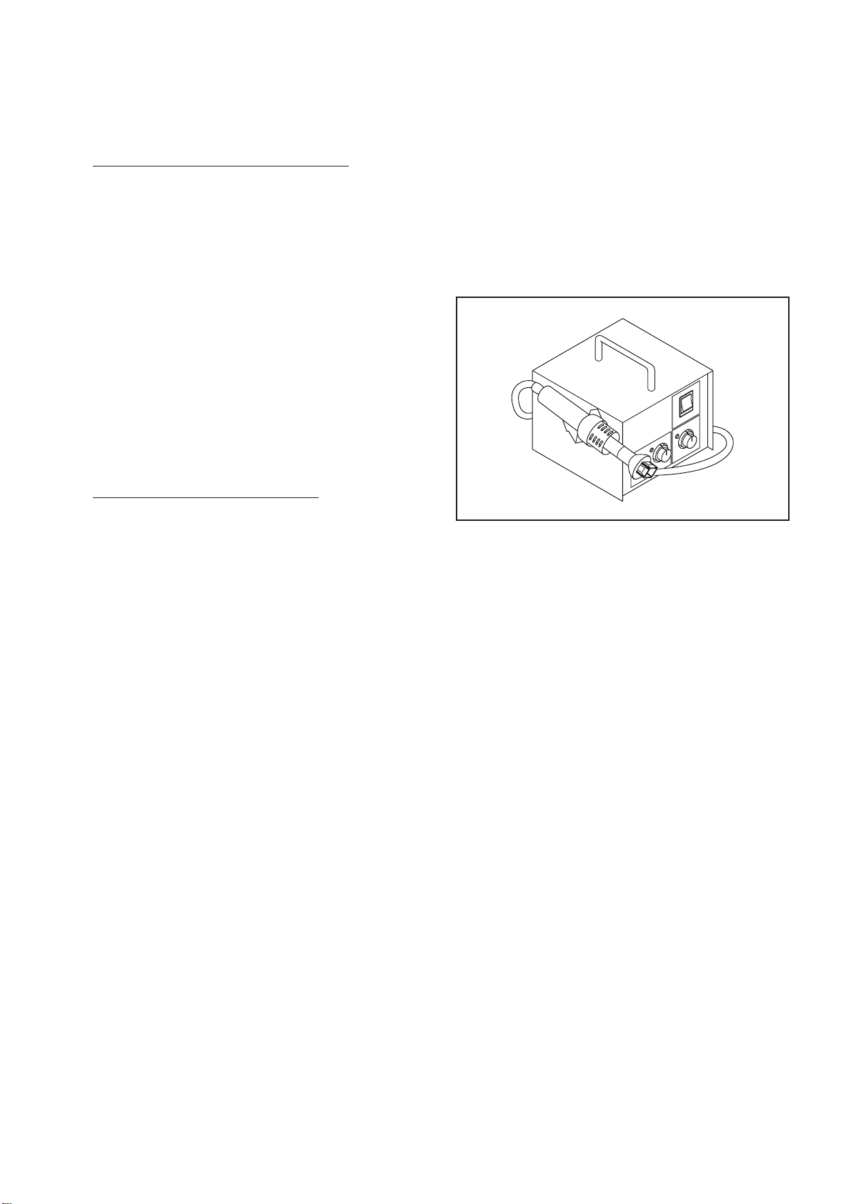
1.1 PCB Locations
VFD Display Board
AMP Board
USB Board
Decoder Board
Ipod Terminal Board
Door Control Board
Touch Board
Main Unit
1.2 General:
Power supply : 220-240V, 50Hz
Voltage(Main Unit) : 27V/1A
Power consumption(Subwoofer) : 40W
Standby power consumption : < 0.3 W
Amplifer : 70W(8Ω) x 2 + 210W(8Ω)
1.3 Radio
Tuning Frequency Range : 87.5MHz - 108MHz
S/N (video unweighted) at 75Ω : ≤71dB
Singal To Noise Ratio : ≥50dB
Search Tuning Sensitivity : 19~35 dBf
RF Signal : < 2.5min
Search Time Digital Tuning System
Stop level (vision carrier) : ≥ 31dBμV
Maximun tuning error during
operation(drift) : ≤ 50 kHz
Maximun tuning error of a recalled
program : ± 22.5 kHz
Modulation : 1kHz
Noise Limlited sensitivity
(26dB Mono) : 22 dBf
Noise Limlited sensitivity
(46dB Stereo) : 52dBf
(Typical 3 minutes)
Door Control Board
AMP/Power Board
Power Control Switch
110/220V(for 55/98
version)
Subwoofer Box
Image Rejection Ratio : ≥25dB
Overall Frequency Response : 63Hz~12.5kHz ±3dB
50dB S/N Sensitivity (Mono),
freq. deviation 75kHz(L,M,H) : ≤23dBf
1.4 Analog Inputs / Outputs
1.4.1 Audio Input Connectors
AUDION IN (AUDIO 1/2) -- AUX IN
Input voltage : 2Vrms max
Input impledance : >10kΩ
AUDION IN (AUDIO 1/2) -- MP3 LINE IN
Input voltage : 1Vrms max
Input impledance : >10kΩ
1.4.2 Video Output Connectors
VIDEO OUT -- CVBS OUT
Output voltage : 700mVpp+10/-15%
Output impledance : 75Ω
S/N on output : ≥ 55dB
1-1
Page 3
Technical Specifications and Connection Facilities
1.5 Digital Inputs/Outputs
1.5.1 COAXIAL DIGITAL IN
LPCM : according IEC 60958-3
MPEG 1, MPEG 2, AC3 : according IEC 61937
DTS : according IEC 61937 +
addendum
1.5.2 USB
Compatibility : USB 2.0
Type of connector
Class support : UMS(USB Mass
File System : FAT12, FAT24, FAT36
1.5.3 HDMI Output
Compatibility
Type of connector : Type A connector
(19 pins)
1.5.4 Sampling Frequency:
MP3 : 32kHz, 44.1kHz, 48kHz
WMA : 44.1kHz, 48kHz
1.5.4 Canstant bit rate:
MP3 : 112 kbps - 320 kbps
WMA : 44 kbps - 192 kbps
1.6 Ipod Docking Component
PHILIPS specified using iPod/iPhone
iPod/ iPhone Voltage : 4.9V ~ 5.02V/1A
: Series A Connector
Storage Class)
: HDMI version 1.3
1.7 Video Performance
1.7.1 SNR
PAL
RGB Y / C
Lumincance: ≥ 55 dB
Chroma: ≥ 55 dB (AM)
≥ 52 dB (PM)
NTSC
Y Pb Pr CVBS
Lumincance: ≥ 55 dB
Chroma: ≥ 54 dB (AM)
≥ 54 dB (PM)
1.7.2 Bandwidth
PAL
RGB CVBS
NTSC
YPbPr CVBS
CVBS
Y / C
Y / C
0.5 to 4 MHz:+1dB/
-2dB
4.8 MHz:-3dB
5.8 MHz:-6dB
Y / C
4.2 MHz:-3dB
5.8 MHz:-6dB
1.7.3 Video Supporting Format
Signal System : PAL / NTSC
Component Video Output:
480i/576i, 480p/576p, 720p, 1080i
HDMI Output:
480p, 576p, 720p, 1080i, 1080p
1-2
Page 4
Technical Specifications and Connection Facilities
1.8 Dimension and Weight
Set Dimension W x H x D : 360 x 190 x 65 mm
Net Weight : 2.2 kg
Subwoofer Dimension W x H x D : 182 x 300 x 345 mm
Net Weight : 5.5 kg
1.9 Laser Output Power & Wavelength
1.9.1 DVD
Output power during reading : 7mW
Output power during writing : 7mW
Wavelength : 645-665nm (at 25 °C)
1.9.2 CD
Output power : 6mW
Wavelength : 770-800nm (at 25 °C)
2.0 Playability
Video Playback
1. Playback Media:
CD-R/CD-RW, DVD+R/+RW,
DVD-R/-RW, DVD-Video, Video
CD/SVCD, DVD+R DL, DVD-R
DL, USB flash drive
2. Compression Formats:
MPEG2, MPEG1, DivX 3.11, DivX
4.x, DivX 5.x, DivX 6.0, MPEG4
Audio Playback
1. Playback Media:
Audio CD, CD-R/RW, DVD+R DL,
DVD+R/+RW, DVD-R/-RW, MP3-
CD, MP3-DVD, USB flash drive,
WMA-CD
2. Compression Format:
Dolby Digital, MP3, MPEG2
Multichannel, PCM, WMA
3. MPEG1 bit rates: 64-384 kbps
and VBR
Still Picture Playback
1. Playback Media: CD-R/RW,
DVD+R DL, DVD+R/+RW, DVDR/-RW, Picture CD, USB Digital
Camera (PTP), USB flash drive
2. Picture Compression Format:
JPEG, JPEG digital camera
photos
3. Picture enhancement: Slideshow
with MP3 playback, Create
albums, Rotate, Slideshow with
music playback, Zoom
x
x
x
x
x
x
x
x
1-3
Page 5
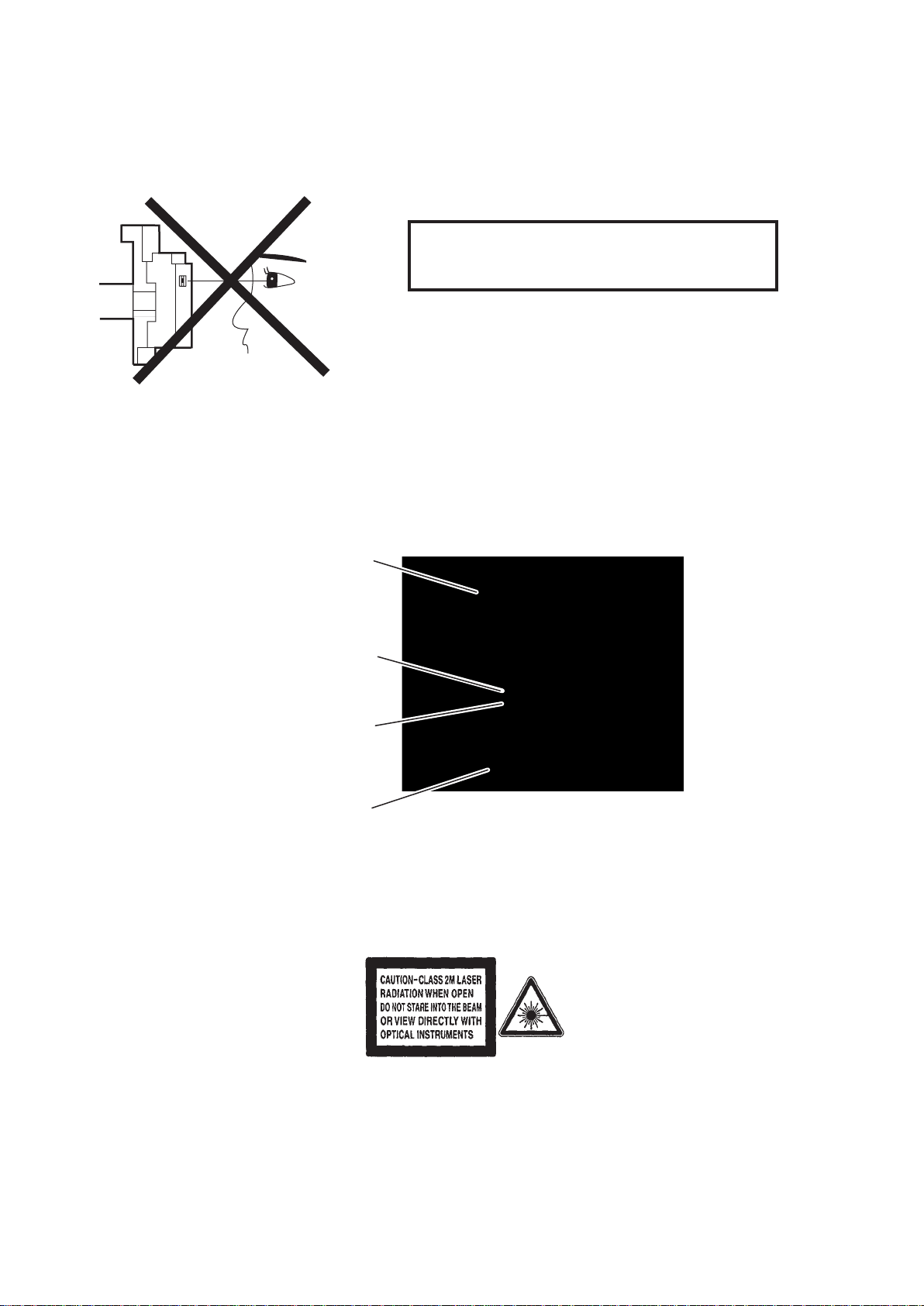
Laser Beam Safety Precautions
This DVD player uses a pickup that emits a laser beam.
Do not look directly at the laser beam coming
from the pickup or allow it to strike against your
skin.
The laser beam is emitted from the location shown in the figure. When checking the laser diode, be sure to keep
your eyes at least 30 cm away from the pickup lens when the diode is turned on. Do not look directly at the laser
beam.
CAUTION: Use of controls and adjustments, or doing procedures other than those specified herein, may result in
hazardous radiation exposure.
Drive Mechanism Assembly
Laser Beam Radiation
Laser Pickup
Turntable
Location: Inside Top of DVDmechanism.
2-1
Page 6

Important Safety Precautions
Important
Read and understand all instructions before you use
your home theater. If damage is caused by failure to
follow instructions, the warranty does not apply.
Safety
Risk of electric shock or fire!
•
Never expose the product and
accessories to rain or water. Never place
liquid containers, such as vases, near the
product. If liquids are spilt on or into the
product, disconnect it from the power
outlet immediately. Contact Philips
Consumer Care to have the product
checked before use.
•
Never place the product and accessories
near naked flames or other heat sources,
including direct sunlight.
•
Never insert objects into the ventilation
slots or other openings on the product.
•
Where the mains plug or an appliance
coupler is used as the disconnect device,
the disconnect device shall remain readily
operable.
•
Disconnect the product from the power
outlet before lightning storms.
•
When you disconnect the power cord,
always pull the plug, never the cable.
Risk of short circuit or fire!
•
Before you connect the product to the
power outlet, ensure that the power
voltage matches the value printed on the
back or bottom of the product. Never
connect the product to the power outlet
if the voltage is different.
Risk of injury or damage to the home theater!
For wall-mountable products, use only
•
the supplied wall mount bracket. Secure
the wall mount to a wall that can support
the combined weight of the product
and the wall mount. Koninklijke Philips
Electronics N.V. bears no responsibility
for improper wall mounting that results in
accident, injury or damage.
•
For speakers with stands, use only the
supplied stands. Secure the stands to
the speakers tightly. Place the assembled
stands on flat, level surfaces that can
support the combined weight of the
speaker and stand.
Never place the product or any objects
•
on power cords or on other electrical
equipment.
If the product is transported in
•
temperatures below 5°C, unpack the
product and wait until its temperature
matches room temperature before
connecting it to the power outlet.
Visible and invisible laser radiation when
•
open. Avoid exposure to beam.
Do not touch the disc optical lens inside
•
the disc compartment.
Risk of overheating!
Never install this product in a confined
•
space. Always leave a space of at least
four inches around the product for
ventilation. Ensure curtains or other
objects never cover the ventilation slots
on the product.
Risk of contamination!
Do not mix batteries (old and new or
•
carbon and alkaline, etc.).
Remove batteries if they are exhausted
•
or if the remote control is not to be used
for a long time.
Batteries contain chemical substances,
•
they should be disposed of properly.
Product care
•
Do not insert any objects other than discs
into the disc compartment.
•
Do not insert warped or cracked discs
into the disc compartment.
•
Remove discs from the disc compartment
if you are not using the product for an
extended period of time.
Only use microfiber cloth to clean the
•
product.
3-1
Page 7
Important Safety Precautions
Disposal of your old product and
batteries
Your product is designed and manufactured
with high quality materials and components,
which can be recycled and reused.
When this crossed-out wheeled bin symbol
is attached to a product it means that the
product is covered by the European Directive
2002/96/EC. Please inform yourself about the
local separate collection system for electrical
and electronic products.
Please act according to your local rules and
do not dispose of your old products with your
normal household waste.
Correct disposal of your old product helps to
prevent potential negative consequences for
the environment and human health.
Your product contains batteries covered by
the European Directive 2006/66/EC, which
cannot be disposed with normal household
waste.
Please inform yourself about the local rules
on separate collection of batteries because
correct disposal helps to prevent negative
consequences for the environmental and
human health.
User manual CD
To read the complete user manual, which
includes information on advanced features, use
the CD supplied with your home theater. For
a printed copy of the complete user manual,
contact Philips Consumer Care in your country.
To access the user manual
Caution
The user manual CD is for PC or Mac only. Do
•
not insert the user manual CD into the disc
compartment of the home theater.
Requirements:
•
A PC (Microsoft Windows
compatible) or Mac (OS X) with
CD-ROM
Adobe Reader
•
1 Insert the user manual CD into the CD-
ROM tray of the PC or Mac.
2 Close the CD-ROM tray.
The user manual screen appears. If the
»
user manual screen does not appear,
skip Step 3 and navigate to the ‘pdf’
folder in the CD-ROM, double-clicking
the PDF of your choice.
3 Click a user manual language.
Acrobat Reader launches, displaying
»
the complete user manual in the
language of your choice.
3-2
Page 8
Safety Check after Servicing
Examine the area surrounding the repaired location for damage or deterioration. Observe that screws, parts, and
wires have been returned to their original positions. Afterwards, do the following tests and confirm the specified
values to verify compliance with safety standards.
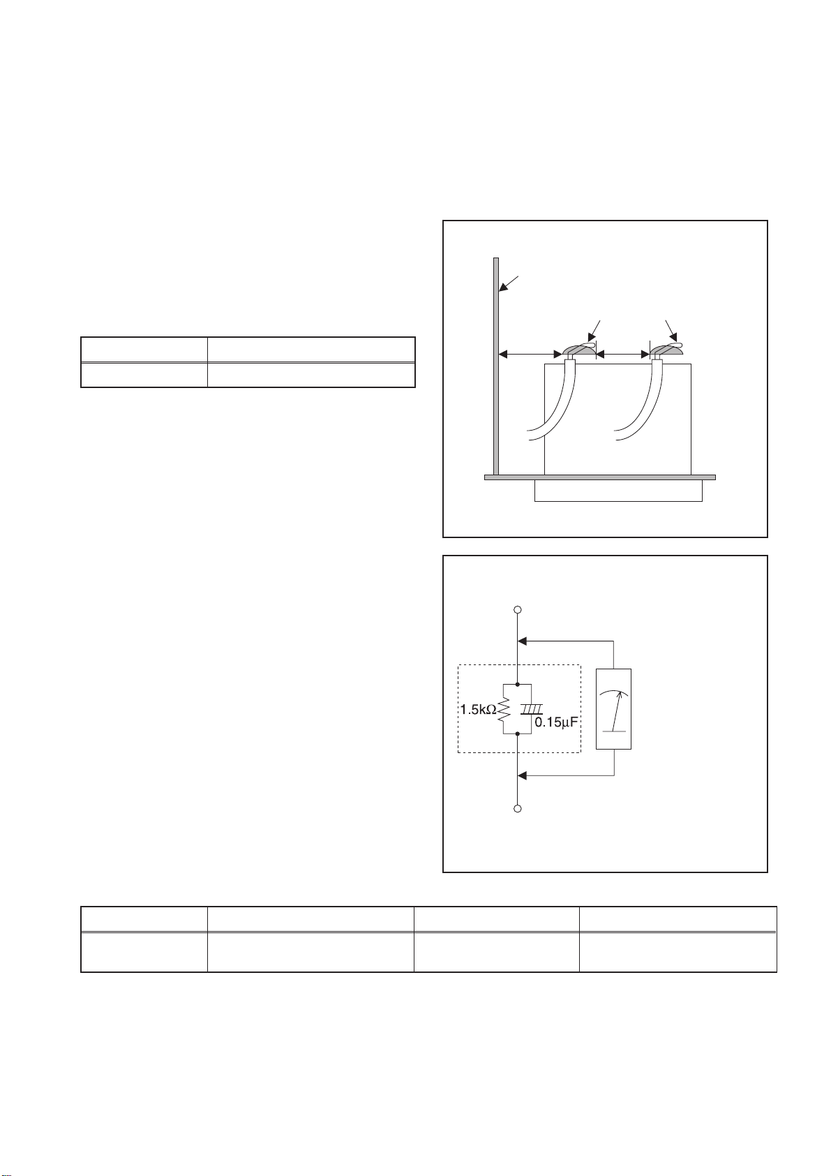
1. Clearance Distance
When replacing primary circuit components, confirm
specified clearance distance (d) and (d’) between
soldered terminals, and between terminals and
surrounding metallic parts. (See Fig. 1)
Table 1: Ratings for selected area
Chassis or Secondary Conductor
Primary Circuit
AC Line Voltage Clearance Distance (d), (d’)
110V~220V ≥ 3.2 mm (0.126 inches)
Note: This table is unofficial and for reference only. Be
sure to confirm the precise values.
2. Leakage Current Test
Confirm the specified (or lower) leakage current
between B (earth ground, power cord plug prongs) and
externally exposed accessible parts (RF terminals,
antenna terminals, video and audio input and output
terminals, microphone jacks, earphone jacks, etc.) is
lower than or equal to the specified value in the table
below.
Measuring Method (Power ON):
Insert load Z between B (earth ground, power cord plug
prongs) and exposed accessible parts. Use an AC
voltmeter to measure across the terminals of load Z.
See Fig. 2 and the following table.
d' d
Fig. 1
Exposed Accessible Part
Z
AC Voltmeter
(High Impedance)
Earth Ground
B
Power Cord Plug Prongs
Table 2: Leakage current ratings for selected areas
AC Line Voltage Load Z Leakage Current (i) Earth Ground (B) to:
110V~220V
Note: This table is unofficial and for reference only. Be sure to confirm the precise values.
0.15 µF CAP. & 1.5 kΩ RES.
Connected in parallel
i ≤ 0.5 mA Peak Exposed accessible parts
4-1
Fig. 2
Page 9
CLASS 1
LASER PRODUCT
Safety Information & Warnings
1 Safety Instructions
1.1 General Safety
Safety regulations require that during a repair:
• Connect the unit to the mains via an isolation transformer.
• Replace safety components, indicated by the symbol
only by components identical to the original ones. Any
other component substitution (other than original type)
may increase risk of fire or electrical shock hazard.
Safety regulations require that after a repair, you must return
the unit in its original condition. Pay, in particular, attention to
the following points:
• Route the wires/cables correctly, and fix them with the
mounted cable clamps.
• Check the insulation of the mains lead for external
damage.
• Check the electrical DC resistance between the mains
plug and the secondary side:
1. Unplug the mains cord, and connect a wire between
the two pins of the mains plug.
2. Set the mains switch to the ‘on’ position (keep the
mains cord unplugged!).
3. Measure the resistance value between the mains
plug and the front panel, controls, and chassis
bottom.
4. Repair or correct unit when the resistance
measurement is less than 1 MΩ.
5. Verify this, before you return the unit to the customer/
user (ref. UL-standard no. 1492).
6. Switch the unit ‘off’, and remove the wire between the
two pins of the mains plug.
1.2 Laser Safety
This unit employs a laser. Only qualified service personnel
may remove the cover, or attempt to service this device (due
to possible eye injury).
,
2 Warnings
2.1 General
• All ICs and many other semiconductors are susceptible to
electrostatic discharges (ESD,
during repair can reduce life drastically. Make sure that,
during repair, you are at the same potential as the mass
of the set by a wristband with resistance. Keep
components and tools at this same potential.
Available ESD protection equipment:
– Complete kit ESD3 (small tablemat, wristband,
connection box, extension cable and earth cable)
4822 310 10671.
– Wristband tester 4822 344 13999.
• Be careful during measurements in the live voltage
section. The primary side of the power supply, including
the heatsink, carries live mains voltage when you
connect the player to the mains (even when the
player is ‘off’!). It is possible to touch copper tracks and/
or components in this unshielded primary area, when
you service the player. Service personnel must take
precautions to prevent touching this area or components
in this area. A ‘lightning stroke’ and a stripe-marked
printing on the printed wiring board, indicate the primary
side of the power supply.
• Never replace modules, or components, while the unit is
‘on’.
2.2 Laser
• The use of optical instruments with this product, will
increase eye hazard.
• Only qualified service personnel may remove the cover or
attempt to service this device, due to possible eye injury.
• Repair handling should take place as much as possible
with a disc loaded inside the player.
• Text below is placed inside the unit, on the laser cover
shield:
). Careless handling
Laser Device Unit
resal rotcudnocimeS : epyT
sAlAaG
Wavelength : 650 nm (DVD)
)DC/DCV( mn 087 :
Output Power : 20 mW
)gnitirw WR+DVD(
Wm 8.0 :
)gnidaer DVD(
Wm 3.0 :
)gnidaer DC/DCV(
Beam divergence : 60 degree
1-2 erugiF
Note: Use of controls or adjustments or performance of
procedure other than those specified herein, may result in
hazardous radiation exposure. Avoid direct exposure to beam.
CAUTION VISIBLE AND INVISIBLE LASER RADIATION WHEN OPEN AVOID EXPOSURE TO BEAM
ADVARSEL SYNLIG OG USYNLIG LASERSTRÅLING VED ÅBNING UNDGÅ UDSÆTTELSE FOR STRÅLING
ADVARSEL SYNLIG OG USYNLIG LASERSTRÅLING NÅR DEKSEL ÅPNES UNNGÅ EKSPONERING FOR STRÅLEN
VARNING SYNLIG OCH OSYNLIG LASERSTRÅLNING NÄR DENNA DEL ÄR ÖPPNAD BETRAKTA EJ STRÅLEN
VARO! AVATTAESSA OLET ALTTIINA NÄKYVÄLLE JA NÄKYMÄTTÖMÄLLE LASER SÄTEILYLLE. ÄLÄ KATSO SÄTEESEEN
VORSICHT SICHTBARE UND UNSICHTBARE LASERSTRAHLUNG WENN ABDECKUNG GEÖFFNET NICHT DEM STRAHL AUSSETSEN
DANGER VISIBLE AND INVISIBLE LASER RADIATION WHEN OPEN AVOID DIRECT EXPOSURE TO BEAM
ATTENTION RAYONNEMENT LASER VISIBLE ET INVISIBLE EN CAS D’OUVERTURE EXPOSITION DANGEREUSE AU FAISCEAU
Figure 2-2
5-1
Page 10

Instruction on halding ESD protection for DVD loader
2.2 Service Hints
CAUTION
CHARGED CAPACITORS ON THE Decoder BOARD MAY DAMAGE THE DRIVE
ELECTRONICS WHEN CONNECTING A NEW DRIVE.THAT’S WHY, BESIDES THE SAFETY
MEASURES LIKE
• SWITCH OFF POWER SUPPLY
• ESD PROTECTION
ADDITIONAL ACTIONS MUST BE TAKEN BY THE REPAIR TECHNICIAN.
The following steps have to be done when replacing the defective loader :
1. Dismantling of the loader to access the ESD protection point if necessary.
2. Solder the ESD protection point*.
3. Disconnect flexfoil cable from the defective loader.
4. Put a paper clip on the flexfoil to short-circuit the contacts (fig.1)
5. Replace the defective loader with a new loader.
6. Remove paperclip from the flexfoil and connect it to the new loader.
7. Remove solder joint on the ESD protection point.
ATTENTION: The laser diode of this loader is protected against ESD by a solder joint which shortcircuits the laserdiode to ground.
*Only applicable for defective loader needed to be sent back to supplier for failure analysis and to support backcharging
evidence.
This is also applicable for all partnership workshops.
For proper functionality of the loader this solder joint must be remove after connection loader to the set.
(ESD protection point is accessible from bottom of the loader)
5-2
Page 11
Standard Notes for Servicing
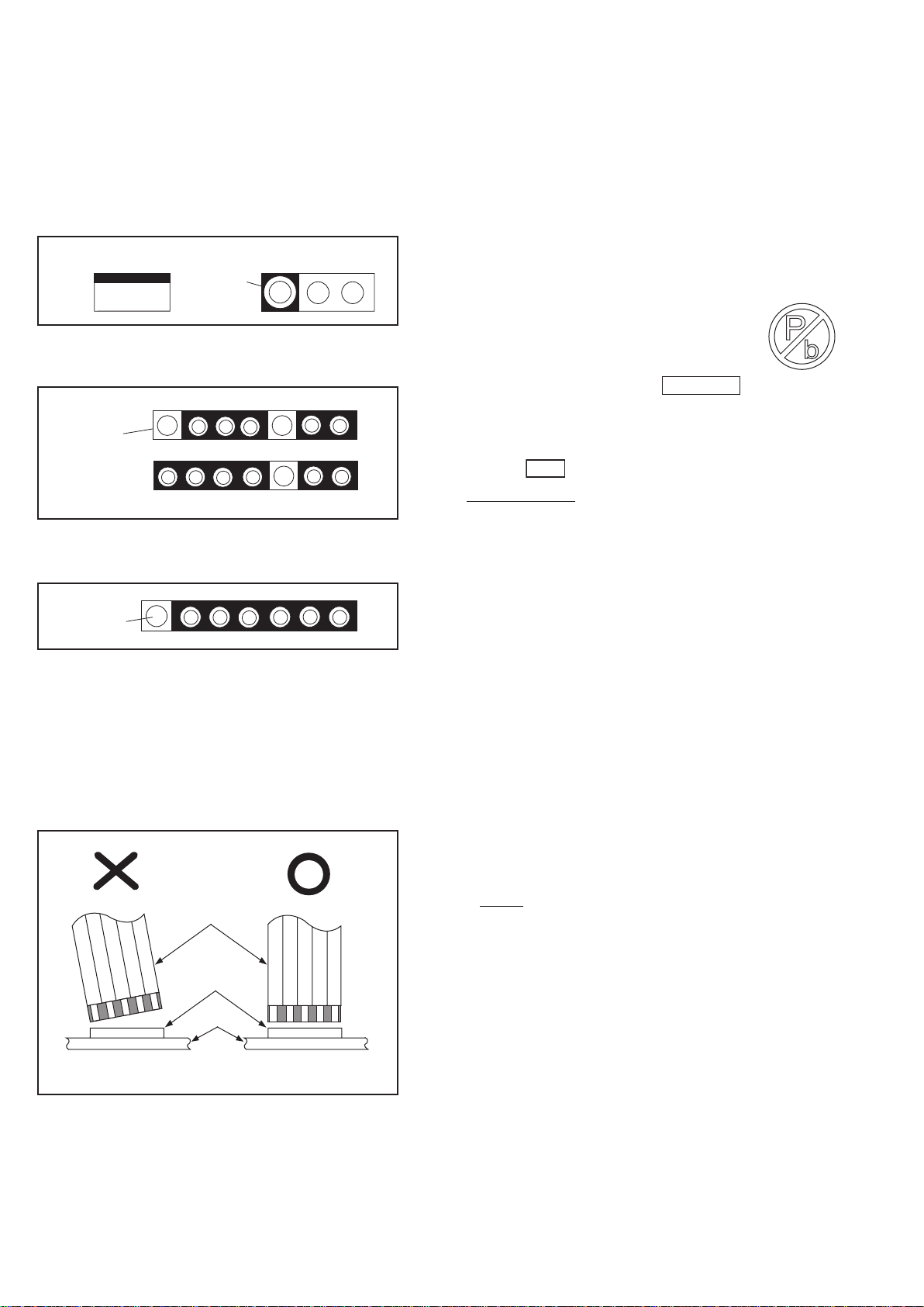
Circuit Board Indications
1. The output pin of the 3 pin Regulator ICs is
indicated as shown.
Top View
Out
2. For other ICs, pin 1 and every fifth pin are
indicated as shown.
Pin 1
3. The 1st pin of every male connector is indicated as
shown.
Pin 1
Input
In
Bottom View
5
10
Instructions for Connectors
1. When you connect or disconnect the FFC (Flexible
Foil Connector) cable, be sure to first disconnect
the AC cord.
2. FFC (Flexible Foil Connector) cable should be
inserted parallel into the connector, not at an
angle.
FFC Cable
Connector
CBA
* Be careful to avoid a short circuit.
Pb (Lead) Free Solder
When soldering, be sure to use the Pb free solder.
Information about lead-free soldering
Philips CE is producing lead-free sets from 1.1.2005
onwards.
IDENTIFICATION
Regardless of special logo (not always
indicated)
One must treat all sets from
onwards, according to the next rule:
Serial Number gives a 14-digit. Digit 5&6 shows the
YEAR, and digit 7&8 shows the WEEK.
So from onwards=from 1 Jan 2005 onwards
Important note : In fact also products of year 2004
must be treated in this way as long as you avoid
mixing solder-alloys (leaded/ lead-free). So best to
always use SAC305 and the higher temperatures
belong to this.
Due to lead-free technology some rules have to be
respected by the workshop during a repair:
• Use only lead-free solder alloy Philips SAC305 with
order code 0622 149 00106. If lead-free solderpaste is required, please contact the manufacturer
of your solder-equipment. In general use of solderpaste within workshops should be avoided because
paste is not easy to store and to handle.
• Use only adequate solder tools applicable for leadfree solder alloy. The solder tool must be able
• To reach at least a solder-temperature of 400°C,
• To stabilize the adjusted temperature at the solder-
• To exchange solder-tips for different applications.
• Adjust your solder tool so that a temperature around
360°C
solder joint. Heating-time of the solder-joint should
not exceed ~ 4 sec. Avoid temperatures above
400°C otherwise wear-out of tips will rise drastically
and flux-fluid will be destroyed. To avoid wear-out of
tips switch off un-used equipment, or reduce heat.
• Mix of lead-free solder alloy / parts with leaded
solder alloy / parts is possible but PHILIPS
recommends strongly to avoid mixed solder alloy
types (leaded and lead-free).
If one cannot avoid or does not know whether
product is lead-free, clean carefully the solder-joint
from old solder alloy and re-solder with new solder
alloy (SAC305).
• Use only original spare-parts listed in the ServiceManuals. Not listed standard-material (commodities)
has to be purchased at external companies.
0501
tip
- 380°C is reached and stabilized at the
1 Jan 2005
6-1
Page 12
Special Information of BGA IC & Flat Pack-IC
•
Special information for BGA-ICs:
- always use the 12nc-recognizable soldering
temperature profile of the specific BGA (for desoldering always use the lead-free temperature
profile, in case of doubt)
- lead free BGA-ICs will be delivered in so-called
'dry-packaging' (sealed pack including a silica gel
pack) to protect the IC against moisture. After
opening, dependent of MSL-level seen on indicatorlabel in the bag, the BGA-IC possibly still has to be
baked dry. (MSL=Moisture Sensitivity Level). This
will be communicated via AYS-website.
Do not re-use BGAs at all.
• For sets produced before 1.1.2005 (except products
of 2004), containing leaded solder-alloy and
components, all needed spare-parts will be available
till the end of the service-period. For repair of such
sets nothing changes.
• On our website
www.atyourservice.ce.Philips.com
information to:
• BGA-de-/soldering (+ baking instructions)
• Heating-profiles of BGAs and other ICs used in
Philips-sets
You will find this and more technical information within
the “magazine”, chapter “workshop news”.
For additional questions please contact your local
repair-helpdesk.
you find more
How to Remove / Install Flat Pack-IC
1. Removal
With Hot-Air Flat Pack-IC Desoldering Machine:
1. Prepare the hot-air flat pack-IC desoldering
machine, then apply hot air to the Flat Pack-IC
(about 5 to 6 seconds). (Fig. S-1-1)
Fig. S-1-1
2. Remove the flat pack-IC with tweezers while
applying the hot air.
3. Bottom of the flat pack-IC is fixed with glue to the
CBA; when removing entire flat pack-IC, first apply
soldering iron to center of the flat pack-IC and heat
up. Then remove (glue will be melted). (Fig. S-1-6)
4. Release the flat pack-IC from the CBA using
tweezers. (Fig. S-1-6)
CAUTION:
1. The Flat Pack-IC shape may differ by models. Use
an appropriate hot-air flat pack-IC desoldering
machine, whose shape matches that of the Flat
Pack-IC.
2. Do not supply hot air to the chip parts around the
flat pack-IC for over 6 seconds because damage
to the chip parts may occur. Put masking tape
around the flat pack-IC to protect other parts from
damage. (Fig. S-1-2)
7-1
Page 13

3. The flat pack-IC on the CBA is affixed with glue, so
be careful not to break or damage the foil of each
pin or the solder lands under the IC when
removing it.
Hot-air
Flat Pack-IC
Desoldering
CBA
Masking
Tape
Machine
Flat Pack-IC
Tweezers
Fig. S-1-2
With Soldering Iron:
1. Using desoldering braid, remove the solder from
all pins of the flat pack-IC. When you use solder
flux which is applied to all pins of the flat pack-IC,
you can remove it easily. (Fig. S-1-3)
With Iron Wire:
1. Using desoldering braid, remove the solder from
all pins of the flat pack-IC. When you use solder
flux which is applied to all pins of the flat pack-IC,
you can remove it easily. (Fig. S-1-3)
2. Affix the wire to a workbench or solid mounting
point, as shown in Fig. S-1-5.
3. While heating the pins using a fine tip soldering
iron or hot air blower, pull up the wire as the solder
melts so as to lift the IC leads from the CBA
contact pads as shown in Fig. S-1-5.
4. Bottom of the flat pack-IC is fixed with glue to the
CBA; when removing entire flat pack-IC, first apply
soldering iron to center of the flat pack-IC and heat
up. Then remove (glue will be melted). (Fig. S-1-6)
5. Release the flat pack-IC from the CBA using
tweezers. (Fig. S-1-6)
Note: When using a soldering iron, care must be
taken to ensure that the flat pack-IC is not
being held by glue. When the flat pack-IC is
removed from the CBA, handle it gently
because it may be damaged if force is applied.
Hot Air Blower
Flat Pack-IC
Desoldering Braid
Soldering Iron
Fig. S-1-3
2. Lift each lead of the flat pack-IC upward one by
one, using a sharp pin or wire to which solder will
not adhere (iron wire). When heating the pins, use
a fine tip soldering iron or a hot air desoldering
machine. (Fig. S-1-4)
Sharp
Pin
Fine Tip
Soldering Iron
Fig. S-1-4
To Solid
Mounting Point
CBA
Tweezers
or
Iron Wire
Soldering Iron
Fig. S-1-5
Fine Tip
Soldering Iron
Flat Pack-IC
Fig. S-1-6
3. Bottom of the flat pack-IC is fixed with glue to the
CBA; when removing entire flat pack-IC, first apply
soldering iron to center of the flat pack-IC and heat
up. Then remove (glue will be melted). (Fig. S-1-6)
4. Release the flat pack-IC from the CBA using
tweezers. (Fig. S-1-6)
7-2
Page 14

Special Information BGA IC & Flat Pack-IC
2. Installation
1. Using desoldering braid, remove the solder from
the foil of each pin of the flat pack-IC on the CBA
so you can install a replacement flat pack-IC more
easily.
2. The “
(See Fig. S-1-7.) Be sure this mark matches the 1
on the PCB when positioning for installation. Then
presolder the four corners of the flat pack-IC. (See
Fig. S-1-8.)
3. Solder all pins of the flat pack-IC. Be sure that
none of the pins have solder bridges.
” mark on the flat pack-IC indicates pin 1.
Example :
Pin 1 of the Flat Pack-IC
is indicated by a " " mark.
Fig. S-1-7
Instructions for Handling Semiconductors
Electrostatic breakdown of the semi-conductors may
occur due to a potential difference caused by
electrostatic charge during unpacking or repair work.
1. Ground for Human Body
Be sure to wear a grounding band (1 MΩ) that is
properly grounded to remove any static electricity that
may be charged on the body.
2. Ground for Workbench
Be sure to place a conductive sheet or copper plate
with proper grounding (1 MΩ) on the workbench or
other surface, where the semi-conductors are to be
placed. Because the static electricity charge on
clothing will not escape through the body grounding
band, be careful to avoid contacting semi-conductors
with your clothing.
<Incorrect>
CBA
Presolder
Flat Pack-IC
Fig. S-1-8
<Correct>
1MΩ
CBA
Grounding Band
1MΩ
CBA
Conductive Sheet or
Copper Plate
7-3
Page 15

Direction of Use
*The following excerpt of the DFU/QSG serves as an introduction to the set.
The Complete Direction for Use can be download in different languages from
the internet site of Philips Customer care Center : www.p4c.philips.com
Your home theater
Congratulations on your purchase, and welcome
to Philips! To fully benefit from the support that
Philips offers, register your home theater at www.
philips.com/welcome.
Main unit
a Display panel
b +/-
Increases or decreases volume.
c SOURCE
Selects an audio/video source for the home
theater.
d ( Standby-On )
Switches the home theater on or to
standby.
e ( Play/Pause )
Starts, pauses or resumes play.
f ( Stop )
•
Stops play.
In radio mode, erases the current •
preset radio station.
g ( Open/Close )
Opens or closes the disc compartment.
h Disc compartment
Remote control
t
s
r
q
p
o
n
m
a ( Standby-On )
•
Switches the home theater on or to
standby.
When EasyLink is enabled, press
•
and hold for at least three seconds
to switch all connected HDMI CEC
compliant devices to standby.
b OPEN/CLOSE
Opens or closes the disc compartment.
a
b
c
d
e
f
g
h
i
j
k
l
8-1
Page 16

Remote Control
Direction of Use
c Source buttons
• DISC: Switches to disc source.
• USB: Switches to USB storage device.
• RADIO: Switches to FM radio.
• AUDIO SOURCE: Selects an audio
input source.
• DOCK for iPod: Switches to Philips
Dock for iPod/iPhone.
d SETUP
Accesses or exits the setup menu.
e ( Navigation buttons )
•
Navigate menus.
In video mode, press left or right to •
fast backward or fast forward.
In radio mode, press left or right to
•
search a radio station; press up or
down to fine tune a radio frequency.
f INFO
Displays information about what is playing.
g Playback buttons
Control playback.
h TREBLE /BASS
Changes treble or bass. Use with +/- .
i Numeric buttons
Selects an item to play.
j AUDIO SYNC
•
Selects an audio language or channel.
Press and hold to synchronize audio •
with video. Use with +/-.
k SOUND MODE
Selects a sound mode.
l REPEAT / PROGRAM
•
Selects a repeat or shuffle mode.
In radio mode, programs radio stations.•
m
ZOOM
Zooms into a video scene or picture.
n HDMI / ANGLE
•
Selects video resolution of HDMI
output from the home theater.
Press and hold to select options for
•
different camera angles.
o SUBTITLE
Selects subtitle language for video.
p SURROUND
Switches to surround sound or stereo
sound.
q +/-
Increases or decreases volume.
r ( Mute )
Mutes or restores volume.
s BACK
Returns to a previous menu screen.
t OK
Con? rms an entry or selection.
8-2
Page 17

Direction of Use
emoh ruoy tcennoC
theater
to a TV and other devices. The basic connections
of the home theater with its accessories are
provided in the Quick Start. For a comprehensive
interactive guide, see www.connectivityguide.
philips.com.
etoN
of the product for identi cation and supply
ratings.
Before you make or change any connections,
•
ensure that all devices are disconnected from
the power outlet.
srotcennoC
srotcennoc ediS
retaeht emoh ruoy tcennoc uoy spleh noitces sihT
mottob ro kcab eht ta etalp epyt eht ot refeR •
srotcennoc kcaB
a TO SUBWOOFER
Connects to the supplied subwoofer.
b SPEAKERS
.srekaeps deilppus eht ot stcennoC
c FM ANTENNA
Connects the FM antenna for radio
reception.
d AUX IN
eht no tuptuo oidua golana eht ot stcennoC
TV or an analog device.
e NI LAIXAOC
Connects to the coaxial audio output on
the TV or a digital device.
f VIDEO OUT
Connects to the composite video input on
the TV.
g HDMI OUT
.VT eht no tupni IMDH eht ot stcennoC
a ( USB )
storage device.
b MP3 LINK
Audio input from an MP3 player.
c Dock for iPod
Connects to a Philips Dock for iPod/iPhone.
(Sold separately)
srotcennoc refoowbuS
BSU a morf tupni erutcip ro oediv ,oiduA
a AC MAINS~
.ylppus rewop eht ot stcennoC
b TO MAIN UNIT
eht ot tcennoC TO
SUBWOOFERconnector on the main unit.
8-3
Page 18

Direction of Use
Connect to the TV
Connect your home theater directly to a TV
through one of the following connectors (from
highest to basic quality video):
a HDMI
b Scart
c Composite video
Option 1: Connect to the TV through
HDMI
Note
If the HDTV has a DVI connector, connect •
using an HDMI/DVI adapter.
If the TV supports EasyLink HDMI CEC,
•
control the home theater and TV with one
remote control (see ‘Use Philips EasyLink’ on
page 13 ).
(Cable not supplied)
TV
Option 3: Connect to the TV through
composite video (CVBS)
Note
The composite video cable or connector might •
be labeled AV IN,VIDEO IN,COMPOSITE or
BASEBAND.
TV
Connect audio from TV or
other devices
Use your home theater to play audio from the
TV or other devices such as a cable box.
Tip
Press • AUDIO SOURCE repeatedly to select
the audio output of your connection.
Option 2: Connect to the TV through
Scart
Use the supplied scart adapter.
TV
Option 1: Connect audio through analog
audio cables
(Cable not supplied)
TV
8-4
Page 19

Option 2: Connect audio through coaxial
cable
Note
The digital coaxial cable or connector might be •
labeled COAXIAL/DIGITAL OUT or SPDIF
OUT.
(Cable not supplied)
TV
Connect a Philips Dock for
iPod/iPhone
Direction of Use
(Philips Dock for iPod/iPhone not supplied)
DOCK for iPod
8-5
Page 20

Cabinet Disassembly Instructions
1. Disassembly Flowchart
This flowchart indicates the disassembly steps to gain
access to item(s) to be serviced. When reassembling,
follow the steps in reverse order. Bend, route, and
dress the cables as they were originally.
[1] Back Cabinet
[2] Decoder Board,
AMP Board
[3] DVD Loader Driver,
VFD Display Board,
[4]USB Board,
Ipod Docking Board
[5] DVD Door
2. Disassembly Method
Note:
(1) Identification (location) No. of parts in the figures
(2) Name of the part
(3) Figure Number for reference
(4) Identification of parts to be removed, unhooked,
unlocked, released, unplugged, unclamped, or
desoldered.
Axx = Screw, CNxx/Jxx/CONxx = Connector
D3.5X12BA is specification of screw.
* = Unhook, Unlock, Release, Unplug, or Desolder
e.g. 7(A01) = seven Screws
ID/
Loc.
No.
[1]
[2]
[3]
[4]
[5]
Part
Back Cabinet
Decoder Board,
AMP Board
DVD Loader
Driver,
VFD Display
Board
USB Board,
Ipod Docking
Board
DVD Door
Remove/*Unhook/
Fig.
No.
D1
D2
D3
D5
Unlock/Release/
Unplug/Desolder
4(A05) D3x12BA,
2(A06) D3x8BA
7(A09) D3x8PA,
4(A07) D3x8FA
5(A08) D3x10BA
4(A10) D2.6x8PWT,
4(A09) D3x8PA,
4(A09) D3x8PA,
D4
12(A02) D2.6x5FT
8(A03) D3x5PT
Removal
Note
A12
A08
A05
A06
Fig. D1
A09
A08
A07
9-1
A09
Fig. D2
Page 21

Fig. D3
Cabinet Disassembly Instructions
A09
A10
Fig. D4
Fig. D5
A09
A02
A03
A03
A02
9-2
Page 22

FLOW CHART NO.1
The power cannot be turned on.
Troubleshooting
Check the Power Switching Adaptor if it has DC 27V output .
Yes
Check the 1st pin which location is U1 if it has DC 27V input
Yes
Check the 2en pin which location is U1 if it has DC 5V output
Yes
Check the Inductor which location is L1
if it has DC 5V
FLOW CHART NO.2
Has not voice form the speaker
Check the 2en pin which location is U8(PT2313)if it has DC 9V
Yes
Check the 1st pin which location is U1 if it has DC 27V input
Yes
Check the 4th pin which location is U1 and U3 on the AMP
Board wether has MUTE signal input
No
No
No
No
No
Try to replace a new AMP Power Board
Replace the D11 & D12 & D13
Replace the IC4
Replace this Inductor
Replace a new one
N o
Check the D10 diode whether has DC 9.1V
Y e s
Check the 2en pin which location is U8 if it has DC 9.1V
N o
Replace the U8 IC(PT2313)
FLOW CHART NO.3
Can not Read Dish
Check the Cable(CON2 and CON3) which connected to the
Loader Driver wether connection is OK?
Yes
Check the L77 & L73 whether has DC 3.3V
Yes
Check the U15 wether has DC 3.3V
No
No
No
Try to connect again
Replace a new one
Replace a new one
10-1
Page 23

Software Upgrading Procedure
1, Download the Software from Philips support
Website:
http://www.philips.com/support.
2, Copy the Software upgrade file into USB device.
A, Connect to TV and Turn on Main Unit
Main unit Screen Display:
TV Screen Display:
C, Press the “OK” on the Remote Control.
D, Software Upgrading, TV Screen Display:
USB and
B, When insert the USB Device with software
Main unit Screen Display:
Meanwhile, the TV Screen Display:
E, After 1 or 2 minute, TV Screen will reset and Display:
Software Upgrade finish.
11-1
Page 24

1, Select the “Menu”, like below show:
2, TV Screen Display:
Software Version Check
2, Select to get the Version information :
11-2
Page 25

Main Unit -- Block Diagram
Touch Board
WT5700
VFDDriver
PT16311
VFD3220
VFD Display Board
USB
IPOD_UART
USB,iPod Board
MCU5V
AudioSwitch
74HC4052D
CEC_IN
CEC_OUT
FM RST
EEPROM
24C02
I2C_MPEG
SPDIF IN
&ADC&DAC
UDA1355H
CN?
4
3
2
1
4P
SERIAL EEPROM
24C02
SDRAM
4M * 16
M12L64164A-7T
FLASH
2M * 8bits
MX29LV160
I2S
FM L&R
+5V
POW&MUTE
SW-IN
GND
Main Chipset
MT1389FXE-S(DTS)
OR
MT1389FXE-S(DTS)
Decoder Board
POW&MUTE
SW-IN
BPF
TL072
AUDIOML/MR
Loader motor driver
CD5954
CEC_OUT
CEC_IN
9.1V
AUDIOPROCESS
PT2313
AUTOMUTE
AMP/Power Board
POWERAMP
TDA8920C
BTL
CEC
BUFFER
9.1V
FL
FR
S L&R
R?
R
BASS
BPF
Open/Close Driver
ESDREJECTOR
CEC
HPD
27V
772
ECOPOWER
MUTE
SPEAKERS
6.5"
8 OHM
Door Detect
28V
STANDBY
SW-IN
S-MUTE
HDMI
Door Control Board
CVBS
TO-MPEG
-27V
7
MCU5V
6
S-MUTE
5
MUTE
4
STANDBY
3
MPEGON
2
GND
1
2.0/7P
TO-MPEG
4
3
2
1
2.0/4P
TO-MPEG
6
5
4
3
2
1
TO-VFD
5
4
3
2
1
2.0/5P
DM-06BXLX-L2
DVDLoader
FR-IN
FL-IN
SW-IN
AGND
GND
M1.8V
M3.3V
M5V
28V
GND
2.5/6P
VFD2
VFD1
-27V
GND
MCU5V
Foryoupick up
CLOSE DOOR
OPENDOOR
FL
FR
SW-IN
MCU5V
MUTE
ECOPOWER
M3.3V
M1.8V
M5V
MCU5V
ECO_POWER
VF2
VF1
-27V
DVD Loader
HPF
NE4558
R?
Q?
9014
4.7K
R?
1K
AMC1117
3.3V
AMC1117
1.8V
VFD
POWER
SUPPLY
E3220DY
PRE-AMP
R?
POW&MUTE
2.2K
MPEGON
SM9435
+5V
AMP Board
9014
S-MUTE
1
NE4558
1
R?
L+
POWERAMP
A
A
Q?
R?
4.7K
47K
TPA3123D2
L-
2
R-
2
R+
R?
2.2K
9014
BTL
MUTE
POWERAMP
TPA3123D2
BTL
SW-IN
GND
MCU5V
POW&MUTE
8 Ohm75Wat 30%
8 Ohm75Wat 30%
P6
28V
P3
GND
P5
P2
5V
P4
P1
1
2
1
2
POW&MUTE
AGND
SW-IN
28V
DCTO DC
AP1501
5V
IR
MPEGON
COAXIAL
AUX
FM RST
ECOPOWER
STANDBY
4052A,B
USBON
USB
IPOD_UART
IPOD_L&R
Si4704
or Si4705(RDS)
FM
M5V
SW-IN
POW&MUTE
IPOD_UART
GND
+5V
MCU
R5R0C028
I2C_MAIN
IPOD_UART
I2C_MAIN
SPDIF_COAXIAL
4052A,B
TO-TOUCH
MCU5V
4
SDA
3
SCL
2
GND
1
4P
TOVFD
IR
5
STB
4
DATA
3
CLK
VF2
VF1
-27V
4P/2.0
DC_5V
CVBS
GND
AGND
2
GND
1
2.0/5P
USB
1
2
3
4
MP3LINE IN
RX
R
TX
L
GND
IR
MCU5V
5V
DP+
DP-
GND
9
8
7
6
5
4
3
2
1
9P2.0
FMAntenna 75OHM
12-1
DC out
+28V
GND
ACIN
POWER1
TOP261
+27V
-27V
+27V
-27V
+28V
Subwoofer Box
200WTHD=30%
+5V
POWER2
12-1
Page 26

Wiring Diagram
wire3
VFD Display Board
VF1
VF2
-27V
GND
STB
+5V
CLK
DAT
GND
REM
wire5
wire4
MCU5V
GND
-27V
VFD1
VFD2
ADD2
GND
ECO_POWER
MUTE
SMUTTE
MCU5V
27V_IN
SWIN
GND
LOUT
GND
ROUT
GND
VCC
AMP Board
wire6
ROUT+
P4
+5V
GND
USBP
USBM
USBM
USBP
GND
wire7
+5V
GND
LIMIT
SL+
SL-
SP+
SP-
Ipod Termial Board
DVD Mechanism
Loader Deriver
wire8
CLK
STB
GND
DATA
REMOTE
wire1
Decoder Board
IPOD_IN_R
NC
IPOD-RX
GND
IPOD-TX
GND
IPOD_IN_L
GND
SW_IN
GND
LOUT
GND
IPOD_5V
GND
GND
GND
ROUT-
+5V
ROUT
27V_IN
MCU5V
J3
S_MUTE
MUTE
ECO-POWER
ADD2
GND
Motor Board
USB Board
Door Control Board
Sub015
Touch Board
Subwoofer Speaker
Subwoofer Box
wire2
AMP/Power Board
Door Control Board
CON1
CON4
AC IN
110/220V Power Control Board
(for /98version)
13-1
13-1
Page 27

Main Unit -- Touch Board Circuit & Layout Diagram
POWER
S5
S7
S8
SOURCE
VOL+
VOLOPEN
STOP
PLAY
1
SI(5)
2
SI(6)
3
SI(7)
4
SI(8)
5
SI(9)
6
SI(10)
7
SI(11)
8
TESET
S6
S9
S10
S11
31
32
30
SI(3)
SI(4)
SI(2)
WT5701-UG321
VSS
INT
VDD
VDD
LED201
LED
R222
100
R204
220
PWM-LED
C203
10U
CN200
PO-LED
R223
25
28
29
26
27
U201
2.2K
LED203 WHI
SI(0)
SI(1)
OUT(10)12OUT(11)
VDD
OUT(8)
OUT(9)
OUT(0)
PWMO(0)
PWMO(1)
OUT(7)
OUT(1)
OUT(2)
OUT(3)
OUT(4)
OUT(5)
SCL
SDA
OUT(6)
24
23
22
21
20
19
18
17
C201
10p
R225 150
R226 150
C202
10p
SCL/STB
SDA
VDD
SDA
SCL/STB
SGND
PWM-LED
CLOSE
OPEN
RESET
INT
1
2
3
4
5
6
7
8
9
10
11
5P
9
10
11
13
15
14
16
14-114-1
Page 28

Main Unit -- VFD Display Board Circuit Diagram
VFD101
HL-D1068W
DC5V
C104
VF1
1
R101
6.81/2W
R110
47K
C105
47uF/16V
104
VF1
2
VF1
G5
G4
G3
G2
G1
NC
4
LED
S13
S146NC
S15
7
5
S14S8S15
40
41
42
43
44
45
46
47
48
49
50
51
52
S1110S1011S912S813S714S6
S12
8
9
S9
S10
S11
S12
S13
G6G7G8
36
37
39
38
G8
G6
G7
G5
G4
G3
G2
G1
Vdd
LED5
LED4(BBE)
LED3(POWER)
LED2(FANCT)
LED1(7507RST)
Vss
OSC
SW2
SW1
SW3
2
1
4
3
15
S6
S7
-27V
35
34
S20/G9
S19/G10
IC100
PT6311
SW4
DOUT
6
5
VEE
DIN
S5
16
S5
DC5V
33
Vdd
IC
7
S417S318S2
S3
S4
32
31
S18/G11
S17/G12
CLK
STB
8
9
S1
19
20
S1
S2
S15
29
30
S15
S16
S12/KS12
S11/KS11
S10/KS10
KEY1
KEY2
10
11
NC
G2
G1
21
22
G4
G3
24
23
25
G1G2G3G4G5G6G7
S13
S14
27
28
S13
S14
S9/KS9
S8/KS8
S7/KS7
S6/KS6
S5/KS5
S4/KS4
S3/KS3
S2/KS2
S1/KS1
Vdd
KEY3
KEY4
12
13
33K
R111
R112 33K
R113 33K
26
26
25
24
23
22
21
20
19
18
17
16
15
14
R114 33K
G5
27
DC5V
G6
28
S12
S11
S10
S9
S8
S7
S6
S5
S4
S3
S2
S1
G7
VF2
31
VF2
VF2
32
R100
6.81/2W
CN102
10
9
8
7
6
5
4
3
2
1
10P2.0
REMOTE
VFD_STB
VFD_DATA
VFD_CLK
V-GND
DC5V
V-GND
-27V
VF2
VF1
JACK501
1
2
3
4
5
6
7
8
9
9P
CN501
1
2
3
4
5
6
7
8
9
9P
G8
29
G8
35-HTS3220-05A1
15-1
R102 4.7K
R103 4.7K
REMOTE
DC5V
VFD_DATA
R104 4.7K
R115
47
C110
47uF/25V
VFD_CLK
VFD_STB
1
2
3
C111
104
S100
REM
GND
Vcc
REMOTE
15-1
Page 29

IC100: PT6311 IC Specification
• 87% Efficiency
• Adjustable Output Voltage
• Internal Short Circuit Protection
• Over-Temperature Protection
• On/Off Control (Ground Off)
• Small SIP Footprint
• Wide Input Range
The PT6310 series is a High-
Performance 2 Amp, 12-Pin SIP
(Single In-line Package) Integrated
Pin-Out Information
Pin Function
Inhibit
1
(30V max)
2 V
Standard Application
VOADJ
V
IN
C1
INH
COM COM
C1 = Optional 1µF ceramic
C
= Required 100µF electrolytic
2
Q1 = NFET
12
V
2,3,4
PT6300
1
5,6,7,8
Q1
9,10,11
OUT
+
C2
Specifications
Characteristics
(Ta= 25° stinUxaMpyTniMsnoitidnoCslobmyS)deton sselnu C
Output Current I
Short Circuit Current I
Input Voltage Range V
Output Voltage Tolerance ∆V
Line Regulation Reg
Load Regulation Reg
Vo Ripple/Noise V
Transient Response t
with Co = 100µF V
Efficiency η Vin=24V, I
Switching Frequency ƒ
Shutdown Current I
Quiescent Current I
Output Voltage V
Absolute Maximum T
Operating Temperature Range
Recommendated Operating T
Thermal Resistance θ
Storage Temperature T
Mechanical Shock Per Mil-STD-883D, Method 2002.3, 1 msec,
Mechanical Vibration Per Mil-STD-883D, Method 2007.2,
* ISR will operate to no load with reduced specifications.
** Input voltage cannot exceed 30V when the inhibit function is used.
Note:
The PT6310 requires a 100µF electrolytic or tantalum output capacitor for proper operation in all applications.
o
sc
in
o
line
load
n
tr
os
o
sc
nl
o
a
a
ja
s
in
3 V
in
4 V
in
5 GND
6 GND
7 GND
8 GND
9 V
out
10 V
out
11 V
out
12 V
out
Over V
Vin = Vo +
Adj
in
0.1 ≤ Io ≤ VA 0.2
Over Vin Range, Io = 2.0 A
Ta = 0°C to +60°C
Over V
in
0.1 ≤ Io ≤ V%5.0±52.0±—A 0.2
V
= V
min, I
in
in
V
o
o
Over Vin and I
V
in
Io = 0A, V
in
Below V
o
V evobAegnaR tnemtsujdA
o
Free Air Convection, (40-60LFM)
V tAegnaR erutarepmeT
= 18V, Io = 2.0A
in
Free Air Convection (40-60LFM) — 30 — °C/W
Half Sine, mounted to a fixture
20-2000 Hz,Soldered in a PC board
Ordering Information
PT6310 = +14.6 Volts
PT6311 = +15.5 Volts
PT6312 = +15.0 Volts
PT6313 = +8.0 Volts
Pkg Style 200
o
o
PT6312 only 500 550 600 kHz
Switching Regulator (ISR) designed to
meet the on-board power conversion
needs of battery powered or other equipment requiring high efficiency and
small size. This high performance ISR
offers a unique combination of features
combining 87% typical efficiency with
open-collector on/off control and adjustable output voltage.
Quiescent current in the shutdown
mode is typically less than 100µA.
PT Series Suffix
Case/Pin
Configuration
Vertical Through-Hole
Horizontal Through-Hole
Horizontal Surface Mount
PT6310 Series
4 — 38** V
o +
— ±1.0 ±2.0 %V
002001—egnahc daol %05 µSec
See Application Notes.
-40 — +85 °C
-40 — +70
— 500
— 10 — G’s
—
(PT1234X)
N
A
C
A0.2—*1.0egnar
kpA—0.5—V5
o
V%5.0±52.0±—egnar
o
o
V%—2±—A0.2 =
o
V%—0.5—toohsrednu/revo
o
%—78—A 0.2 =
zHk008007006segnar
Aµ—001—V51 =
Am—01—V01=
°C
C°521+—04-—
G’s
smarg—5.6———thgieW
15-2
15-2
Page 30

Main Unit -- VFD Display Board Layout Diagram
15-315-3
Page 31

Main Unit -- iPod Terminal, Door Control and USB Board Circuit & Layout Diagam
5
234
1
IPOD
1 5V
2 NC
3 RX
4 GND D
5 AL
6 TX
7 GND A
9 GND
8 AL
8
7
6
9
9P
6 TX
7 GND A
8 AL
9 GND
1 5V
3 RX
2 NC
4 GND D
5 AL
SW301
Touch Switch
35-HTS3220-03A1
1
2
CN301
2P
CN401
4
3
2
1
4P
GND-u
D+
Dvbus
USB
J401
6
GND
5
Shield
4
GND
3
D+
2
D-
1
vbus
16-1 16-1
Page 32

Main Unit -- AMP Board Circuit Diagram
+27V_IN
CN1
CON2X3P(PH=4.2MM)
2
4
6
4750mA
J5
2
1
CON2.54-2
1
3
5
GNDGND
POW/MUTE
R47 4.7K
R50 4.7K
VCC
CB9
0.1uF
MCU5V
2
R308
NC/10K
R45 2.2K
Q2
2N3904
1 3
2
R51
47K
R46 4.7K
R48 4.7K
Q3
1 3
2N3904
POW/MUTE
J3
2
1
CON2.54-2
TP21
VCC
TP24
CE27
+27V_IN
+
L12 FB/1206
CB8
L13 FB/1206
0.1uF
CE28
CD11/220UF35V/D8H12
CB16
0.1uF
TUO_WSV5UCM
CD263/100UF35V/D8H7
27V_IN
+
CB11
0.1uF
CB12
0.1uF
U5
4
AP1501-5V
FB
21
VOUTVIN
GND
SD
3
5
R39
0R/10K
L11
47uH_3A
+
D1
SK34
1 2
CE29
CD263/470UF16V/D8H12
ECO_POWER
MUTE
S_MUTE
D2
1N4148
C30
0.1uF
ECO_POWER
12
R57 5.6K
R60 5.6K
R63
22K
3
1 2
3
R64 10R
Q4
D965,DIP
Q6
D965,DIP
1 2
MCU5V
12
D6
1N4001
C29 0.047uF/dilun
+
CE33 220uF/16V
C31 0.1uF
L14
100uH/0.8A
17-1
VF1
VF2
U9
BZ1
1
2
3
4
5
6
1
6
7
2
7
3
8
4
8
9
5
9
D4 FR104
2
R53 220
R56 220
R59 100
1
D3
6.2V
D5
27V
CE34
+
220uF/35V
-27V
R61
47K
CE75
SW_IN
CD11X/10UF16V/D4H7
R55 1M
C28 100pF
+
2
R62
330
1 3
Q5
2N3904
27V_IN
R54
4.7K
CE32 CD11X/4.7UF16V/D4H7
R58
2.2K
CE35
+
CD11/220UF35V/D8H12
J4
CON2.0-5
+
SW_OUT
27V_IN
SW_IN
GND
MCU5V
ECO_POWER
MUTE
S_MUTE
VF2
1
VF1
2
-27V
3
GND
4
MCU5V
5
27V_IN 2
SW_IN 2
GND 2
MCU5V 2
ECO_POWER 2
MUTE 2
S_MUTE 2
TP26
TP27
TP28
TP29
TP30
17-1
Page 33

Main Unit -- AMP Board Circuit Diagram
ROUT
LOUT
R_OUT
L_OUT
J1
7
6
5
4
3
2
1
CON2.0-7
CE5
2.2UF16V/0603
CE12
2.2UF16V/0603
R21 1K
R24 1K
27V_IN
MCU5V
S_MUTE
MUTE
ECO_POWER
GND
ADD2
+
+
2.2UF16V/0603
C11 0.1uF
C13 0.1uF
TP5
TP6
TP7
TP8
TP9
TP11
TP31
OUT_R+
CE1
+
R2 10K
R3
100K
OUT_L+
CE11
+
2.2UF16V/0603
R14 10K
R16
100K
C19 0.068uF
R28
6.8K
R22
6.8K
R29
24k
J2
CON2.0-5
C27
0.047uF
R1 10K
234
2
3
VSS
CF4558
567
567
R15 10K
C12
R23 24k
0.068uF
567
81
567
VCC1
CF4558
23VSS
234
ROUT
5
4
LOUT
3
GND
2
SW_IN
1
27V_IN
R35
0R/0805
R36
15K
VREF_FILTER
+
CE24
CD11X/100UF35V/D8H7
CE2 2.2UF16V/0603
+
27V_4558
R4 1K
U2
VCC 1
CB1
8 1
0.1uF
R12 1K
CE13 2.2UF16V/0603
+
C14 0.47uF/10% /1UF
27V_4558
U4
CB4
0.1uF
C20 0.47uF/10% /1UF
VREF_FILTER
TP32
TP33
TP34
TP35
27V_4558
CE23
+
CHIP CAP EL 100UF-35V M 8*7
R37
15K
OUT_R-
VREF_FILTER
OUT_L-
R_OUT
L_OUT
27V_IN
+
CE4
CD263/470UF35V/D10H16
R5 4.7K
ECO_POWER
+
CE6
R6
47K
47UF
R10 4.7K
MUTE
R11
10K/NC
OUT_L+
OUT_L-
OUT_R+
OUT_R-
HOLE/GND
H4
H2
1
1
HOLE/GND
1
1
2
2
3
3
4
4
5
5
2
2
3
3
4
4
5
5
9
9
8
8
7
7
6
6
9
9
8
8
7
7
6
6
HOLE/GND
H5
H6
1
1
HOLE/GND
1
1
2
2
3
3
4
4
5
5
2
2
3
3
4
4
5
5
9
9
8
8
7
7
6
6
9
9
8
8
7
7
6
6
R31 4.7K
R32 4.7K
R17 4.7K
R18 4.7K
R19
3.9K
R333.9K
C25
470pF
C9
470pF
R343.9K
SW_IN
LOUT
+
CE9
1u/50V
R309 470
R310 8.2K
C26
470pF
R203.9K
CB17
0.47uF
STANDBY1
MUTE1
CE7 CD11X/4.7UF16V/D4H7
CE8 CD11X/4.7UF16V/D4H7
C10
470pF
CE18 CD11X/4.7UF16V/D4H7
CE19 CD11X/4.7UF16V/D4H7
+
CE36
10uF
+
CE37
0.047uF
+
+
27V_IN
+
CE17
CD263/470UF35V/D10H16
STANDBY1
MUTE1
+
+
D7 1N60
1
D9
1N60
1 2
D8 1N60
1 2
D10
1N60
1 2
CE10
1uF
CE20
1uF
CE14
1uF
CE21
1uF
CB3
0.1uF
CB6
0.1uF
2
+
CE38
47u/50V
L1 FB/DIP
U1
1
PACCL
2
SD
3
PVCCL
4
MUTE
5
LIN
6
RIN
7
BYPASS
8
GND
9
GND
10
PVCCR
11
VCLAMP
12
PVCCR
CE15
1uF
L6 FB/DIP
U3
1
PACCL
2
SD
3
PVCCL
4
MUTE
5
LIN
6
RIN
7
BYPASS
8
GND
9
GND
10
PVCCR
11
VCLAMP
12
PVCC PGNDR
CE22
1uF
ADD2
R312
CB15
0.1uF
150K
30
30
PGNDL
PGNDL
LOUT
AVCC
AVCC
GAIN0
TPA3123D2
GAIN1
ROUT
PGNDR
PGNDR
30
30
PGNDL
PGNDL
LOUT
AVCC
AVCC
GAIN0
TPA3123D2
GAIN1
ROUT
PGNDR
+
CE3
CD263/470UF35V/D10H16
2526272829
2526272829
24
23
22
21
BSL
20
19
18
17
16
BSR
15
14
13
+
CE16
CD263/470UF35V/D10H16
2526272829
2526272829
24
23
22
21
BSL
20
19
18
17
16
BSR
15
14
13
C1 0.22uF/0805
R8100K
R9 100K
C5 0.22uF/0805
CB2
0.1uF
C15 0.22uF/0805
R26100K
R27 100K
C21 0.22uF/0805
CB5
0.1uF
Y1
Y2
Y3
Y4
L3 FB/100/5A
C3
220pF
L5 FB/100/5A
C7
220pF
L8 FB/100/5A
C17
220pF
L10 FB/100/5A
C22
220pF
L2 33UH/3.5A LHP1014
R7
5.6R
C4
1800pF
L4 33UH/3.5A LHP1014
R13
5.6R
C8
1800pF
L7 33UH/3.5A LHP1014
R25
5.6R
C18
1800pF
L9 33UH/3.5A LHP1014
R30
5.6R
C24
1800pF
27V_IN
SW_IN
GND
MCU5V
MUTE
ECO_POWER
S_MUTE
C2
0.47uF/dilun
C6
0.47uF/dilun
C16
0.47uF/dilun
C23
0.47uF/dilun
SPK_ROUT+
SPK_ROUT-
27V_IN 1
SW_IN 1
GND 1
MCU5V 1
MUTE 1
ECO_POWER 1
S_MUTE 1
TP2
TP1
SPK_LOUT+
SPK_LOUT-
TP4
TP3
1
2
3
4
5
6
P2
PRC-101A
1
2
3
4
5
6
P1
PRC-101A
17-2
17-2
Page 34

LS
HS
LS
HS
OSC/RAMP
MUTE
CONTROL
BYPASS
AV
CONTROL
CONTROL
BIAS
THERMAL
SC
DETECT
SC
DETECT
AVDD
AVCC
LIN
RIN
MUTE
BYPASS
GAIN1
GAIN0
SD
BSL
PVCCL
LOUT
PGNDL
VCLAMP
BSR
PVCCR
ROUT
PGNDR
VCLAMP
VCLAMP
AVDD
AVDD
AVDD/2
AVDD
AVDD
AVDD/2
REGULATOR
AGND
+
-
+
-
U1,U3 -- TPA3123D2 IC Specification
TPA3123D2 BLOCK DIAGRAM
PWP (TSSOP) PACKAGE
(TOP VIEW)
SD
NAME
TERMINAL
24-PIN
(PWP)
2 I
PVCCL
SD
PVCCL
MUTE
LIN
RIN
BYPASS
AGND
AGND
PVCCR
VCLAMP
PVCCR
1
2
3
4
5
6
7
8
9
10
11
12
Table 1. TERMINAL FUNCTIONS
I/O/P DESCRIPTION
Shutdown signal for IC (low = disabled, high = operational). TTL logic levels with compliance to
AVCC
24
23
22
21
20
19
18
17
16
15
14
13
RIN 6 I Audio input for right channel
LIN 5 I Audio input for left channel
GAIN0 18 I Gain select least-significant bit. TTL logic levels with compliance to AVCC
GAIN1 17 I Gain select most-significant bit. TTL logic levels with compliance to AVCC
MUTE 4 I
Mute signal for quick disable/enable of outputs (high = outputs switch at 50% duty cycle, low =
outputs enabled). TTL logic levels with compliance to AVCC
BSL 21 I/O Bootstrap I/O for left channel
PVCCL 1, 3 P Power supply for left-channel H-bridge, not internally connected to PVCCR or AVCC
LOUT 22 O Class-D 1/2-H-bridge positive output for left channel
PGNDL 23, 24 P Power ground for left-channel H-bridge
VCLAMP 11 P Internally generated voltage supply for bootstrap capacitors
BSR 16 I/O Bootstrap I/O for right channel
ROUT 15 O Class-D 1/2-H-bridge negative output for right channel
PGNDR 13, 14 P Power ground for right-channel H-bridge.
PVCCR 10, 12 P Power supply for right-channel H-bridge, not connected to PVCCL or AVCC
AGND 9 P Analog ground for digital/analog cells in core
AGND 8 P Analog ground for analog cells in core
BYPASS 7 O
Reference for preamplifier inputs. Nominally equal to AVCC/8. Also controls start-up time via
external capacitor sizing.
AVCC 19, 20 P High-voltage analog power supply. Not internally connected to PVCCR or PVCCL
Thermal pad Die pad P
Connect to ground. Thermal pad should be soldered down on all applications to properly
secure device to printed wiring board.
17-3 17-3
PGNDL
PGNDL
LOUT
BSL
AVCC
AVCC
GAIN0
GAIN1
BSR
ROUT
PGNDR
PGNDR
Page 35

Main Unit -- AMP Board Layout Diagram
17-4
17-4
Page 36

Main Unit -- Decoder Board Circuit Diagram
CON3
H24 SMD0.5
25
26
C111
150pF
STBY
470UF6.3V/D8H7
CE72
R236
20K
24
23
22
21
20
19
18
17
16
15
14
13
12
11
10
9
8
7
6
5
4
3
2
1
R240
0
+
SONY313
GND
LD_DVD
AVCC1
MDI1
LD_CD
VR_DVD
VR_CD
E
AVCC1
V20
GND
F
B
A
RFO
IOA
D
C
TT+
F+
F-
R228
1/0805
SL+
SL-
MO_VCC
CB95
0.1uF
Q18
2SK3018
R229
1/0805
STBY1
R241
10K
R216
100K
1
R222
100
32
T+
FMSO
TRSO
V1P4
T-
1 3
32
CB93
0.1uF
CB96
0.1uF
R217
10K
R220 10K
2
Q17
2N3904
Q19
2SK3018
R223
100
15
16
17
18
19
20
21
30
22
23
24
25
26
27
28
R221
100K
1
CB92
0.1uF
U14 CD5954
VOTK+
VOTKVOLD+
VOLDPGND
VNFTK
PVCC2
PREGND
VINLD
CTK2
CTK1
VINTK
BIAS
STBY
VCC
IOA
CE50
+
220UF/10V
L66
10uH/SMD
L67
10uH/SMD
VOFC+
VOFC-
VOSL+
VOSL-
PGND
PVCC1
VCC
G1G2
VNFFC
VOSL
VINSL-
VINSL+
CF2
CF1
VINFC
CE55
220UF/10V
L70
FB
14
13
12
11
10
9
8
29
7
6
5
4
3
2
1
F+
CB91
TP70
0.1uF
CON2
CON2.0-6
VCC
LDO2
Q20
8550/DIP
2
1 3
13
SP-A
SP+
R231
1/0805
R230
1/0805
300mA
R234
V1P4
FOSO
+
10K
CB97
0.1uF
F-
R225
4.7
R226
4.7
2
Q23
8550/DIP
L68
-1206
2.2
欧
R237
20K
VCCMO_VCC
R235
20K
CE52
47UF/16V
+
+
CE53
47UF/16V
C113
150pF
DMSO
CE51
+
+
10UF/16V
R224
10K
R227
10K
CE54
10UF/16V
Q21
2N3906
2
1 3
13
2
Q22
2N3906
LDO1
TP47
SP-
6
SP+
5
LIMIT
4
3
SL-
2
SL+
1
TP48
R238
150K
SP-A
TP49
TP50
RFV33
CB94
0.1uF/NC
C110
2200pF
R232
680K
R218
1/0805
SP-
R239
150K
SP-A
DV33
R233
680K
C112
2200pF
R215
10K
R219
33
UP3_0
OPO
OP-
OP+
V1P4
IOA
LDO2
LDO1
MDI1
E
V20
F
B
A
RFO
D
C
FMSO
TRSO
STBY
FOSO
DMSO
UP3_0
OPO
OPOP+
V1P4
GND
DV33
RFV33
VCC
IOA 2
LDO2 2
LDO1 2
MDI1 2
E 2
V20 2
F 2
B 2
A 2
RFO 2
D 2
C 2
FMSO 2
TRSO 2
STBY 2
FOSO 2
DMSO 2
UP3_0 2
OPO 2
OP- 2
OP+ 2
V1P4 2
GND 2,3,4,5
DV33 2,3,4,5
RFV33 2
VCC 2,4,5
18-1 18-1
Page 37

Main Unit -- Decoder Board Circuit Diagram
RFV33
L46
DV33
CE44
+
10uF/25V
D25
1N4148
1 2
R204
1K
R206
10K
CB69
0.1uF
RFV33
V2P8
2
C107
0.01UF
FB
+
CE40
10uf/10v/0805
R202
1K
RESET
Q14
2N3904
1 3
R182
6.8
CB70
0.1uF
V18
L53 FB/0603
V18 F
FOSO
TRSO
FMSO
DMSO
C101
C100
CB85
330pF
330pF
0.1uF
R203
10K
URST#
DVD3.3V
C73
0.01UF
CB66
0.1uF
V20
CE41
+
22UF/6.3V/0805
RFV18
CB76
0.1uF
R192 20K
R193 18K
R194 15K
R195 10K
C102
0.015uF
L62
FB
L64
FB
RFVDD3
C74
2200pF
PLLVDD3
+
CE38
100UF/16V
FOO
TRO
FMO
DMO
V1P4
+
CE46
22UF/6.3V/0805
+
CE49
100UF/16V
CB71
0.1uF
V1P4
+
CE42
22UF/6.3V/0805
V18
89S_3V3
DV33
R180
100K
Y8
27MHz
CB73 0.1uF
R185 15K
C92 1uF/16V
MDI1
MDI2
CB80
0.1uF
USBP
R189 0
R190 0
USBM
A2
A3
A4
A5
A6
A7
A8
A18
A19
XO
R179
0
C72
27pF
C
B
A
D
V2P8
V20
V1P4
TEZISLV
OPO
OPOP+
DMO
FMO
TRO
FOO
USB_V33
USB_V18
A_MUTE
IOA
XI
R178
0
L45
2.7uH/NC
C70
1000pF/NC
C95
L56
4.7uF/6.3V
FB
89S_3V3
CB82
0.1uF
L57
FB/0603
L58 FB/0603
V18
C98 10pF
USB_P
USB_M
C99 10pF
89S_3V3 RFV33
L61
1R/0805
CB87
0.1uF
CB89
0.1uF
L47
FB
C
B
A
C90 1uF/16V
D
RFO
C93 120pF/NC
RFV33
RFV33
CB77
0.1uF
CB81
0.1uF
C96
4.7uF/6.3V
C97
10uF/10V/0805
C71
27pF
C88 1uF/16V
C89 1uF/16V
C91 1uF/16V
E
LDO2
LDO1
R191 5.1K
CB83
0.1uF
V18
+
CE47
22UF/6.3V/0805
RFVDD3
USB_P
USB_M
C69 1000pF
JITFO
R181 750K
V1P4
CB59 0.1uF
20pF
C75
R183 100K
CB65 0.1uF
1000pF
C79
RFVDD3
RFVDD3
JITFN
JITFO
C82 0.047uF
C81 0.033uF
256
255
254
257
258
U13
OSP
CB72 0.1uF
MARK1
MARK2
RFGND
1
OSN
2
RFGC
3
IREF
4
AVDD3
5
AGND
6
DVDA
7
DVDB
8
DVDC
9
DVDD
10
DVDRFIP
11
MA
12
MB
13
MC
14
MD
15
SA
16
SB
17
SC/TNI
18
SD/TPI
19
MDI1
20
MDI2
21
LDO2
22
LDO1
23
SVDD3
24
CSO/RFOP
25
RFLVL/RFON
26
SGND
27
V2REF
28
V20
29
VREFO
30
FEO
31
TEO
32
TEZISLV
33
OP_OUT
34
OP_INN
35
OP_INP
36
DMO
37
FMO
38
TROPENPWM
39
PWMOUT1/_ADIN0
40
TRO
41
FOO
42
AGND18_DMPLL
43
AVDD18_DMPLL
44
USB_DP
45
USB_DM
46
VDD33_USB
47
VSS33_USB
48
PAD_VRT
49
VDD18_USB
50
VSS18_USB
51
USB_XTALO/GPIO15
52
USB_XTALI/GPIO14
53
FG/GPIO16
54
IOA22/GPIO18
55
DVDD18
56
IOA2
57
IOA3
58
IOA4
59
IOA5
60
IOA6
61
IOA7
62
HIGHA0
63
IOA18
64
IOA19
DVDD33
IOWR
6566676869707172737475767778798081828384858687888990919293949596979899
89S_3V3
A16
PWR#
CB88
0.1uF
RXD
TxD
C83 0.047uF
CB68 0.1uF
253
252
HRZFC
CRTPLP
A16
HIGHA7
A14
A15
DV33
PLLVDD3
251
250
249
248
247
246
245
244
243
242
241
JITFN
LPFIP
LPFIN
LPFOP
LPFON
PLLVSS
RFVDD3
ADCVSS
RFRPAC
RFRPDC
PLLVDD3
ADCVDD3
HIGHA6
HIGHA5
HIGHA4
HIGHA3
HIGHA2
HIGHA1
IOA20
IOCS
IOA1
IOOE
AD0
AD1
PCE#
A13
PRD#
A20
AD1
A10
A12
AD0
A11
A9
A1
CON1
CON2.0-4
红色
1
2
3
4
JITFN
C7610uF/10V/0805
+
CE39 470UF/6.3V
C80 4.7uF/6.3V
XO
XI
RFV18
RFV18
240
239
238
237
236
235
234
JITFO
XTALI
XTALO
RFVDD18
RFGND18
SADCVSS18
AL
ADACVDD
ADACVDD
AVCM
AR
233
232
231
230
229
228
227
226
225
224
223
222
AL
AR
ALS
CH7
CH8
AVCM
CENTER
ADACVSS3
ADACVDD3
ADACVDD1
ADACVDD2
SADCVDD18
MT1389S
MT1389FE-SEAL
DVSS18
AD2
AD3
AD4
AD5
AD6
IOA21/GPIO17
ALE
AD7
DVSS33
A17
IOA0
DVDD18
UWR
URD
DVDD33
UP1_2/GPIO19
UP1_3/VSCK
AD2
A21
AD4
AD7
AD6
AD3
AD5
R200 33/NC
A17
A0
SSCL
V18
R205 0
SCL_DVD SSCL
R207 0
TX0+
TX0+ 4
TX0-
TX0- 4
TX1+
TX1+ 4
TX1-
TX1- 4
TX2+
TX2+ 4
TX2-
TX2- 4
TXC+
TXC+ 4
TXC-
TXC- 4
89S_HPD
ADACVDD
L42 150uH/DIP
APLLVDD3
L43 47uH/DIP
DACVDD3
L44 FB
FS
DACVDD3
VREF
197
196
195
194
193
FS
VREF
DACVDDC
TS_DATA1
TS_DATA0
DACVSSC
DACVDDB
DADVSSB
DACVDDA
DACVSSA
AGND18_TX0
AVDD18_TX0
AGND18_TX1
AVDD18_TX1
AGND18_TX2
AGND33_TX
EXT_CAP
AVDD33_TX
AVDD33_VPLL
EXT_RES
AGND33_VPLL
GPIO8_HPLG
GPIO7_DDC_CLK
GPIO6_DDC_DA
GPIO20/SD_CMD
RD13
RD12
RD11
RD10
RD9
124
125
126
127
128
DQ10
DQ13
DQ11
DQ12
DQ9
P4
CON2.0-4
CB52
0.1uF
DVDD18
GPIO5
GPIO4
DVDD33
DVSS33
DVDD33
DVDD18
DQM1
DVDD33
4
3
2
1
CVBS
TX2P
TX2N
TX1P
TX1N
TX0P
TX0N
TXCP
TXCN
RA11
RCLK
RA10
RWE
RA4
RA5
RA6
RA7
RA8
RA9
CKE
RA3
RA2
RA1
RA0
BA1
BA0
RCS
RAS
CAS
RD8
USBP
USBM
+
CE37
10uF/25V
R184
2K
Y
C
G
B
R
TP71
CB67
0.1uF
89S_3V3
192
191
190
189
188
187
186
185
184
183
182
181
180
179
178
177
176
175
174
173
172
171
170
169
168
167
166
165
164
163
162
161
160
159
158
157
156
155
154
153
152
151
150
149
148
147
146
145
144
143
142
141
140
139
138
137
136
135
134
133
132
131
130
129
TP42
+5V_USB
C108
100pF
CB49
CE36
+
0.1uF
100UF/16V
C771500pF
C78
10uF/10V/0805
V18
TP40
TP39
221
220
219
218
217
LFE
ARS
APLLVSS
APLLCAP
ADACVSS1
ADACVSS2
UP1_4/VSTB
UP1_5/VSDA
UP1_6/SCL
UP1_7/SDA
UP3_0
UP3_1
100
101
102
103
104
R201 33/NC
SDA_DVD
UP3_0
SCL_DVD
SSDA
C106 100pF
C105 100pF
DV33
89S_3V3
TP41
STBY
APLLVDD3
TRIN
GPIO12
216
215
214
213
212
211
210
209
208
GPIO9
GPIO12
GPIO11
GPIO10
DVDD18
TS_PWM
APLLVDD
TS_ERROR
SPDIF/GPIO23
UP3_4/RXD
UP3_5/TXD
ICE
PRSTIRGPIO22/SDD0/INT
DQM0
GPIO21/SD_CLK
106
TXD
R211
1K
RD7
107
108
109
110
111
112
113
URST#
DQM0
DQ7
CB86
NC/0.1uF
R212
1K
SCL_DVD
SDA_DVD
105
RXD
SSDASDA_DVD
CB51
CB50
0.1uF
0.1uF
MDATA_IN
MLRCK_IN
MBCK_IN
MMCLK_IN
TS_DATA2
207
206
205
204
203
202
201
200
199
198
TS_CLK
DVDD33
TS_SYNC
TS_VALID
TS_DATA7
TS_DATA6
TS_DATA5
TS_DATA4
TS_DATA3
TS_DATA2
RD6
RD5
RD4
RD3
DVDD33
RD2
RD1
RD0
RD15
114
115
DQ6
DQ5
RD14
116
117
118
119
120
121
122
123
DQ15
DQ14
DQ4
DQ2
DQ0
DQ1
DQ3
V18
DACVDD3
CVBS
DACVDD3
TX2+
TX2-
TX1+
TX1-
TX0+
TX0-
TXC+
TXC-
C94 5600pF
AV33
R187 2.55K 1%
R188 0
GPIO7
GPIO6
GPIO5
MA4
MA5
MA6
MA7
MA8
MA9
MA11
DCKE
DCLK
MA3
MA2
MA1
MA0
MA10
BA1
BA0
CS#
RAS#
CAS#
WE#
DQM1
DQ8
TP43
TP44
L63
FB/600/0603
89S_3V3
89S_HPD
C109
100pF
CB74
0.1uF
+
CE48
220UF/10V
CB75
0.1uF
CB78
0.1uF
FB/0603
L52
L54 FB
L55 FB
CB79
0.1uF
Q16
2N3904
V18
R208
0/NC
Q15
CES2307
1 3
CES2302/NC
3
R210
1K
2
89S_3V3
CB53
CB57
CB56
CB55
CB54
0.1uF
CB60
0.1uF
MMCLK_IN
MBCK_IN
MLRCK_IN
MDATA_IN
C84
100pF
R186
0/0805
Q12
1
89S_3V3
VCC
2
CVBS
VCC
R209
47K
R213
4.7K
USB_ON
R214
CB90
10K
0.1uF
CB61
0.1uF
R197
160 1%
C85
100pF
0.1uF
CB62
0.1uF
C86
100pF
C87
200PF
VCC
0.1uF
V18
CB63
0.1uF
R301 0
R302 0
R303 0
R304 0
1.8uH/0603
L59
C103
47pF
L60 FB
0.1uF
CB64
0.1uF
CB58
0.1uF
0.1uF
MCLK_IN
BCK_IN
LRCK_IN
DATA1_IN
CE43 100UF/16V
+
R198
C104
2.2K
47pF
+5VV
CE45
+
22UF/16V
R196
3.3K
+5VV
CB84
0.1uF
Q13
2
2N3904
1 3
100UF/16V
R199
75 1%
TS_DATA2
A[0..21]
AD[0..7]
PRD#
PWR#
PCE#
MA[0..11]
DQ[0..15]
BA[0..1]
GPIO[5..7]
DQM[0..1]
DCLK
DCKE
CAS#
RAS#
WE#
CS#
SCL_DVD
SDA_DVD
SSCL
SSDA
AL
AR
A_MUTE
UP3_0
V1P4
OP+
OPOPO
IOA
STBY
V20
MDI1
RFO
E
F
B
A
C
D
FOSO
TRSO
FMSO
DMSO
LDO2
LDO1
USB_ON
TRIN
MCLK_IN
LRCK_IN
BCK_IN
DATA1_IN
V18
DVD3.3V
VCC
GND
RFV33
DV33
89S_3V3
CVBS_OUT
URST#
CE64
+
89S_HPD 5
TS_DATA2 4
A[0..21] 3
AD[0..7] 3
PRD# 3
PWR# 3
PCE# 3
MA[0..11] 3
DQ[0..15] 3
BA[0..1] 3
GPIO[5..7] 4
DQM[0..1] 3
DCLK 3
DCKE 3
CAS# 3
RAS# 3
WE# 3
CS# 3
SCL_DVD 3
SDA_DVD 3
SSCL 5
SSDA 5
AL 5
AR 5
A_MUTE 5
UP3_0 1
V1P4 1
OP+ 1
OP- 1
OPO 1
IOA 1
STBY 1
V20 1
MDI1 1
RFO 1
E 1
F 1
B 1
A 1
C 1
D 1
FOSO 1
TRSO 1
FMSO 1
DMSO 1
LDO2 1
LDO1 1
USB_ON 5
TRIN 5
MCLK_IN 5
LRCK_IN 5
BCK_IN 5
DATA1_IN 5
V18 5
DVD3.3V 5
VCC 1,4,5
GND 1,3,4,5
RFV33 1
DV33 1,3,4,5
89S_3V3 4,5
CVBS_OUT 5
#TSRU
CVBS_OUT
2
1
D33
PESD12VS2UT
3
5
18-2
18-2
Page 38

Main Unit -- Decoder Board Circuit Diagram
U10
DCS#
DRAS#
DCAS#
DWE#
DBA1
SDCKE
SDCLK
RN1 33x4
7
5
3
1
R168 33
R169 33
R170 33
R171 33
C68
20pF/NC
MA0
MA1
MA2
MA3
MA4
MA5
DV33
MA6
MA7
MA8
MA9
MA10
MA11
DBA0
DBA1
SDCLK
SDCKE
DCS#
DRAS#
DCAS#
DWE#
DQM0
DQM1
CS#
8
RAS#
6
CAS#
4
WE#
2
BA0DBA0
BA1
DCKE
DCLK
23
A0
24
A1
25
A2
26
A3
29
A4
30
A5
31
A6
32
A7
33
A8
34
A9
22
A10/AP
35
A11
20
BA0/A13
21
BA1/A12
38
CLK
37
CKE
19
CS
18
RAS
17
CAS
16
WE
15
DQML
39
DQMH
36
NC
40
NC
54
VSS
41
VSS
28
VSS
K4S641632H-UC60
DQ0
DQ1
DQ2
DQ3
DQ4
DQ5
DQ6
DQ7
DQ8
DQ9
DQ10
DQ11
DQ12
DQ13
DQ14
DQ15
VCC
VCC
VCC
VCCQ
VCCQ
VCCQ
VCCQ
VSSQ
VSSQ
VSSQ
VSSQ
2
4
5
7
8
10
11
13
42
44
45
47
48
50
51
53
1
14
27
3
9
43
49
6
12
46
52
DQ7
DQ6
DQ5
DQ4
DQ3
DQ2
DQ1
DQ0
DQ8
DQ9
DQ10
DQ11
DQ12
DQ13
DQ14
DQ15
SD33
SF33
SF33
R173
10K
A1
A2
A3
A4
A5
A6
A7
A8
A9
A10
A11
A12
A13
A14
A15
A16
A17
A18
A19
AA20
AA21
PCE#
PRD#
PWR#
U11
25
A0
24
A1
23
A2
22
A3
21
A4
20
A5
19
A6
18
A7
8
A8
7
A9
6
A10
5
A11
4
A12
3
A13
2
A14
1
A15
48
A16
17
A17
16
A18
9
A19
10
A20
26
CE
28
OE
11
WE
12
RESET
EN29LV320B-70TCP (TSOP48)
D0
D1
D2
D3
D4
D5
D6
D7
D8
D9
D10
D11
D12
D13
D14
D15
WP/ACC
BYTE
VCC
GND1
GND2
AD0
29
AD1
31
AD2
33
AD3
35
AD4
38
AD5
40
AD6
42
AD7
44
30
32
34
36
39
41
43
A0
45
R172 0
14
47
37
27
46
SF33
CB39
0.1uF
DQ[0..15]
MA[0..11]
BA[0..1]
DQM[0..1]
DCLK
DCKE
CAS#
RAS#
WE#
CS#
PCE#
PRD#
PWR#
A[0..21]
AD[0..7]
SCL_DVD
SDA_DVD
DV33
GND
DQ[0..15] 2
MA[0..11] 2
BA[0..1] 2
DQM[0..1] 2
DCLK 2
DCKE 2
CAS# 2
RAS# 2
WE# 2
CS# 2
PCE# 2
PRD# 2
PWR# 2
A[0..21] 2
AD[0..7] 2
SCL_DVD 2
SDA_DVD 2
DV33 1,2,4,5
GND 1,2,4,5
U12 24C16
1
NC
2
NC
3
NC
4 5
GND SDA
L40
FB/600/0603
VCC
SD33DV33
+
WP
SCL
CE34
220UF/10V
CB40
0.1uF
16 Mb FLASH
8
7
6
DV33
R176 330
SCL_DVD
SDA_DVD
A21
R174 0
R177 0R175 330
AA20A20
AA21
32 Mb FLASH
CB41
0.1uF
CB42
0.1uF
CB43
0.1uF
CB44
0.1uF
CB45
0.1uF
DV33
L41 FB/600/0603
CB46
0.1uF
SF33
CE35
+
10UF/10V/0805
CB47
0.1uF
CB48
0.1uF
18-3
18-3
Page 39

U11: EN29LV320A IC Specification
PRODUCT SELECTOR GUIDE
Speed Option
Max Access Time, ns (tB
Max CE# Access, ns (tB
Max OE# Access, ns (tB
B)
acc
B)
ce
B)
oe
Notes:
1. Vcc=3.0 – 3.6 V for 70ns read operation
BLOCK DIAGRAM
Vcc
Vss
WE#
CE#
OE#
RY/BY#
State
Control
Command
Register
Block Protect Switches
Erase Voltage Generator
Program Voltage
Generator
STB
-70 -90
70 90
70 90
30 35
Chip Enable
Output Enable
Logic
Y-Decoder
Address Latch
A023VL92NErebmuNtcudorP
DQ0-DQ15 (A-1)
Input/Output Buffers
STB
Data Latch
Y-Gating
32M FLASH USER MODE TABLE
DQ8-DQ15
RESET#WP#/ACCA0-
Operation CE# OE# WE#
Read L L H H L/H A
Write L H L H (Note 1) AB
Accelerated
Program
CMOS Standby
L H L H V
V
B
cc
0.3V
B ±
X X
V
B
B ±
cc
0.3V
B
HH
H X High-Z High-Z High-Z
A20
BINB
IN
BINB
A
TTL Standby H X X H H X High-Z High-Z High-Z
Output Disable L H H H L/H X High-Z High-Z High-Z
Hardware Reset X X X L L/H X High-Z High-Z High-Z
SA,
Sector (Group)
Protect
L H L V
BIDB
L/H
A6=L,
A1=H,
A0=L
SA,
Sector
Unprotect
L H L V
BIDB
(Note 1)
A6=H,
A1=H,
A0=L
Temporary
Sector
X X X V
B
B (Note 1) ABINB (Note 2) (Note 2) High-Z
ID
Unprotect
L=logic low= VB
SA=Sector Addresses, D
Notes:
1. If WP#/ACC =
protection depends on whether they were last protected or unprotected. If WP#/ACC =
unprotected.
2. Please refer to “Sector/Sector Group Protection & Chip Unprotection”, Flowchart 7a and Flowchart 7b.
B,H=Logic High= VBIHB,VBIDB =VB
IL
V
BINB
=Data In, D
BILB
, the two outermost boot sectors remain protected. If WP# / ACC = V
B
OUT
=11 ± 0.5V = 10.5-11.5V, X=Don’t Care (either L or H, but not floating ),
HH
B
=Data Out, A
BINB
=Address In
DQ0DQ7
B
B
D
OUT
B DBINB DB
BINB
D
(Note 2) X X
(Note 2) X X
BIHB
, the outermost boot sector
VB
B, allsectors will be
HH
BYTE#
BIHB
= V
B
B
D
OUT
B
IN
BINB
D
BYTE#
BILB
= V
DQ8-
DQ14=
High-Z,
DQ15 =
A
-1
A0-A20
TimerVcc Detector
X-Decoder
18-4
Cell Matrix
18-4
Page 40

Main Unit -- Decoder Board Circuit Diagram
TX2+
TX2-
TX1+
TX1-
TX0+
TX0-
TXC+
TXC-
D12
NC
D14
NC
D18
NC
D13
NC
D15
NC
D19
NC
DV33
R161
NC/27K
D20
NC/IN4148
CEC
HDMI_SCL
HDMI_SDA
D16
NC
VCC
D17
NC
CECOUT
L37
FB/600
R160 0
HDMI_HPD
HDMI_VCC
CB37
0.1uF
+
CEC
CE33
10uF/25V
2221
1
2
3
4
5
6
7
8
9
10
11
12
13
14
15
16
17
18
19
20 23
P3
HDM2MB-19-B
TXC+
TXC-
TX0+
TX0-
TX1+
TX1-
TX2+
TX2-
HDMI_HPD
TS_DATA2
GPIO[5..7]
CECOUT
DV33
89S_3V3
VCC
GND
TXC+ 2
TXC- 2
TX0+ 2
TX0- 2
TX1+ 2
TX1- 2
TX2+ 2
TX2- 2
HDMI_HPD 5
TS_DATA2 2
GPIO[5..7] 2
CECOUT 5
DV33 1,2,3,5
89S_3V3 2,5
VCC 1,2,5
GND 1,2,3,5
D22
NC
D23
NC
R163
1.5K
HDMI_SCL
HDMI_SDA
VCC
D24
IN4148
R164
1.5K
R165 0
R166 0
R167 NC/0
GPIO7
GPIO6
D21
NC
89S_3V3
CB38
0.1uF/NC
CEC
5OIPGTUOCEC
R162 47/NC
2
Q11
CES2312/NC
1 3
TS_DATA2
18-5
18-5
Page 41

Main Unit -- Decoder Board Circuit Diagram
R113
L48
R120
00
0
SI4702/03
SI4704/05 NC
120nH
NC
U3
L10 FB
L11 FB
FM_IN_L
FM_IN_R
iPod_IN_L
iPod_IN_R
FM_RST
FM
AR
AL
R369 10K
R370 10K
RFIN
R23 33
J1 RF IN
R101 1K
R102 1K
R122 1K
R124 1K
R371
22K
L4
1
2
3
467
5
C50
470pF
R126
47K
C128
470pF
PT2313
C13
100pF
CB5 0.1uF
MSCL
MSDA
RFIN
D2
NC
MUTE_DVD
MUTE_MCU
R107
22K
C60
R127
470pF
47K
R372
22K
4705
1
2
3
4
5
R26
10K
R35 330
R37 330
C122
100pF
1 2
D9 1N4148
1 2
MUTE
C51
470pF
C61
470pF
C129
470pF
21
GND
NC
FMI
RFGND
TXO
RST
C123
100pF
D8 1N4148
R108
22K
NC.
GPO1
GPO2/IRQ
SEN
SCLK
SDIO
678910
C27
22pF
1617181920
DFS
15
DOUT
14
LOUT
GPO3/DCLK
13
ROUT
12
GND
11
VD/VDD
RCLK
VIO
R31
10K
Y1
32.768KHz
C28
22pF
R64 10
R66
68K/NC
CB101 10uF/10V/0805
CB1710uF/10V/0805
CB1610uF/10V/0805
CB1910uF/10V/0805
CB2010uF/10V/0805
CB18 0.1uF
1415
L IN3
L IN2L IN1
CB102
10uF/0805
CE25 10uF/0805
R IN3
R IN2
R IN1
LOUD-L
PT2313
SO28
L IN
LOUT
BIN-L
BOUT-L
BIN-R
16171819202122232426272825
+
R379 1K
CB32 0.22uF
CB31 0.22uF
CB30 0.22uF
R142
R143
8.2K
C132
8.2K
1000pF
LCH
R149
100
R151
NC
0.01UF
MUTEMUTE
+
CB210.1uF
LOUD-R
BOUT-R
CB33 0.22uF
C118
0.01UF
C18
0.01uF
C22
1uF/16V
CE18
4.7uF/16V/0805
1000pF
RCH
D10
C130
9.1V
R378 1K
+
CB22 470PF
CE22 10uF/0805
R IN
R OUT
TREB-R
RROUT
LROUT
RFOUT
+
+
+
CE28 4.7uF/16V
CE27 4.7uF/16V
CE29 4.7uF/16V/0805
SW_R
SW_L
R150
100
SW_IN
C65
1000pF
C119
R252 1K
R253 1K
10uF/10V/0805
1 2
CB23 470PF
AGND
TREB-L
DGND
LFOUT
+
CE30 4.7uF/16V/0805
C19
R34
10K
VDD
SDA
C120
100pF
FB/1K
L6
FB/1K
CB14
0.1uF
+
CE23
22UF/16V
12345678910111213
U8
REF
SCL
L3
3.3V/SMD
+
CE20
100UF/16V
R131 1K
R134 1K
C121
100pF
C14 0.47uF
C15 0.47uF
R24 120/0805
D1
MSDA
ROUT
LOUT
CE5
+
100UF/16V
27V_FAN/2313
MSCL
FM_IN_L
FM_IN_R
FM_VCC
MCU5V
+5V
R286
47K
27V_IN
L78 FB
Q33
2N3904
R305
10K
Q36
2N3904
U17 CX1117-3.3
3
Q32
CES2307
R288
5.6K
1 3
Q35
CES2307
R306
1 3
IN
1
2
5.6K
2
OUT1
OUT2
ADJ
SOT223
R311
0/2K
2
4
NC/1.2K
R287
C126
2.2uF/16V
R25
560R/1W
C127
2.2uF/16V
REMOTE
VFD_DATA
VFD_CLK
VFD_STB
R310
FM_VCC
33K
100pF
+
220UF/10V
CE65
+
220UF/10V
R289 4.7K
ECO_POWER
R290
22K
27V_FAN/2313
R28
33K
R307 4.7K
ECO_POWER
R308
22K
CEC_INPUT
CEC_OUT
3.3V_MCU
R76 10K
R77 4.7K
R75 10K
R78 4.7K
C48
C47
C46
CHIP CAP EL 100UF-10V-M 5*5
CE70
100pF
C49
10pF
3.3V_MCU
CB100
0.1uF
1000pF
J2
CON2.0-4
CE24
红色
1
2
3
4
3.3V_MCU
CB28
+
0.1uF
R45
18K
C37
10PF
R60 100K
SSCL
R115
4.7K
R128
10K
C44
100pF
D11
1N4148
1 2
C62
1uF/16V
R46
27K
R54 47K
2
R63
220
SSDA
C45
100pF
SSCL
MPEG_ON
SSDA
R117
XOUT
VDD_CEC
12
D5
1N5819
Q5
2N3904
1 3
R103 330
R105 1K
R109 330
MODE
REST_MCU
10K
R119 10K
CB26 0.1uF
C116
NC/22pF
CECOUT
CEC
L18 FB/2.2K
L22 FB/2.2K
R111 33
Y9
NC/20MHz
L12
FB
XOUT
XIN
R132 100
M_OPEN
XIN
C117
NC/22pF
3.3V_MCU
1
NC
2
SCLK
3
DVD_ON
4
SSDA
5
MODE
6
XCIAN
7
XCOUT
8
RST
9
XOUT
10
VSS
11
XIN
12
VCC
M_OPEN
INT
LED
MCU_HPD
TRIN
R87 2.2K
52
DVD_SW
REST_TOUCH
USB_ON
R293 33
R89 33
R88 2.2K
R259 33
R91 33
AD4
AD5
AD6
USB_DET
R5R0C028FA
R8C2425-LQFP52
OPEN_SW
CLOSE_SW
VFD_CLK
VFD_DATA
M_CLOSE
151316171819202122
14
100
R135
R137 1K
R136 1K
L28 FB/2.2K
R144 1K
L27 FB/2.2K
M_CLOSE
OPEN_SW
CLOSE_SW
R146 1K
R145 1K
VFD_CLK
VFD_STB
VFD_DATA
MP3_IN_L
MP3_IN_R
AUX_IN_L
FM_RST
SD_DET
IPOD_SW
VFD_STB
REMOTE
L29 FB/2.2K
R139 33
4052_B
REMOTE
MCU5V
R260
0
R262
1M
3.3V_MCU
33
R93 33
R92 1K
R248
TREO
AD_VREF
ROTB2
ROTA2
R140 330
R141 330
4052_A
iPod_TX
1 2
+
CE59
22uF/16V
CEC_OUT
ADD2
S_MUTE
R84 33
R83 33
434445464748495051
42
41
AD3
AD2
ECO_POWER
LED_CTRL
MUTE_LINE
MUTE_MCU
STANDBY
TX2(ROTA3)
RX2(ROTB3)
TX1
RX1
23
24
25
R368 330
R367 330
iPod_RX
R2
10K
R11
10K
R20
22K
R1
22K
D28
1N4148
40
NC
AD1
MSCL
MSDA
DAB_SW
ROTB1
ROTA1
NC
26
MP3_INL
R5
C3
470pF
22K
MP3_INR
C12
R14
470pF
22K
AUX_INL
R22
C17
12K
470pF
AUX_INRAUX_IN_R
C2
R4
12K
470pF
D27 1N4148
2
1
R263 10K
R264 43K
U7
AD0
Q28
2
2N3906
1 3
R266 1K/0805
D29
4.3V/SMD
3.3V_MCU
R291 10K
R292 10K
R73 10K
R74 10K
R376 NC/1k
R95 68K
R96 3.9K
39
NC
R270 33
38
L20 FB/2.2K
37
L23 FB/2.2K
36
R112 0
35
R269 10
34
33
R114 33
32
31
30
29
R377 NC
1389_RST URST#
28
R251 33
27
MP3_INL
AUX_INL
MP3_INR
AUX_INR
4052_A
4052_B
VCC
+
A_MUTE
增加开关机静音电路
CLOSE_SW
OPEN_SW
iPod_RX
iPod_TX
1389_RST
MSCL
MSDA
C43
C42
100pF
100pF
AUTO_MUTE
R106 100
R110 100
ECO_POWER
MUTE_MCU
CEC_INPUT
R147 330
MSDA
MSCL
R148 330
C6 10uF/25V
C9 10uF/25V
R15 470
R16 470
R17 10K
R18 10K
CE58
100UF/16V
DVD3.3V
R267
10K
R268 4.7K
09/09/28
C58
100pF
MSCL
MSDA
PWM
3.3V_MCU
C5 10uF/25V
C8 10uF/25V
CB3
0.1uF
2
ipod_TX
ipod_RX
C59
SDA1
SCL1
CB35
0.1uF
CB4
0.1uF
100pF
12
14
15
11
10
R261
10K
R265
10K
Q29
2N3904
1 3
U9
24C02
5
SDA
6
SCL
7
TEST
8
VDD
U2
CD4052
X0
X1
X2
X3
1
Y0Y1Y
5
2
Y2
4
Y3
A
9
B
R309
0
2
VCC
EN
GND
VEE
7
13
Q27
2N3906
MUTE_DVD
VSS
A2
A1
A0
VCC
L1
FB
R3
100UF/16V
R847K
R947K
CE3
CE4 10uF/25V
+
0.1uF
10uF/25V
+
+
CE1
C4
SWOUT_L
SWOUT_R
R6
51K
47K
C1
0.1uF
16
13
X
3
6
8
4
3
2
1
MCU
18-6 18-6
Page 42

Main Unit -- Decoder Board Circuit Diagram
J3
CON2.0-7
P1
CON2.0-5
NC/100K
R69 NC/100K
VADC3.3V
R85
CB12
0.1uF
4.7K
L13 FB/1K
L14 FB/1K
L16 FB/1K
CB15
0.1uF
C52 0.01UF
1000pF
C131
A3.3V
SPDIF_IN_0
C40 1000PF
NC
R68
R70
NC
C41 1000PF
R71 4.7K
R72 4.7K
VDDI3.3V
R86
4.7K
R97 470
470
R99
VDDI3.3V
SPDIF_IN_0
L25 FB/600/0603
L26 FB/600/0603
L30 FB/600/0603
SWOUT_R
SWOUT_L
MSDA
MSCL
CB34
0.1uF
CB36
0.1uF
CB29
0.1uF
VDDI3.3V
VADC3.3V
CE31
+
470uF/6.3V
VDAC3.3V
VCC
CB9
0.1uF
CVBS_OUT
COAXIAL_IN
AUX_IN_L
AUX_IN_R
L72 FB
L33 33
L34 33
R299 0
R300 0
L74 FB
L75 FB
L76 FB
TP15
J4
9
8
7
6
5
4
3
2
1
CON2.0-9
TP18
TP16
TP17
U5 CX1117-ADJ
3
OUT1
IN
OUT2
ADJ
1
SOT223
J6
1
2
3
4
5
6
7
8
9
10
RCA-414
+5V
TP19
L31
FB/600
iPod_5V
iPod_RX
iPod_IN_R
iPod_TX
iPod_IN_L
R42
1.2K
R51
2K
A3.3V
CE12
+
220UF/10V
SSDA
SSCL
A_MUTE
AL
AR
CECOUT
USB_ON
MCLK_IN
LRCK_IN
BCK_IN
DATA1_IN
TRIN
HDMI_HPD
V18
DVD3.3V
VCC
GND
DV33
CVBS_OUT
89S_3V3
89S_HPD
URST#
SSDA 2
SSCL 2
A_MUTE 2
AL 2
AR 2
CECOUT 4
USB_ON 2
MCLK_IN 2
LRCK_IN 2
BCK_IN 2
DATA1_IN 2
TRIN 2
HDMI_HPD 4
V18 2
DVD3.3V 2
VCC 1,2,4
GND 1,2,3,4
DV33 1,2,3,4
CVBS_OUT 2
89S_3V3 2,4
89S_HPD 2
2
#TSRU
2
4
34
VINL
VADCN
VADCP
MP2
MP1
MP0
VSSIS
VDDI
SPDIF3
SPDIF2
SPDIF1
SPDIF0
SLICER_SEL1
22
R116
10K
CB10
0.01UF
CB11
0.1uF
U6
R67
33
32
31
30
29
28
27
26
25
24
23
VDDI3.3V
R121
10K
R129
10K
R48 33
VADC3.3V
VDAC3.3V
44
1
2
CB13
0.1uF
C57
NC/10PF
R125
22K
CB25
1uF/16V
3
4
5
6
7
8
9
10
11
12.288MHz
C53 NC/100PF
VDDI3.3V
R98 10K
L17 FB/1K
L19 FB/1K
L21 FB/1K
L24 FB/1K
C55 NC/47PF
C56 NC/10PF
C54 NC/470PF
CB24
0.1uF
L15 FB/1K
VDDI3.3V
DATA1_IN
LRCK_IN
BCK_IN
MCLK_IN
TP3
27V_IN
7
MCU5V
6
S_MUTE
5
MUTE
4
ECO_POWER
3
GND
2
ADD2
1
红色
REMOTE
5
VFD_STB
4
VFD_DATA
3
VFD_CLK
2
GND
1
TP7
TP9
TP11
TP13
TP14
TP4
TP5
TP6
TP8
TP12
TP85
CE66
+
CD11X/100UF35V/D8H7
J5
5
4
3
2
1
CON2.0-5
ROUT
LOUT
GND
SW_IN
TP86
TP87
TP88
TP89
MUTE
BCKI
WSI
DATAI
LOCK
SPDIFOUT
VDDE
VSSE
DATAO
WSO
BCKO
CLK_OUT
VDDX
121314151617181920
Y3
R133 100K
C63
C64
33pF
33pF
RTCB
UDA1355H-QFP44
XTALIN
R130
R138
VSSA1
VOUTL
VDDA1
VOUTR
IC-UDA1355H
XTALOUT
VSSX
RESET
MODE0
R118
10K
VDDI3.3V
NC/10K
10K
COAXIAL_IN
R52
CE19 10uF/25V
MODE1
75
+
VREF
VDDA2
MODE2
CB27
1uF/16V
353637383940414243
VINR
VSSA2
SEL_STATIC
SLICER_SEL0
21
C35
10pF
上接
P2
1.0MM-11P
L65 FB
R284 330
R285 330
TP83
TP82
TP84
TP73
TP72
TP76
2
2
3
3
4
4
5
5
2
2
3
3
4
4
5
5
LED
INT
3.3V_MCU
MSDA
PWM
CLOSE_SW
OPEN_SW
REST_TOUCH
TP74
TP75
MSCL
TP80
TP81
J8
2
1
CON2.54-2
J9
2
1
TP69
TP68
CE69
+
220UF/10V
Q1
2N3904
R373
20K
1 3
U18 APM9435K
1
S
D
2
S
D
3
S
D
4
G D
R374 2K
2
CB104
R375
47K
0.1uF
8
7
6
5
CE71
+
CD11X/220UF16V/D6.3H7
MPEG_ON
VCC+5V
CB103
0.1uF
CON2.54-2
HOLE/GND
H5
9
8
7
6
2
2
9
3
3
8
4
4
7
5
5
6
1
1
Y4
Y5
Y6
Y7
R274 47K
ROUT
R275 47K
LOUT
C125
0.01UF
J7
CON2.0-2
R278
10K
M+
M-
M+
1
M-
2
TP45
+
R380 0
CE60 100UF/16V
CE62
+
1uF/50V
TP46
Q7
8550,DIP
+5V
Q9
8550,DIP
2
NC/2N3904
1 3
2
R152
1 3
470
2
R157
1 3
470
CE32
+
220UF/10V
R272
1M
Q30
R277 NC/470K
C124
1000pF
2
Q8
8050,DIP
Q10
8050,DIP
R271 2.2K
R273
4.7K
Q31
2N3904
1 3
R279
220
2
1 3
2
1 3
增加
CE61
+
1uF/50V
R156
10K
R159
10K
27V_FAN/2313
D30 IN60
1 2
CE63
D31
IN60
2.2uF/50V
1 2
R154
C66
470pF
C67
470pF
+
R158
470
470
R276
22K
M_CLOSE
M_OPEN
D32
NC/5.1V
1 2
AUTO_MUTE
VCC
L73 FB
DVD3.3V
L77 FB
U15 CX1084-3.3
3 2
IN OUT1
ADJ
1
TO-252-3/SMD
U16 CX1117-ADJ
3
IN
OUT1
OUT2
ADJ
1
SOT223
R295
NC/1.2K
R296
0R/2K
CE67
+
220UF/10V
DVD3.3V
CB98
0.1uF
HDMI_HPD
R257
47K
R256 1k
R258 1k
V18
2
4
R297
750/1%
R298
330/1%
CE68
+
220UF/10V
CB99
0.1uF
1
2
3
4
5
6
7
8
9
10
11
12 13
HOLE/GND
H4
9
9
8
8
7
7
6
6
1
1
HOLE/GND
H2
9
9
8
8
7
7
6
6
1
1
3.3V_MCU 89S_3V3
R254 4.7K
2
MP3_IN_L
MP3_IN_R
R255 4.7K
MCU_HPD 89S_HPD
13
Q25
2N3906
13
Q26
2
2N3906
L35 33
L36 33
234
JACK1
1
5
18-7
18-7
Page 43

U6: UDA1355H IC Specification
BLOCK DIAGRAM
V
V
DDX
SSXVADCPVDDA2
12
15
32 37 27 38 6
VINL
WSI
BCKI
13
14
34
36
16
43
2
3
1
23
24
25
26
21
22
4
V
ADCN
XTAL
ADC
ADC
SLICER
33 35 28
V
SSIS
V
SSA2
COMB
FILTER
CLOCK AND
DECI-
MATOR
DATA IN
IEC 60958
DECODER
MP0
MP1
XTALIN
XTALOUT
VINR
RESET
RTCB
DATAI
SPDIF0
SPDIF1
SPDIF2
SPDIF3
SLICER_SEL0
SLICER_SEL1
LOCK
CLK_OUT
TIMING
PROCESSOR
CONTROL
INTERFACE
MP2
AUDIO
FEATURE
SEL_STATIC
V
DDIVREF
INPUT
OUTPUT
SELECT
MODE0
MODE1
AND
MODE2
V
DDE
AUDIO
FEATURE
PROCESSOR
POLATOR
791817102130392
V
SSE
INTER-
DATA OUT
IEC 60958
ENCODER
UDA1355H
NOISE
SHAPER
V
SSA1
V
DDA1
41
3911
DAC
DAC
40
42
44
10
MGU826
9
8
5
VOUTL
VOUTR
MUTE
WSO
DATAO
BCKO
SPDIFOUT
PINNING
SYMBOL PIN PAD
(1)
DESCRIPTION
BCKI 1 bpt4mtht5v bit clock input (master or slave)
WSI 2 bpt4mtht5v word select input (master or slave)
DATAI 3 iptht5v digital data input
LOCK 4 op4mc PLL lock indicator output
SPDIFOUT 5 op4mc SPDIF output
V
DDE
V
SSE
6 vdde digital pad supply voltage
7 vsse digital pad ground
DATAO 8 ops5c digital data output
WSO 9 bpt4mtht5v word select output (master or slave)
BCKO 10 bpt4mtht5v bit clock output (master or slave)
CLK_OUT 11 op4mc clock output; 256f
V
DDX
12 vddco crystal oscillator and PLL supply voltage
or 384f
s
s
XTALIN 13 apio crystal oscillator input
XTALOUT 14 apio crystal oscillator output
V
SSX
15 vssco crystal oscillator and PLL ground
RESET 16 ipthdt5v reset input
MODE0 17 apio mode selection input 0 for static mode or microcontroller mode (grounded
2
for I
C-bus)
MODE1 18 bpts5tht5v mode selection input 1 for static mode or AO address input and output for
microcontroller mode
MODE2 19 bpts5tht5v mode selection input 2 for static mode or U_RDY output for microcontroller
mode
SEL_STATIC 20 apio selection input for static mode, I
2
C-bus mode or L3-bus mode
SLICER_SEL0 21 bpts5tht5v SPDIF slicer selection input 0 for static mode and USER bit output for
microcontroller mode
SLICER_SEL1 22 bpts5tht5v SPDIF slicer selection input 1 for static mode and AC3 preamble detect
output for microcontroller mode
SPDIF0 23 apio SPDIF input 0
SPDIF1 24 apio SPDIF input 1
SPDIF2 25 apio SPDIF input 2
SPDIF3 26 apio SPDIF input 3
V
V
DDI
SSIS
27 vddi digital core supply voltage
28 vssis digital core ground
MP0 29 apio multi-purpose pin 0: frequency select for static mode, not used for
microcontroller mode
MP1 30 iptht5v multi-purpose pin 1: SFOR1 for static mode, SCL for I
2
C-bus mode and
L3CLOCK for L3-bus mode
2
MP2 31 iic400kt5v multi-purpose pin 2: SFOR0 for static mode, SDA for I
C-bus mode and
L3DATA for L3-bus mode
V
ADCP
V
ADCN
SYMBOL PIN PAD
32 vddco positive ADC reference voltage
33 vssco negative ADC reference voltage
(1)
DESCRIPTION
VINL 34 apio ADC left channel input
V
SSA2
35 vssco ADC ground
VINR 36 apio ADC right channel input
V
V
V
DDA2
REF
DDA1
37 vddco ADC supply voltage
38 apio referencevoltage for ADC and DAC
39 vddco DAC supply voltage
VOUTL 40 apio DAC left channel output
V
SSA1
41 vssco DAC ground
VOUTR 42 apio DAC right channel output
RTCB 43 ipthdt5v test control input
MUTE 44 iipthdt5v DAC mute input
18-8
18-8
Page 44

Main Unit -- Decoder Board Layout Diagram
18-9
18-9
Page 45

Subwoofer -- AMP/Power Board Circuit Diagram
19-1
19-1
Page 46

Subwoofer -- AMP/Power Board Circuit Diagram
IC5
TDA8920CJ
19-2 19-2
Page 47

IC5: TDA8920 IC Specification
Block Diagram
Pining
handbook, full pagewidth
IN1
IN1+
SGND1
OSC
MODE
SGND2
IN2+
IN2
9
8
11
7
6
2
5
4
V
V
DDA2
3
INPUT
STAGE
MODE
INPUT
STAGE
1
SSA2
V
mute
mute
V
DDA1
10
OSCILLATOR
12
SSA1
PWM
MODULATOR
STABI
MANAGER
PWM
MODULATOR
PROTSTABI
RELEASE1
SWITCH1
ENABLE1
TEMPERATURE SENSOR
CURRENT PROTECTION
ENABLE2
SWITCH2
RELEASE2
1924
V
SSD
HW
CONTROL
AND
HANDSHAKE
CONTROL
AND
HANDSHAKE
V
DRIVER
HIGH
DRIVER
LOW
TDA8920TH
DRIVER
HIGH
DRIVER
LOW
V
DDP2
23 431 181
SSP1
V
DDP1
V
SSP1
V
DDP2
V
SSP2
SYMBOL PIN DESCRIPTION
15
BOOT1
V
SSA2
1 negativeanalog supply voltage for
channel 2
SGND2 2 signal ground channel 2
16
OUT1
V
DDA2
IN2
3 positive analog supply voltage for
channel 2
4 negative audio input for channel 2
IN2+ 5 positive audio input for channel 2
MODE 6 mode select input
(standby/mute/operating)
OSC 7 oscillator frequency adjustment or
22
BOOT2
tracking input
IN1+ 8 positive audio input for channel 1
21
OUT2
IN1
V
DDA1
9 negative audio input for channel 1
10 positive analog supply voltage for
channel 1
SGND1 11 signal ground for channel 1
V
2017
MBL461
SSA1
12 negative analog supplyvoltage for
channel 1
PROT 13 time constant capacitor for
protection delay
V
DDP1
14 positive power supply for
channel 1
BOOT1 15 bootstrap capacitor for channel 1
handbook, halfpage
V
SSD
V
DDP2
BOOT2
OUT2
V
SSP2
HW
STABI
V
SSP1
OUT1
BOOT1
V
DDP1
PROT
24
23
22
21
20
19
TDA8920TH
18
17
16
15
14
13
MBL462
1
2
3
4
5
6
7
8
9
10
11
12
V
SSA2
SGND2
V
DDA2
IN2
IN2+
MODE
OSC
IN1+
IN1
V
DDA1
SGND1
V
SSA1
OUT1 16 PWM output from channel 1
V
SSP1
17 negative power supply voltage for
channel 1
STABI 18 decoupling internal stabilizer for
logic supply
HW 19 handle wafer; must be connected
to pin 24
V
SSP2
20 negative power supply voltage for
channel 2
OUT2 21 PWM output from channel 2
BOOT2 22 bootstrap capacitor for channel 2
V
DDP2
23 positive power supply voltage for
channel 2
V
SSD
24 negative digital supply voltage
(1) Pin 19 should be connected to pin 24 in the application.
Fig.2 Pin configuration.
19-3
19-3
Page 48

Subwoofer -- AMP Power Board Layout Diagram
19-419-4
Page 49

Main Unit -- Exploded View
20-1 20-1
Page 50

Subwoofer -- Exploded View
For/98version
SUB016
20-2
20-2
Page 51

Packing Exploded View
ACC12-A
ACC12-B
ACC16
ACC8,ACC9,
ACC10,ACC11
ACC12-C
SUB001
ACC12-D
ACC15
Main Unit
ACC1
ACC5
ACC2,ACC3,ACC4
ACC15
ACC12-E
SPKL
ACC12-F
ACC12-G
SPKR
20-3
ACC13
ACC14
20-3
Page 52

Revision List
Version 1.0
* Initial Release
Revision List
21-1
 Loading...