

Philips HEF4794BT, HEF4794BP Datasheet

INTEGRATED CIRCUITS
DATA SH EET
HEF4794B
8-stage shift-and-store register
LED driver
Product specification
Supersedes data of 1994 Jul 01
File under Integrated Circuits, IC04
1999 Jun 30
Philips Semiconductors Product specification
8-stage shift-and-store register LED driver HEF4794B
APPLICA TIONS
• Automotive
• Industrial.
transferred to the storage register when the strobe (STR)
input is HIGH. Data in the storage register appears at the
outputs whenever the output enable (EO) signal is HIGH.
Two serial outputs (O
and OS') are available for
S
cascading a number of HEF4794B devices. Data is
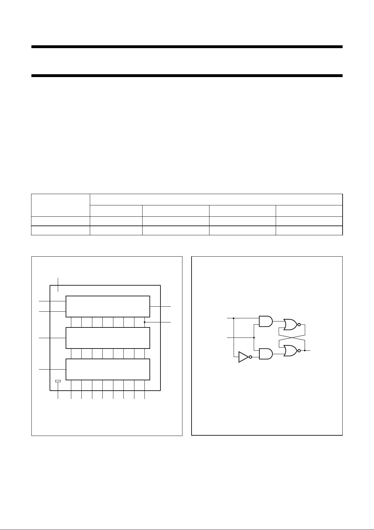
GENERAL DESCRIPTION
The HEF4794B is an 8-stage serial shift register having a
storage latch associated with each stage for strobing data
from the serial input to parallel LED driver outputs
O
to O7. Data is shifted on positive-going clock
0
transitions. The data in each shift register stage is
available at OS on positive-going clock edges to allow
high-speed operation in cascaded systems in which the
clock rise time is fast. The same serial information is
available at OS' on the next negative-going clock edge and
provides cascading HEF4794B devices when the clock
rise time is slow.
ORDERING INFORMATION
PACKAGES
TYPE NUMBER
PINS PIN POSITION MATERIAL CODE
HEF4794BT 16 SO16 plastic SOT109-1
HEF4794BP 16 DIP16 plastic SOT38-1
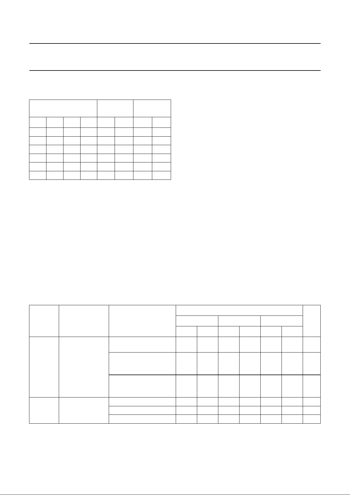
FUNCTIONAL DIAGRAM
LOGIC DIAGRAMS
CP
STR
EO
D2
3
1
15
V
DD
16
48 5 6 7 14 13 12 11
V
O0O1O2O3O4O5O6O
SS
HEF4794B
8-STAGE SHIFT
REGISTER
8-BIT STORAGE
REGISTER
OPEN-DRAIN OUTPUTS
Fig.1 Functional diagram.
O '
10
S
O
9
S
MBD909
7
handbook, halfpage
D
CP
O
MBD912
Fig.2 One D-latch.
1999 Jun 30 2
Philips Semiconductors Product specification
8-stage shift-and-store register LED driver HEF4794B
handbook, full pagewidth
STAGE 0
STAGE 1 to 6 STAGE 7
PINNING
CP
STR
EO
D
DO
CP
FF
1
DO
CP
latch
1
DO
DO
CP
FF
8
DO
CP
latch
8
DQ
CP
latch
O
O '
S
S
HEF4794B
O
O1O2O3O4O5O
0
6
O
7
MBD911
Fig.3 Logic diagram.
SYMBOL PIN DESCRIPTION
STR 1 strobe input
D 2 data input
CP 3 clock input
O
0
to O
3
4 to 7 parallel outputs 0 to 3
(open drain)
V
SS
O
' 9 and 10 serial outputs
S,OS
O
7
O
6
O
5
O
4
8 ground
11 parallel output 7 (open drain)
12 parallel output 6 (open drain)
13 parallel output 5 (open drain)
14 parallel output 4 (open drain)
EO 15 output enable input
V
DD
16 supply voltage
1999 Jun 30 3
handbook, halfpage
STR
CP
O
O
O
O
V
SS
1
D
2
3
4
0
HEF4794B
5
1
6
2
7
3
8
16
15
14
13
12
11
10
9
MBD910
Fig.4 Pin configuration.
V
DD
EO
O
O
O
O
O '
O
4
5
6
7
S
S
Philips Semiconductors Product specification
8-stage shift-and-store register LED driver HEF4794B
FUNCTIONAL DESCRIPTION
Table 1 Function table; note 1
INPUTS
CP EO STR D O
PARALLEL
OUTPUTS
O
0
↑ LXXZZO
n
SERIAL
OUTPUTS
O
OS'
S
'nc
6
↓ LXXZZncO
↑HLXncncO
↑ HHL LO
↑ HHHHO
n−1
n−1
'nc
6
O
'nc
6
O
'nc
6
↓ H H H nc nc nc O
Note
1. H = HIGH state;
L = LOW state;
X = don’t care;
↑ = positive-going transition;
↓ = negative-going transition;
Z = high-impedance OFF state;
nc = no change;
O
' = the information in the seventh shift register
6
stage.
a) At the positive clock edge the information in the
7thregister stage is transferred to the 8thregister
stage and the OSoutput.
FAMILY DATA
See
“Family Specifications”
except for: rating for DC
current into any open-drain output is 40 mA.
I
LIMITS CATEGORY MSI
DD
See
“Family Specifications”
7
7
for ratings.
DC CHARACTERISTICS
V
=0V.
SS
SYMBOL PARAMETER CONDITIONS
V
OL
LOW level output
voltage
VI=VSSor VDD;
IO < 20 mA; VDD=5V
V
I=VSS
or VDD;
IO < 20 mA;
VDD=10V
V
I=VSS
or VDD;
IO < 20 mA;
VDD=15V
I
OZH
HIGH level output
leakage current;
3-state
VO=15V; VDD=5V − 2 − 2 − 15 µA
=15V; VDD=10V − 2 − 2 − 15 µA
V
O
V
=15V; VDD=15V − 2 − 2 − 15 µA
O
1999 Jun 30 4
T
(°C)
amb
MIN. MAX. MIN. MAX. MIN. MAX.
− 0.75 − 0.75 − 1.5 V
− 0.75 − 0.75 − 1.5 V
− 0.75 − 0.75 − 1.5 V
UNIT−40 +25 +85
Philips Semiconductors Product specification
8-stage shift-and-store register LED driver HEF4794B
AC POWER CHARACTERISTICS
V
=0V; T
SS
SYMBOL PARAMETER CONDITIONS TYPICAL FORMULA FOR P (µW)
P dynamic power dissipation per
Note
1. Where:
R
= ∞;
L
fi= input frequency (MHz);
fo= output frequency (MHz);
CL= load capacitance (pF);
Σ(foCL) = sum of outputs;
VDD= supply voltage (V).
=25°C; input transition times ≤ 20 ns; unless otherwise specified.
amb
VDD=5V
package
V
=10V
DD
=15V
V
DD
1200fiΣ foCL()V
5550f
15000f
Σ foCL()V
i
Σ foCL()V
i
2
×+
DD
2
×+
DD
2
×+
DD
(1)
AC TIMING CHARACTERISTICS
V
SS
=0V; T
=25°C; CL= 50 pF; input transition times ≤20 ns; unless otherwise specified.
amb
SYMBOL PARAMETER
t
PHL
propagation delay time CP to OS;
HIGH-to-LOW
t
PLH
propagation delay time CP to OS;
LOW-to-HIGH
t
PHL
propagation delay time CP to OS';
HIGH-to-LOW
t
PLH
propagation delay time CP to OS';
LOW-to-HIGH
t
PZL
propagation delay time CP to On;
OFF-to-LOW
t
PLZ
propagation delay time CP to On;
LOW-to-OFF
V
(V)
DD
MIN. TYP. MAX. UNIT
TYPICAL
EXTRAPOLATION
FORMULA
5 − 160 320 ns 132 ns + (0.55 ns/pF)C
10 − 65 130 ns 53 ns + (0.23 ns/pF)C
15 − 45 90 ns 37 ns + (0.16 ns/pF)C
5 − 130 260 ns 102 ns + (0.55 ns/pF)C
10 − 55 110 ns 44 ns + (0.23 ns/pF)C
15 − 40 80 ns 32 ns + (0.16 ns/pF)C
5 − 120 240 ns 92 ns + (0.55 ns/pF)C
10 − 50 100 ns 39 ns + (0.23 ns/pF)C
15 − 40 80 ns 32 ns + (0.16 ns/pF)C
5 − 130 260 ns 102 ns + (0.55 ns/pF)C
10 − 60 120 ns 49 ns + (0.23 ns/pF)C
15 − 45 90 ns 37 ns + (0.16 ns/pF)C
5 − 240 480 ns note 1
10 − 80 160 ns
15 − 55 110 ns
5 − 170 340 ns note 1
10 − 75 150 ns
15 − 60 120 ns
L
L
L
L
L
L
L
L
L
L
L
L
1999 Jun 30 5
 Loading...