

Philips HEF4502BT, HEF4502BPB, HEF4502BP, HEF4502BDB, HEF4502BD Datasheet
DATA SH EET
Product specification
File under Integrated Circuits, IC04
January 1995
INTEGRATED CIRCUITS
HEF4502B
buffers
Strobed hex inverter/buffer
For a complete data sheet, please also download:
•The IC04 LOCMOS HE4000B Logic
Family Specifications HEF, HEC
•The IC04 LOCMOS HE4000B Logic
Package Outlines/Information HEF, HEC
January 1995 2
Philips Semiconductors Product specification
Strobed hex inverter/buffer
HEF4502B
buffers
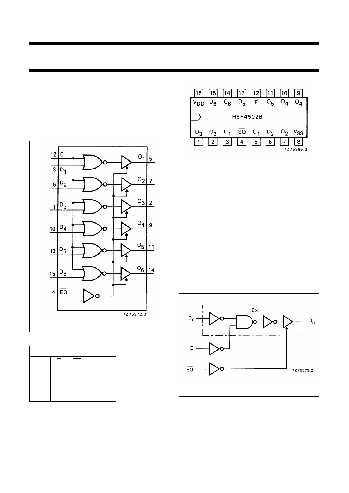
DESCRIPTION
The HEF4502B consists of six inverter/buffers with 3-state
outputs. When the output enable input (EO) is HIGH all six
outputs (O1to O6) are in the high impedance OFF-state.
When the enable input (E) is HIGH all six outputs are
switched to LOW. The outputs have a 2-TTL load drive
capability.
Fig.1 Functional diagram.
PINNING
HEF4502BP(N): 16-lead DIL; plastic (SOT38-1)
HEF4502BD(F): 16-lead DIL; ceramic (cerdip) (SOT74)
HEF4502BT(D): 16-lead SO; plastic (SOT109-1)
( ): Package Designator North America
D
1
to D
6
data inputs
E enable input
EO output enable input
O
1
to O
6
3-state outputs
Fig.2 Pinning diagram.
TRUTH TABLE
Notes
1. H = HIGH state (the more pos. voltage)
L = LOW state (the less pos. voltage)
X = state is immaterial
Z = high impedance off state
INPUTS OUTPUT
D
n
E EO O
n
LLL H
HLL L
XHL L
XXH Z
FAMILY DATA, IDDLIMITS category BUFFERS
See Family Specifications
Fig.3 Logic diagram.
 Loading...