

Philips HEF4076BU, HEF4076BT, HEF4076BPB, HEF4076BP, HEF4076BDB Datasheet
...
DATA SH EET
Product specification
File under Integrated Circuits, IC04
January 1995
INTEGRATED CIRCUITS
HEF4076B
MSI
Quadruple D-type register with
3-state outputs
For a complete data sheet, please also download:
•The IC04 LOCMOS HE4000B Logic
Family Specifications HEF, HEC
•The IC04 LOCMOS HE4000B Logic
Package Outlines/Information HEF, HEC
January 1995 2
Philips Semiconductors Product specification
Quadruple D-type register with 3-state outputs
HEF4076B
MSI
DESCRIPTION
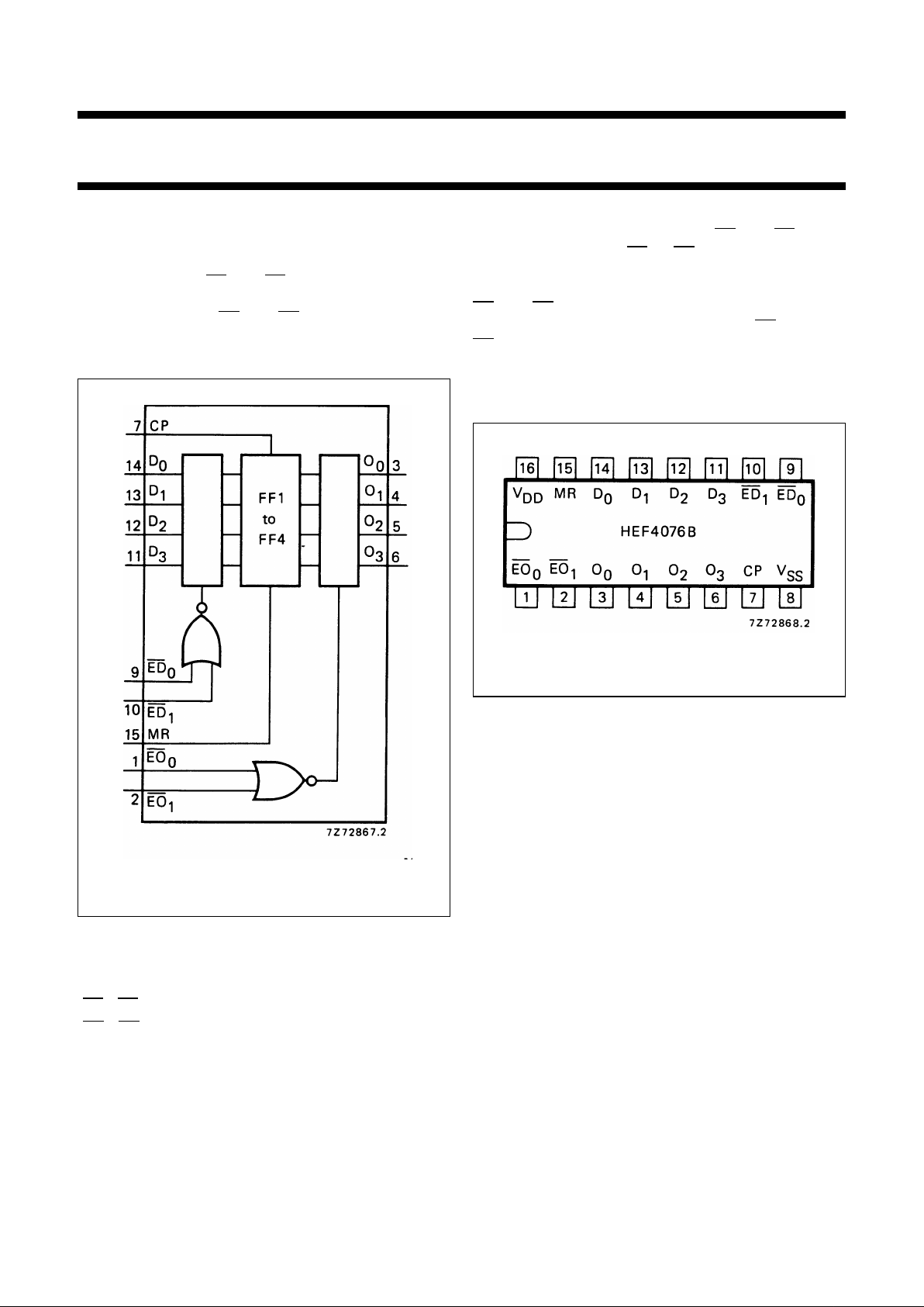
The HEF4076B is a quadruple edge-triggered D-type
flip-flop with four data inputs (D0to D3), two active LOW
data enable inputs (ED0and ED1), a common clock input
(CP), four 3-state outputs (O0to O3), two active LOW
output enable inputs (EO0and EO1), and an overriding
asynchronous master reset input (MR).
Information on D
0
to D3is stored in the four flip-flops on the
LOW to HIGH transition of CP if both ED0and ED1are
LOW. A HIGH on either ED0or ED1prevents the flip-flops
from changing on the LOW to HIGH transition of CP,
independent of the information on D0to D3. When both
EO0and EO1are LOW, the contents of the four flip-flops
are available at O0to O3. A HIGH on either EO0or
EO1forces O0to O3into the high impedance OFF-state. A
HIGH on MR resets all four flip-flops, independent of all
other input conditions.
Fig.1 Functional diagram.
HEF4076BP(N): 16-lead DIL; plastic
(SOT38-1)
HEF4076BD(F): 16-lead DIL; ceramic (cerdip)
(SOT74)
HEF4076BT(D): 16-lead SO; plastic
(SOT109-1)
( ): Package Designator North America
Fig.2 Pinning diagram.
PINNING
D
0
to D
3
data inputs
ED0, ED
1
data enable inputs (active LOW)
EO0, EO
1
output enable inputs (active LOW)
CP clock input (LOW to HIGH, edge-triggered)
MR master reset input
O
0
to O
3
data outputs
FAMILY DATA, IDDLIMITS category MSI
See Family Specifications
January 1995 3
Philips Semiconductors Product specification
Quadruple D-type register with 3-state outputs
HEF4076B
MSI
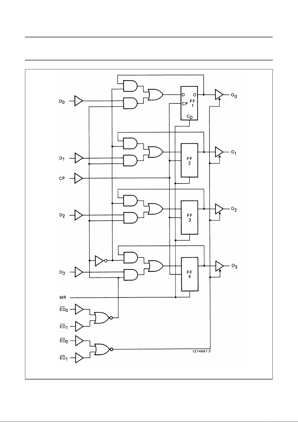
Fig.3 Logic diagram.
 Loading...