

Philips hef4066b DATASHEETS

INTEGRATED CIRCUITS
DATA SH EET
For a complete data sheet, please also download:
•The IC04 LOCMOS HE4000B Logic
Family Specifications HEF, HEC
•The IC04 LOCMOS HE4000B Logic
Package Outlines/Information HEF, HEC
HEF4066B
gates
Quadruple bilateral switches
Product specification
File under Integrated Circuits, IC04
January 1995
Philips Semiconductors Product specification
Quadruple bilateral switches
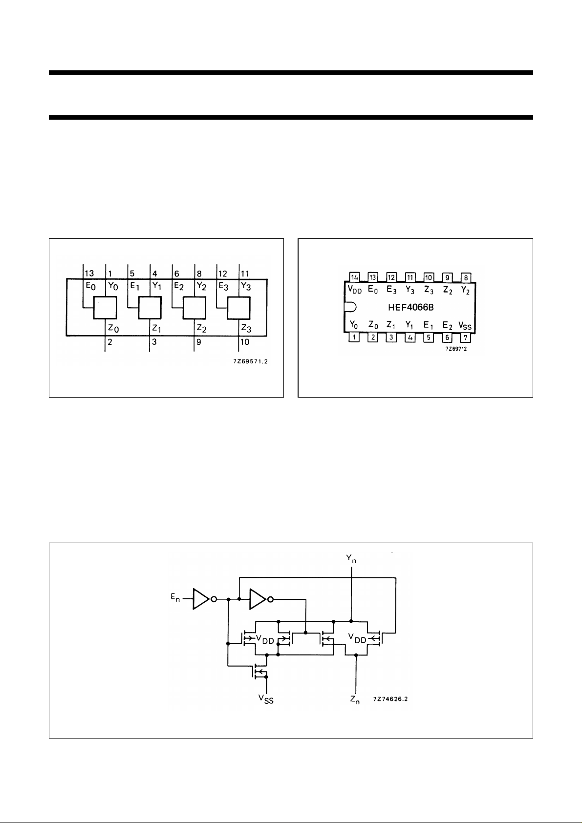
DESCRIPTION
The HEF4066B has four independent bilateral analogue
switches (transmission gates). Each switch has two
input/output terminals (Y/Z) and an active HIGH enable
input (E). When E is connected to VDDa low impedance
bidirectional path between Y and Z is established (ON
condition). When E is connected to VSSthe switch is
HEF4066B
gates
disabled and a high impedance between Y and Z is
established (OFF condition).
The HEF4066B is pin compatible with the HEF4016B but
exhibits a much lower ON resistance. In addition the ON
resistance is relatively constant over the full input signal
range.
Fig.1 Functional diagram. Fig.2 Pinning diagram.
HEF4066BP(N): 14-lead DIL; plastic (SOT27-1)
HEF4066BD(F): 14-lead DIL; ceramic (cerdip)
(SOT73))
HEF4066BT(D): 14-lead SO; plastic (SOT108-1)
( ): Package Designator North America
PINNING
to E
E
0
Y
to Y
0
to Z
Z
0
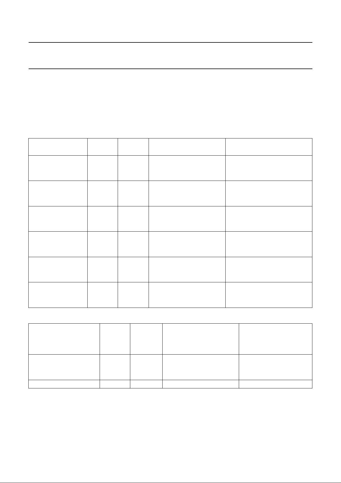
APPLICATION INFORMATION
An example of application for the HEF4066B is:
• Analogue and digital switching
enable inputs
3
input/output terminals
3
input/output terminals
3
Fig.3 Schematic diagram (one switch).
January 1995 2
Philips Semiconductors Product specification
Quadruple bilateral switches
HEF4066B
RATINGS
Limiting values in accordance with the Absolute Maximum System (IEC 134)
Power dissipation per switch P max. 100 mW
For other RATINGS see Family Specifications
DC CHARACTERISTICS
=25°C
T
amb
V
DD
V
5
ON resistance
10 − 80 245 Ω Vis=VSSto V
15 − 60 175 Ω see Fig.4
5
ON resistance
10 − 50 160 Ω Vis=V
15 − 40 115 Ω see Fig.4
5
ON resistance
10 − 65 200 Ω Vis=V
15 − 50 155 Ω see Fig.4
‘∆’ ON resistance 5
between any two 10 − 10 −Ω Vis=VSSto V
channels 15 − 5 −Ω see Fig.4
OFF state leakage 5
current, any 10 −−−nA
channel OFF 15 −−200 nA
E
input voltage 5
n
LOW 10 − 4,50 2 V
15 − 6,75 2 V
SYMBOL MIN. TYP. MAX. CONDITIONS
R
R
R
∆R
− 350 2500 Ω Enat V
ON
− 115 340 Ω Enat V
ON
− 120 365 Ω Enat V
ON
− 25 −Ω Enat V
ON
DD
DD
DD
SS
DD
DD
DD
DD
−−−nA
I
OZ
E
at V
n
SS
− 2,25 1 V
=10µA
I
V
IL
is
see Fig.9
gates
V
DD
V
SYMBOL T
−40 +25 +85
(°c) CONDITIONS
amb
MAX. MAX. MAX.
Quiescent device 5
current 10 2,0 2,0 15,0 µA input combinations;
I
DD
15 4,0 4,0 30,0 µAV
Input leakage current at E
n
15 ± I
IN
1,0 1,0 7,5 µAV
= 0; all valid
SS
I=VSS
or V
− 300 1000 nA Enat VSSor V
January 1995 3
DD
DD
 Loading...