

Philips HEF4051BU, HEF4051BT, HEF4051BPB, HEF4051BP, HEF4051BDB Datasheet
...
DATA SH EET
Product specification
File under Integrated Circuits, IC04
January 1995
INTEGRATED CIRCUITS
HEF4051B
MSI
8-channel analogue
multiplexer/demultiplexer
For a complete data sheet, please also download:
•The IC04 LOCMOS HE4000B Logic
Family Specifications HEF, HEC
•The IC04 LOCMOS HE4000B Logic
Package Outlines/Information HEF, HEC
January 1995 2
Philips Semiconductors Product specification
8-channel analogue multiplexer/demultiplexer
HEF4051B
MSI
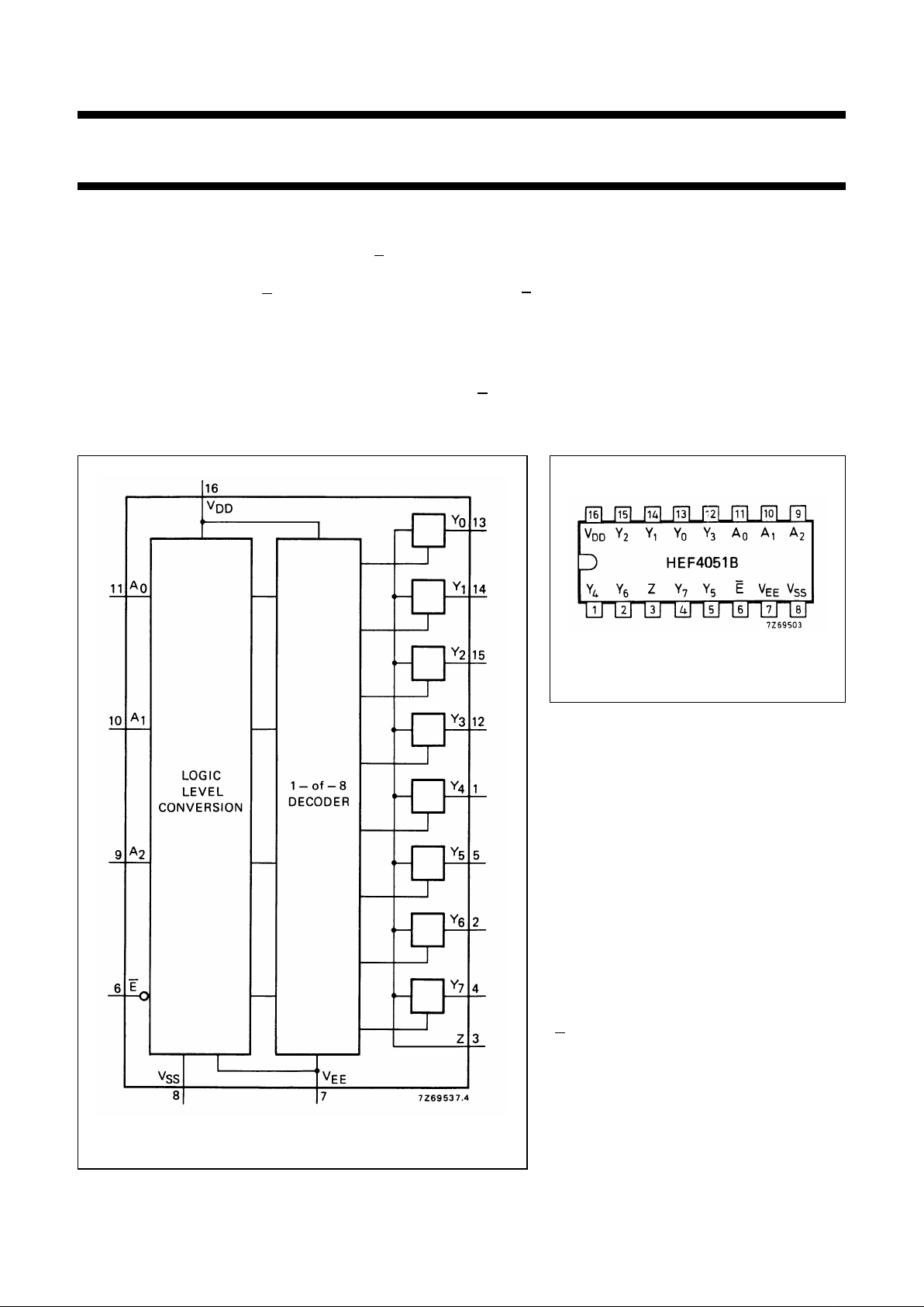
DESCRIPTION
The HEF4051B is an 8-channel
analogue multiplexer/demultiplexer
with three address inputs (A0to A2),
an active LOW enable input (E), eight
independent inputs/outputs (Y0to Y7)
and a common input/output (Z).
The device contains eight
bidirectional analogue switches, each
with one side connected to an
independent input/output (Y
0
to Y7)
and the other side connected to a
common input/output (Z).
With
E LOW, one of the eight
switches is selected (low impedance
ON-state) by A0to A2. With E HIGH,
all switches are in the high impedance
OFF-state, independent of A0to A2.
VDDand VSSare the supply voltage
connections for the digital control
inputs (A0to A2, and E).
The VDDto VSSrange is 3 to 15 V.
The analogue inputs/outputs (Y0to
Y7, and Z) can swing between VDDas
a positive limit and VEEas a negative
limit. VDD−VEEmay not exceed 15 V.
For operation as a digital
multiplexer/demultiplexer, VEEis
connected to VSS(typically ground).
Fig.1 Functional diagram.
PINNING
FAMILY DATA, I
DD
LIMITS category MSI
See Family Specifications.
HEF4051BP(N): 16-lead DIL; plastic
(SOT38-1)
HEF4051BD(F): 16-lead DIL; ceramic
(cerdip)
(SOT74)
HEF4051BT(D): 16-lead SO; plastic
(SOT109-1)
( ): Package Designator North America
Y
0
to Y
7
independent inputs/outputs
A
0
to A
2
address inputs
E enable input (active LOW)
Z common input/output
Fig.2 Pinning diagram.
January 1995 3
Philips Semiconductors Product specification
8-channel analogue multiplexer/demultiplexer
HEF4051B
MSI
FUNCTION TABLE
Notes
1. H = HIGH state (the more positive voltage)
L = LOW state (the less positive voltage)
X = state is immaterial
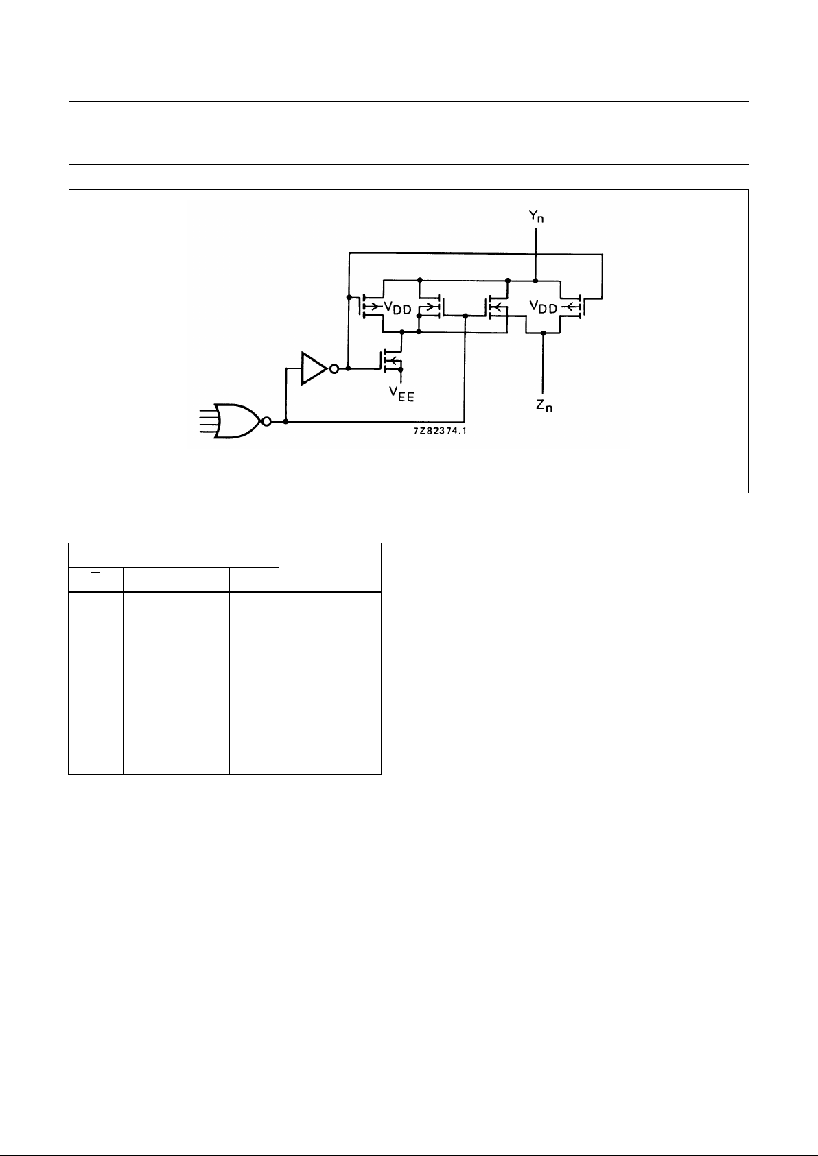
RATINGS
Limiting values in accordance with the Absolute Maximum System (IEC 134)
Note
1. To avoid drawing V
DD
current out of terminal Z, when switch current flows into terminals Y, the voltage drop across
the bidirectional switch must not exceed 0,4 V. If the switch current flows into terminal Z, no VDDcurrent will flow out
of terminals Y, in this case there is no limit for the voltage drop across the switch, but the voltages at Y and Z may
not exceed VDDor VEE.
INPUTS CHANNEL
ON
EA
2
A
1
A
0
LLLL Y
0
−Z
LLLH Y
1
−Z
LLHL Y
2
−Z
LLHH Y
3
−Z
LHLL Y
4
−Z
LHLH Y
5
−Z
LHHL Y
6
−Z
LHHH Y
7
−Z
H X X X none
Supply voltage (with reference to V
DD
)V
EE
−18 to + 0,5 V
Fig.3 Schematic diagram (one switch).
 Loading...