

Philips HEF4047BT, HEF4047BPB, HEF4047BP, HEF4047BDB, HEF4047BD Datasheet

DATA SH EET
Product specification
File under Integrated Circuits, IC04
January 1995
INTEGRATED CIRCUITS
HEF4047B
MSI
Monostable/astable multivibrator
For a complete data sheet, please also download:
•The IC04 LOCMOS HE4000B Logic
Family Specifications HEF, HEC
•The IC04 LOCMOS HE4000B Logic
Package Outlines/Information HEF, HEC
January 1995 2
Philips Semiconductors Product specification
Monostable/astable multivibrator
HEF4047B
MSI
DESCRIPTION
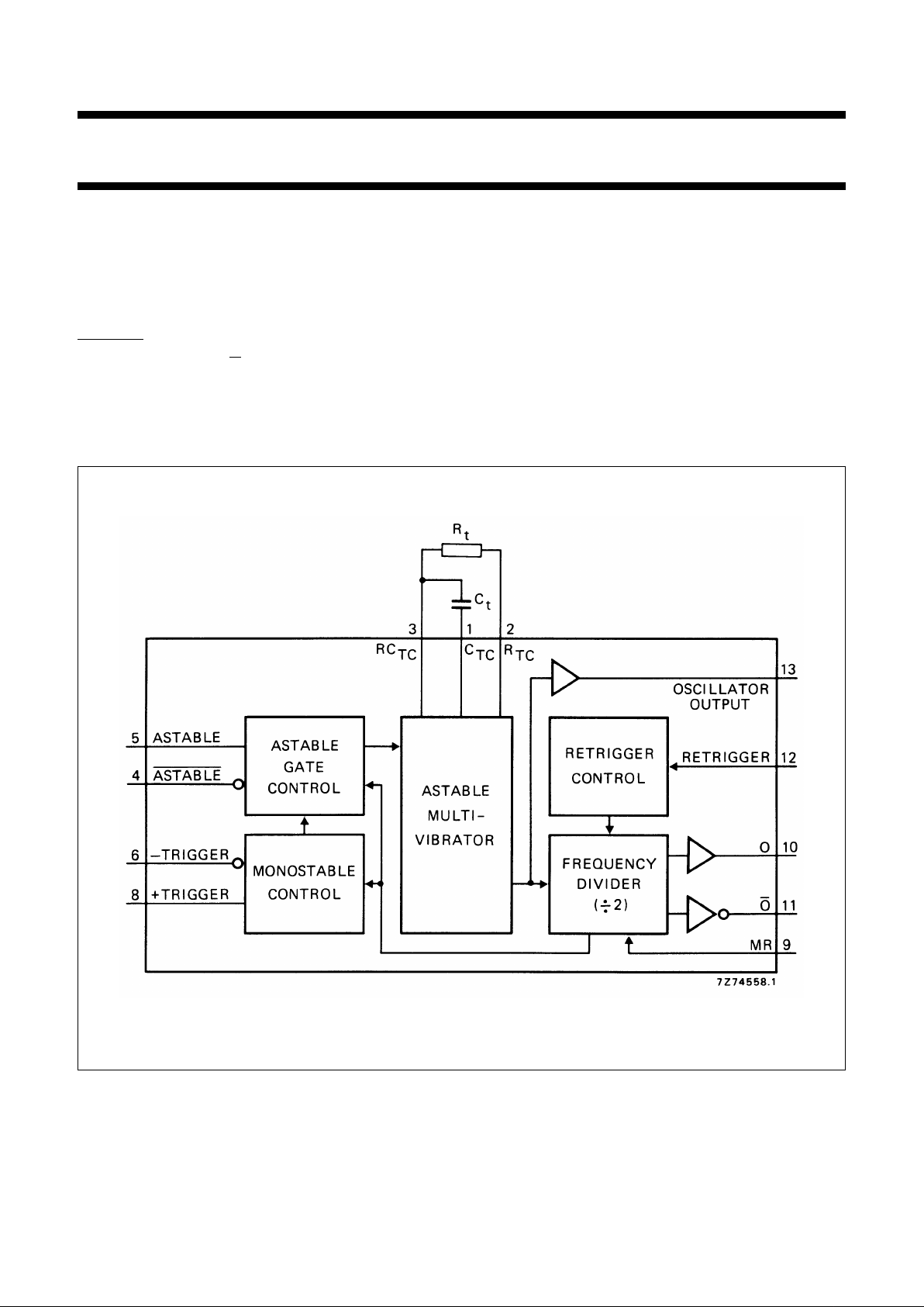
The HEF4047B consists of a gatable astable multivibrator
with logic techniques incorporated to permit positive or
negative edge-triggered monostable multivibrator action
with retriggering and external counting options.
Inputs include + TRIGGER, − TRIGGER, ASTABLE,
ASTABLE, RETRIGGER and MR (Master Reset).
Buffered outputs are O,O and OSCILLATOR OUTPUT. In
all modes of operation an external capacitor (Ct) must be
connected between CTCand RCTC, and an external
resistor (R
t
) must be connected between RTCand
RCTC(continued on next page).
FAMILY DATA, I
DD
LIMITS category MSI
See Family Specifications
Fig.1 Functional diagram.
January 1995 3
Philips Semiconductors Product specification
Monostable/astable multivibrator
HEF4047B
MSI
Astable operation is enabled by a HIGH level on the
ASTABLE input. The period of the square wave at O and
O outputs is a function of the external components
employed. ‘True’ input pulses on the ASTABLE or
‘complement’ pulses on the ASTABLE input, allow the
circuit to be used as a gatable multivibrator. The
OSCILLATOR OUTPUT period will be half of the O output
in the astable mode. However, a 50% duty factor is not
guaranteed at this output.
In the monostable mode, positive edge-triggering is
accomplished by applying a leading-edge pulse to the
+ TRIGGER input and a LOW level to the − TRIGGER
input. For negative edge-triggering, a trailing-edge pulse is
applied to the − TRIGGER and a HIGH level to the
+ TRIGGER. Input pulses may be of any duration relative
to the output pulse. The multivibrator can be retriggered
(on the leading-edge only) by applying a common pulse to
both the RETRIGGER and + TRIGGER inputs. In this
mode the output pulse remains HIGH as long as the input
pulse period is shorter than the period determined by the
RC components.
An external count down option can be implemented by
coupling O to an external ‘N’ counter and resetting the
counter with the trigger pulse. The counter output pulse is
fed back to the ASTABLE input and has a duration equal
to N times the period of the multivibrator. A HIGH level on
the MR input assures no output pulse during an ON-power
condition. This input can also be activated to terminate the
output pulse at any time. In the monostable mode, a HIGH
level or power-ON reset pulse must be applied to MR,
whenever VDDis applied.
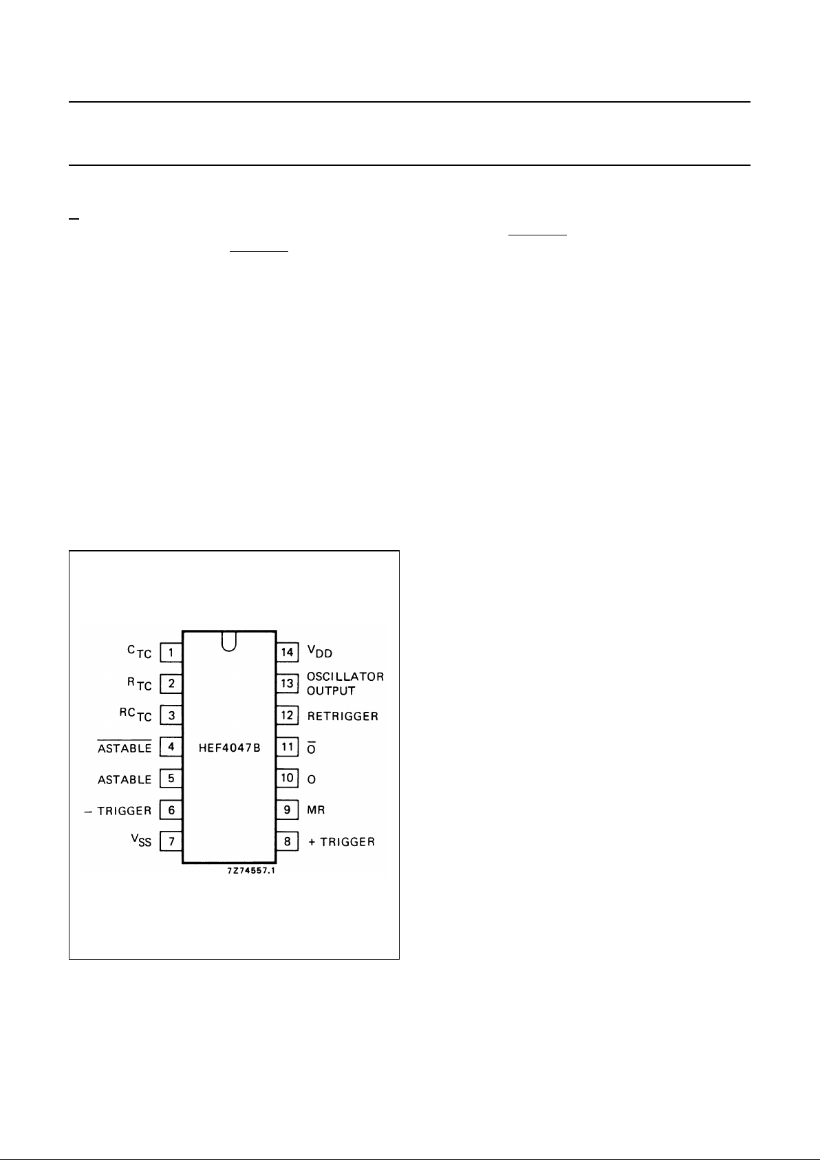
Fig.2 Pinning diagram.
HEF4047BP(N): 14-lead DIL; plastic
(SOT27-1)
HEF4047BD(F): 14-lead DIL; ceramic (cerdip)
(SOT73)
HEF4047BT(D): 14-lead SO; plastic
(SOT108-1)
( ): Package Designator North America
January 1995 4
Philips Semiconductors Product specification
Monostable/astable multivibrator
HEF4047B
MSI
This text is here in white to force landscape pages to be rotated correctly when browsing through the pdf in the Acrobat reader.This text is here in
_white to force landscape pages to be rotated correctly when browsing through the pdf in the Acrobat reader.This text is here inThis text is here in
white to force landscape pages to be rotated correctly when browsing through the pdf in the Acrobat reader. white to force landscape pages to be ...
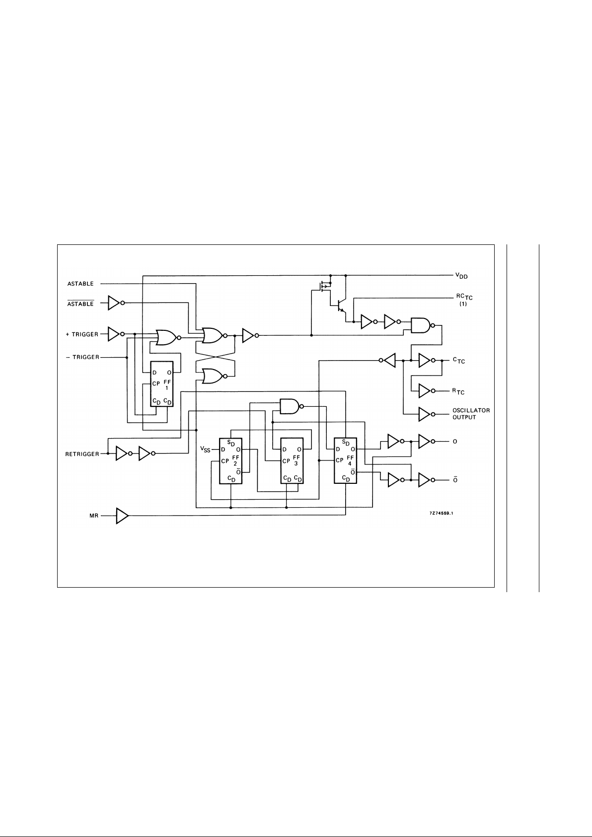
Fig.3 Logic diagram.
(1) Special input protection that allows operating input voltages
outside the supply voltage lines. Compared to the standard input
protection pin 3 is more sensitive to static discharge; extra
handling precautions are recommended.

January 1995 5
Philips Semiconductors Product specification
Monostable/astable multivibrator
HEF4047B
MSI
FUNCTIONAL CONNECTIONS
Notes
1. Input pulse to RESET of external counting chip; external counting chip output to pin 4.
2. In all cases, external resistor between pins 2 and 3, external capacitor between pins 1 and 3.
DC CHARACTERISTICS
V
SS
= 0 V; inputs at VSSor V
DD
FUNCTION
PINS CONNECTED TO OUTPUT
PULSE
FROM
PINS
OUTPUT
PERIOD
OR
PULSE WIDTH
V
DD
V
SS
INPUT
PULSE
astable multivibrator
free running 4, 5, 6, 14 7, 8, 9, 12 − 10, 11, 13 at pins 10, 11:
true gating 4, 6, 14 7, 8, 9, 12 5 10, 11, 13 t
A
= 4,40 RtC
t
at pin 13:
tA= 2,20 RtC
t
complement gating 6, 14 5, 7, 8, 9, 12 4 10, 11, 13
monostable multivibrator
pos. edge-triggering 4, 14 5, 6, 7, 9, 12 8 10, 11
neg. edge-triggering 4, 8, 14 5, 7, 9, 12 6 10, 11 at pins 10, 11:
retriggerable 4, 14 5, 6, 7, 9 8, 12 10, 11 t
M
= 2,48 RtC
t
external count down
(1)
14 5, 6, 7, 8, 9, 12 − 10, 11
V
DD
V
SYMBOL
T
amb
(°C)
−40 + 25 + 85
MAX. MIN. MAX. MAX.
Leakage current
15 I
3
0,3 − 0,3 1 µA
pin 3 at
VDDor V
SS
pin 3; output
transistor OFF
 Loading...