

Philips HEF4046BD, HEF4046BU, HEF4046BT, HEF4046BPB, HEF4046BP Datasheet
...
DATA SH EET
Product specification
File under Integrated Circuits, IC04
January 1995
INTEGRATED CIRCUITS
HEF4046B
MSI
Phase-locked loop
For a complete data sheet, please also download:
•The IC04 LOCMOS HE4000B Logic
Family Specifications HEF, HEC
•The IC04 LOCMOS HE4000B Logic
Package Outlines/Information HEF, HEC
January 1995 2
Philips Semiconductors Product specification
Phase-locked loop
HEF4046B
MSI
DESCRIPTION
The HEF4046B is a phase-locked loop circuit that consists
of a linear voltage controlled oscillator (VCO) and two
different phase comparators with a common signal input
amplifier and a common comparator input. A 7 V regulator
(zener) diode is provided for supply voltage regulation if
necessary. For functional description see further on in this
data.
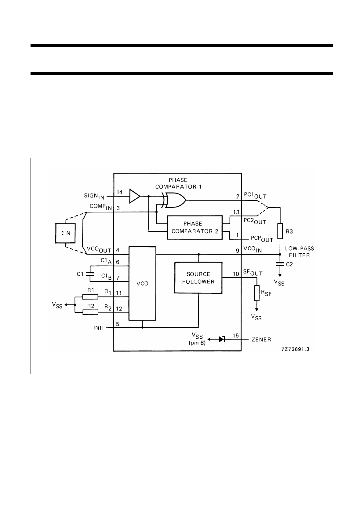
Fig.1 Functional diagram.
HEF4046BP(N): 16-lead DIL; plastic
(SOT38-1)
HEF4046BD(F): 16-lead DIL; ceramic (cerdip)
(SOT74)
HEF4046BT(D): 16-lead SO; plastic
(SOT109-1)
( ): Package Designator North America
FAMILY DATA
See Family Specifications
I
DD
LIMITS category MSI
See further on in this data.
January 1995 3
Philips Semiconductors Product specification
Phase-locked loop
HEF4046B
MSI
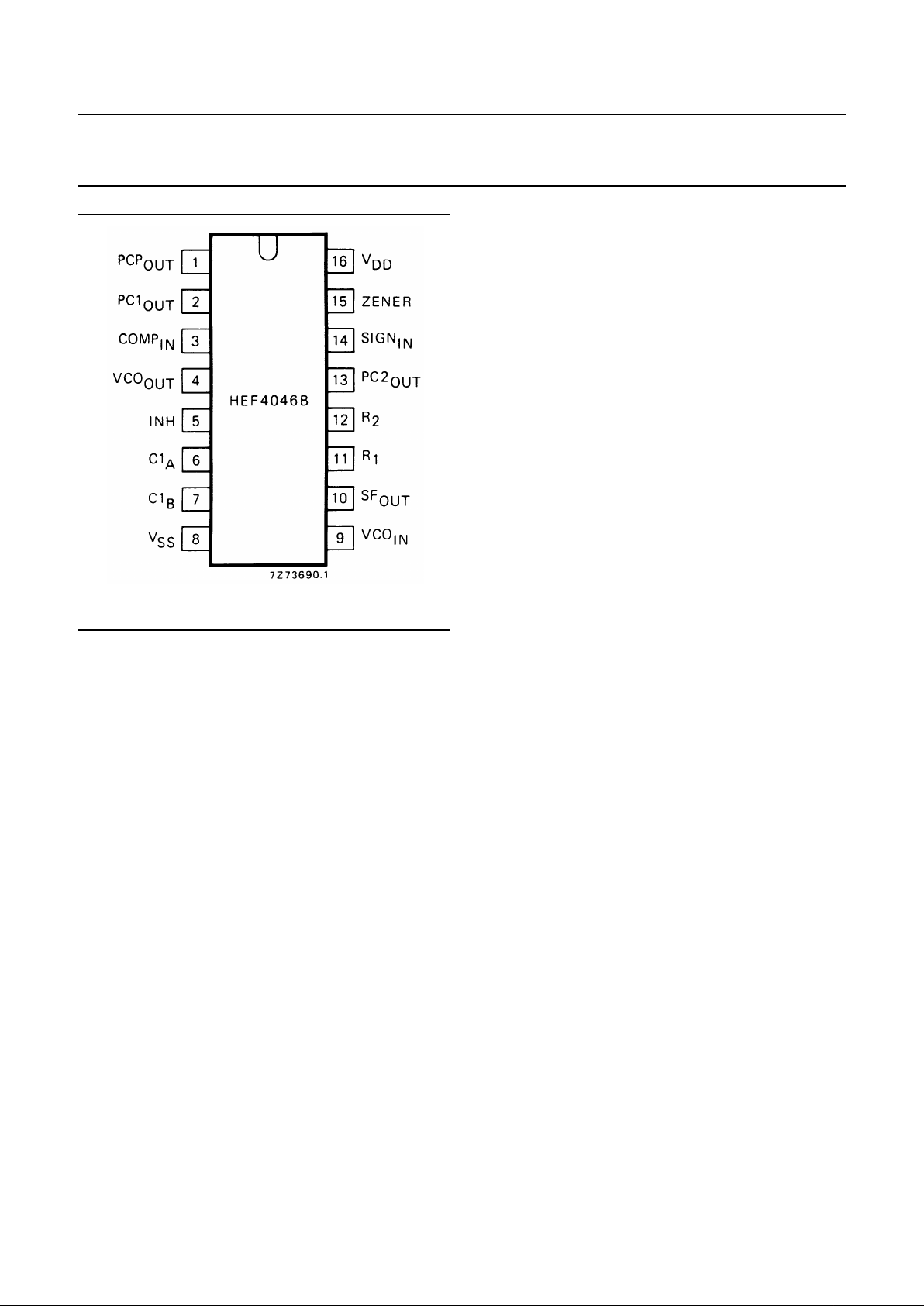
Fig.2 Pinning diagram.
PINNING
1. Phase comparator pulse output
2. Phase comparator 1 output
3. Comparator input
4. VCO output
5. Inhibit input
6. Capacitor C1 connection A
7. Capacitor C1 connection B
8. V
SS
9. VCO input
10. Source-follower output
11. Resistor R1 connection
12. Resistor R2 connection
13. Phase comparator 2 output
14. Signal input
15. Zener diode input for regulated supply.
FUNCTIONAL DESCRIPTION
VCO part
The VCO requires one external capacitor (C1) and one or
two external resistors (R1 or R1 and R2). Resistor R1 and
capacitor C1 determine the frequency range of the VCO.
Resistor R2 enables the VCO to have a frequency off-set
if required. The high input impedance of the VCO simplifies
the design of low-pass filters; it permits the designer a wide
choice of resistor/capacitor ranges. In order not to load the
low-pass filter, a source-follower output of the VCO input
voltage is provided at pin 10. If this pin (SF
OUT
) is used, a
load resistor (RSF) should be connected from this pin to
VSS; if unused, this pin should be left open. The VCO
output (pin 4) can either be connected directly to the
comparator input (pin 3) or via a frequency divider. A LOW
level at the inhibit input (pin 5) enables the VCO and the
source follower, while a HIGH level turns off both to
minimize stand-by power consumption.
Phase comparators
The phase-comparator signal input (pin 14) can be
direct-coupled, provided the signal swing is between the
standard HE4000B family input logic levels. The signal
must be capacitively coupled to the self-biasing amplifier
at the signal input in case of smaller swings. Phase
comparator 1 is an EXCLUSIVE-OR network. The signal
and comparator input frequencies must have a 50% duty
factor to obtain the maximum lock range. The average
output voltage of the phase comparator is equal to
1
⁄2V
DD
when there is no signal or noise at the signal input. The
average voltage to the VCO input is supplied by the
low-pass filter connected to the output of phase
comparator 1. This also causes the VCO to oscillate at the
centre frequency (fo). The frequency capture range (2 fc) is
defined as the frequency range of input signals on which
the PLL will lock if it was initially out of lock. The frequency
lock range (2 fL) is defined as the frequency range of input
signals on which the loop will stay locked if it was initially
in lock. The capture range is smaller or equal to the lock
range.
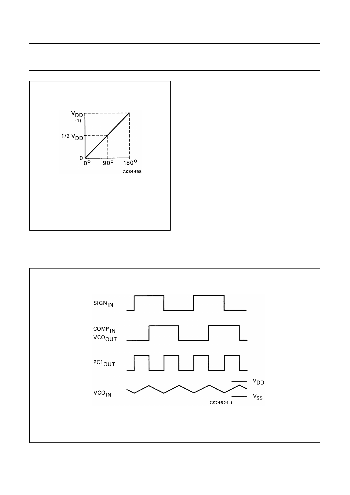
With phase comparator 1, the range of frequencies over
which the PLL can acquire lock (capture range) depends
on the low-pass filter characteristics and this range can be
made as large as the lock range. Phase comparator 1
enables the PLL system to remain in lock in spite of high
amounts of noise in the input signal. A typical behaviour of
this type of phase comparator is that it may lock onto input
frequencies that are close to harmonics of the VCO centre
frequency. Another typical behaviour is, that the phase
angle between the signal and comparator input varies
between 0° and 180° and is 90° at the centre frequency.
Figure 3 shows the typical phase-to-output response
characteristic.
January 1995 4
Philips Semiconductors Product specification
Phase-locked loop
HEF4046B
MSI
Figure 4 shows the typical waveforms for a PLL employing
phase comparator 1 in locked condition of fo.
Fig.3 Signal-to-comparator inputs phase
difference for comparator 1.
(1) Average output voltage.
Fig.4 Typical waveforms for phase-locked loop employing phase comparator 1 in locked condition of fo.
January 1995 5
Philips Semiconductors Product specification
Phase-locked loop
HEF4046B
MSI
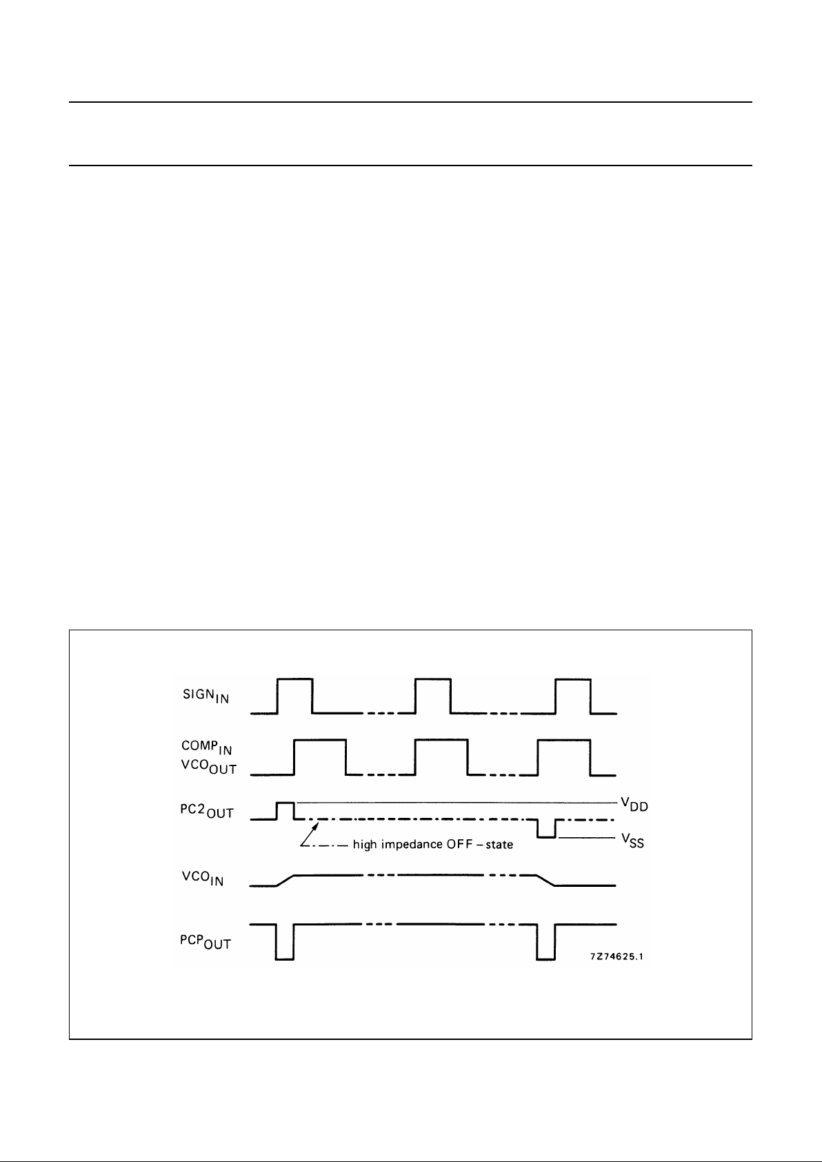
Phase comparator 2 is an edge-controlled digital memory
network. It consists of four flip-flops, control gating and a
3-state output circuit comprising p and n-type drivers
having a common output node. When the p-type or n-type
drivers are ON, they pull the output up to VDDor down to
VSSrespectively. This type of phase comparator only acts
on the positive-going edges of the signals at SIGNINand
COMPIN. Therefore, the duty factors of these signals are
not of importance.
If the signal input frequency is higher than the comparator
input frequency, the p-type output driver is maintained ON
most of the time, and both the n and p-type drivers are
OFF (3-state) the remainder of the time. If the signal input
frequency is lower than the comparator input frequency,
the n-type output driver is maintained ON most of the time,
and both the n and p-type drivers are OFF the remainder
of the time. If the signal input and comparator input
frequencies are equal, but the signal input lags the
comparator input in phase, the n-type output driver is
maintained ON for a time corresponding to the phase
difference. If the comparator input lags the signal input in
phase, the p-type output driver is maintained ON for a time
corresponding to the phase difference. Subsequently, the
voltage at the capacitor of the low-pass filter connected to
this phase comparator is adjusted until the signal and
comparator inputs are equal in both phase and frequency.
At this stable point, both p and n-type drivers remain OFF
and thus the phase comparator output becomes an open
circuit and keeps the voltage at the capacitor of the
low-pass filter constant.
Moreover, the signal at the phase comparator pulse output
(PCP
OUT
) is a HIGH level which can be used for indicating
a locked condition. Thus, for phase comparator 2 no phase
difference exists between the signal and comparator
inputs over the full VCO frequency range. Moreover, the
power dissipation due to the low-pass filter is reduced
when this type of phase comparator is used because both
p and n-type output drivers are OFF for most of the signal
input cycle. It should be noted that the PLL lock range for
this type of phase comparator is equal to the capture
range, independent of the low-pass filter. With no signal
present at the signal input, the VCO is adjusted to its
lowest frequency for phase comparator 2 . Figure 5 shows
typical waveforms for a PLL employing this type of phase
comparator in locked condition.
Fig.5 Typical waveforms for phase-locked loop employing phase comparator 2 in locked condition.
 Loading...