

Page 1

Micro Audio Jukebox HDD084/HDD085/HDD082/HDD086
A
All Versions
Service Manual
©Copyright 2005 Philips Consumer Electronics B.V. Eindhoven, The Netherlands
ll rights reserved. No part of this publication may by reproduced, stored in a
retrieval system or transmitted, in any form or by any means, electronics,
mechanical, photocopying, or otherwise without the prior permission of Philips
TABLE OF CONTENTS
Chapter
Technical Specification and Service hints.…………………1
Safety Instructions………………………………………………2
Instructions for Use……………………………………………. 3
Mechanical Instructions………………………………………. 4
Exploded view and Service parts list…………………...….. 5
Factory Service Mode testing………………………………… 6
Overall Block diagram…………………………………………. 7
Overall Electrical diagram……………………………………. 8
Component layout……………………………………………… 9
Revision list………………………………………………………10
3141 785 30487
Version 1.7
Page 2
1.0 TECHNICAL SPECIFICATION and SERVICE HINTS
General
Dimensions (WxLx H) : 53 x 86 x 16.7 mm (2.1 x 3.4 x
Weight : 78 g (2.8 oz)
Output power : 2 x 5 mW
Frequency response : 20-20 000 Hz
Equalizer : 5 band DSP controlled
Hard disk : 1,0” micro HDD
Capacity : 3GB
Display : Black/White
Backlight : White Led
Battery : 640 mAh Li-ion internal
Battery life time: >9hr
File transfer rate using
USB :
Battery charging current 320 -420mA
Maximum charging time : 4hrs
0.7 inches)
(16 ohm)
: 96 x 64 pixels
rechargeable battery
800kbyte/s
Battery cutoff voltage: 3.4V
Connections: Stereo headphone
Mini USB (B-type)
DC charger input
Battery level detection
Detection Level Typ.
4-step to 3-step voltage 3.95V
3-step to 2-step voltage 3,8V
2-step to 1-step voltage 3,7V
Force Power Off voltage 3,4V
Current consumption
DC-IN SUPPLY (3.8V)
Battery Charging Current 370mA typ.
BATT. SUPPLY (3.4V)
Power Off <15uA
Idle with LCD Backlight on 55mA
Playback without HDD reading 45mA
Playback with HDD reading 350mA
File transfer using USB1.1 350mA
Headphone out (headphone output load 2x16 ohm)
Maximum output power : 1mW
Frequency response : 20Hz - 20kHz
SNR (A-wght) :
THD (1kHz) : 0,5% - 1.0%
Left-Right Channel
Separation :
Left-Right Channel
Balance :
>75 dB
40dB typ.
0,5dB
Supported playback format
MP3 :
8 - 320 Kbps and VBR
WMA : 32 - 192 Kbps
Sample rates : 8, 11.025, 16, 22.050
32, 44.1, 48
ID3-tag support : Yes
PC Connectivity : USB
File Transfer
For HDD084
via Windows Media Player 9 or 10 for music playback
or Windows Explorer for general data (music playback
disabled)
For HDD082/HDD085/HDD086
via Windows Media Player 10 for music playback or
Windows Explorer for general data (music playback
disabled)
Firmware and software upgrades
For HDD084
1. Download the latest version of the Device
Manager application from
http://www.philips.com/support. You may need to
enter your language preference and the model
number e.g.hdd084, to access the Device
Manager application upgrade file.
2. Double click the downloaded execution file to start
the installation of the Device Manager.
3. Once the installation is completed, connect the
GoGear to the power supply with the AC/DC
adapter.
4. Launch the Device Manager at Start->Programs-
>Philips GoGear HDD->Philips GoGear HDD on
your PC
5. A dialogue box will pop up; click Upgrade to start
the upgrading of the firmware. (Please do not
disconnect the jukebox during the upgrading
process as this interruption may damage the
firmware!)
6. Follow all screen instructions to complete the
firmware upgrade.
7. The Device Manag er will close automatically once
the success message is displayed. Close all
opened application and then safely remove your
GoGear micro jukebox by clicking on the
in your task tray bar. When prompted, “The USB
Mass Storage Device can now be safely removed
from the system”, click OK and unplug your micro
jukebox.
icon
Page 3
1.0 TECHNICAL SPECIFICATION and SERVICE HINTS
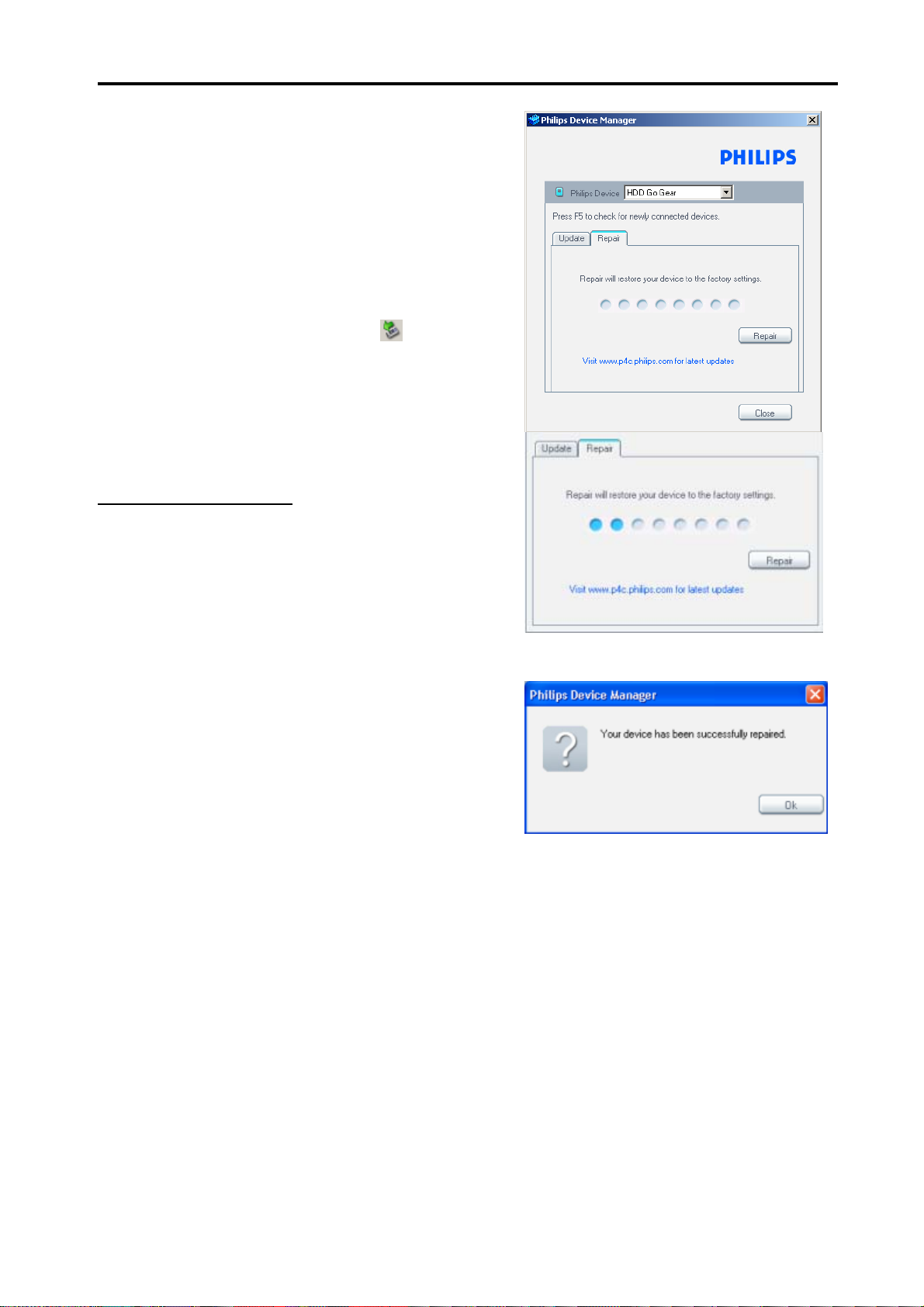
8. Once the GoGear micro jukebox is disc onnected
from the computer, the display will show “Firmware
Upgrading” for a couple of seconds and then start
up as usual. If the message does not disappear
after 2 minutes, do a soft reset by pressing and
holding the key and the volume + key for a
couple of seconds.
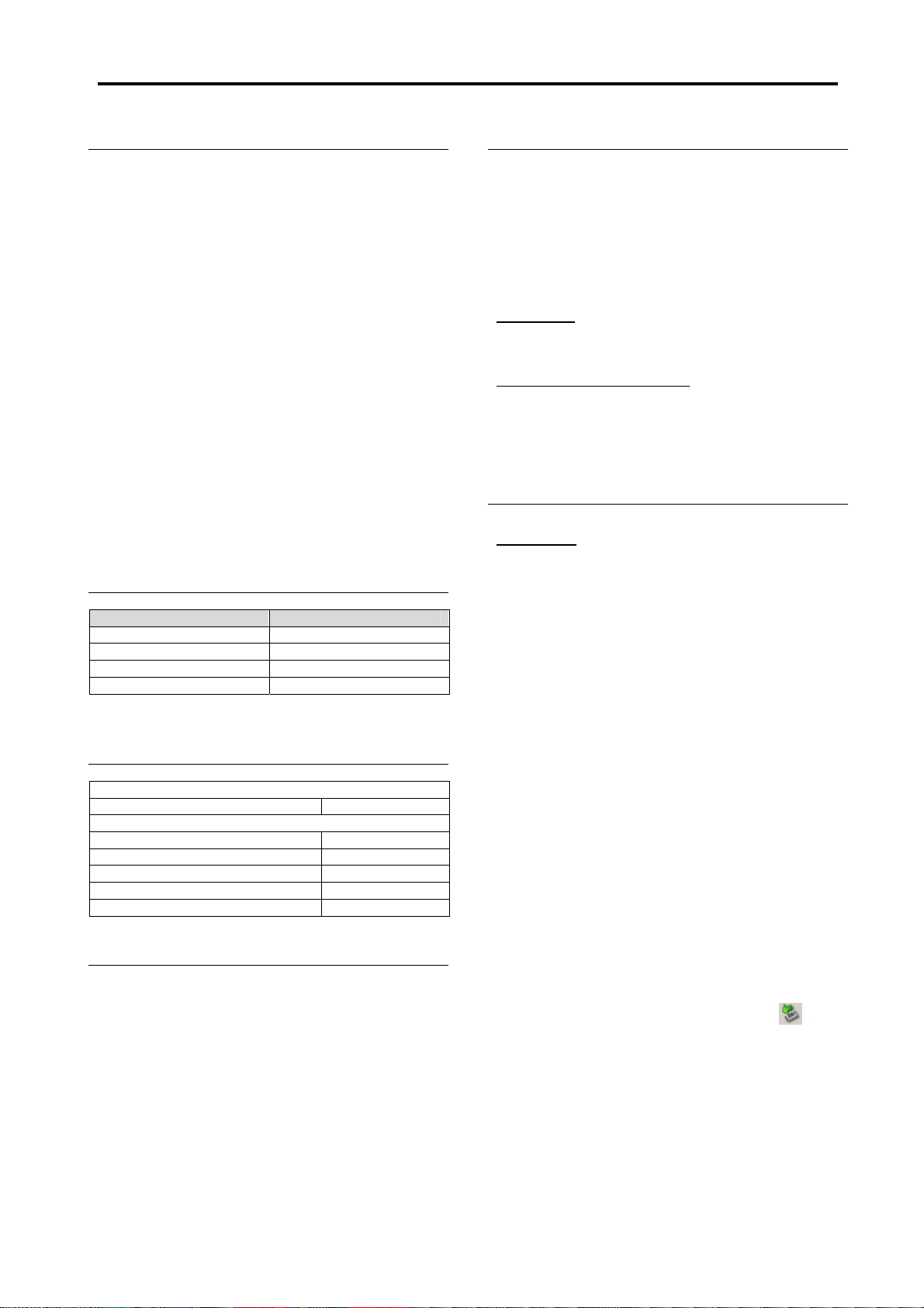
For HDD085/HDD082
1. Download the latest version of the Device
Manager application from
http://www.philips.com/support. You may need to
enter your language preference and the model
number e.g. hdd085, to access the Device
Manager application upgrade file.
2. Double click the downloaded execution file to start
the installation of the Device Manager.
3. Connect the GoGear to the power supply with the
AC/DC adapter and to the computer with the
provided USB cable. Make sure that Windows
Media Player along with any other applications are
closed.
4. Launch the Philips Device Manager by double
clicking the Device Manager icon at the task bar
on your computer.
5. The Philips Device Manager will detect the
connection of your GoGear and the application will
automatically check on the server to see if an
update is available and prompt user to download
the updated firmware. Click YES to start the
downloading.
7. The application will show the status of updating
and at the end you need to click OK to complete
the update. (Please do not disconnect the jukebox
during the upgrading process as this interruption
may damage the firmware!)
6. A status bar will show the downloading pro gress of
the firmware. Once the downloading is complete
the application will prompt you to install the update
onto your GoGear. Click YES to confirm
8. Once the success message is displayed. Close
Device Manager and all opened application and
unplug your GoGear.
Service Hints
Rebuild database & firmware after
replacement of hard disk drive
IMPORTANT: All devices having the hard disk
replaced must have the firmware image & database
rebuilt before returning to customers.
After the replacement of hard disk the database and
firmware image must be rebuilt in the device with
device manager by following the procedure below.
For HDD084
1. Connect the GoGear to the po wer supply with the
Page 4
1.0 TECHNICAL SPECIFICATION and SERVICE HINTS
AC/DC adapter and to the computer with the
provided USB cable.
2. Launch the Device Manager at Start->Programs-
>Philips GoGear HDD->Philips GoGear HDD on
your PC
A dialogue box will pop up; click Restore and OK
to confirm and start restoring the unit to its factory
setting.
3. Follow all screen instructions to complete the
restoration.
4. The Device Manag er will close automatically once
the success message is displayed. Close all
opened application and then safely remove your
GoGear micro jukebox by clicking on the
in your task tray bar. When prompted, “The USB
Mass Storage Device can now be safely removed
from the system”, click OK and unplug your micro
jukebox.
5. Once the GoGear micro jukebox is disc onnected
from the computer, the display will show “Firmware
Upgrading” for a couple of seconds and then start
up as usual.
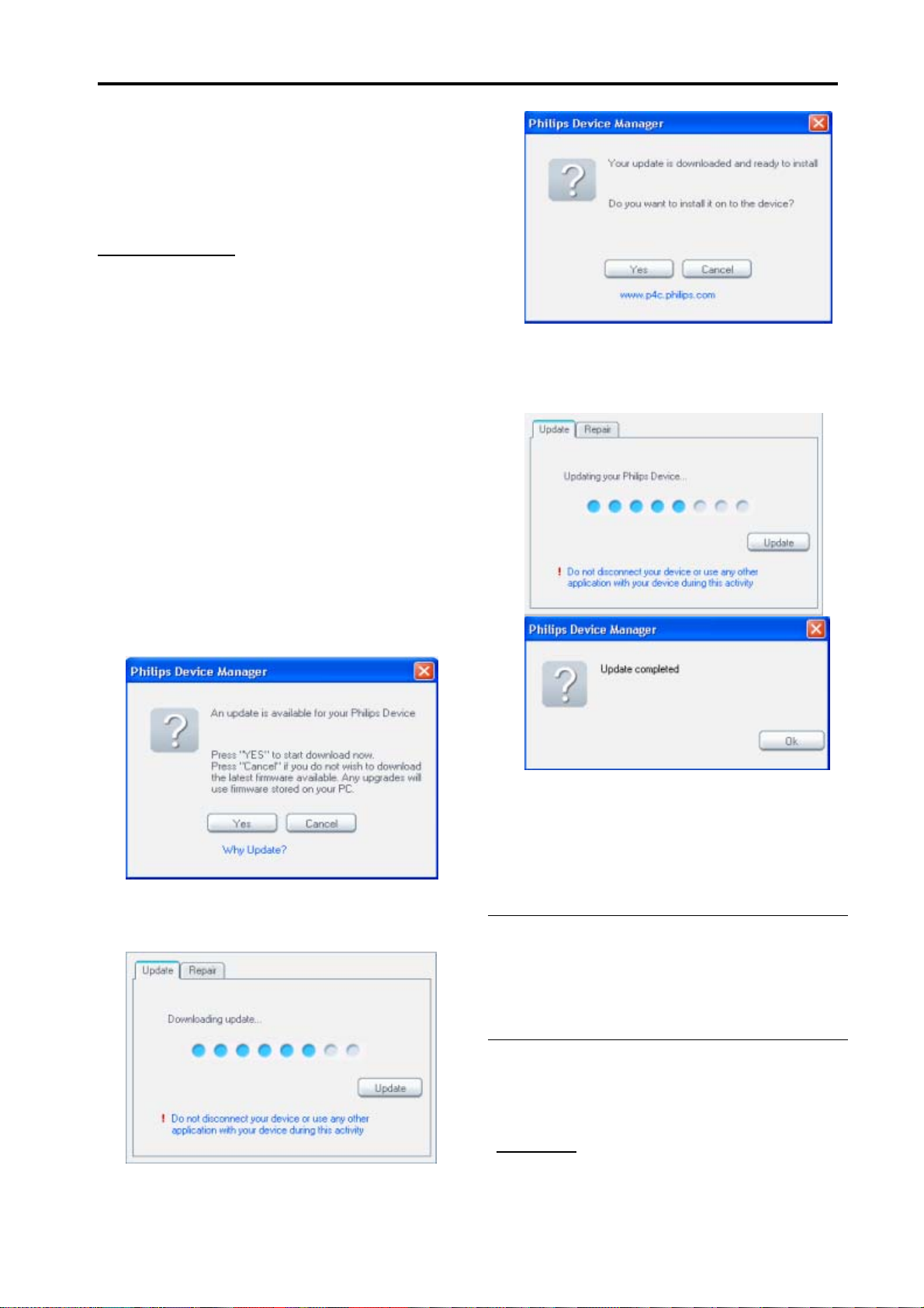
For HDD086/HDD085/HDD082
1. Download the latest version of the Device
Manager application from
http://www.philips.com/support. You may need to
enter your language preference and the model
number e.g.hdd085, to access the Device
Manager application upgrade file.
2. Double click the downloaded execution file to start
the installation of the Device Manager.
3. Connect the GoGear to the po wer supply with the
AC/DC adapter and to the computer with the
provided USB cable. Make sure that Windows
Media Player along with any other applications are
closed.
4. Launch the Philips Device Manag er by double
clicking the Device Manager icon at the task bar
on your computer.
5. Select the REPAIR tab on the dialogue box and
then click Repair to start repairing.
IMPORTANT: All music & content of your micro
jukebox will be erased once the GoGear is
repaired.
icon
6. Once the repair is complete a dialogue b ox will
pop up; click OK and unplug the GoGear from the
computer.
Page 5

1.0 TECHNICAL SPECIFICATION and SERVICE HINTS
Capture the log file from device
1. Switch on the device in FSM mode b y pr essing
and holding the Rec key and then the power
key together.
2. Device will s witch on an d FSM main menu will
be displayed
3. Scroll Down using the key to item 14 HDDinit
4. Press the key, HDD will be initialized, wait till
HDD is initialized, you will get HDD INIT OK
message once initialization is complete
5. Press to display main menu
6. Scroll down using the key to Item 19 Log to
File, press thekey.
7. Wait till writing is completed you will get a
message, writing done
8. Connect USB to device, you will se e a file
LOGINFO.TXT in the root, this is device log
file, size will be around 3KB, copy the file
9. You will also see the pcloginfo.bin in the audio
folder this is the PC log file.
10. Copy both of the above files to PC for future
analysis by the Business if needed.
If the HDD failed the HDDInit test then the device
log may only be read off the LCD display with the
Log to LCD option by following the steps below:
1.
In the FSM main menu scroll down and
select Log to LCD.
2.
Press the key and then when prompted
to “Press RIGHT KEY” message on
display, press the key again you will see
5 parameters at a time on the display and
then press again to see the next 5
parameters.
Page 6

1.0 TECHNICAL SPECIFICATION and SERVICE HINTS
Recovery procedure for flash
corrupt problem
If the device cannot be powered on but it can be
detected by DFU program (device firmware upgrade
application), it can be recovered by following the
procedure below.
Note: Close all applications e.g. Philips Device
Manager before launch the DFU program. Run this
program by Window XP only.
For HDD084 only (MSC mode device)
1. Connect the DFU USB cable to the device first
and then connect to your PC.
2. Launch the DFU program by unzip the
Symphony.rar file and then double click the
DFUAPP.exe file from Symphony folder.
3. Observe the dialogue box to ensure “DEVICE
IS IN DFU MODE”.
4. Select Download and then click Browse to get
the FWImage.ebn file from your PC.
5. Click Start Download to download the firmware
to the device.
6. The program will stop once the successful
message is display.
7. Disconnect DFU USB cabl e from the device.
8. Connect the device to the PC by normal USB
cable and launch the Philips Device Manager to
repair the device. (Download the latest version
of the Device Manager application from Philips
support website http://www.philips.com/support)
Page 7

1.0 TECHNICAL SPECIFICATION and SERVICE HINTS
For HDD086/HDD085/HDD082 (MTP mode device)
1. Unzip the Factory.rar file to your PC. You
should find three folder name “Bootloader”,
“DM” & “Drive_I”.
2. Unzip the Setting.rar file and choose the right
deviceinfo.sec file according to the device
model. Then copy this file into
\Drive_I\UnzipToRoot folder to rewrite the
original deviceinfo.sec file.
8. Disconnect DFU USB cabl e from the device.
9. Open the device, displace will show “BOOT
LOADER APPLICATION Version 4.0”.
10. Connect the device with your PC by normal
USB cable.
3. Connect the DFU USB cable to the device first
and then connect to your PC.
4. Launch the DFU program.
5. Observe the dialogue box to ensure “DEVICE
IS IN DFU MODE”.
6. Select Download and then click Browse to get
bootLoader_HDDXXX.ebn file from
Bootloader folder.
11. Run the install_HDD08x.bat file from Drive_I
folder.
12. Follow all screen instructions to complete the
installation.
7. Click Start Download to download the firmware
to the device. The program will stop once the
successful message is display.
13. Safely remove the device from PC by clicking
on the
device is disconnected from the PC, the display
will show “Firmware Upgrade” for a couple of
icon in your task tray bar. Once the
Page 8
1.0 TECHNICAL SPECIFICATION and SERVICE HINTS
seconds and then start up as usual.
14. Connect the device with PC by normal USB
cable again for MTP connection. Select “Take
no action” once the device is detected by the
PC.
MTP mode installation procedure
after replaced the mainboard
Note: Applicable for HDD085/HDD082 only
Repeat the recovery procedure for flash corrupt
problem from step 9 to 16.
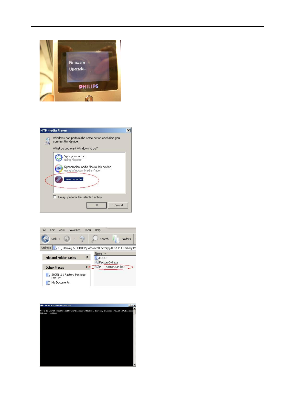
15. Run the MTP_FactoryDM.bat from DM folder to
copy all necessary files into the device.
16. Once the installation is completed, below
dialogue box will auto close.
Page 9

WARNING
GB
All ICs and many other semi-conductors are
susceptible to electrostatic discharges (ESD).
Careless handling during repair can reduce life
drastically.
When repairing, make sure that you are
connected with the same potential as the mass
of the set via a wrist wrap with resistance.
Keep components and tools also at this
potential.
F
ATTENTION
Tous les IC et beaucoup d’autres
semi-conducteurs sont sensibles aux
décharges statiques (ESD).
Leur longévité pourrait être considérablement
écourtée par le fait qu’aucune précaution n’est
prise à leur manipulation.
Lors de réparations, s’assurer de bien être relié
au même potentiel que la masse de l’appareil et
enfiler le bracelet serti d’une résistance de
sécurité.
Veiller à ce que les composants ainsi que les
outils que l’on utilise soient également à ce
potentiel.
2.0 SAFTETY INSTRUCTIONS
ESD
D
WARNUNG
Alle ICs und viele andere Halbleiter sind
empfindlich gegenüber elektrostatischen
Entladungen (ESD).
Unsorgfältige Behandlung im Reparaturfall kan
die Lebensdauer drastisch reduzieren.
Veranlassen Sie, dass Sie im Reparaturfall über
ein Pulsarmband mit Widerstand verbunden
sind mit dem gleichen Potential wie die Masse
des Gerätes.
Bauteile und Hilfsmittel auch auf dieses gleiche
Potential halten.
WAARSCHUWING
NL
Alle IC’s en vele andere halfgeleiders zijn
gevoelig voor electrostatische ontladingen
(ESD).
Onzorgvuldig behandelen tijdens reparatie kan
de levensduur drastisch doen verminderen.
Zorg ervoor dat u tijdens reparatie via een
polsband met weerstand verbonden bent met
hetzelfde potentiaal als de massa van het
apparaat.
Houd componenten en hulpmiddelen ook op
ditzelfde potentiaal.
I
AVVERTIMENTO
Tutti IC e parecchi semi-conduttori sono
sensibili alle scariche statiche (ESD).
La loro longevità potrebbe essere fortemente
ridatta in caso di non osservazione della più
grande cauzione alla loro manipolazione.
Durante le riparazioni occorre quindi essere
collegato allo stesso potenziale che quello della
massa dell’apparecchio tramite un braccialetto
a resistenza.
Assicurarsi che i componenti e anche gli utensili
con quali si lavora siano anche a questo
potenziale.
GB
Safety regulations require that the set be restored to its original
condition and that parts which are identical with those specified,
be used.
NL
Veiligheidsbepalingen vereisen, dat het apparaat bij reparatie in
zijn oorspronkelijke toestand wordt teruggebracht en dat onderdelen,
identiek aan de gespecificeerde, worden toegepast.
F
Les normes de sécurité exigent que l’appareil soit remis à l’état
d’origine et que soient utiliséés les piéces de rechange identiques
à celles spécifiées.
D
Bei jeder Reparatur sind die geltenden Sicherheitsvorschriften zu
beachten. Der Original zustand des Geräts darf nicht verändert werden;
für Reparaturen sind Original-Ersatzteile zu verwenden.
I
Le norme di sicurezza esigono che l’apparecchio venga rimesso
nelle condizioni originali e che siano utilizzati i pezzi di ricambio
identici a quelli specificati.
“Pour votre sécurité, ces documents
doivent être utilisés par des spécialistes agréés, seuls habilités à réparer
votre appareil en panne”.
CLASS 1
LASER PRODUCT
GB
Warning !
Invisible laser radiation when open.
Avoid direct exposure to beam.
S
Varning !
Osynlig laserstrålning när apparaten är öppnad och spärren
är urkopplad. Betrakta ej strålen.
Varoitus !
SF
Avatussa laitteessa ja suojalukituksen ohitettaessa olet alttiina
näkymättömälle laserisäteilylle. Älä katso säteeseen!
3122 110 03420
"After servicing and before returning set to customer perform a
leakage current measurement test from all exposed metal parts to
earth ground to assure no shock hazard exist. The leakage current
must not exceed 0.5mA."
DK Advarse !
Usynlig laserstråling ved åbning når sikkerhedsafbrydere er
ude af funktion. Undgå udsaettelse for stråling.
Page 10

Overview of controls and connections
3.0 Instructions for use
1 USB cable connector
2 p Headphones jack
3 5V DC Charging socket
4 HOLD slider To disable key press
5 LCD display Dynamically displays menu, options and track information
6 VIEW To switch between root menu, library and now playing screens
7 3 / 4 Scroll; SuperScroll; 3 / 4
J( / § Rewind / Fast forward; Up / Down to 1 level / Skip to previous / next
y 2; Power on / off and Play / Pause; confirms a menu setting
8 Neckstrap eyelet
9 Volume + / - Volume control
0 REC Start or Stop Voice recording
! PLAYLIST Add the current track to My Playlist
@ MIC Microphone
3
Page 11

4.0 MECHANICAL INTRUCTIONS
Set Disassembly
1. Remove the Cosmetic screw with an Allen key
2. Use a s crewdriver to carefully lift up the back cover of
the device.
3. Gently open up the back cover.
4. Remove 4 x screws. See arrows
Page 12

4.0 MECHANICAL INTRUCTIONS
5. Open up and remove the bottom part.
6. Remove the battery pack and then the hard disk
7. Take out the 2 screws on the PCB assembly to replace
it from the casing.
Overview of the disassembly parts
Bottom
parts
Back cover
Mainboard /
LCD
module
Top
assembly /
Key set
Hard
Disk
Battery
Page 13

5.0 EXPLODED VIEW & SERVICE PARTS LIST
111
110
108
109
100
105,106
107
103
102
112
101
MECHANICAL PARTS
100 314017750142 FRONT CAB. ASSY HDD084 SILVER
101 314017750591 COVER-REAR LAQ ASSY HDD084 SIL
102 314017750132 REAR CABINET ASSY HDD084
103 314017870131 BATTERY PACK 610MA H LI POLYMER
105 314017900191
314017900231
314017900261
106 314017900121
314017900121
314017800261
107 314017800131
108 282206200083
282206200083
310420052301
282 206200108 HDD086 – HDD 1.0” 4GB
109 314017400331
314017400651
110 314017750321
111 314017750181
112 314017040031
314017320171
PCBA KIT ASSY HDD084/00/05
PCBA KIT ASSY HDD085/00/05
PCBA KIT ASSY HDD086/00/05
PCBA KIT ASSY HDD084/17
HDD082 serial nr. (NW01_ _ _ _ _ _ _ _) PCBA KIT ASSY*
HDD082 serial nr. (NW00_ _ _ _ _ _ _ _) PCBA KIT ASSY*
PCBA KIT ASSY HDD084/97
HDD084/HDD085 - HDD 1.0"3GB 000936-02(CORN)Y
HDD082 serial nr. (NW01_ _ _ _ _ _ _ _) - HDD 1" 3GB*
HDD082 serial nr. (NW00_ _ _ _ _ _ _ _) - HDD 1” 2GB*
DAMPER HDD084
DAMPER HDD082/HDD086
KEYSET-FRONT-ASSY HDD084
LENS-PRI ASSY HDD084
SCREW HEXAGON HDD084
PLATE-PROTECTION
IMPORTANT:
* Please note that there are 2 different execution of HDD082/17 in the market, that
can be distinguished by the serial number with the change code “00” & “01”
please refer to the above table for different applicable PCBA & HDD
MISCELLENEOUS
908210004736 Headphone SHE775BI/00 (for HDD084/HDD085/HDD082)
908210008773 Headphone SHE2550BI/00 (for HDD086)
314017310091 Neck Strap (not for HDD086)
314017400511 Rubber Sleeve (not for HDD086)
272201200608 MOD SUPP AC-DC /00
272201200609 MOD SUPP AC-DC /05
314017830111 AY4108/17 AC/DC Adaptor /17
242207600755 USB CABLE ASSY
314017870361 CD-ROM HDD086
SERVICE TOOL
824041001931 DFU CABLE
Page 14

6.0 FACTORY SERVICE MODE TESTING
Programming the device using for stand-alone FSM
The following is the description for programming the device in stand-alone
mode.
1. Press & hold “ Rec” and then Press together
2. The FSM/DV T application will start and you will see the following
screen.
3. Navigate to the required test.
Using the FSM integrated with UI
Press UP/DOWN key to browse through available tests. Please note that
this action does not activate the test. Press RIGHT key to activate the test
[which is displayed on the screen]. Within a given test LEFT key always
exits from the test back to the test browse screen [Exceptions are Keypad
test, Remote Keypad Test, where test can be exited by 2 short left key
presses].
The following diagram describes the test flow.
<HDD 084>
<FSM/DVT X.X>
<Week XXX>
DOWN
3
5-Key Remote
Test
DOWN
4
SDRAM Read/
Write Test
DOWN
5
SDRAM Self
Refresh Test
DOWN
UP
UP
UP
6
2
LCD and Back
Light Test
LEFT
UP
RIGHT
RIGHT
HDD Test
RIGHT
Perform LCD and
Back Light Test
Perform 5-Key
Remote T e st
LEFT
RIGHT
Perform SDRAM
LEFT
RIGHT
Perform SDRM Self
refresh Test
LEFT
Perform HDD Test
LEFT
DOWN
UP
DOWN
R/W Test
Device Keypad
LEFT short
press (2 Times)
Perform Audio Test
RIGHT
1
Test
Perform Device
KeyPad Test
LEFT
RIGHT
Perform FM Tuner
Test
RIGHT
Device K e y T e s t
LCD B a ck ligh t T e st
5-key Re mote Key Test
SDRAM Read/W rite Test
SDRAM Self-refresh T e s t
HDD T e st
Audio Te s t
FM Tuner Test
Battery L ev e l T e s t
Battery C h a rg ing T e s t
MIC R ec o rd in g T e s t
Real Tim e C lo ck T e s t
. EEPR OM Test
RIGHT
Perform
EEPROMTest
Perform RTC Test
Perform MIC
RecordingTest
Perform Battery
Charging Test
Perform Battery
Level Test
LEFT
LEFT
RIGHT
RIGHT
LEFT
LEFT
RIGHT
RIGHT
DOWN
EEPROM Test
RTC Test
MIC Recording
DOWN
Charging
LEFT
Battery Level
DOWN
Battery
test
UP
13
UP
DOWN
12
UP
11
UP
10
DOWN
UP
9
7
UP
Audio Test
UP
DOWN
FM Tuner Test
8
Page 15

6.0 FACTORY SERVICE MODE TESTING
Test USAGE Description
Power ON screen
Test Browse Screen
Pressing UP/DOWN keys will display names of test cases that can be
selected following are the test cases that are displayed. The current test
that will be selected by pressing RIGHT key will be as shown below.
Note: scroll bar to indicate the test selected can be used provided the
UI+FSM/DVT FW does not exceed 1 MB.
LCD Backlight
> Device Key
5-key Remote Key
LCD Remote Key
<HDD 084>
<FSM/DVT X.X>
<Week XXX>
1. FSM
2. LCD Test
3. Device Keypad Test
4. 5-key Remote Key
5. SDRAM Read/Write
6. HDD Test
7. Audio Test
8. FM Tuner
9. Battery Level
10. Battery Charging
11. Internal MIC Checking
12. RealTime Clock RTC
13. EEPROM Checking
14. Harddisk HDD Initialization
15. Firmware Upgrade
16. Read Device Information
17. Write Device Information
18. Log to file
19. Log to LCD
20. Write to RTC
1.1.3 LCD Back Light Test
Steps
• Scroll to “LCD Test” using UP / Down Key
• Press RIGHT to enter the test. “ LCD Test” is displayed on the LCD.
• Press RIGHT to see the first bitmap
• To view the next bitmap press RIGHT again.
• 4 bitmaps (TBD) are thus displayed and once all the bitmaps are
displayed, it return to the test browser screen, where a next test can
be selected.
• The LCD test can be exited in between the testing process by
pressing LEFT key.
• Pressing “PLAY/PAUSE” Key will turn ON/OFF the Back Light.
• Pressing UP/DOWN Key The contrast level can be changed in steps
of 1 while displaying the test patterns.
Page 16

6.0 FACTORY SERVICE MODE TESTING
• The Test patterns which will be displayed will be as shown
LCD pattern 1: White screen
LCD pattern 2: Black screen with a white square at right upper corner
LCD pattern 3: Checkerboard pattern
LCD pattern 4: Black background
Page 17

6.0 FACTORY SERVICE MODE TESTING
NOTE: The LCD patterns will changed after the new test patterns are
received because the LCD that will be used with HDD084 is black and
white LCD and cannot display greyscale.
Device Key Test
Steps
• Scroll to “Device KEYPAD Test” using UP / Down Key.
• Press RIGHT to enter the test. “ Keypad Test” is displayed on the LCD.
• Press all keys one by one. Every time a key is pressed, the
corresponding key number is displayed as “KEY x DOWN”.
• After releasing the key, KEY x UP is displayed.
• NOTE THAT 2 SHORT LEFT KEY PRESSES CAN EXIT THIS TEST.
• Note: The ADC value will not be displayed on the LCD.
• Once all keys are pressed the test success screen is displayed.
• The Result is indicated as shown
.
<HDD084 Key Test >
< >
<PLAY/PAUSE Up>
< >
<HDD084 Key Test >
< >
<PLAY/PAUSE Down>
< >
<HDD084 Key Test >
< >
<Test S
uccess >
< >
5-Key Remote Control Keys Test
Steps
• Scroll to “ 5-Key REMOTE Key Test” using UP / Down Key
• Press RIGHT to enter the test. “Remote Key Test” is displayed on the
LCD.
• Press all keys one by one. Every time a key is pressed, the
corresponding key number is displayed as “KEY x DOWN”.
• After releasing the key, KEY x UP is displayed.
• Once all the keys are pressed, the test is exited after a brief delay and
the test browse screen will be entered, where next test can be
selected.
• NOTE THAT LEFT KEY PRESSES CAN EXIT THIS TEST.
• Once all keys are pressed the test success screen is displayed.
• The result is as shown
<HDD084 RemoteKey test >
< >
<RC PLAY Up >
< >
<HDD084 Remote Key Test >
< >
<RC PLAY Down >
< >
<HDD084 Remote Key Test >
< >
<Test S
uccess >
< >
Page 18

6.0 FACTORY SERVICE MODE TESTING
SDRAM Read/Write Test
Steps
• Scroll to “SDRAM Read/Write Test” using UP / Down Key
• Press RIGHT to enter the test.
• The test status and results will be shown on LCD. If the test is
successful, “SDRAM R/W TEST OK” is displayed on the LCD and if
the test fails “SDRAM TEST FAIL” will be displayed on the LCD.
• This test can be exited in between the testing process by pressing
LEFT key.
Verification of SDRAM Read Write Functionality
To Verify SDRAM Read Write Functionality Write a pattern 0x55aa55aa to
a specific location and read back the data to verify the data Integrity.
Verification of SDRAM Self-Refresh Functionality
• To verify the SDRAM self-Refresh functionality, we write a string
of characters to the SDRAM and put the SDRAM in self-refresh
mode for 5 Seconds and Check the data integrity before entering
and after leaving Self-refresh mode without any write action on
SDRAM.
<HDD084 SDRAM >
< Self Refresh Test >
<SDRAM Under Test >
< >
HDD084 SDRAM >
< Self Refresh Test >
<SDRAM Self refresh FAIL >
< >
<HDD084 SDRAM R/W Test >
< >
<SDRAM Under Test >
< >
<HDD084 SDRAM R/W Test >
< >
<SDRAM R/W OK >
< >
SDRAM Self-Refresh Test
Steps
• Scroll to “SDRAM Self Refresh Test” using UP / Down Key
• Press RIGHT to enter the test.
• The test status and results will be shown on LCD. If the test is
successful, “SDRAM self refresh TEST OK” is displayed on the LCD
and if the test fails “SDRAM self refresh FAIL” will be displayed on the
LCD.
• This test can be exited in between the testing process by pressing
LEFT key.
Page 19

6.0 FACTORY SERVICE MODE TESTING
HDD Test
Preconditions
• Connect the device to the PC.
Steps
• Scroll to “HDD Test” using UP / Down Key
• Press RIGHT to enter the test.
• The test status and results will be shown on LCD. If the test is
successful, “HDD TEST OK” is displayed on the LCD and if the test
fails “HDD TEST FAIL” will be displayed on the LCD.
• This test can be exited in between the testing process by pressing
LEFT key.
Verification of HDD Functionality
• After connecting it to the PC.
• Create a file “HDD084.txt”.
• Write a predefined sting of characters such as “A-Z”, ”a-z” and “0-
9”.
• Close the file.
• Open it back and read and verify the contents.
• If the contents are same the test has passed else the test is failed.
<HDD084 HDD >
< >
<HDD Under Test >
< >
<HDD084 HDD >
< >
<HDD Test OK >
< >
FM Tuner Test
Precondition
• Ensure that headphones are connected.
Steps
• Scroll to “Tuner Test” using UP / Down Key
• Press RIGHT to enter the test.
• Initialization of the tuner will be done when test is entered.
• Press UP now to search UP in steps of 50kHz.
• Press DOWN to search DOWN in steps of 50kHz.
• Use FUNC1 Key to select manual or auto search mode.
• Whenever a station is found, the frequency and Signal strength are
displayed on the LCD.
• Press PLAY/PAUSE Key to set Stereo Mode. (TBC)
• Press PLAY/PAUSE key to set Mono Mode. (TBC)
• FM recording Test can be performed along with the tuner test as
mentioned in 4.1.14.
• Press LEFT to exit the test, tuner will be disabled and the test browse
screen will be entered where a next test can be selected.
<HDD084 FM TUNER TEST>
< F106.50 S3 >
<MODE STEREO/MONO >
< >
Page 20

6.0 FACTORY SERVICE MODE TESTING
Battery Level Test
Steps
• Scroll to “Battery Test” using UP / Down Key
• Press RIGHT to enter the test.
• Battery level is displayed on the screen in Volts
• Battery Level will be refreshed regularly every 1 sec.
• If the battery level is lesser than 2.8 V a “LOW BATTERY” warning
will be flashed on the LCD for 10 seconds and the device goes to
shutdown mode (TBD).
• Press LEFT key to exit the test.
• Note this test should be done without initialising the HDD.
<HDD084 BATTERY LEVEL TEST>
< X.XXXV >
<CAL.STATUS >
< >
Battery Charging Test
Steps
• Scroll to “Battery Charging test” using UP / Down Key
• Press RIGHT to enter the test
• Press LEFT to exit the test
• The charging current is updated every 1 seconds
• If charging current is less than 20mA, battery is not in the charging
status.
• The following tale indicates the charge current for different states
CHG_STATUS
(GPA4)
CHG_CURRENT INDICATION ON
THE LCD
H X Charge Up
L <20mA Charge Up
L > = 20mA Charging
• The Following information is displayed on the LCD.
NON-USB CHARGING MODE
<HDD084 BATTERY CHARGING TEST>
< X.XXXV YYY.YmA >
<CHG.STATUS >
< Adaptor STATUS >
>
USB CHARGING MODE
If the USB connection is made the system will startup in the low power
mode (trickle charging – <100mA include system current) and after the
enumeration process, SW can decide whether high power mode can be
switched on for a fast charging - <500mA include system current.
<HDD084 BATTERY CHARGING TEST>
< X.XXXV YYY.YmA >
<CHG.STATUS >
< USB STATUS >
>
Page 21

6.0 FACTORY SERVICE MODE TESTING
• The battery level will be refreshed regularly every 1 second.
MIC Recording Test
• The recoded file can be verified in “AUDIO TEST CASE” (4.1.9)
• Press LEFT to exit the test.
Steps
• Connect a microphone.
• Scroll to “MIC Recording Test” using UP / Down Key
• Press RIGHT to enter the test.
• Press REC key to start the recording .The recorded file will be
“MICREC.MP3”.
• The recoded file can be verified in “AUDIO TEST CASE” (4.1.9)
• Press LEFT to exit the test
FM Recording Test
Steps
• This test will be done during the tuner test and is not a separate test
• Initialise the Tuner.
• Search the desired station using UP/DOWN Key.
• Press REC key to start the recording .The recorded file will be
<HDD084 MIC RECORDING >
< >
<REC ON >
< >
case .
“FMREC.MP3”.
<HDD084 FM RECORDING >
< F106.50 S3 >
<STEREO >
< REC ON >
Real Time Clock Test
Steps
• Scroll to “Real Time Clock Test” using UP / Down Key
• Press RIGHT to enter the test. “
• If the test is successful “RTC TEST OK” is shown on LCD, if the Test
fails “RTC TEST FAIL” is shown on the LCD.
• Press LEFT to exit the test.
.
Verification of RTC
• When user selected the RTC test, Software will write a pre-defined
register value to the RTC.
• After 1 second, Software will read back the RTC register value
and check if the RTC date is correct and clock is incremented by 1
second.
• If the test is successful, “RTC TEST OK” is shown on the LCD
display, if test fails “RTC FAIL” is shown on the LCD display.
.
Page 22

6.0 FACTORY SERVICE MODE TESTING
<HDD084 EXTERNAL RTC >
< >
<RTC under Test >
< >
EEPROM Test
Steps
• Scroll to “EEPROM test “using UP / Down Key
• Press RIGHT to enter the test. “
• If the test is successful “EEPROM TEST OK” is shown on LCD, if the
test fails “EEPROM TEST FAIL” is shown on the LCD.
• Press LEFT to exit the test.
Verification of EEPROM Functionality
To Verify EEPROM Functionality Write a pattern 0x55aa55aa to a specific
location and read back the data to verify the data Integrity, repeat the
write/read test by pattern 0xaa55aa55.
<HDD084 EXTERNAL RTC >
< >
<RTC Test Ok >
< >
Steps
Powering Off
• Pressing play key for longer than 2 seconds causes system power off.
• Release the PLAY key once “OFF” is displayed in the LCD. Note that
system is shutdown only after release of PLAY key.
• System can be powered off while any test case is being executed.
• System can again be powered on by pressing play key and holding for
2 seconds
< HDD084 >
< >
< POWER OFF >
< >
Appendix I
Firmware Upgrade
Steps
<HDD084 EEPROM TEST >
< >
<EEPROM under Test
>
< >
<HDD084 EEPROM TEST >
< >
<EEPROM Test Ok
>
< >
• Select the test and press right key to enter the test
• Firmware upgrade can be done by copying a hdd084_FSM.ebn
file from a specified directory I.e. “_system” on HDD
• The device copies the firmware image into the device
NOTE: this test should be done after initializing the HDD
Page 23

6.0 FACTORY SERVICE MODE TESTING
HDD initialisation
Steps
• Select the test and press right key to enter the test
• Initialize the HDD
Page 24

7.0 OVERALL BLOCK DIAGRAM
Cornice
3GB Hard Disk
HDD Connector
Cornice
TIC
HDD084 BLOCK DIAGRAM
(V1.2)
(2005-05-09)
Analog keys
on the 5-key Remote
SDRAM
Analog Keys on the
Device
USB Mini-B Socket
USB_SUSPEND
USB_HIGH_PWR
CHG_STATUS
BATT_LOW_N
Power On
PWR_ACK
logic
PMU
LTC3455
AC/DC Input Jack
Reverse +
Overvoltage
protection
Constant
Current
Source
1 Cell Li-polymer
Battery
Battery Connector
MultiICE connector
+ mode selection
switches
Symphony
UART
JTAG
GPIO
LCD_BL_CTRL
LCD Interface
LCD Connector
LCM
96x64
B/W
12MHz
sysclock
EEPROM
M24C08
RTC
32KHz
RTCclock
Memory Bus GPA
Symphony
PNX0102
interface
RTC_OUT
I2C
LNA
MIC
amplifier
MIC
FM tuner
Line In
Line Out
FM_ANT
USB2.0
Headphone
Out
Headphone
connector
High
Speed
GPIO
GPA
Reset
1V8 3V1
BAT_LEVEL
CHG_CURRENT
Reset
logic
VBacklight
LDO
3V0_A
EXTERNAL DEVICES
HDD084 Only, not for
3V0_RF
LEGEND
BOARD
COMPONENTS
CONNECTORS
PSA610
LDO
Page 25

1 2415
8.0 ELECTRICAL DIAGRAM
2 3
4
5 23
6
7
8 9
10
11 19
12 16
13
14
17
20
2118
22
25 28
26
27
A
1300 F2
1400 J5
1401 F6
B
1402 D6
1403 D11
1404 I8
1405 K1
1406 J20
C
D
A
E
B
F
C
G
D
H
I
E
J
F
K
G
L
H
M
N
I
O
J
P
is prohibited without the written consent of the copyright
All rights reserved. Reproduction in whole or in parts
owner.
K
Q
L
1407 J18
1408 C4
1409 A4
1411 C5
1412 D6
1413 E3
1414 E4
1415 E4
KEY_UP
KEY_PLAY
FM_ANT
RXD
RTC_INT
IIC_SCL
IIC_SDA
1416 E5
1417 C4
1419 A14
2300 F6
2301 G6
2302 G3
2303 G4
2304 G5
2305 G6
2306 G4
2307 G3
2308 G4
2400 L6
2401 B8
2402 C7
2403 E7
2404 D11
2405 D11
2406 E8
2407 F9
2408 F9
2409 F8
2410 F8
2412 C12
2413 E11
2414 B12
2415 B12
2416 B13
2418 B13
2419 B13
2420 B14
2421 B14
2422 B14
2423 B14
2424 G7
2425 G7
2426 G9
2427 G9
2428 H7
2429 H8
2430 G8
2431 H8
2432 J3
2433 J1
2434 K1
2435 B18
2436 B18
2437 B18
2438 B18
2439 B19
2440 B19
2441 B19
2442 J15
2443 H20
2444 K15
2446 F11
2447 K15
2451 C4
2452 C4
2456 L7
2457 C5
2459 C5
2461 C6
2470 L7
2471 L6
2472 L7
2473 L6
2474 L7
2475 L6
2476 A13
2477 A15
2478 A15
2479 A16
2480 A17
2481 K6
2482 K6
2483 L6
2484 K17
2486 C7
2493 E3
2494 D4
2495 D4
2496 D5
2497 D6
2498 D7
2499 L6
3300 F5
3301 G5
3302 G6
3303 G6
3304 F4
3305 F5
3306 G5
3401 B7
3402 D7
3403 H14
3404 E9
3405 F8
3406 C12
3407 G7
3408 I17
3410 F7
3411 F7
3412 H1
3413 H1
3414 H2
3415 H2
3416 I2
3417 I10
3418 J9
3419 K10
3420 K11
3421 J2
3422 H3
3423 I3
3424 H5
3425 G14
3426 G14
3427 I5
3428 H16
3429 H16
3430 H16
3431 H14
3432 H15
3433 I14
3434 K14
3436 J15
3437 J16
3447 J6
3448 J4
3449 K2
3450 K1
3451 I12
3452 A3
3453 A7
3454 A7
3455 C1
3456 B5
3457 B5
3458 B6
3459 B7
3460 B4
3461 D4
3462 D4
3463 D5
3464 D7
3465 E7
3466 D6
3467 I20
3468 I20
3469 I7
3470 I7
3471 I15
3472 I15
3473 I12
3474 I12
3475 I12
3476 I12
3477 F16
3478 H14
3479 H17
3480 H14
3481 H15
3482 J16
3483 K15
3486 F14
3491 A14
3492 A15
3493 C7
3494 C7
3495 E6
3496 I19
3498 I16
3499 A10
4400 H7
4401 I7
4402 J5
4403 J5
4405 G12
4406 C13
4407 D11
4408 E12
4409 E8
4410 F15
4411 F15
4412 F15
4413 F15
5300 F3
5301 G3
5302 F4
5303 G4
5304 G2
5305 F3
5400 J17
5403 J6
5404 A17
6103 E2
6400 K18
6401 K19
6402 K19
6403 B2
6404 B3
6405 D2
6406 D3
6407 C3
6408 H3
6409 G1
6411 I5
7401 J2
7402 I20
7410 A6
7411 E18
7412-1 E6
7412-2 E5
7413 A16
7414 A10
7415 D12
7417-1 C7
7417-2 C6
7418-1 H2
7418-2 H2
7419 H4
7420 I4
7421 H5
7422 H5
F001 K8
F002 K9
F003 K9
F004 K10
F005 K10
F006 K10
F401 J4
F402 K2
F403 I4
F404 F15
F405 F15
F409 J11
F410 J11
F411 E3
F412 E4
F413 E5
F414 E6
F415 G14
F416 E6
F417 A11
F420 H17
F421 H17
F422 A3
F423 E2
F424 B9
F425 B9
F426 D8
F430 G14
F432 H16
F433 C4
F434 C5
F435 C5
F436 C6
F437 C6
F480 G2
F481 G2
F482 G2
F483 I8
F484 I8
F485 I8
F486 I8
F487 J8
F488 J8
F489 J8
F490 J8
F491 A15
F492 E8
1 2 3 4 5 6 7 8 9 10 11 12 13 14 15 16 17 18 19 20 21
KEY_VOL_UP
VREF_KEY
10K
3455
KEY_INT
KEY_PLAY_RST
PGB
6409
150V
RF_GND
3412
47K
2433
12p
2434
12p
1405
3450
100R
BAT54 COL
V3V0_A
3413
F402
BAT54 COL
F423
TC38-360-33-TR
3414
100K
32K768
3449
100R
6405
6403
1300
18K
7418-1
BC847BPN
2
V3V3_D
3421
BAT54C
1
2
4
3
BC847BPN
100K
1
2 OSCO
3 INT_
6 SCL
6103
F480
F481
F482
5304
RF_GND
7418-2
4
5
6
1
6K8
3416
7401
PCF8563TS
OSCI
SDA5
BAT54 COL
BAT54 COL
HP_OUTR
HP_OUTL
1u0
3
32.768kHz
VOLTAGE
DETECTOR
MONITOR
INTERFACE
VSS
4
3415
OSC
OSC
I2C
KEY_HOLD
6404
6406
6408
BAS316
1K0
VBAT
8
VDD
BUS
6407
BAT54 COL
2n2
2493
5305
5300
5301
2432
100n
CLKO
DIVIDER
CONTROL
LOGIC
POR
ADDRESS
REGISTER
VREF_KEY
3452
100K
4
6
1408
2n2
1%22K
1414
SKQY
2306
2308 330p
RF_GND
LCD_RST_N
RSTIN_N
2K2
F401
5
7
F412
3304
1K0
4n7
2303
F422
1413
2302
RF_GND
7
SKQY
3
2
1
2451
3461
2n2
F411 F413
330p2307
4n7
RF_GND
3422
330R
7419
BC817-40W
3423
330R
7420
BC817-40W
V3V3_D
3448
CONTROL/STATUS1
CONTROL/STATUS2
SECONS/VL
MINUTES
HOURS
DAYS
WEEKDAYS
MONTHS/CENTURY
YEARS
MINUTE ALARM
HOURS ALARM
DAY ALARM
WEEKDAY ALARM
CLKOUT CONTROL
TIMER CONTROL
TIMER
F433
SKRE
1409
SSSS8
3462
24952494
2n2
4n7
F403
RTC_OUT
3460
22K
1%
2452
2n2
5302
5303
1%10K
1415
F434
1417
SKRE
3463
6K8
2496
2n2
SKQY
KEY_REMOTE_IN
3305
8R2
3306
8R2
4402
4403
1400
27FX-RSM1-S-TB
1
2
3
4
5
6
7
8
9
10
11
12
13
14
15
16
17
18
19
20
21
22
23
24
25
26
27
2829
3456
10K
1%
2457
3424
330R
1%
7421
BC817-40W
3427
330R
F435
1411
7412-2
BC847BS
7422
BC817-40W
6411
BAT54 COL
2459
SKRE
1416
3300
8R2
3301
8R2
2n22n2
SKQY
KEY_REMOTE_IN
3457
6K8
1%
3
4
F414
4n7
2304
V3V3_D
3458
3K3
1%
2461
3
2n2 2n2
4
7417-2
BC847BS
F436
1412
SKRE
3466
1%
3K3
2497
2n2
3495
5
470K
7412-1
BC847BS
1401
4n7
3302
V3V3_D
10K
5403
10K
2305
3447
5
6
1
SKQY
3303
VIN_R
VIN_L
7410
BC847B
6
BC847BS
1
1402
2
F416
2300
6.3V220u
2301
6.3V220u
10K
1u02481
2482 1u0
1u02483
100n
2471
100n2473
VREF_KEY
7417-1
F437
SKRE
3464
2498
2n2
2470 100n
2472 100n
2474 100n
2
3459
2486
3453
1K0
1%
2
1
1%1K0
3465
470K
4400
4401
10K
3
3493
470K
3494
470K
2424
VREF_KEY
V3V0_A V3V0_A
3410
100K
V3V0_A
10u
2425
100n
1M0
3469
3470
LCD_RW_WR
LCD_E_RD
LCD_D(0)
LCD_D(1)
LCD_D(2)
LCD_D(3)
LCD_D(4)
LCD_D(5)
LCD_D(6)
LCD_D(7)
10R
2428
LCD_CS
LCD_RS
VREF_KEY
1%
10K
3454
F426
VREF_KEY
F492
3405
150R
V1V8_D
2430
1404
9
8
7
6
5
4
3
2
1
2n2
2401
KEY_INPUT_LINE1
2406
1u0
2409
100n
2410
22u 6.3V
V3V0_A
2431
F483
F484
F485
F486
F487
F488
F489
F490
100n
100n
VREF_KEY
1%
10K
3401
2n2
2402
VREF_KEY
1%
10K
3402
2n2
2403
V3V0_A
4409
V3V0_A
3411
100K
3407
10u
100n
2429
{LCD_RW_WR,LCD_E_RD,LCD_D(0:7),LCD_CS,LCD_RS}
1M0
10FMN-BMT-A-TFT
10
F001
F425
V3V0_A
GPIO_2
1V8_PROG
2426
F424
10u
F002
2427
3404
10R
100n
3418
2407
100K
F003
NCP305LSQ28
2
RST-OUTPVIN
EXTERNAL_5KEY_RC
KEY_INPUT_LINE2
10u
2408
100n
LCD_RW_WR
LCD_E_RD
LCD_D(0)
LCD_D(1)
LCD_D(2)
LCD_D(3)
LCD_D(4)
LCD_D(5)
LCD_D(6)
LCD_D(7)
LCD_CS
LCD_RS
IIC_SCL
IIC_SDA
RSTIN_N
F004
7414
GND
4NC3
BAT_LEVEL
CHG_CURRENT
V3V3_D
3417
100K
V3V3_D
F005
VREF_KEY
3492
1K0
V3V0_A
F491
2478
10u
2479
100n
4
7413
NCP500SN30
ENABLE
VOUTNCVIN
GND
2
3
15
1u0
2480
1
10K
3499
F417
RTC_OUT
RC_INT
4407
56K
V1V8_D
3406
2R2
V1V8_D
2412
2414
100n
PNX0102AET
100n
7415
2415
2416
100n
V1V8_D
H1
V11
VDDI
100n
4406
V16
MIC_IN
V3V3_D
V3V3_D
E1
V5
2476
1u0
2418
V14
VDDE
KUF4523
100n
J18
A16
1419
2419
A7
2
100n
+
2420
1
100n
2421
100n
2422
3491
2K2
100n
2423
100n
2477
47u 6.3V
5404
V3V3_D
V3V3_D
2435
100n
2436
100n
2437
100n
2438
100n
2439
100n
2440
100n
2441
100n
MPMC_D_(0:15)
MPMC_A_(0:14)
{SD_CLK,SD_CKE,SD_DQM1,SD_DQM0,SD_RAS,SD_CAS,SD_CS,SD_WE}
Φ
SOLID STATE
IN
OUT
VDDA18
VSSA
IN
OUT
VDDA18
VSSA
IN
VDDA33
GNDA
0
1
2
GPA
3
4
VDDA33
GNDA
R
VOUT
L
VDDA33
P
VREF
N
R
OUT
L
A
OUTC
B
VDDA33A
VDDA33B
GNDAA
GNDAB
MIC_LNA
VCOM
P
REF
N
VDDA18
VDDA33
GNDA
VREF
VINR
VINL
MIC
RW_WR
E_RD
0
1
2
3
DB LCD
4
5
6
7
CSB
RS
0
1
DAT
2
3
CLK
CMD
BCK
WS
DATA
CLK
BCK
WS
DATA
TRST
TCK
TMS
TDI
TDO
SEL_ARM
SCL
SDA
RSTIN
FLASH_VDD_HV
AUDIO
XTALH
XTALL
SPDIF
ADC10B
DAC
HP
ADC
MCI
DAI
DAO
JTAG
IIC
VSSI VSSE
G1
V12
V17
MPMC
UART
DCDC
USB
VDDA33_DRV
F1
V6
D
A
STCS
DYCS
CLKOUT
CKE
WE
RAS
CAS
DQM
OE
BLOUT
RPOUT
TXD
RXD
CTS
RTS
GPIO
PLAY
STOP
LX1
LX2
VUSB
VBAT
VOUT33A
VOUT33B
VOUT18
VSS1
VSS2
GND
CLEAN
RPU
DP
DM
VBUS
RREF
GNDA
VSSA_REF
VSSA_TERM
VDDA18_PLL
VDDA18_BG
VDDA13
A6
A15
V13
H18
A1
0
A2
1
B2
2
A3
3
A4
4
B4
5
A5
6
B5
7
C4
8
C5
9
C6
10
B6
11
C7
12
B7
13
C8
14
B8
15
E16
0
E17
1
E18
2
D16
3
D17
4
D18
5
A18
6
B18
7
C18
8
B17
9
C17
10
B16
11
C16
12
B15
13
C15
14
A14
15
B14
16
C14
17
A13
18
B13
19
C13
20
C9
0
A8
1
B11
2
B9
A10
B10
C11
A9
C10
C12
0
A11
1
A17
A12
0
B12
1
B1
L3
K3
K2
K1
K16
0
K17
1
K18
2
J16
3
L17
L18
P17
N17
T18
M17
R18
M16
N18
P18
N16
L16
M18
T15
U17
T17
U14
P16
R17
R16
T16
U15
U16
U18
V18
F430
MPMC_D_(0)
MPMC_D_(1)
MPMC_D_(2)
MPMC_D_(3)
MPMC_D_(4)
MPMC_D_(5)
MPMC_D_(6)
MPMC_D_(7)
MPMC_D_(8)
MPMC_D_(9)
MPMC_D_(10)
MPMC_D_(11)
MPMC_D_(12)
MPMC_D_(13)
MPMC_D_(14)
MPMC_D_(15)
3486
3426 1K0
F415
1K03403
1K03478
3431
3480
3433 1K5 1%
3434
MPMC_A_(0)
MPMC_A_(1)
MPMC_A_(2)
MPMC_A_(3)
MPMC_A_(4)
MPMC_A_(5)
MPMC_A_(6)
MPMC_A_(7)
MPMC_A_(8)
MPMC_A_(9)
MPMC_A_(10)
MPMC_A_(11)
MPMC_A_(12)
MPMC_A_(13)
MPMC_A_(14)
1K0
1K03425
1K0
1%
12K
F404
F405
BATT_RD_EN
CHG_STATUS
1K0
3432
3481 1K0
3471
2447
MPMC_A_(13)
MPMC_A_(14)
4412
4413
ATA_DMARQ
BATT_LOW_N
HD_PWR_N
1K0
3472
100K
2442
100n
1u0
2444
100n
4410
4411
SD_CS
SD_CLK
SD_CKE
SD_WE
SD_RAS
SD_CAS
SD_DQM0
SD_DQM1
RC_INT
USB_HIGH_PWR
LCD_RST_N
USB_SUSPEND
LCD_BL_CTRL
100K
3436
2R2
3483
2R2
V3V3_D
V1V8_D
3477
1K0
ATA_CS0
ATA_CS1
ATA_INTRQ
V3V3_D
10K
3428
3430 100R
V3V3_D
3498
3437
RXD
F432
1M0
100K
100R3429
3482
56K
SD_CLK
SD_CKE
SD_CS
SD_RAS
SD_CAS
SD_WE
F420
F421
3479 1K0
3408
56K
MPMC_A_(0)
MPMC_A_(1)
MPMC_A_(2)
MPMC_A_(3)
MPMC_A_(4)
MPMC_A_(5)
MPMC_A_(6)
MPMC_A_(7)
MPMC_A_(8)
MPMC_A_(9)
MPMC_A_(10)
MPMC_A_(11)
MPMC_A_(12)
MPMC_A_(13)
MPMC_A_(14)
VUSB
2484
MT48LC16M16A2
UART_TXD
UART_RXD
GPIO_2
PWR_ACK
1V8_PROG
5400
100n
7411
23
0
24
1
25
2
26
3
29
4
30
5
31
6
32
7
33
8
34
9
22
10
35
11
36
12
20
0
BA
21
1
38
CLK
37
CKE
19
CS
18
RAS
17
CAS
16
WE
MMBZ15VALT1
14
1
VDD
0
A
4M-1
VSS
28
41
6400
V3V3_D
27
3
9
VDDQ
Φ
DRAM
4M X 16 X 4
VSSQ
6
54
12
1407
DLW31S
43
49
40
NC
2
0
1
2
3
4
5
6
7
D
8
9
10
11
12
13
14
15
H
DQM
L
46
52
V3V3_D
10K
3496
1
2
3
43
12
6401
MPMC_D_(0)
4
MPMC_D_(1)
5
MPMC_D_(2)
7
MPMC_D_(3)
8
MPMC_D_(4)
10
MPMC_D_(5)
11
MPMC_D_(6)
13
MPMC_D_(7)
42
MPMC_D_(8)
44
MPMC_D_(9)
45
MPMC_D_(10)
47
MPMC_D_(11)
48
MPMC_D_(12)
50
MPMC_D_(13)
51
MPMC_D_(14)
53
MPMC_D_(15)
39
15
(1Kx8)
EEPROM
NC1
NC2
E2 SDA
ADR
PGB
6402
150V
SD_DQM1
SD_DQM0
V3V3_D
M24C08-WDW6TP
84
Φ
PGB
150V
2443
WC
SCL
100n
7402
7
6
5
1406
TCX0101-110177
1
2
3
4
5
6 7
8 9
3467 100R
100R
3468
3419
F006
1403
22p
2404
2K7
2K7
3420
hole-pth-0150
12M
2405
MIC_IN
ATA_IORDY
ATA_RESET
BURST_DIS
V1V8_D
22p
2413
V3V0_A
2446
ATA_IOWR
ATA_IORD
KEY_HOLD
TIC_CLK
RTC_INT
KEY_INT
TIC_OFF
EXT_DC
F409
F410
100n
100n
3451 1K0
3473 1K0
3474
3476 1K0
4408
V1V8_D
4405
1K03475
100K
1K0
T10
V9
U9
T9
V7
T8
U8
V8
T12
U11
T11
U7
T7
U6
T6
U5
V10
U10
M3
M2
L1
L2
M1
P3
N3
N2
N1
R1
R2
P2
P1
T2
T3
U2
V1
V3
U3
V2
U1
T1
T4
R3
G2
F2
C2
C1
C3
D2
D1
D3
E2
E3
B3
F3
H3
J2
J1
J3
G3
H2
H17
G17
G16
F16
G18
F18
F17
T13
V4
U12
T5
U13
U4
H16
J17
T14
V15
IIC_SCL
IIC_SDA
A
B
C
D
E
F
G
H
J
K
L
A
B
C
D
E
F
G
H
I
J
K
L
M
I
N
O
P
Q
R
toestemming van de auteursrechthebbende.
gedeeltelijk, is niet toegestaan dan met schriftelijke
Alle rechten voorbehouden. Verveelvuldiging, geheel of
S
T
1
2499
470p
2400
100n
2475
1u0
2456
1u0
R
1
2 3 4 5 6 7 8 9 10 11 12 13 14 15 16 17 18 19 20 21
S
HDDSETNAMECHN
CLASS_NO
3PC330
1
2004-12-10
2005-04-12
NAME
RAYMOND CHOI
2
3
4
5 16
6
7 8
9
10
11 12
13 15
14
17
18 22
19
20
21
2
3
23
PBAS HDD084
HDD084
SUPERS.
2004-06-11
DATECHECK
24
25
3140 178 0012
130
4
C
KONINKLIJKE PHILIPS ELECTRONICS N.V. 2004
1
26
1
1
1
1
1
2005-04-12
2005-03-24
2005-03-07
2004-12-10
2004-09-23
2827
T
A1
Page 26

1
8.0 ELECTRICAL DIAGRAM
3
5
6
7
84
9
10
112
12
13
14
15
16
17
18
19
20
1410 E13
1418 E4
A
2137 I13
B
A
C
D
B
E
C
F
D
G
H
E
I
F
J
K
is prohibited without the written consent of the copyright
owner.
All rights reserved. Reproduction in whole or in parts
G
L
H
M
I
N
2139 G12
2140 G12
2411 E12
ATA_DMAACK
2448 E4
2449 D11
2450 E12
2453 I12
2454 I12
2455 I12
2458 I13
2460 I13
2462 I13
2463 I14
2464 D3
2465 D5
2466 D10
2467 D9
2468 E3
2469 B2
2487 G5
2488 E13
2489 G12
2490 G3
2491 D5
2492 D10
3438 A6
3439 B3
3440 C5
3441 E4
3442 D5
3443 E4
3444 C3
3484 B3
3485 F3
3487 C4
3488 C4
3489 C8
3490 B5
4404 D9
5401 E12
7403-1 H9
7403-2 A7
1 2 3 4 5 6 7 8
V3V3_D
V3V3_D
J12
B12
A13
A12
B11
A
CS
DMA
NC
CLK
B2
M8
7403-2
TIC-001829-01
Φ
HOST
REVERSE
CF-PF="0"
D
DASP
PDIAG
INTRQ
PG
A5
0
B5
1
B4
2
J13
3
H12
4
G12
5
E13
6
C12
7
A4
8
A3
9
A2
10
11
G13
12
F13
13
D13
14
C13
15
E12
F12
A9
N13
CLOCK &
CONTROL
H2
0
EMU
H1
1
JTAG
{SE_NRZD(0:7),SE_NRZDC,SE_SG,SE_RG-WG,SE_DATA,SE_CLOCK,SE_SSM-ERR}
SE_NRZD(0) SE_NRZD(1)
SE_NRZD(1)
SE_NRZD(2)
SE_NRZD(3)
SE_NRZD(4)
SE_NRZD(5)
SE_NRZD(6)
SE_NRZD(7)
V3V3_D
2469
100n
4
7416
74AHC1G32GW
F440
1
2
3 5
HD_PWR_N
V3V3_D
3439
3484
TIC_CLK
100K
100K
ATA_IORD
ATA_IOWR
3444
10K
2468
3485
33R
2464
100n
2
18p
V3V3_D
NC
1
3441
1418
2490
C11
C5
D4
D3
C3
C4
L7
L6
L5
L4
L3
L11
K3
K11
J3
J11
H3
H11
G11
F2
E11
E3
1M0
7409
BC857B
5
1
12M
5p6
NC
ATA_DMARQ
ATA_RESET
ATA_IORDY
74LVC1GU04
4
3
3443
2448
TIC-001829-01
7406
1K0
18p
7403-5
Φ
DSP
3488
3487
100K
TIC_OFF
7405
74LVC1G14GW
15VCC
L10
M11
NCNC
M12
K10
D10
D11
C10
V3V3_D
M6
M5
M4
M3
M7
L9
L8
C6
C9
3490
100K
NC
A2
GND
3
100K
F460
Y 4
MPMC_A_(10)
MPMC_A_(11)
MPMC_A_(12)
ATA_CS0
ATA_CS1
V3V3_D
3440
2465
100n
3442
33R
SE_SSM-ERR
SE_CLOCK
SE_DATA
SE_RG-WG
SE_SG
SE_NRZDC
F459
100K
V3V3_D
2487
10K
3438
5p6
2491
F441
7403-3
TIC-001829-01
Φ
SE
NORMAL
SE-PINFLIP="1"
F11
SE-PINFLIP
M1
SSM-ERR
N1
CLOCK
N2
DATA
N3
RG-WG
N4
SG
M13
NRZDC 7
100n
7403-4
TIC-001829-01
C2
D2
D1
E2
E1
F1
L12
F493
L13
GPIO-7
K12
GPIO-8
K13
M9 C7
L2
M2
NC
NC
NC
GPIO
TEST
Φ
C8
CF-PF
B6
0
B7
1
B8
2
D12
0
B13
1
A7 H13
ACK
A6
RQ
B9
RESET
A10
RD
B10
WR
A8
RDY
B3
CS16
G1
1
G2
2
F3
SEL
C1
IN
B1
RST
M10
TICOFF
A1
INH-PG
L1
TMS
K2
TRST
K1
TDI
J2
TDO
J1
TCK
N5
0
N6
1
N7
2
N8
3
NRZD
4
5
6
NC
GPIO-C
NC
GPIO-E
NC
NC
N10
N11
N12
N9
MPMC_D_(0)
MPMC_D_(1)
MPMC_D_(2)
MPMC_D_(3)
MPMC_D_(4)
MPMC_D_(5)
MPMC_D_(6)
MPMC_D_(7)
MPMC_D_(8)
MPMC_D_(9)
MPMC_D_(10)
MPMC_D_(11)
MPMC_D_(12)
MPMC_D_(13)
MPMC_D_(14)
MPMC_D_(15)
3489
V3V3_D
7403-3 F6
7403-4 H6
7403-5 H4
100K
PWR_ACK
A11
D7
E4
G4
H10
K5
K6
G3
K7
G10
D8
7405 D5
7406 D4
7408 C11
ATA_INTRQ
TIC-001829-01
SUPPLY
VDDSHV
VDDSHVREG
7409 C4
7416 C2
9 10
MPMC_D_(0:15)
VBAT
4404
1u0
2466
2467
7403-1
Φ
VSS
E10
F10
J10
D5
D6
D9
F4
H4
J4
K4
K8
K9
F441 E6
F442 E12
F443 F12
10n
2492
8
3
5
100p
F444 G13
F445 F11
F446 F11
TPS73633DRBR
IN
NR
FB
EN
7408
Φ
4
SE_NRZDC
SE_NRZD(7)
SE_NRZD(6)
SE_NRZD(5)
SE_NRZD(4)
SE_NRZD(3)
SE_NRZD(2)
SE_NRZD(0)
SE_SG
SE_RG-WG
SE_DATA
SE_CLOCK
SE_SSM-ERR
F447 F11
F448 F11
F449 F11
F450 F11
F451 F11
F452 F11
F453 F11
F454 F11
F455 F11
F456 G11
F457 G11
F458 G11
F459 B5
F460 C5
F493 H5F440 B2
A
11 12 13 14
B
A
C
B
D
E
C
1
OUT
2
6
NC
7
HS_GNDGND
9
2449
10u
D
F
G
V3V3_HDD
5401
F442
H
E
6.3V220u
2140
F443
6.3V220u
2411
22u 6.3V
20FLH-SM1-TB(LF)(SN)
F444
2489
100n
1410
21 22
100n
2488
20
19
18
17
16
15
14
13
12
11
10
9
8
7
6
5
4
3
2
1
F
G
I
J
K
F445
F446
F447
F448
F449
F450
F451
F452
F453
F454
F455
F456
F457
F458
2450
100n
2139
L
V3V3_D
H
M
2453
100n
2454
2455
100n
2458
100n
2460
100n
2137
100n
2462
100n
2463
100n
100n
I
N
gedeeltelijk, is niet toegestaan dan met schriftelijke
Alle rechten voorbehouden. Verveelvuldiging, geheel of
toestemming van de auteursrechthebbende.
O
P
1
1 2 3 4 5 6 7 8 9 10
3
4
5
6
9872
10
11 12
13
14
11
CHN SETNAME HDD
CLASS_NO
3PC330
2004-12-10
2005-04-1223
NAME
RAYMOND CHOI
1
CHECK DATE
PBAS HDD084
15
12 13
HDD084
SUPERS.
2004-06-11
16
17
14
O
1
2005-04-12
1
2005-03-24
1
3140 178 0012
4
C
KONINKLIJKE PHILIPS ELECTRONICS N.V. 2004
18
130
19
2
1
1
20
2005-03-07
2004-12-10
2004-09-23
A2
P
Page 27

9.0 COMPONENT LAYOUT
Page 28

9.0 COMPONENT LAYOUT
Page 29

9.0 COMPONENT LAYOUT
Page 30

10.0 REVISION LIST
Version 1.0 (3141 785 30480)
• Initial release HDD084/00/05/17
Version 1.1 (3141 785 30481)
• Chapter 4 Photo added to the disassemble instructions for the removal of screws on the PCB Assembly.
Version 1.2 (3141 785 30482)
• Include content on HDD082/17
• Chapter 5 Changes in the service 12NC on the following parts
o FRONT CAB. ASSY HDD084 SILVER (314017750142)
o COVER-REAR LAQ ASSY HDD084 SIL (314017750172)
o REAR CABINET ASSY HDD084 (314017750132)
• Chapter 5 Adding of the following new service parts
o HDD 1" 2GB+SW CONFIG HDD082/17 (314017050361)
o USB CABLE ASSY (314011769601)
Version 1.3 (3141 785 30483)
• Chapter 5 New PCBA kits with different resistor value are used.
o PCBA KIT ASSY HDD084/00 (314017900191)
o PCBA KIT ASSY HDD084/05 (314017900111)
o PCBA KIT ASSY HDD084/17 (314017830111)
o PCBA KIT ASSY HDD082/17 (314017900181)
• Chapter 5 Changes in the service 12NC on the following parts
o AY4108/00 AC/DC Adaptor (312017830122)
o AY4108/05 AC/DC Adaptor (314017830132)
Version 1.4 (3141 785 30484)
• Chapter 1 Added procedure on rebuilding the firmware image & database after the replacement of hard disk.
Chapter 1 Added procedure on how to capture the device log file & the pc log file from the device.
• Chapter 2 Clarified on the PCBA and HDD used on HDD082/17 with different cha nge code in the serial number
• Chapter 5 Changes in the service 12NC on the following part
o PCBA KIT ASSY HDD082/17 (314017800261)
Version 1.5 (3141 785 30485)
• Chapter 1 Added firmware upgrade and firmware rebuilding re-building procedure for HDD082/HDD085
• Chapter 5 New service parts added with the 12NC below
o PCBA KIT ASSY HDD085/00 (314017900231)
o PCBA KIT ASSY HDD085/05 (314017900231)
o MOD SUPP AC-DC HDD085/00 (272201200608)
o MOD SUPP AC-DC HDD085/05 (272201200609)
Page 31

10.0 REVISION LIST
Version 1.6 (3141 785 30486)
• Chapter 1 Added recovery procedure for flash corrupt problem for HDD084/HDD085/HDD02 and MTP mode installation procedure after replaced the
mainboard for HDD085/HDD082.
• Chapter 5 Added new service 12NC on the following part
o DFU CABLE (824041001931)
Version 1.7 (3141 785 30487)
• Include content on HDD086/00/05/17
• Chapter 5 Added new service 12NC on the following part
o HDD 1.0” 4GB (2822 0620 0108)
o PCBA KIT ASSY HDD086/00/05 (3140 1790 0261)
o CD ROM HDD086 (3140 1787 0361)
o Headphone SHE2550BI/00 (9082 1000 8773)
 Loading...