


PSSG
PHILIPS SERVICE SOLUTIONS GROUP
PHILIPS TECHNICAL
TRAINING
PHILIPS
TECH
VIDEOTAPES
MANUALS
COLOR TV
CHASSIS
Philips Technical Training (USA)
401 E. Old Andrew Johnson hwy
PO box 555
Jefferson City, TN 37760
PH: 865-475-0397
FAX: 865-475-0221
TRAINING
EMAIL: Technical.Training@Philips.com
G7

TABLE OF CONTENTS
CUSTOMER SERVICE MODE 13
EAST WEST CORRECTION CIRCUIT 11
HORIZONTAL OUTPUT CIRCUIT 9
INTRODUCTION 1
MICROPROCESSOR CIRCUIT 11
POWER SUPPLY BLOCK 5
POWER SUPPLY 8
SERVICE ALIGNMENT MODE 13
SERVICE DEFAULT MODE 11
SIGNAL FLOW 1
TROUBLESHOOTING FLOW 15

G7 COLOR TV CHASSIS
INTRODUCTION (Figure 1)
The G7 chassis is a high end TV
chassis produced by Philips
Consumer Electronics Company for
the 1999-2000 model year. The G7
chassis is used in TV sets with
27, 32, and 36 inch screen sizes.
The G7 Tuning System features 181
channel tuning with On-Screen
display. In the two tuner
version, the second Tuner and IF
circuits are located on the PIP
module. The Tuning System uses
two ICs mounted on the main
chassis, which include a
microcomputer IC and a memory IC.
The microcomputer communicates
with the Memory IC, the Customer
Keyboard, the Remote Receiver, the
U/V Tuner, the Signal Processor,
the Stereo Decoder, the PIP
module, the Side Jack Panel
(optional), the Comb Filter module
and the Power On/Off circuitry.
The Memory IC retains the settings
for favorite station, customer
control settings, and Factory
Setup data.
The chassis features a Very Large
Scale Integration (VLSI) IC for TV
signal processing. This IC
performs video IF, AFT/AGC
control, horizontal/vertical
synchronization, Chrominance/
luminance processing, and video
switching between internal and
external inputs in versions
without a PIP module. On-Screen
Graphics generation and Closed
Caption decoding are done within
the Microcomputer with signals
being sent to the TV signal
processor. The On-Screen Graphics
information is placed on the main
signal within the TV Signal
Processor. Automatic Volume Level
(AVL) control from the
microcomputer is sent to the
Stereo Decoder IC via the I2C bus.
The G7 chassis features a
Switching Mode Power Supply for
the voltage source. A "HOT"
ground reference is used in the
primary side of the power supply.
"COLD" (signal) ground is used
from the secondary of the power
supply throughout the rest of the
chassis. AN ISOLATION TRANSFORMER
IS REQUIRED WHEN DOING SERVICE ON
ANY VERSION OF THE NEW CHASSIS.
SIGNAL FLOW
The incoming RF signal is applied
to the U/V Tuner via the Antenna
and RF input. The 45.75MHz IF
signal is developed within the U/V
Tuner, then amplified by an IF
Preamplifier located inside the
Tuner. The amplified IF signal is
sent from Pin 1 of the U/V Tuner
to Pin 1 of the SAW filter 1145.
The SAW filter produces bandpass
shaping for the IF signal before
it is applied to the TV Signal
Processing Integrated Circuit 7150
Pins 48 and 49 for Processing.
AGC voltage is developed within
7150 and sent to the Tuner for RF
Amplifier gain control. The AFT
(to the Microcomputer) signal is
developed within IC 7150 and sent
to the Microcomputer via the I2C
bus for Tuner Oscillator frequency
correction.
Video switching by the Rear Jack
panel is accomplished by the
Microcomputer via SEL_MAIN_R1R2
and SEL_PIP_R1_R2. The Rear Jack
panel selects between Video1 or
page 1
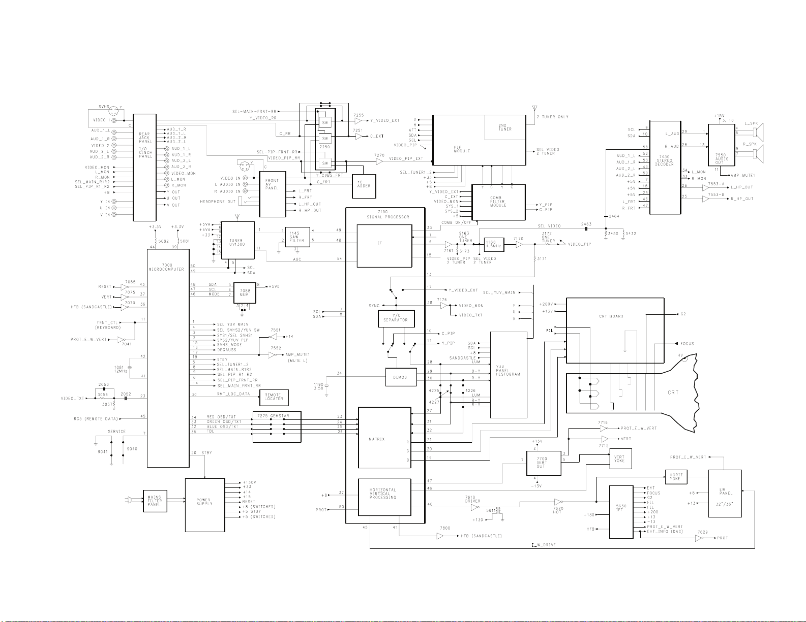
FIGURE 1 - OVERALL BLOCK DIAGRAM
page 2

Video2 as the signal source for
the outputs Y_Video_RR or
Video_PIP_RR. The SVHS input is
connected to the Video1 input.
The Y_Video_RR output of the Rear
Jack can either be composite video
from Video1 or Video 2. If the
selected Video1 input is from the
SVHS Jack, this is a luminance
signal. The Y_Video_RR is fed to
switching IC 7250, which selects
between Y_Video_RR or Y-CVBS_FRT
from the Side Jack panel. If the
input to the Side Jack panel is
from an SVHS source and this
source is selected by the user as
the PIP window, the YC is fed to
a YC adder. IC 7250 then selects
between the output of the YC adder
or the Video_PIP_RR source from
the Rear Jack panel. This
Composite signal is then buffered
by transistor 7270 and becomes
Video_PIP_EXT. This Composite
video is fed to the PIP module
where it is used as the source for
the PIP window. Selected
Composite video for the main
picture from 7250 is buffered by
transistor 7255. It becomes
Y_Video_ext and is then fed to the
Comb Filter panel and Pin 17 of IC
7150 Signal Processor. Chroma
C_RR from the Rear Jack panel's
SVHS jack is fed to 7250, which
selects between C_RR and C_FRT.
This signal is then buffered by
transistor 7255 becoming C_ext
before being fed to the Comb
Filter module. Video_PIP_RR from
the Rear Jack panel is also fed to
7250, which selects between
Video_PIP_RR or the output of the
YC adder. This signal is then
buffered by transistor 7270 and
becomes Video_PIP_ext and is fed
to the PIP module.
Composite video from 7150 Pin 6 is
buffer by transistor 7161. In the
one Tuner PIP or in the non-PIP
version, the video signal is
passed through jumper 9163. In
the two Tuner version, video is
passed through resistor 3173 to
the Video PIP input of the PIP
module. The PIP module selects
either the Video from IC 7150, or
from the second Tuner located on
the PIP module. The second Tuner
on the PIP module has its own IF
circuit. The SEL_Video in the
two-tuner version is then fed back
to the input of the 4.5 MHz trap
1167. SEL_Video is fed to the
Stereo decoding circuit for audio
processing. The signal is
buffered again by transistor 7170
before being passed to Pin 13 of
7150. In the single tuner
version, video is passed through
resistor 3172 to the Video_ PIP
input of the PIP module if this
source is selected for the PIP
window. The switch inside 7150
selects between the output of 7170
or Y_Video_ext for either the
single or two tuner versions. The
Internal/External switch of IC
7150 is controlled by the
Microcomputer via the I2C bus.
Selected video from IC 7150 on Pin
38 is buffered by transistor 7176
where it is sent to the
Input/Output (I/O) panel, the Comb
filter, and the Video Text input
of the Microcomputer. The I/O
panel has an external jack for
video output. The Comb filter
separates the video into Y
(Luminance) and C (Chroma)
signals. If the SVHS input is
selected the Y signal is fed to
the Comb filter via the
Y_Video_ext line and the C signal
is fed to the Comb filter on the
C_EXT line. The Comb On/Off line
page 3

from Pin 33 of 7150 switches the
Comb Filter between VIDEO_MON and
the SVHS input. In the PIP
versions, the Y and C signals are
sent to the PIP module. The PIP
circuit selects as the main
picture the YC signals from the
Comb filter. The YC signals from
the PIP module are then looped
through the Comb filter module to
Pins 11 and 10 of IC 7150. In
the non-PIP version, the Y and C
signals are sent to pins 11 and 10
of IC 7150 from the Comb filter.
The Chroma signal on Pin 10 is fed
to an internal Demodulator inside
7150. B-Y and R-Y signals
developed by the Demodulator and
output on Pins 29 and 30. The Y
or Luminance signal on Pin 11 is
looped through 7150 to Pin 28. In
sets with the YUV panel, Y, B-Y,
and R-Y are fed to the YUV panel.
The YUV panel then selects between
the output of 7150 or the YUV
signal from the Rear Jack panel.
The Y, B-Y, and R-Y signals from
the YUV panel are fed to Pins 27,
31, and 32 of IC 7150. The YUV
panel is a Histogram circuit,
which processes the Luminance to
set the black bias level. In sets
without the YUV panel, the Y, R-Y,
and B-Y signals are fed through
jumpers 4225, 4226, and 4227.
Red, Green, and Blue On-Screen
display signals from the
Microcomputer IC 7000 Pins 34, 33,
and 32 are fed to the Signal
Processor 7150 Pins 23, 24, and
25. Fast blanking from IC 7000
Pin 35 is fed to IC 7150, Pin 26.
The On-Screen signals are applied
to the Red, Blue, and Green
signals developed in the signal
processor matrix. Brightness,
Picture, Sharpness, Color, and
Tint control voltages are
developed within IC 7150 from the
Tuning System Microcomputer, IC
7000, via the I2C bus. The Red,
Green, and Blue signals developed
by the signal processor 7150 from
Pins 21, 20, and 19 are applied to
the CRT board. On the CRT board,
these signals are amplified before
being applied to the CRT.
The Drive and Cutoff controls for
the CRT set-up are controlled
within IC 7150 and are set by the
Microcomputer IC 7000 via the I2C
bus. Adjustments are performed
with the set in the Service Test
Mode. Always use the procedures
given in the Service Manual for
setting up the CRT circuits (White
Balance). The Drive controls are
adjusted for proper mixing of the
Luminance and Chrominance signals.
The Cutoff Controls provide
adjustment of the bias level for
the CRT cutoff values.
Horizontal and Vertical signals
are developed within IC 7150.
Adjustments for Horizontal
Centering, Vertical Centering,
AFT, and Vertical Height are done
with the Remote Transmitter via
the Service Test Mode. There is
no adjustment for the Horizontal
Oscillator. The Horizontal
circuit is a count down type of
system that gets its base
frequency from the 3.58MHz
circuit.
When the set is turned On, a High
is output from IC 7000 Pin 20 to
turn On the switched +8 volt
supply. The +8 volt supply
provides voltage to Pin 37 of IC
7150 to the Horizontal oscillator.
The Horizontal drive on Pin 40
page 4

drives transistor 7610.
Horizontal drive from transistor
7610 coupled through the Driver
Transformer 5611 to drive the
Horizontal Output transistor 7620.
The Horizontal Output transistor
7620 drives the IFT and Horizontal
Yoke. The IFT develops the high
voltage, focus voltage, and
filament voltage for the picture
tube. Scan derived voltages
provided by the IFT for use by the
chassis are the G2, +200, +13, and
-13 volt.
The Vertical signal output from IC
7150, Pin 47, is applied to the
vertical output IC 7700. The
vertical signal output from IC
7700 is applied to the Vertical
Yoke. Feedback from the vertical
circuit is fed to IC 7150, Pin 46.
Vertical output on Pin 3 of 7700
is buffered by transistor 7715 to
provide Vertical sync to the
Microcomputer to synchronize the
On-Screen Display and Closed
Caption.
The Stereo decoder IC 7430
performs audio selection and Sound
processing in the G7 chassis.
SEL_Video is fed to 7430 which has
built in Sound IF and decoding
circuits. IC 7430 selects between
internally decoded audio or from
AUD_1, AUD_2, or FRT. Left and
Right monitor audio is output on
Pins 34 and 33. This signal is
fed to the Rear Jack panel. Main
Audio is output on Pins 28 and 29
and fed to the Audio amplifier
7550 before being applied to the
speakers. Headphone audio is
output on pins 25 and 26 and is
amplified by 7553 before being
applied to the Headphone jack.
The PROT_E_W_VERT line monitors
three points to shut down the set
in case of a problem. Transistor
7716 monitors the Vertical output
circuit for failure. The IFT
circuit is monitored for
overvoltage. A circuit on the EW
panel monitors for a failure of
horizontal sweep. A failure at
any one of the three points will
place a High on the PROT_E_W_VERT
line turning On transistor 7041
causing Pin 11 of Microcomputer
7000 to go Low, turning the set
Off. In the case of an
Overcurrent condition in the IFT
circuit, the PROT line which
monitors the EHT_INFO (DAG) line
will go High. This voltage is
applied to Pin 50 of the Signal
Processor 7150. If this voltage
goes above 3.9 volts, 7150 will
detect the increase. This
information will be communicated
to the Microcomputer IC 7000
through the I2C bus. The
Microcomputer will then shut the
set Off.
G7 CHASSIS POWER SUPPLY BLOCK
(Figure 2)
When the 120Vac source is connected to the G7 chassis, approximately 160Vdc is developed by the
bridge rectifier circuit. The 160
volts dc goes through transformer
5912 to the Switch Regulator
Driver IC 3917. The Start voltage
for the switching mode power
supply is taken from the neutral
leg of the input ac.
The power supply includes a single
integrated circuit, operating as a
free-running switching mode power
supply. There is no separate
power supply for standby. The
page 5

FIGURE 2 - POWER SUPPLY BLOCK
power supply turns On when ac is
applied to the set. The switching
regulator IC 7902 starts switching
when the initial voltage is
applied through the Start circuit.
The switch inside IC 7902 turns On
and Off to allow current to flow
through the primary of the
transformer 5912. Energy stored
in the primary during the On-time
is delivered to the secondaries
during the Off-time. Positive
voltage from the hot secondary on
Pin 8 is rectified to provide
operating voltage for the
switching regulator. The
secondary 130 volt supply is the
reference voltage for the supply.
This voltage is sampled by the
Voltage Control Feedback IC 7904.
This drives the Opto-isolator
7950, which provides feedback to
IC 7902. The feedback controls
the On time of the switch inside
IC 7902.
The voltages needed to operate the
television are developed from the
secondaries of transformer 5912.
When the set is turned On, the Low
on the Standby (STBY) line turns
Off transistor 7909 to switch the
8 volt regulator switch IC 7908 On
to provide the +8 volt supply to
the set. The regulator switch IC
7907 provides Reset to the
Microcomputer, a +5 volt standby,
and a switched +5 volt supply when
the scan derived +13 volts is
applied to the IC.
page 6

FIGURE 3 - G7 POWER SUPPLY
page 7

G7 SWITCH MODE POWER SUPPLY
(Figure 3)
Startup voltage for 7902 is taken
from the neutral side of the ac
line and fed to Pin 4 through
resistor 3917. When Capacitor
2912 charges to 14.5 volts, the
oscillator inside 7902 turns On
switching the FET inside the IC
On. Voltage from Pin 8 of
transformer 5912 is rectified by
6908 to develop the operating
voltage for the IC. The 130 volt
supply is the reference supply for
the IC. The 130 volt supply drives
the feedback IC 7904 which drives
the feedback optoisolator 7950.
This causes changes in the
reference voltage on Pin 1 of 7902
to regulate the 130 volt supply.
The Power supply produces a 130
volt, 33 volt, 14 volt, and 5 volt
standby voltage when power is
applied to the set. When the set
is turned On, the On/Standby line
goes Low turning transistor 7909
Off, turning 7908 On to produce
the 8 volt source. The Low will
also turn 7955 Off. The 5V_STBY
voltage is then applied to Pin 3
of 7907 through resistors 3951 and
3980. The 5 volt regulator inside
7907 will then be switched On to
output the 5 volt source on Pin 6.
G7 HORIZONTAL OUTPUT BLOCK
(Figure 4)
The +8 volt source turns the
Horizontal Oscillator section
inside 7150 On to produce horizontal drive on Pin 40. Vertical
drive on Pin 47 drives the
Vertical output IC 7700. The
output of the Vertical Output IC
on Pin 3 drives is buffered by
FIGURE 4 - HORIZONTAL AND VERTICAL BLOCK
page 8

transistor 7715. This signal is
fed to the Microprocessor to synchronize the On Screen Display.
Vertical drive also keeps
transistor 7716 turned On to keep
the PROT_E_W_VERT line low. If
Vertical drive is lost, this turns
transistor 7716 Off, causing the
PROT_E_W_VERT line to go High
which will turn the set Off.
G7 HORIZONTAL OUTPUT CIRCUIT
(Figure 5)
Horizontal drive is fed to
transistor 7610 which drives the
Horizontal Output transistor 7620.
The Horizontal output circuit
produces High Voltage, Focus
NOTES:
Voltage, 200 volts, and G1 Voltage
to drive the CRT. A +13 volt and
a -13 volt supply is developed to
drive the Vertical output circuit.
The DAG voltage from Pin 10 of the
IFT is fed to the signal processor
to make changes in the Picture
level. This maintains the CRT at
a constant brightness level to
compensate for changes in Beam
Current. Transistor 7629 monitors
the DAG voltage to shut the set
down in the case of excessive Beam
Current. Excessive Beam current
would cause the DAG voltage to
become negative turning 7629 On.
This would cause the High Beam
Protect line to go High.
page 9

FIGURE 5 - HORIZONTAL OUTPUT CIRCUIT
page 10

G7 EAST - WEST CORRECTION CIRCUIT
(Figure 6)
East West Drive is fed to the gate
of 7680 on the East-West
correction panel to perform
linearity correction. The negative
horizontal pulses on the source
leg of 7680 keeps transistor 7658
turned Off. Transistor 7659 turns
On through resistor 3658. If the
Horizontal Output circuit should
fail, a dc voltage will develop on
the source of 7680. This will
turn transistor 7658 On, turning
transistor 7659 Off. The
PROT_E_W-VERT line will then go
High, which will shut the
Horizontal drive Off.
FIGURE 6 - EAST WEST CORRECTION CIRCUIT
G7 MICROPROCESSOR CIRCUIT (Figure
7)
The Microprocessor communicates
with the set via the control lines
and the SDA and SCL lines.
Vertical and Horizontal sync is
fed to the IC on Pins 37 and 36.
A High on the PROT_W_W_VERT line
will cause transistor 7041 to turn
On. This will cause Pin 11 of
the IC to go Low turning the set
Off.
Service Default Mode (SDM)
The Service Default Mode is used
to display Errors that have been
detected by the Microprocessor
during the operation of the set.
This is useful to the service
technician to determine what
circuit areas an intermittent
problem may have occurred. To
enter the Service Default Mode,
enter 0-6-2-5-9-6-Menu on the
remote control. To display the
Error Codes, press the Status
button on the remote. The Error
Codes will be hidden if the Status
button is pressed again. Up to
six Error Codes will be displayed.
The List of Error Codes is shown
on page 18 of the service manual.
Some of them are listed below:
0 =No Error
1 =X-ray protection, E/W
page 11
FIGURE 7 - MICROPROCESSOR CIRCUIT
page 12

protection, and/or Vertical
protection active
2 =High beam current protection
active
3 =Reserved
4 =+5V protection active
5 =Signal Processor (IC 7150)
register corrupted
To perform customer adjustments
while in this mode, press the Menu
button. The text "SDM" will
continue to be displayed in the
upper right hand corner of the
screen while adjustments are made.
To exit the Service Default Mode
and erase the Error Codes, turn
the unit Off using the power
button on the remote control.
Customer Service Mode
The Customer Service Mode (CSM)
allows the customer to retrieve
Error Data from a set that has a
working display. The customer is
instructed by phone to enter CSM
and read off the display that
appears. During this mode,
Parental lockout mode is defeated.
To enter the Customer Service
Mode, press and hold the Mute
button on the remote and the
Channel Up button on the set for
four seconds. To exit this mode,
press the power button on the
Remote or the front of the set.
Service Alignment Mode (SAM)
been On in hexadecimal format.
The next set of characters
(A80US1-2.1) displays the software
identification, country, and
software version. The characters
in the upper right hand corner of
the screen "SAM" shows that the
set is in the Service Alignment
Mode. The next line displays any
errors which may have occurred in
the set. The "SDM" mode is used
to erase the error codes. The
next line displays the OPT codes
which are the Feature Bits for the
chassis version being used. The
Feature Bits are changed in the
Options selection of the menu.
There are four selections in this
menu which are Reload Default,
Erase Buffer, Options, and
Alignments. Use the cursor up and
down buttons on the remote to
highlight the selection. Use the
cursor right button to select the
highlighted selection. Pressing
the Menu button on the Remote will
allow customer settings to be
made. The "SAM" will continue to
be displayed in the upper right
hand corner of the screen. Press
the Menu button again to return to
the alignment menu.
The "OPTIONS" selection in the
menu will allow changes to be made
in the Option Bits or Bytes. Refer
to the service manual for correct
Options of the chassis being
serviced.
Service alignments are performed
in the Service Alignment Mode. To
enter the Service Alignment Mode,
press 0-6-2-5-9-6-Status on the
Remote Control. The first set of
characters (00E6 for example) is a
Run Timer. The Run Timer displays
the number of hours the set has
The Alignment selection in the
Menu has a sub menu with four
selections. They are GEOMETRY,
WHITE TONE, TUNER, and BTSC SND.
White Tone settings are used to
set the white balance and CRT
drives. The Tuner settings are
used to set the AFT and AGC.
page 13

The Geometry selection in the menu
has eleven selections in its sub
menu. Use the cursor up-down keys
on the Remote to highlight the
desired selection. Use the cursor
right-left keys to change the
value of the selection.
NOTES:
To save the changes, turn the set
Off using the power button on the
Remote Control. To ensure that
the new settings will be read by
the Microcomputer, remove ac power
from the set for a few seconds.
page 14

START
DOES THE SET
TURN ON
DOES THE SET
SHUT DOWN
AFTER TURN ON
IS A PICTURE
PRESENT
IS COLOR
PRESENT
IS AUDIO
PRESENT
YES NO YES YES
IS 130 VOLTS
PRESENT ON 6913
CATHODE
MEASURE THE
RESISTANCE OF THE
130 VOLT LINE TO
GROUND
IS THE
RESISTANCE >4K
NO
CHECK FOR SHORTED
7620
NO
IS APPROX 140-160
VOLTS PRESENT ON
PIN 3 OF 7902
YES
CHECK FUSE 1900
AND BRIDGE 6903
NO
IS THE DRIVE ON PIN 3
OF 7902 PULSING ON
AND OFF
YES
CHECK DIODE 6908
AND RESISTOR 3959
YES
IS PIN 4 OF 7902 >
16 VOLTS
CHECK RESISTOR
3917 AND BRIDGE
6903
NO
NO YES
REPLACE 7902
DOES THE BASE OF 7909
GO LOW WHEN THE
POWER BUTTON IS
PRESSED
DOES PIN 2 OF
7908 GO TO 8V
IS PIN 1 OF 7904 >
10V
REPLACE 7908
IC7000 AND RELATED
COMPONENTS
REPLACE 7909
YES NO
YES
YES
NO
NO
YES
IS HORIZ DRIVE
PRESENT ON THE
BASE OF 7620
IS HORIZ DRIVE
PRESENT ON THE
COLLECTOR OF 7620
REPLACE 7150
TRANSISTOR 7610 OR
TRANSFORMER 5611
TRANSISTOR 7620
SET IS TURNING ON
TRY ANOTHER
SYMPTOM
YES
NO
NO
YES
NO
YES
IS HORIZONTAL
DRIVE PRESENT ON
PIN 40 OF 7150
A
YES
IC 7150 OR XTAL 1190
NO
YOUR PROBLEM IS
BEYOND THE SCOPE OF
THIS FLOWCHART
TRY CALLING FOR
TECHNICAL ASSISTANCE
YES
INSERT AUX AUDIO INTO THE
JACK PANEL AND SELECT THE
CORRECT INPUT IN THE MENU
NO
IS AUDIO
PRESENT AT THE
SPEAKERS
IC 7430
NO
IS AUDIO
PRESENT ON PINS
28&29 OF 7430
IC 7430
IS AUDIO
PRESENT ON PINS
4,6,9, AND 7 OF
7550
CHECK SPEAKERS
IS PIN 11 OF 7550
HIGH (14V) OR
LOW (0.7V)
IS 15 VOLTS
PRESENT ON PIN 3
OF 7550
IC 7550
DIODE 6918 IN THE
POWER SUPPLY
CHECK TRANSISTORS
7552 AND 7551 OR MICRO
7000
YES
NO
YES
YES
NO
LOW
HIGHNO
YES
NO
B
NO
G7
TROUBLESHOOTING
FLOW CHART
page 15

A
DOES THE SCREEN
GO BRIGHT BEFORE
THE SET SHUTS
DOWN
IS THE VOLTAGE >
3.9 VOLTS
DOES PIN 11 OF 7000 GO
LOW AFTER THE POWER
BUTTON HAS BEEN
RELEASED
NO
CHECK I2C BUS ON
PINS 49 AND 50 OF
7000
IS THE VOLTAGE ON THE
CATHODE OF 6627 > 45
VOLTS WHEN THE SET IS
TURNED ON
IS HORIZ DRIVE
PRESENT ON PIN
36 OF 7000
IS VERTICAL DRIVE
PRESENT ON PIN 37 OF
7000
IS VERTICAL DRIVE
PRESENT ON PIN 3 OF
7700
NO
YES
NOYESNO
CHECK 200 VOLT
SOURCE
RESISTOR 3643 AND
DIODE 6641
TRANSISTOR 7629,
DIODE 3628, IFT, AND
RELATED
COMPONENTS
EW CORRECTION
CIRCUIT
IC 7150
TRANSISTOR 7610 OR
7620
IFT, TUNING
CAPACITORS
YES
NO
YES
YESYES
CHECK THE DC
VOLTAGE ON PIN 50
OF 7150 WHILE
TURNING THE SET ON
NO
TRANSISTORS 7715
AND 7075
CHECK PLUS AND
MINUS 13 VOLT
SUPPLIES
7700 VERTICAL OUT
7150 SIG PROC
NO
YES
B
IS OSD (ON
SCREEN DISPLAY)
PRESENT
INSERT A COMPOSITE
VIDEO SIGNAL INTO
THE REAR JACK
PANEL AND SELECT
THAT INPUT IN THE
MENU
IS THE PICTURE
PRESENT
YES
IS > 2V p-p DRIVE
PRESENT ON PINS
19,20, AND 21 ON 7150
NO
CHECK CRT BOARD
REPLACE 7150
YES NO
C
NO
WITH THE TUNER
SELECTED, IS VIDEO
PRESENT ON PIN 6
OF 7150
YES
D
NO
IS VIDEO PRESENT
ON PIN 13 OF 7150
TRANSISTORS 7161
OR 7170
FILTER 1168
PIP MODULE IF 2
TUNER VERSION
REPLACE 7150
NO
YES
YES
page 16

D
IS 33 VOLTS
PRESENT ON PIN
12 OF THE TUNER
CHECK RESISTOR
3994 AND DIODE 6955
IS 5 VOLTS
PRESENT ON PIN 6
OF THE TUNER
SUB IF ON PIN 1 OF
1145, SAW FILTER
DOES VIDEO
APPEAR ON THE
SCREEN
SUB IF ON PIN 49 OF
7150
DOES VIDEO
APPEAR ON THE
SCREEN
REPLACE SAW FILTER
1145
REPLACE 7150
IS 5 VOLTS
PRESENT ON PIN 3
OF 7907
REPLACE 7907
CHECK 7955 AND
RELATED
COMPONENTS
NO
YES
YES
NO
NO
YES
NO
YES
NO
REPLACE TUNER
YES
C
IS VIDEO PRESENT ON THE
VIDEO_MON INPUT ON THE
COMB FILTER
IS VIDEO PRESENT
ON PIN 38 OF 7150
IS VIDEO PRESET
ON PIN 17 OF 7150
TRANSISTOR 7176
IC 7150
REAR JACK PANEL
IF Y-C PRESENT
GOING TO THE PIP
MODULE
IF PIN 33 OF 7150
APPROX 3 VOLTS
DC
NO
YES
NO
YES
NO
YES
NO
IC 7150
COMB FILTER
NO
YES
IS Y-C PRESENT
COMMING FROM THE
PIP MODULE
YES
PIP MODULE
NO
IS Y-C PRESENT
ON PINS 11 AND 10
OF 7150
COMB FILTER
YES
IS Y,R-Y, B-Y PRESENT
ON PINS 28,29, AND30
OF 7150
YES
IC 7150
NO
YES
NO
IF Y, R-Y, B-Y
PRESENT ON PINS
27, 31, AND 32 OF
7150
IC 7150
YUV PANEL
JUMPERS FOR NON
YUV SETS
NO
YES
page 17

Dear Servicers,
Welcome to the New Internet version of Service Reporter
and Technical Training Manual .
Philips Technical Training is proud to reinstate this
valuable form of update training in a more timely format.
This first issue is a test to determine the value of this
information to you as a servicer.
Please review the material presented in both the Service
Reporter and Technical Training Manual .
Please also answer the accompanying survey form and
either fax or mail it to:
Philips Technical Training
PO Box 555
Jefferson City, TN 37760
Fax # 865-475-0221
or send us your comments by e-mail at:
TECHNICAL.TRAINING@PHILIPS.COM
Sincerely,
Philips Technical Training Department

Service Reporter Survey
Please answer the following questions by selecting a rating of 1 through 5 (1 being the lowest
grade and 5 being the highest.)
1. Rate the Service Reporter article’s ability to increase your knowledge of the circuit
discussed?
1 2 3 4 5
2. How do you rate the need to ask further questions on this circuit?
1 2 3 4 5
3. Rate your ease of accessibility to articles accessible 24/7 via the Internet as is this one?
1 2 3 4 5
4. Rate how much you would like to suggest subjects for the Service Reporter on which you
need additional information?
1 2 3 4 5
5. Rate how much you like the Internet as a medium for easily accessible service information?
1 2 3 4 5
6. How do you rate the ability to access this information and print it out for your use, as you
need it?
1 2 3 4 5
7. Rate the Training Manual’s ability to increase your knowledge of the circuit discussed?
1 2 3 4 5
Thank you for your interest in and assistance to Philips Technical
Training.
Please mail or fax to: Philips Technical Training
PO Box 555
Jefferson City, TN 37760
Fax # 865-475-0221
 Loading...