

Page 1

FQ1216AME MK4
Multi-Standard Miniature Video Module
RF SOLUTIONS
Product specification
Page 2
Philips RF Solutions Product specification
•
y
Multi-Standard Miniature Video Module FQ1216AME MK4
FEATURES
• Miniaturized frontend module suitable for Notebook applications
Multi-Standard TV Systems Broadcast reception
• True 5 V device (low power dissipation)
• Full frequency range from channel E2 (48.25 MHz) to channel E69 (855.25 MHz)
• Integrated LNA for good sensitivity
• PLL controlled tuning
• Programmable PLL step size (31.25 / 50 kHz or 62.5 kHz)
• True-synchronous vision IF demodulator (PLL)
• Ultra linear FM PLL demodulator
• Demodulated video output, AF sound output, second IF sound output.
2
• I
C-bus control of tuning, address selection, AFC status information
• Complies with European regulations on radiation, signal handling and immunit
(“CENELEC 55020, 55013” )
• Low profile horizontally mounted metal 58 x 36 x 6.8 mm
3
housing
ORDERING INFORMATION
TYPE DESCRIPTION ORDER NUMBERS
FQ1216AME/R H-4
RF Pin Input / Horizontal Mounting
3139 147 21611
MARKING
The following items of information are printed on a sticker that is on the top cover of the tuner:
• Type number
• Code number
• Origin letter of factory
• Change code
• Year and week code
3139 149 11300 2 Rev h : 01.06.2005
Page 3
Philips RF Solutions Product specification
Multi-Standard Miniature Video Module FQ1216AME MK4
DESCRIPTION
The FQ1216AME family belongs to the new FM1200 MK 4 family of low profile frontends, which are designed
for Notebook TV and portable TV applications. The FQ1216AME combines the functions of Low Noise
Amplifier module, an all-band TV tuner, and a multi-standard TV IF demodulation unit for both positive and
negative modulated TV systems. The FQ1216ME is intended for CCIR L/L’ (France), B/G, I and D/K systems.
The frontends have a built-in digital (I
2
C) PLL tuning system. A DC-DC converter circuit is built-in in the
FQ1216AME to synthesize the tuning voltage required, thus making the frontend a true 5V device.
The FQ1216AME/H-4 is biased for extreme sensitivity, so care has to be taken in large signal application.
INTERMEDIATE FREQUENCIES
SYSTEM L L’ B/G D/K I
Picture carrier 38.90 33.95 38.90 38.90 38.90
Colour 34.47 38.38 34.47 34.47 34.47
Sound 1 32.40 40.40 33.40 32.40 32.90
Sound 2 - - 33.16 - NICAM 33.05 39.80 33.05 33.05 32.348
CHANNEL COVERAGE
BAND FREQUENCY (MHz)
Low band 48.25 to 158.00 MHz+
Mid band 160.00 to 442.00 MHz
High band 442.00 to 863.25 MHz
+ Can cover down to 45.75 MHz (Ch A for Ireland)
3139 149 11300 3 Rev h : 01.06.2005
Page 4

Philips RF Solutions Product specification
Multi-Standard Miniature Video Module FQ1216AME MK4
PINNING
SYMBOL PIN DESCRIPTION
N.C. 1 (AGC Monitor) Do Not Connect *
N.C. 2 (Tuning Voltage Monitor) Do Not Connect *
+5V 3 Supply Voltage Vb, Tuner section
SCL 4 I²C-Serial Clock
SDA 5 I²C-Serial Data
AS_Tuner 6 I²C-Address Select- Tuner part.
See Pg 10.
See also pg 20
NC 7 Do Not Connect (IF) *
NC 8 Do Not Connect (IF) *
nd
2
IF sound 9 Second IF sound output
CVBS 10 Composite Video Baseband Signal
AS_IF 11 I²C-Address Select- IF part
See also Pg 20
AF O/P 12 AF sound output
GROUND Mounting Tags (TH1,TH2,TH3,TH4,TH5)
* For process use only
3139 149 11300 4 Rev h : 01.06.2005
Page 5

Philips RF Solutions Product specification
Multi-Standard Miniature Video Module FQ1216AME MK4
LIMITING VALUES
Limiting values under operational conditions
The tuners are guaranteed to function properly under the following conditions.
SYMBOL PARAMETER PIN MIN. TYP. MAX. UNIT
V
AGC
AGC Voltage Monitor (not to be
1 10 M
Ω
connected)
(See Note 1)
VT Tuning Voltage Monitor (not to be
2 - - -
-
connected)
VS
V
V
SCL
SDA
Supply Voltage Vb
Ripple susceptibility (see Note 2)
20Hz - 1kHz
1kHz - 200kHz
Supply current
SCL bus input voltage 4 -0.3 5.25 V
SDA Bus input voltage
SDA Bus current (open collector)
3 4.75 5
240
5 -0.3
5.25 5 V
-1.0
5.25
2
10
280
V
mVpp
mVpp
mA
mA
AS_Tuner voltage (see Note 3) 6 5.25 V
nd
2
IF sound output
- Load impedance D.C.
A.C.
Composite Video Baseband Signal
- Load impedance D.C. (see 10.3)
(modulus) A.C.
- Load time constant
AS_IF voltage (see Note 3)
9
10
11
1.0
1.0
75
75
100
5.25
kΩ
kΩ
Ω
Ω
ns
V
AF output
- Load impedance D.C.
A.C.
12
100.0
10.0
kΩ
kΩ
Note 1 : Minimum impedance required is 10MΩ, otherwise AGC voltage is loaded down. For process only.
Note 2 : Maximum allowable Ripple voltage superimposed on the +5V supply in the frequency range from 20
Hz to 500 k H z. C riteria : for TV : ∆f<2.12 kHz or AM < 0.28%
Note 3 : For detailed information about address coding, refer to Application Information.
3139 149 11300 5 Rev h : 01.06.2005
Page 6
Philips RF Solutions Product specification
Multi-Standard Miniature Video Module FQ1216AME MK4
Environmental conditions
SYMBOL PARAMETER CONDITIONS MIN. MAX. UNIT
Non-operational Conditions
T
AMB
Ambient temperature -25 +85 °C
RH Relative humidity - 100 %
g
B
Bump acceleration 25 g - 245 m/s
gS Shock acceleration 50 g - 490 m/s
2
2
Vibration amplitude (10-55 Hz) - 0.35 mm
Operational conditions
T
AMB
Ambient temperature 0 + 70 °C
RH Relative humidity - 95 %
(1) The typical MTBF is about 20,000 hours at this operational ambient temperature.
For every 10 °C increase, the MTBF is reduced by half.
OVERALL PERFORMANCE
Conditional data
Unless otherwise specified, all electrical values for “Overall performance” apply at the following conditions.
SYMBOL PARAMETER VALUE UNIT
T
AMB
ambient temperature
RH relative humidity
25
60
±
±
5
15
o
%
C
±
0.125
5
Z
V
S
S(AE)
supply voltage (tuner and IF section)
aerial source impedance (unbalanced) 75
ZIF second IF sound output load 0.5 kΩ
V
ST
Video output load 75
AF1 sound output load 100 kΩ
V
Ω
Ω
3139 149 11300 6 Rev h : 01.06.2005
Page 7

Philips RF Solutions Product specification
Multi-Standard Miniature Video Module FQ1216AME MK4
TUNER CHARACTERISTICS
EQUIPMENT PARAMETER VALUE UNIT
DC Voltmeter
input impedance 10 MΩ
Oscilloscope input impedance
resistance
capacitance
Spectrum analyzer
input impedance 50
FET probe input impedance
resistance
capacitance
1
15
10
3.5
MΩ
pF
Ω
MΩ
pF
3139 149 11300 7 Rev h : 01.06.2005
Page 8
Philips RF Solutions Product specification
Multi-Standard Miniature Video Module FQ1216AME MK4
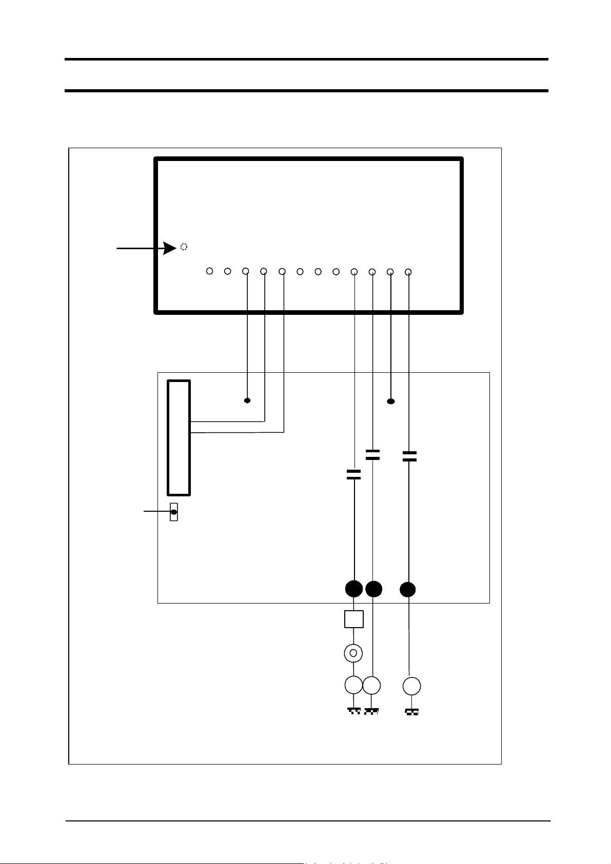
TEST DIAGRAM
The frontend characteristics are measured according to the test diagram depicted below :
TV
Signal
1 2 3 4 5 6 7 8 9 10 11 12
+ 5V
SCL
SDA
Parallel
Port
Interface
FQ1200 MK4
Eval uation boa rd
+5V
10 nF
BU2
2nd IF out
+5V
10uF
+
BU4
Video
P
33 uF
+
BU6
AF Out
SA
SA = Spectrum Analyzer
P = FET probe
DA = Di stor tion Analyzer (Zi - 100 k Ω
The minimum load impedance required at the CVBS output
75Ω (both AC and DC)
3139 149 11300 8 Rev h : 01.06.2005
)
TV
DA
Page 9

Philips RF Solutions Product specification
Multi-Standard Miniature Video Module FQ1216AME MK4
Definitions of test signals
TEST SIGNAL FREQ.
(MHz)
A0: unmodulated vision
carrier
A1: L-system signal
with video modulation
A2: B/G/D/K/I -system
signal with video
modulation
A3: L' - system signal
with video modulation.
B1: unmodulated main
sound carrier B/G/I/D/K
system as chosen
B2: AM-modulated
sound carrier L-system
B3: FM-modulated
main sound carrier
B/G/I/D/K system
respectively
B4: unmodulated 2nd
sound carrier B/G –
system
B5: unmodulated main
sound carrier L system
B6: AM modulated
sound carrier L' system
480.25 60 dB(µV)
480.25 60 dB(µV) (peak white)
480.25 60 dB(µV) (top sync.)
55.75 60 dB(µV) (peak white)
A2 +
5.5/6.0/6.5
MHz
486.75 MHz -10 dB with respect to
A2 +
5.5/6.0/6.5
MHz
A2 + 5.85
MHz
A1 + 6.5
MHz
A3 - 6.5
MHz
AMPLITUDE MODULATION
100 % (sync. level at 0%), 2T-pulse
and bar, unless otherwise indicated.
100% (rest carrier 10%), 2T-pulse
and bar, unless otherwise indicated
100% (sync. white < 6%), 2T pulse
and bar, unless otherwise indicated
-13 dB respectively wrt
A2
test signals A0 or A1
-13 dB respectively wrt
A2
-20 dB respectively wrt
A2
-10 dB wrt test signal
A1
-10 dB wrt test signal
A3
m=0.54, mod. freq. 1 kHz, unless
otherwise indicated
freq.dev.=27 kHz, mod.freq. 1kHz,
50 µs pre-emphasis, unless
otherwise indicated
M = 0.54, mod. freq. 1 kHz, unless
otherwise indicated
3139 149 11300 9 Rev h : 01.06.2005
Page 10

Philips RF Solutions Product specification
Multi-Standard Miniature Video Module FQ1216AME MK4
AERIAL INPUT CHARACTERISTICS
SYMBOL PARAMETER CONDITIONS MIN. MAX. UNIT
VSWR referred to 75 Ω at RF picture
carrier frequency
V
surge protection 5 kV
SURGE
V
ANT
antenna terminal disturbance
up to 1.75 GHz - 46
-
5
dBµV
voltage
LNA CHARACTERISTICS
Gain and Noise Figure
SYMBOL PARAMETER CONDITIONS MIN. TYP. MAX. UNIT
Gv Voltage gain 8 10 12 dB
F Noise Figure - 3.5 6 dB
GENERAL CHARACTERISTICS
SYMBOL PARAMETER CONDITIONS MIN. TYP. MAX. UNIT
fb frequency range
low band
mid band
high band
∆fb
margin
low band
mid/high band
voltage
gain
low band
mid band
high band
α
Image rejection
j
low band
mid band
high band (below 800MHz)
high band (for 800MHz
48.25
160.00
442.00
1.5
1.5
48
48
47
- wanted test signal F
at 60 dBuV
- unwanted test signal at
ant
+ 77.7) MHz
(F
ant
65
60
50
48
158.00
442.00
863.25
MHz
MHz
MHz
MHz
MHz
55
55
53
62
62
60
dB
dB
dB
dB
dB
dB
dB
and above)
IF
IF rejection
α
All bands
- wanted test signal F
- unwanted test signal A0
with frequency (F
IF,PC
ant
- 1)
.
60
dB
MHz
tlj Oscillators lock-in time Tuning speed (lock bit, CP
150 ms
= 1)
V
ESD protection at the
ESD
terminals
All terminals of each
frontend are protected
against electrostatic
discharge up to
2
KV
The products are classified
in category B (MIL-STD883C).
F
Maximum signal handling
wanted
90 100 -
dBµV
3139 149 11300 10 Rev h : 01.06.2005
Page 11

Philips RF Solutions Product specification
Multi-Standard Miniature Video Module FQ1216AME MK4
Video and audio characteristics
PARAMETER TEST SIGNAL TEST
POINT
CVBS output level
Amplitude video signal
DC level of sync. Pulse
CVBS amplitude at discrete frequencies
2 MHz
3 MHz
4.43 MHz
Sound Carriers Rejection
Specification valid for : B/G, I and D/K
mode wrt 1 MHz for :
5.5/6.0 MHz
6.5 MHz
Unweighted CVBS Signal to Noise Ratio
Specification valid for : L/L’, B/G, I, D/K
modes
Unweighted SNR
Gain limited sensitivity
(-1dB video signal)
Carrier level of test signal
PARAMETER TEST SIGNAL TEST
Audio output characteristics
Specification valid for : B/G, D/K and I
modes
AF output level (C7 = 0)
measured via LP 20 kHz filter, RMS
detector 50µs de-emphasis
for AF1 at 1 kHz (C5 = 1, C6 = 1)
Specification valid for : L/L’ mode
(C5 = 0) modulation = 54%
AF output level (C7 = 0)
Specification valid for : B/G, D/K, I
modes
THD (Total Harmonic Distortion)
Signal-to –Noise ratio
measured via LP 20 kHz filter, RMS
detector 50µs de-emphasis
for AF1 at 1 kHz (C5 = 1, C6 = 1)
Specification valid for : L/L’ mode
THD (Total Harmonic Distortion)
Signal-to –Noise ratio
measured via LP 20 kHz filter, RMS
detector for AF1 at 1 kHz
Specification valid for : B/G, D/K and I
modes (S/N = 40 dB) (C5 = 1, C6 = 1)
Audio sensitivity
Specification valid for : L/L’ mode (S/N =
38 dB)
Audio sensitivity
3139 149 11300 11 Rev h : 01.06.2005
A1
A1
A1
A1
A1
A2 + B1 + B4
A1 or A2 or A3
A2 BU4 33
A2 + B3 BU6 400 500 600 mVrms
A1 +B2 or
A3 + B6 BU6 350 450 550 mVrms
A2 + B3
A1 + B2 or
A3 + B6
A2 + B3 BU6 40
A1 + B2 or
A3 + B6
BU4
BU4
BU4
BU4
BU4
BU4
BU4 40 44 dB
POINT
BU6
BU6
BU6 45
MIN. TYP. MAX. UNIT
0.7
42
40
MIN. TYP. MAX. UNIT
-
50
-
42
1.0
0.35
0.0
- 0.5
-1.0
0.2
63
0.8
50
1.3
- 1.5
- 2.5
- 4.0
0.6
-
1.5
-
Vpp
V
dB
dB
dB
dB
dB
dBµV
%
dB
%
dB
dBµV
dBµV
Page 12
Philips RF Solutions Product specification
Multi-Standard Miniature Video Module FQ1216AME MK4
APPLICATION INFORMATION
DEMONSTRATION KIT
A demonstration kit is available for the FQ1216AME (software, Application Note and evaluation board).
Please contact your local Sales Engineer for details about the price and availability
2
I
C PROGRAMMING
For information regarding general aspects of I²C bus control see 'The I
Philips Semiconductors under the code : 9398 393 40011.
The FQ1216AME contains two I
ensure that both I
2
C devices are programmed correctly according to their addresses
2
C transceivers, one in the tuner part and one in the IF part. It is imperative to
2
C-bus and how to use it', published by
If in doubt, please refer to the demonstration software.
Tuner Part Programming (Write Mode)
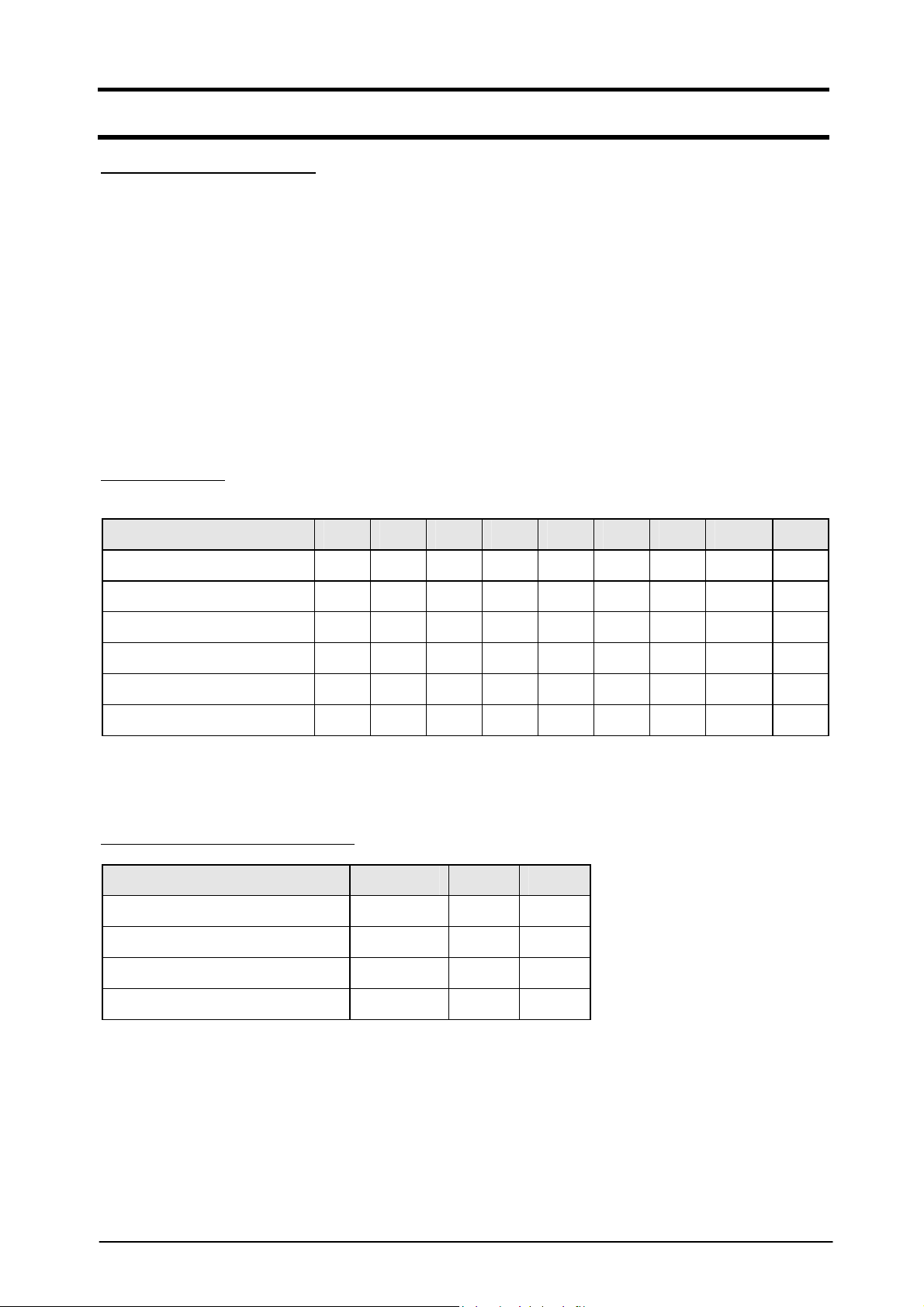
BIT ALLOCATION
(WRITE MODE , R/W = 0).
Write Data MSB bit6 bit5 bit4 bit3 bit2 bit1 LSB ACK
Address Byte ADB 1 1 0 0 0 MA1 MA0 R/W=0 A
Divider Byte 1 DB1 0 N14 N13 N12 N11 N10 N9 N8 A
Divider Byte 2 DB2 N7 N6 N5 N4 N3 N2 N1 N0 A
Control Byte CB 1 CP T2 T1 T0 RSA RSB OS A
Bandswitch Byte BB P7 P6 P5 P4 P3 P2 P1 P0 A
Auxiliary Byte AB (note *) ATC AL2 AL1 AL0 0 0 0 0 A
Note *: By default it is set to AL2=0, AL1=1, AL0=0. This sets the tuner TOP to 112 dBuV upon power-on
reset.
ADDRESS SELECTION (BYTE ADB)
Voltage at terminal 6 Address MA1 MA0
0 .......... 0.1 Vcc C0 0 0
0.2..........0.3 Vcc C2 0 1
0.4 ........ 0.6 Vcc C4 1 0
0.9 Vcc ...... 5 V C6 1 1
Note: If the AS pin is left floating, the internal biasing will automatically set the address to C2.
3139 149 11300 12 Rev h : 01.06.2005
Page 13

Philips RF Solutions Product specification
Multi-Standard Miniature Video Module FQ1216AME MK4
PROGRAMMABLE DIVIDER SETTING (BYTES DB1 AND DB2)
Divider ratio: N = F
OSC/Fss
where F
= ( FRF + FIF ) and Fss is the step-size set by RSA and RSB as described below.
OSC
N = 8192*N13 + 4096*N12 + 2048*N11 + 1024*N10 + 512*N9 + 256*N8 +
128*N7 + 64*N6 + 32*N5 + 16*N4 + 8*N3 + 4*N2 + 2*N1 + N0
Note: F
= 38.9 MHz, except for L' mode. In this case FIF = 33.95 MHz
IF
CONTROL BYTE CB
Charge Pump Setting:
CP can be set to either 0 (low current) or 1 (high current).
CP = 1, charge pump current = 280uA result s i n fa s t e st tu n i n g ( d ef au l t mode)
CP = 0 , charge pump current = 60uA results in moderate speed tuning with slightly better residual oscillator
Test Mode Setting:
T2 = 0, T1 = 0, T0 = 1 for normal operation (default)
T2 = 0, T1 = 1, T0 = 1 indicates that Byte AB will follow Byte CB instead of Byte BB for the current IIC Byte
sequence.
PLL Disabling:
OS=0 for normal operation,
OS=1 switches off the PLL tuning amplifier (PLL tuning is disabled)
Ratio Select Bits
RSA = 0, RSB = 0 gives 50 kHz step-size
RSA = 0, RSB = 1 gives 31.25 kHz step-size (for slow picture-search)
RSA = 1, RSB = 0 gives 166.7 kHz step-size
RSA = 1, RSB = 1 gives 62.5 kHz step-size (for normal picture-search)
BANDSWITCHING BYTE BB
PORTS P0 P1 P2 P3 P4 P5 P6 P7
LOW BAND 1 0 0 0 0 X X X
MID BAND 0 1 0 0 0 X X X
HIGH BAND 0 0 1 0 0 X X X
3139 149 11300 13 Rev h : 01.06.2005
Page 14

Philips RF Solutions Product specification
Multi-Standard Miniature Video Module FQ1216AME MK4
AUXILLIARY BYTE AB
The AGC Take Over Point can be set by programming the following bits AL2, AL1, AL0
IF output level,
symmetrical mode
115 dBµV
0 0 0
Remark AL2 AL1 AL0
115 dBµV
112 dBµV
109 dBµV
106 dBµV
103 dBµV
I
AGC
3.5 V
= 0
0 0 1
default mode at POR
0 1 0
Recommended for negative modulation 0 1 1
Recommended for positive modulation 1 0 0
1 0 1
External AGC . See remarks (1)
Disabled . See remarks (2)
.
.
1 1 0
1 1 1
Remarks:
1). The AGC detector is disabled. Both the sinking and sourcing current from the IC is disabled. The AGC output goes
into a high impedance state and an external AGC source can be connected in parallel and will not be influenced.
2). The AGC detector is disabled and I
AGC
= 9 µA.
It is recommended to set the internal AGC to 115 dBuV (AL2=0, AL1=0, AL0=0) .
The IF AGC should be set according to the table on Pg 17 (see bits C0 to C4).
3139 149 11300 14 Rev h : 01.06.2005
Page 15

Philips RF Solutions Product specification
Multi-Standard Miniature Video Module FQ1216AME MK4
Important:
ATC = AGC time constant.
We recommend to set the ATC = 0 for normal operation.
Tuner Part Programming (Read Mode)
BIT ALLOCATION (READ MODE R/W = 1)
MSB bit6 bit5 bit4 bit3 bit2 bit1 LSB ACK
Address Byte ADB 1 1 0 0 0 MA1 MA0 R/W=1 A
Status Byte SB POR FL 1 1 AGC A2 A1 A0 A
The following data can be read from the device through the status byte:
POR (power on reset)
end of data is detected by the PLL-IC.
FL: in lock flag (FL = 1 when the phase lock loop is in lock).
The loop must be phase-locked during at least 8 periods of the internal 7.8125 kHz reference-frequency (i.e.
1 msec) before the FL flag is internally set to 1.
: internal AGC flag. AGC=1 when internal AGC is active (level below 3V)
AGC
A2, A1, A0
: Not used.
: POR is internally set to 1 in case Vcc drops below 3V. The POR bit is reset when an
3139 149 11300 15 Rev h : 01.06.2005
Page 16
Philips RF Solutions Product specification
Multi-Standard Miniature Video Module FQ1216AME MK4
IF Part Programming (Write Mode)
The IF uses the new TDA9887 demodulation IC from Philips Semiconductors.
2
I
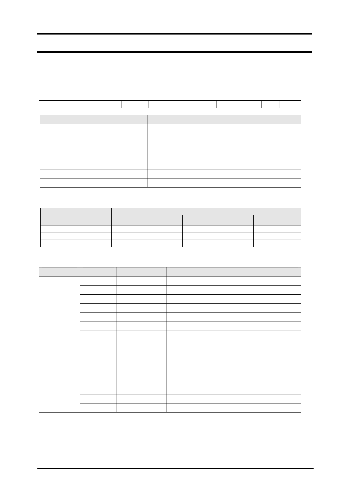
C Bus Control –format to WRITE (slave receives data)
S SLAVE ADDRESS R/W=0 A SAD A DATA A P
BIT FUNCTION
S START condition
Standard SLAVE ADDRESS 100 0011X where X is the value of R/W See Pg 20
R/W = 0 Write Mode
A acknowledge, generated by slave
SUBADDRESS (SAD) See table below
DATA Bytes B, C and E (described below)
P STOP condition
SUB ADDRESS BYTE (SAD, first byte after slave address)
DATA BYTE
FOLLOWING SAD
SWITCHING (B DATA) 0 0 X X X X 0 0
ADJUST (C DATA) 0 0 0 0 0 0 0 1
DATA (E DATA) 0 0 0 0 0 0 1 0
DESCRIPTION OF THE BITS OF THE VARIOUS DATA BYTES
DATA BYTE BIT SUBADDRESS FUNCTION
B0 SWITCHING video mode (sound trap)
B1 SWITCHING auto mute FM
B2 SWITCHING carrier mode
B DATA
C DATA
E DATA
B3 and B4 SWITCHING TV standard positive/negative modulation (B3=0)
B5 SWITCHING forced mute audio
B6 SWITCHING not used
B7 SWITCHING L/L’ Sound
Co to C4 ADJUST TOP adjustment
C5 to C6 ADJUST de-emphasis
C7 ADJUST audio gain
E0 and E1 DATA standard sound carrier
E2 to E4 DATA standard video IF
E5 DATA VIF, SIF and tuner minimum gain
E6 DATA L standard PLL gating HIGH
E7 DATA VIF-AGC
MSB LSB
D7 D6 D5 D4 D3 D2 D1 D0
3139 149 11300 16 Rev h : 01.06.2005
Page 17
Philips RF Solutions Product specification
Multi-Standard Miniature Video Module FQ1216AME MK4
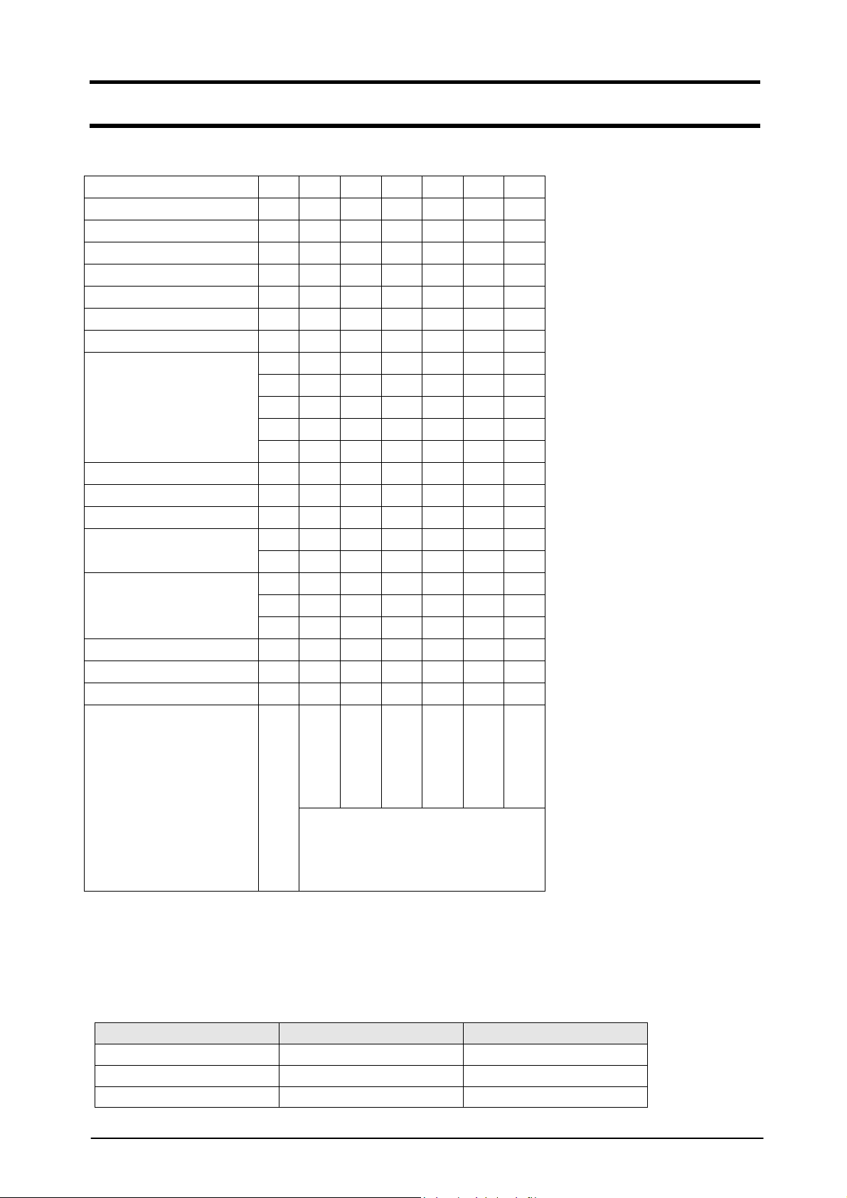
For convenience, the programming has been consolidated as a single table.
B
0
0
0
0
0
0
1
1
0
0
0
0
0
0
1
1
1
0
0
1
0
1
1
0
0
1
0
1
0
X
X
X
X
X
1
X
X
X
X
X
X
X
X
X
X
X
X
X
X
X
X
X
0
Video Trap Bypass
Auto Mute FM
Carrier Mode
FM Mode
TV Modulation
Forced Mute Audio
Not Used (OP1)
L/L’ Sound (OP2)
TOP Adjustment
See remarks *
De-Emphasis
De-Emphasis Time
Audio Gain
Sound Intercarrier
Video IF
IF Gain
L/L’ PLL Gating
VIF AGC Output
B
1
1
1
1
1
B
2
1
1
1
1
B
3
0
0
0
0
B
4
1
1
1
0
B
5
0
0
0
0
B
6
0
0
0
0
B
7
1
1
1
1
C
0
0
0
0
0
C
1
0
0
0
1
C
2
0
0
0
1
C
3
0
0
0
1
C
4
1
1
1
0
C
5
1
1
1
0
C
6
1
1
1
1
C
7
0
0
0
0
E
0
1
0
1
1
E
1
0
1
1
1
E
2
0
0
0
0
E
3
1
1
1
1
E
4
0
0
0
0
E
5
0
0
0
0
E
6
1
1
1
1
E
7
0
0
0
0
I
B/G
Bits
Description
* For optimum setting between overall picture quality and signal handling to fulfill CISPR20/EN55020
requirements, we recommend to use these settings below .
However we recommend customers have the choice to make their own setting based on their own
application. For example, for cable TV networks, the TOP has to be –4 dB or lower to prevent
intermodulation problems.
Top Setting B/G/DK/I L/L’
Low Band + 0 dB - 2 dB
Mid Band -2 dB - 2 dB
High Band + 0 dB - 2 dB
3139 149 11300 17 Rev h : 01.06.2005
D/K
TV
Systems
L
L’
Force Audio
Mute
Page 18
Philips RF Solutions Product specification
Multi-Standard Miniature Video Module FQ1216AME MK4
IF Part Programming (Read Mode)
The IF uses the new TDA9886 demodulation IC from Philips Semiconductors.
2
I
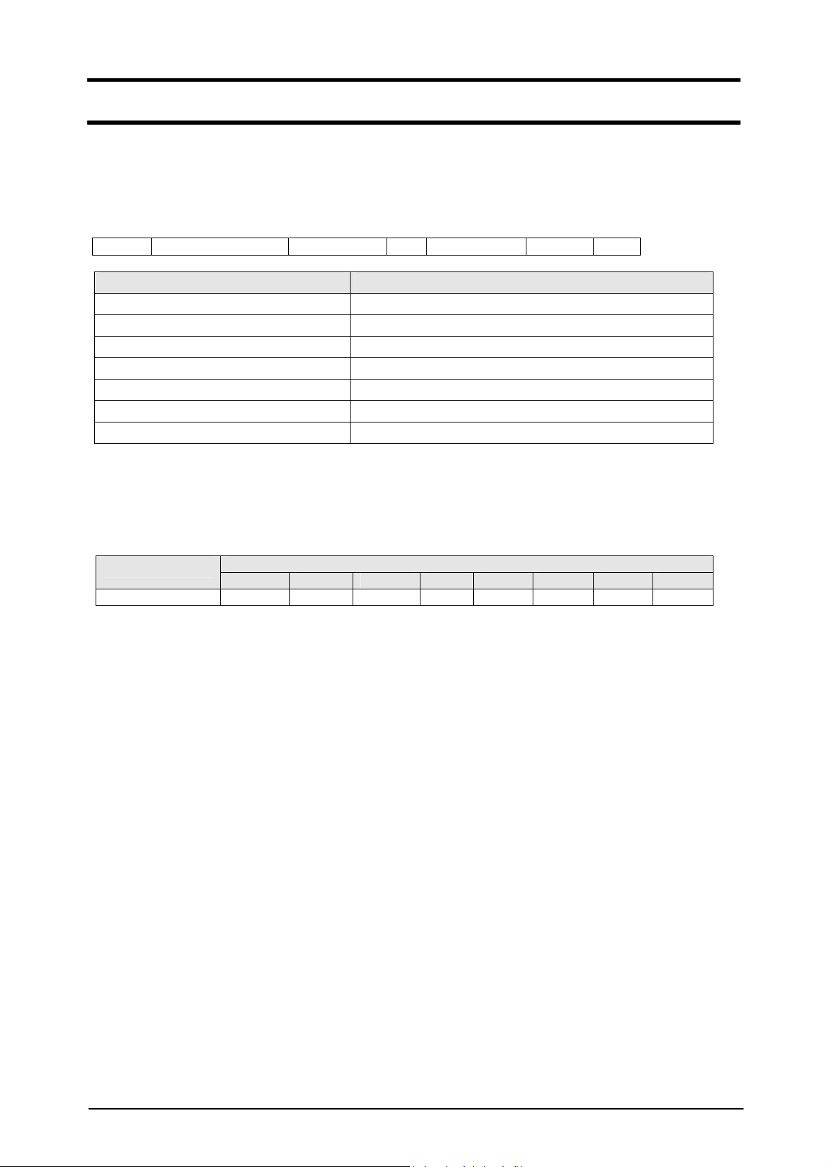
C Bus Control –format to READ (slave transmits data)
S SLAVE ADDRESS R/W=1 A DATA AN P
BIT FUNCTION
S START condition
Standard SLAVE ADDRESS 100 0011X where X is the value of R/W
R/W = 1 Read Mode
A acknowledge, generated by slave
DATA Byte D (described below)
AN acknowledge not, generated by the master
P STOP condition, generated by the master
The master generates an acknowledge when it has received the dataword READ. The master next
generates an acknowledge, then slave begins transmitting the dataword READ, and so on unt il the master
generates no acknowledge and transmits a STOP condition.
Byte D (Transmitted byte after read condition - Status Register)
FUNCTION
READ AFCWIN VIFL FMIFL AFC4 AFC3 AFC2 AFC1 PONR
PONR = 1 After power-on reset or after supply breakdown
PONR = 0 After a successful reading of the status register
FMIFL = Not used.
VIFL
= 1 Video IF level HIGH
VIFL
= 0 Video IF level LOW
MSB LSB
D7
D6 D5 D4 D3 D2 D1 D0
3139 149 11300 18 Rev h : 01.06.2005
Page 19

Philips RF Solutions Product specification
Multi-Standard Miniature Video Module FQ1216AME MK4
AFC STATUS
It is possible to monitor the AFC status via the D1-D4 bits.
Function Bits
AFC F
F
≤ F0− 187.5 kHz
VIF
F
= F0 − 162.5 kHz
VIF
F
VIF
F
= F0 − 112.5 kHz
VIF
F
= F0 − 87.5 kHz
VIF
F
= F0 − 62.5 kHz
VIF
F
VIF
F
= F0 − 12.5 kHz
VIF
F
= F0 + 12.5 kHz 1 1 1 1
VIF
F
= F0 + 37.5 kHz 1 1 1 0
VIF
F
VIF
F
= F0 + 87.5 kHz 1 1 0 0
VIF
F
= F0 + 112.5 kHz 1 0 1 1
VIF
F
= F0 + 137.5 kHz 1 0 1 0
VIF
F
= F0 + 162.5 kHz 1 0 0 1
VIF
F
≥ F0 + 187.5 kHz
VIF
vs F0 (1)
VIF
D4 D3 D2 D1
0 1 1 1
0 1 1 0
= F0 − 137.5 kHz
0 1 0 1
0 1 0 0
0 0 1 1
0 0 1 0
= F0 − 37.5 kHz
0 0 0 1
0 0 0 0
= F0 + 62.5 kHz 1 1 0 1
1 0 0 0
Note
1. F
= nominal F
0
VIF
AFCWIN = 1 F
AFCWIN = 0 F
inside AFC Window
VIF
outside AFC Window
VIF
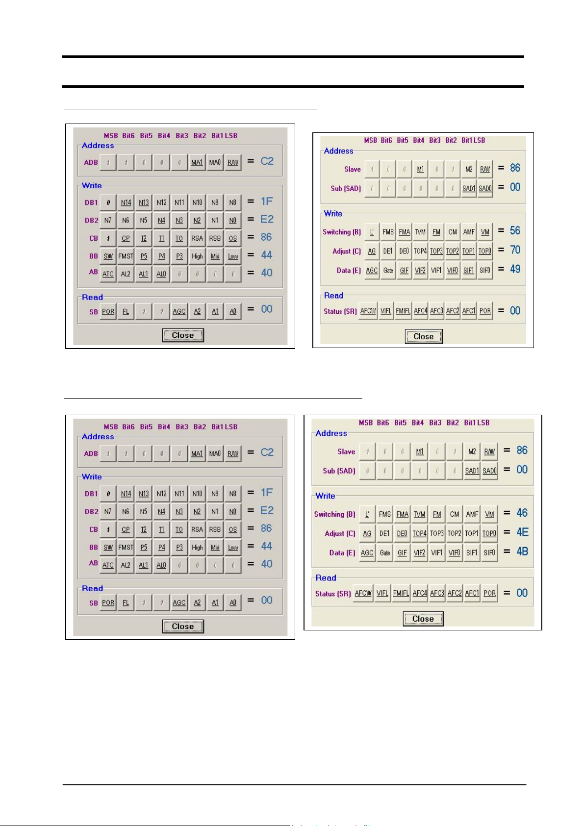
PROGRAMMING EXAMPLES
Example 1: To tune to Ch E21 (471.25 MHz) in high band
Fosc = 471.25 + 38.9 = 510.15 MHz
N = (510.15 MHz) / (62.5 kHz) = 1F E2 (Hexadecimal)
So DB1 = 1F H
and DB2 = E2 H
CB = 86H if CP is set to low or CB = C6H if CP is set to high
BB = 44H (because of high band selected)
AB = 00 H
3139 149 11300 19 Rev h : 01.06.2005
Page 20
Philips RF Solutions Product specification
Multi-Standard Miniature Video Module FQ1216AME MK4
Example 2 : To tune to a PAL B/G program at 471.25 MHz
Example 3 : To tune to a SECAM program at 471.25 MHz (L system)
Tuner I2C program
IF I2C program
Tuner I2C program
3139 149 11300 20 Rev h : 01.06.2005
IF I2C program
Page 21
Philips RF Solutions Product specification
Multi-Standard Miniature Video Module FQ1216AME MK4
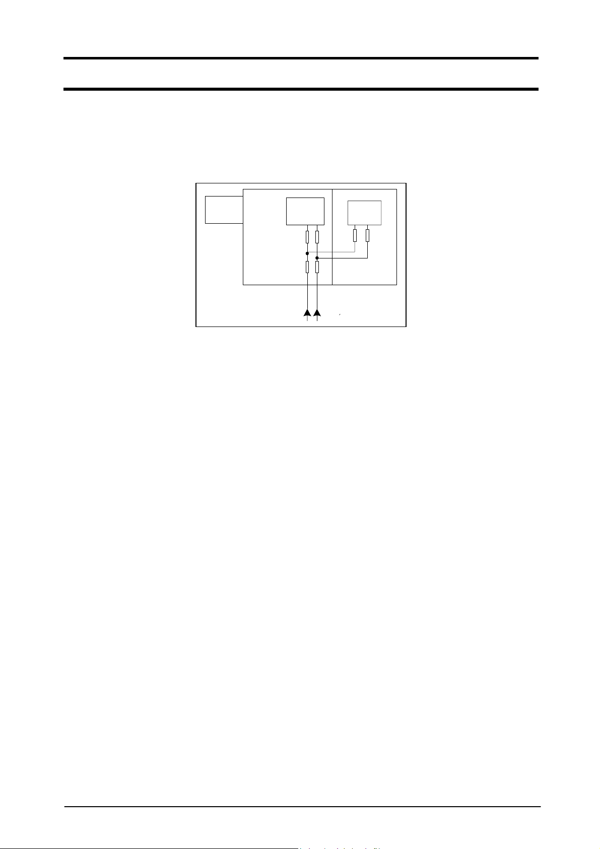
LOADING OF I2C BUS
The FQ1216AME/ H-4 contains series impedances in the SCL and SDA lines : a total of R= 220 ohms
leading to the tuner part and R= 300 ohms leading to the IF demodulation part. See the diagram below. Both
lines also have capacitive loads of C= 22 pF max. Care must be taken to ensure that the total load on the bus
does not exceed that as mentioned in the brochure "The I
2
C-bus and how to use it".
100
SDA SCL
100
120120
180 180
AUDIO EMPHASIS
The audio de-emphasis (50 us) is set by the bits C5 and C6
C5=0 de-emphasis OFF
C5=1 de-emphasis ON
C6=1 50us
C6=0 75 us
De-emphasis should be switched off in L/L’ mode since it is not required for AM sound.
CVBS LOAD / TUNING VOLTAGE SUPPLY
A video buffer is built into the frontend to enable the unit to drive a 75 Ω load directly (e.g. into the SAA711x
directly). A DC-DC converter for providing the required tuning voltage supply is already built into the
FQ1216AME.
PIP APPLICATION
By connecting a 1K resistor to ground at pin 6 and a 2K2 resistor to ground at pin 11, the tuner and IF
addresses of the second (PIP) FQ1216AME module can be set to # C0 and # 84 respectively. In this way,
the address of the main frontend remains at # C2 and # 86.
3139 149 11300 21 Rev h : 01.06.2005
Page 22
Philips RF Solutions Product specification
Multi-Standard Miniature Video Module FQ1216AME MK4
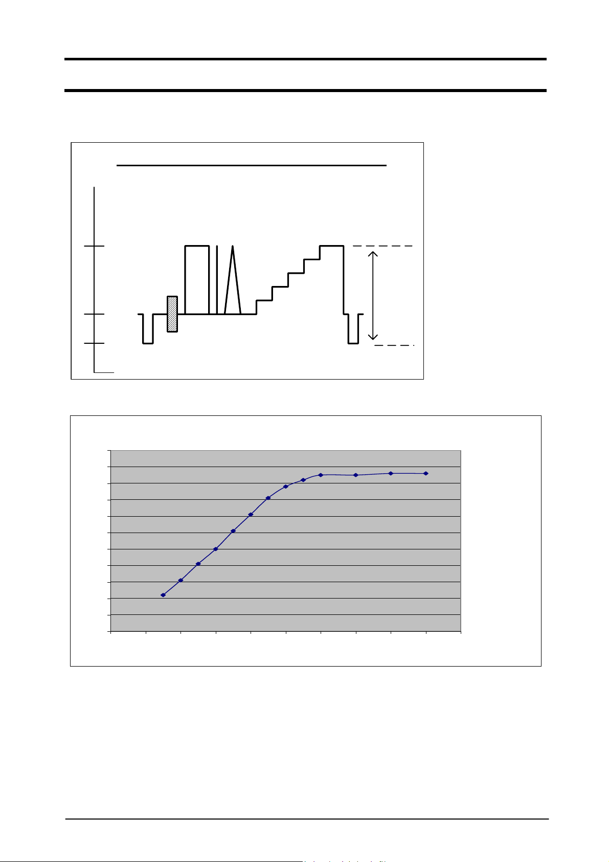
CVBS Output level
CVBS at pin 12 (into 75 ohm load)
V dc
1.35 V
1 Vpp
0.65 V
0.35 V
VIDEO SIGNAL TO NOISE RATIO
Video Signal-to-Noise Ratio (W eighted) @ C h 21
65
60
55
50
45
40
35
SNR dB
30
25
20
15
10
10 20 30 40 50 60 70 80 90 100 110
Input Level dBuV
3139 149 11300 22 Rev h : 01.06.2005
Page 23
Philips RF Solutions Product specification
Multi-Standard Miniature Video Module FQ1216AME MK4
MECHANICAL DATA
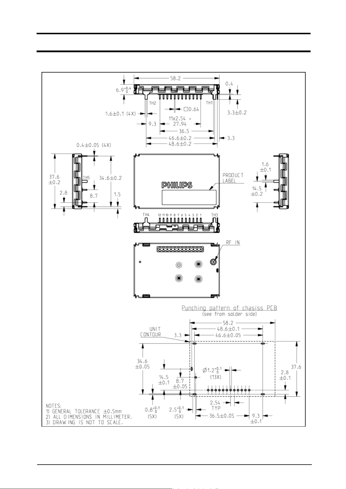
See product drawing 3139 149 0182
AERIAL CONNECTIONS
Pin connector. See product drawing 3139 149 0182
SOLDERABILITY
The solderability of pins and mounting tags when
tested initially and after 16 hour steam ageing in
accordance with “IEC 60068-2-20”, test Ta, method
1 (solder bath 235°C for 2s), results in a wetted area
of 95%. No de-wetting will occur when soldered at
260°C for 5s.
RESISTANCE TO SOLDERING HEAT
The product will not be damaged when tested in
accordance with “IEC 60068-2-20”, test Tb, ,method
1A (solder bath 260°C for 10±1 s).
MASS
Approximately 24g.
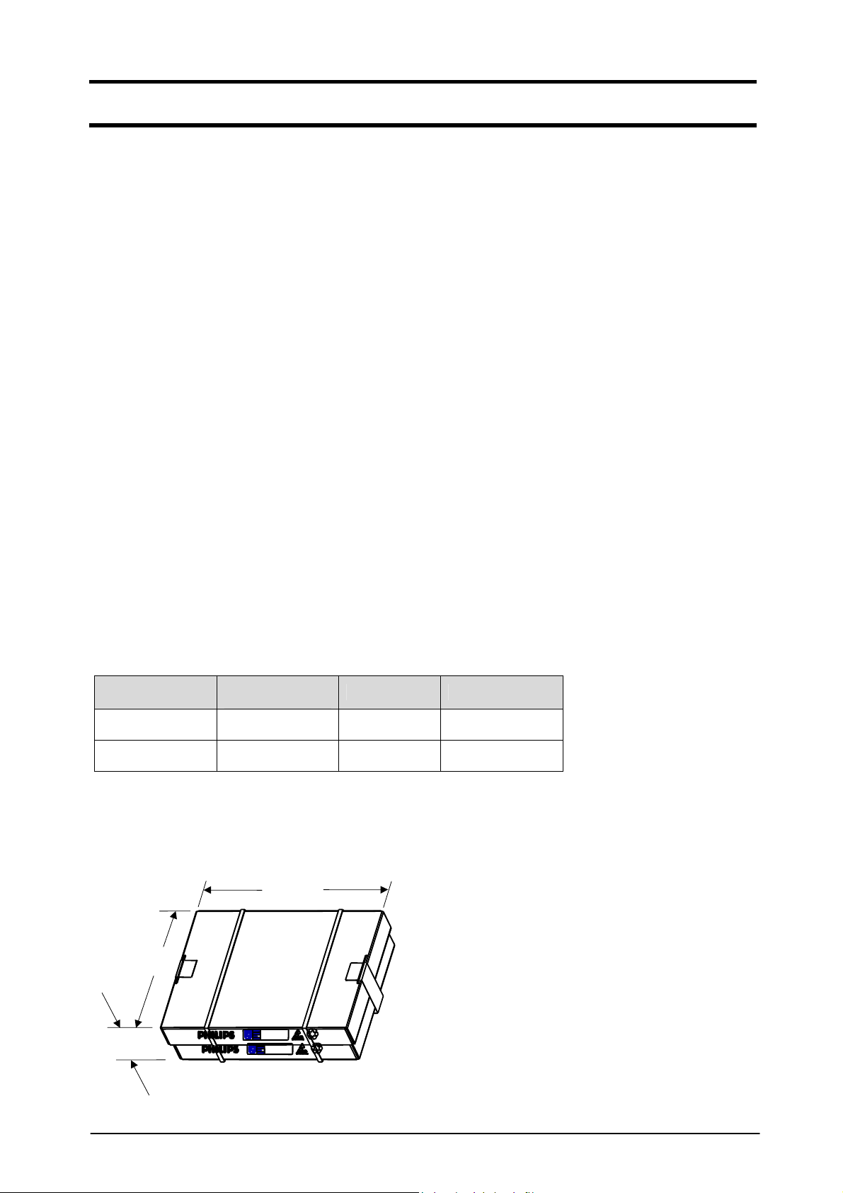
PACKAGING INFO
The products are packed in the carton box and transferred to customers by Pallet Transport.
Mounting Type
Dimension
B x w x h (cm)
No. of sets Gross Wt (Kg)
ROBUSTNESS OF PINS
The pins will not be damaged when tested in
accordance with “IEC 60068-2-21”:
• Test Ua1, tensile of 10N in axial direction
• Test Ua2, thrust of 4N in axial direction
PUNCHING PATTERN OF CHASSIS PCB
For optimum mounting of the tuner to a PCB,
the punching pattern is recommended (see
3139 149 0182).
The tuner must be mounted without clearance
between the tuner supporting surface and the
printed circuit board (PCB). When mounted in
this way, the tuner must be soldered to the
PCB. This can be achieved by pressing the
unit vertically onto the PCB during soldering.
Carton 46x3.4x5.6 90 2.76
Pallet 120x105x105 9000 298
Carton Boxes are made of Corrugated Fibreboard which are free of environmentally banned substances.
Example of Carton Box:
b
w
h
3139 149 11300 23 Rev h : 01.06.2005
Page 24
Philips RF Solutions Product specification
Multi-Standard Miniature Video Module FQ1216AME MK4
See product drawing 3139 149 0182 – Page 1 (dated on 04-09-01)
3139 149 11300 24 Rev h : 01.06.2005
Page 25

Philips RF Solutions Product specification
Multi-Standard Miniature Video Module FQ1216AME MK4
Document revision history
Rev # Date Approved by Remarks
a
a
a 04-01-15 Toh Kong Lim
b 04-03-09 Toh Kong Lim
c 04-04-28 Toh Kong Lim
d 04-06-30 Toh Kong Lim
e 04-09-16 Toh Kong Lim
f 05-04-11 Toh Kong Lim
g 05-04-26 Toh Kong Lim
h 05-06-01 Toh Kong Lim
03-03-18
03-07-03
Draft - Create new by Toh Kong Lim
Draft - Updated by Toh Kong Lim;
changes in pg 13 and 16 (Swiching to the narrowband
AGC)
Trigger by Soh Kim Leng/Toh Kong Lim;
Pg 17 – updating L/L’ Sound (OP2) – B7 table
Pg 24 – updating mechanical drawing
Trigger by Soh Kim Leng
pg 24 : Shift position of product label to cover the new
opening (refer to ECO 00699).
Trigger by Soh KL;
pg 24 : add 1x mounting tag TH5 and change top-cover
openings
Trigger by Cho Hui Ming;
Pg 10 : Voltage gain update Min/Typ/Max. and
Image rejection – High band (below 800MHz) Min. 50,
high band (for 800MHz and above) Min 48.
Trigger by Soh KL;
Updating mechanical drawing
Trigger by Toh KL;
Updating Front page;
Pg 4 : add TH5 to table
Pg 26 : Update RF Solutions Sales Offices
Triggered by Toh KL:
Updating TOP setting on Pg 17 and programming
examples on Pg 20.
Product Specification – Updated by Toh KL:
Recommend internal AGC setting to 115 dBµV on pg 14.
and IF TOP setting on Pg 17
3139 149 11300 25 Rev h : 01.06.2005
Page 26
Philips RF Solutions Product specification
Multi-Standard Miniature Video Module FQ1216AME MK4
DEFINITIONS
Data sheet status
Objective specification This data sheet contains target or goal specifications for product development.
Preliminary specification This data sheet contains preliminary data; supplementary data may be p ublished later.
Product specification This data sheet contains final product specification.
Application Information
Where application information is given, it is advisory and does not form part of the specification
LIFE SUPPORT APPLICATIONS
These products are not designed for use in life support appliances, devices, or systems where malfunction
of these products can reasonably be expected to result in personal injury. Philips customers using or
selling these products for use in such applications do so at their own risk and agree to fully indemnify
Philips for any damages resulting from such improper use or sale.
PURCHASE OF PHILIPS I
2
C COMPONENTS
Purchase of Philips I2C components conveys a license under the Philips I2C patent to use
the components in the I
This specification can be ordered using the code 9398 393 40011.
2
C systems to the I2C specification defined by Philips.
RF Solutions Sales Offices
Internet
© Philips Electronics N.V. 2005.
All rights are reserved. Reproduction in whole or in part is prohibited without the prior written consent of the copyright
owner. The information presented in this document does n ot form part of any quotation or contract, is believed to be
accurate and reliable and may be changed without notice. No liability will be accepted by the publisher for any
consequence of its use. Publication thereof does not c onvey nor imply any lic ense under patent- or ot her industrial or
intellectual property rights.
3139 149 11300 26 Rev h : 01.06.2005
: www.rfsolutions.philips.com
 Loading...