

Page 1
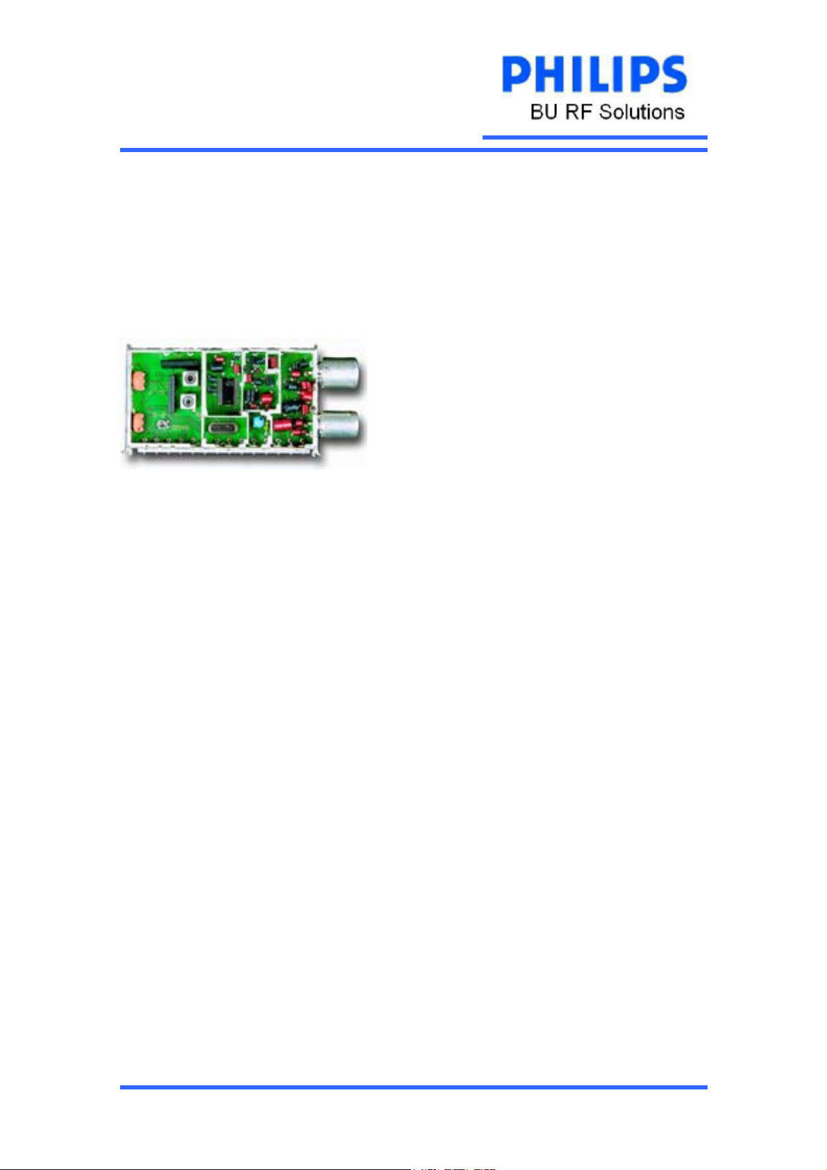
FQ1200MK3/FM1200MK3 FAMILY
Application Note
This document is believed to be correct at the time of publication. Whilst every care has been taken to
ensure its accuracy, the copyright owner accepts absolutely no liability for any losses or damages arising
from its use.
The copyright owner also reserves the right to change and update this document as and when he sees fit.
Copyright © Philips Electronics Singapore Private Limited
Business Unit RF-Solutions
Disclaimer
FQ/FM1200MK3 Application note 1
Page 2
Release Notes
Date Revision Remarks Editor
01/10/2003 1.0.0 First release Sim KP
Release Notes (Evaluation Software)
Date Revision Remarks Editor
01/08/2003 4.8.0.0 Paxton Tan
FQ/FM1200MK3 Application note 2
Page 3

Tables of contents:
1. Introduction …………………………………… 4
2. Range of Products …………………………………… 4
3. General Block Diagram …………………………………… 5
4. Pinning Information …………………………………… 5
5. Functional Description …………………………………… 6
6. Application information ………………………………… … 7
6.1 Grounding/Layout orientation ………………….. 7
6.2 Antenna socket/Cable requirement ………………….. 8
6.3 Supply requirement ………………….. 8
6.4 I
6.4.1 I
6.4.2 Tuner Programming ………………….. 9
6.4.3 IF Programming ………………….. 13
6.4.4 I
6.5 Specific Pin Connections ………………….. 24
6.5.1 Loading of I
6.5.2 FM AF-L/AF-R ………………….. 24
6.5.3 2
6.5.4 CVBS Output ………………….. 25
6.6 TV Stereo Sound System ………………….. 26
6.7 Approbation ………………….. 26
7. Appendix …………………………………… 27
7.1 Appendix A: TV Auto-tuning flow chart …………. 27
7.2 Appendix B: FM Auto-tuning flow chart …………. 28
7.3 Appendix C: FQ1236 MK3 Noise Figure …………. 29
7.4 Appendix D: Video SNR …………. 29
List of Figures:
Figure 1: General Block Diagram of FQ/FM1200MK3 ………………….. 5
Figure 2: Suggested Layout ………………….. 7
Figure 3: Suggested Supply De-coupling circuit ………………….. 8
Figure 4: I
Figure 5: I
Figure 6: AF-R/AF-L Pins ………………….. 24
Figure 7: 2
Figure 8: CVBS Output ………………….. 25
2
C Programming requirement ………………….. 9
2
C Bus Structure ………………….. 9
2
C Bus Loading ………………….. 24
nd
IF Sound Output ………………….. 25
2
C Bus Structure ………………….. 9
2
C Programming Examples ………………….. 22
2
C Bus ………………….. 24
ND
Sound IF Output ………………….. 25
FQ/FM1200MK3 Application note 3
Page 4

This document serves as a guideline to maximize the performance of this module for various
applications.
1. Introduction
The FM1200Mk3 and FQ1200Mk3 are the new family of RF video modules family. The MK3
family is the small size front-ends which is designed to meet wider range of RF applications in the
areas like PC/TV Multi-Media; LCD TV; PVR and etc. It combines the functions of an all bands
tuner, and a Quasi-Split Sound (QSS) IF Demodulation unit.
The frontends have a built-in digital (I
in to synthesize the tuning voltage, thus making the frontends the true 5V device.
The FQ1200Mk3 and FM1200MK3 are complied all the requirements of FCC, CISPR, JIS, DOC
(canada) as well as CENELEC (EN55013, EN55020) with respect to input immunity and EMC.
2. Range of Products
Types TV standard / Countries
2
C) PLL tuning system. A DC-DC converter circuit is built-
Input connector/
Mounting
12 NC
FQ1216ME/I H-3 IEC/Horizontal 3139 147 18291
FQ1216ME/P H-3 Phono/Horizontal 3139 147 18771
FQ1216ME/I V-3
FQ1236/F H-3 F/Horizontal 3139 147 18351
FQ1236/P H-3 Phono/Horizontal 3139 147 18761
FQ1236/F V-3
FQ1286/F H-3 F/Horizontal 3139 147 18981
FQ1286/P H-3
FM1216ME/I H-3
FM1236/F H-3
FM1286/F H-3
Note : option for active loop-through; passive loop-through, LNA are available.
CCIR B/G, I, D/K, L/L’
Western Europe, East Asia, China,
OIRT countries, France, UK, HK,
NZ, Australia
M/N
USA, Canada, Latin America,
Taiwan, S Korea, Philippines
M/N
Japan
CCIR B/G, I, D/K, L/L’ & FM
Western Europe, East Asia, China,
OIRT countries, UK, France, HK,
NZ, Australia
M/N and FM radio
USA, Canada, Latin America,
Taiwan, S Korea, Philippines
M/N and FM radio
Japan
IEC/Vertical 3139 147 19151
F/Vertical 3139 147 19521
Phono/Horizontal 3139 147 20171
IEC/Horizontal 3139 147 18201
F/Horizontal 3139 147 18261
F/Horizontal 3139 147 19011
FQ/FM1200MK3 Application note 4
Page 5
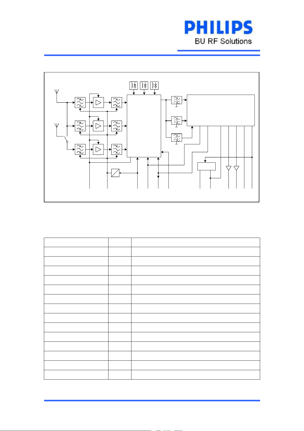
3. General Block Diagram
TV
antenna
33V
5V
RF AGC
do not connect
Figure 1, General Block Diagram of FQ/FM1200MK3
Vtuning
do not connect
4. Pinning Information
Symbol Pin Description
RF
AGC
Oscillators
MOPLL
+5V
SCL SDA
I2C BUS
IF
* 10.7MHz Filter
Address
Select
Video
SAW Filter
Sound
SAW Filter
IF Demodulator IC
Stereo Decoder
*AF-R
*FM Radio
TDA988X
*FM Radio
*AF-L/
AS IF
CVBS AF2nd IF
+5V
N.C 1 Do not Connected (agc Monitor)
N.C 2 Do not Connected (tuning voltage monitor)
+5V 3 Supply Voltage Vb, Tuner section
SCL 4 I2C – Serial Clock
SDA 5 I2C – Serial Data
AS 6 I2C – Address Select
- 7 Do not Connected
- 8 Do not Connected
N.C/AF-R 9 Do not Connected / FM radio Right channel
IF AS /AF-L 10 I2C – Address Select IF/ FM radio Left channel
2nd Sound IF 11 Second Sound IF output (buffered output)
CVBS 12 Video (buffered output)
+5V IF 13 Supply Voltage, IF section
AF/MPX 14 AF/MPX TV sound output
FQ/FM1200MK3 Application note 5
Page 6

5. Functional Description
The FQ/FM1200 Mk3 frontend consists of a 3-band tuner that can tune to all channels between
48 and 863 MHz covers all types of TV systems, and an IF system using QSS demodulation
concept, designed on a single double-sided Printed Circuit Board. The whole assembly is
mounted in a steel folded frame for good EMC performance.
TV Tuner
The tuner section is equipped with 3 tuned RF high-gain MOSFET stages in the input section,
ensuring low noise and good inter-modulation performance. The gain control voltages of the
MOSFETs are by the wideband AGC voltages generates from the tuner IC when it detects the
level of the IF output. The AGC take-over point and the time constant are selectable by the I
bus. A band-pass filter, suitably narrow with a 3dB bandwidth of 8-12 MHz, ensures good
suppression of unwanted spurious channels. The mixer-oscillator functions are based on an IC
which offers good intermodulation and suppression of oscillator harmonics. An IF amplifier
provides some gain conversion to drive the SAW filter directly in the IF section. The tuning and
bandswitching is done with a digital programmable PLL tuning system contained in the
synthesizer IC. The DC-DC converter is built around this IC to provide the required tuning
voltages, making the FQ/FM1200 Mk3 frontends the true 5V devices.
The FM radio is integrated with the TV VHF Low band tuner. When switched to FM Radio
mode, the tuner RF bandwidth is reduced to about 2.5MHz.
IF section
The IF is designed base on the Philips Semiconductor IF demodulator IC TDA9885/6/7 depend
on the versions. It is a true synchronous demodulation, alignment–free multistandard (PAL,
SECAM and NTSC) IC for positive and negative modulation via I
including AM and FM works on the principle of Quasi Split Sound (QSS) processing. For
demodulating the video IF, an extremely linear synchronous PLL demodulator is utilised. Its
offers very linear demodulation good intermodualtion, reduce harmonics, and excellent pulse
response. The IF selectivity is provided by a Video Surface-Acoustics Wave (SAW) filter, and
split Sound SAW filter for the different TV systems. The PLL demodulator is fitted with an
Automatic Frequency Tuning (AFT) detector which allows for fine tuning of the picture carrier
to the nominal IF.
FM Radio, a separate 10.7MHz IF bandpass filter is connected to the FM input of the TDA9887
IF IC at pin 13. FM radio demodulation is controlled via I
to TDA7040 Stereo decoder IC where the L and R audio channels are decoded.
The 2nd IF sound signal at pin 11 is intended for Stereo/NICAM sound decoding. The 2nd IF
sound output is buffered and it can be connected directly to the NICAM/Multi system DSP
sound IC.
2
C-bus. The sound IF
2
C. The FM MPX sound is connected
2
C
FQ/FM1200MK3 Application note 6
Page 7
6. Application information
6.1 Grounding / Layout Orientation
The FQ1200 MK3 and FM1200 MK3 modules are housed in a metal enclosure that has two
function: firstly, preventing the Local Oscillator signals from radiating into the environment and
secondly, preventing unwanted RF signals from entering the module and disturbing the wanted
signals to be received.
The second function is most critical, since the PC environment is an extremely “polluted” one
with a plethora of clock and control signals. The fundamental and harmonic frequencies of
many digital signals extend below and beyond the frequency range in use for TV broadcasts.
Due to their very high levels, they can easily leak into the frontend and create interference with
the wanted TV signals.
To prevent this from happening, it is recommended not to place the digital radiators, especially
the VGA and video decoder ICs in close proximity to the frontend. And the crystals that
associated to Video decoder and sound decoder should not place near to the frontend. Care must
also be exercised regarding the length of PWB tracks going to the pins of the frontend. At
certain frequencies, long PWB tracks act like micro-strip lines, presenting a low impedance to
the frontend terminals, so that the internal decoupling capacitors on the terminals are no longer
effective.
It is essential that a separate analogue ground system be established for the frontend. A ground
plane under the frontend is recommended. All tracks carrying digital signals should not be run
underneath the frontend. Connections between the analogue and digital ground should be made
only via RF chokes. In addition, the analogue ground plane should be in contact with the chassis
ground via the slot bracket screw contacts.
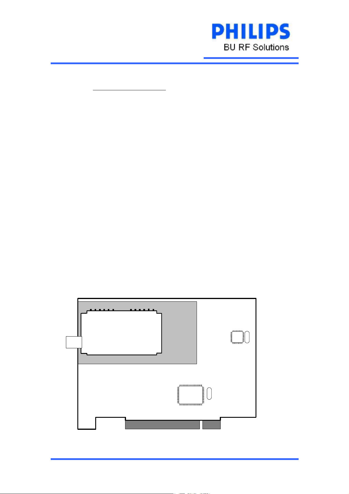
The most optimum layout configuration is obtained when the antenna connector of the frontend
protrudes from the back of the PC chassis when the TV card is installed. This ensures that the
RF signal connection is made directly to the frontend. The use of a extra antenna adapter or
cable will degrade the quality of the RF signal. Also it is very critical that the frontend is not
located next to any digital device in an adjacent card that radiates a lot of spurious signals into
the environment. See Fig 1
Figure 2,. Suggested card Layout
Crystal
Stereo
deocder
Video decoder
Crystal
FQ/FM1200MK3 Application note 7
Page 8
6.2 Antenna socket / Cable requirement
To prevent excessive loss of signal and picking up of spurious signals under sub-optimal
conditions, the antenna cable must be of good quality. A recommended type is the RG-59BU
with a characteristic impedance of 75 ohm (preferable double shielded). This has a specified
maximum loss of 4.6 dB at 1GHz.
The antenna connector must be properly crimped or soldered to the cable. F and IEC connector
are recommended as their characteristics are closer to 75 ohm than the RCA (frequently called
standard phono) type. This will ensure an optimum matching to the antenna wall outlet and the
frontend.
6.3 Supply requirements
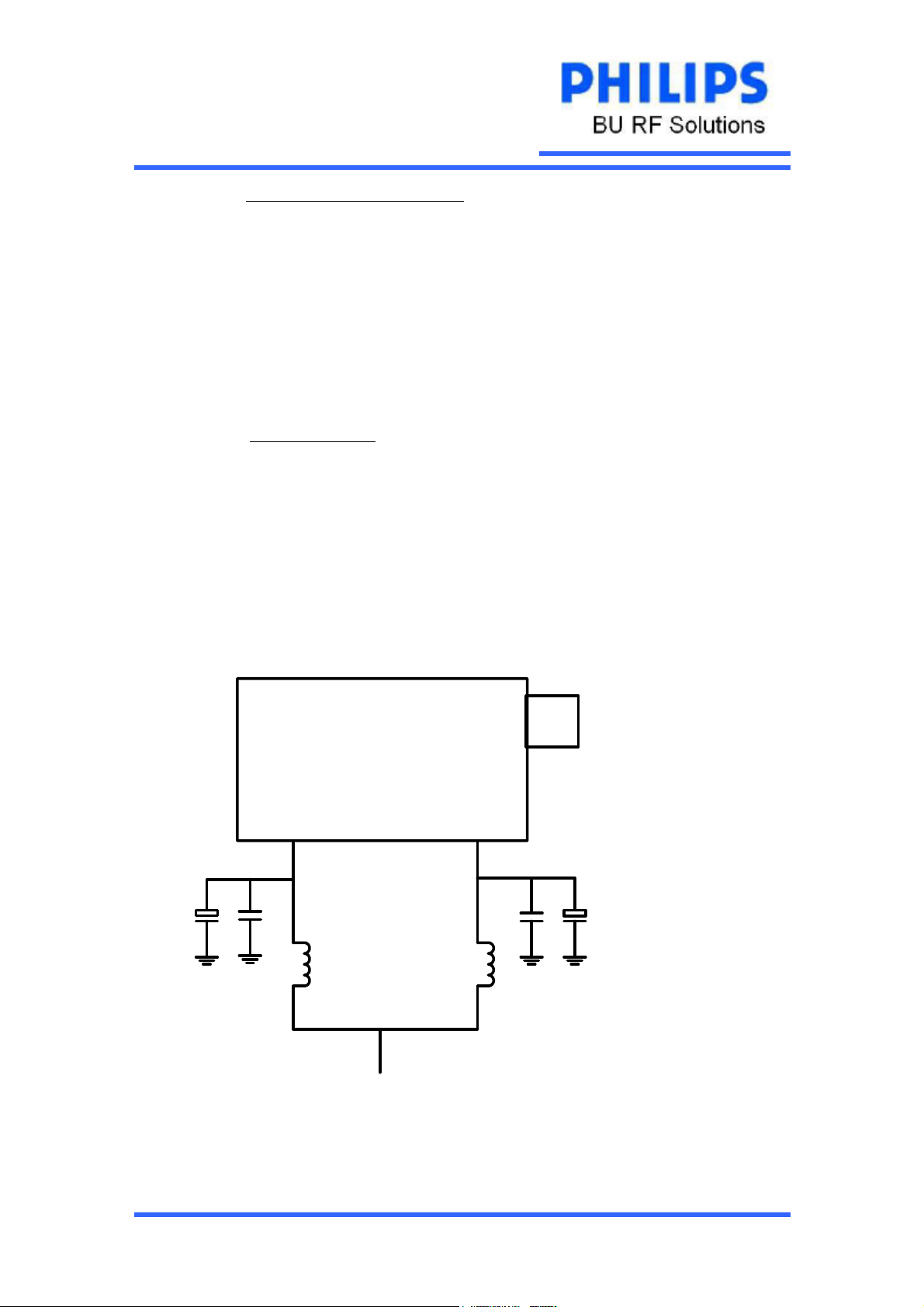
The FQ/FM1200 Mk3 is the true 5V device. For optimum protection against unwanted pick-up,
it is recommended that a series choke of 10 nH and a large Elcap (100 uF) be placed at pins3
and 13. See figure 2. The maximum allowable ripple is 5 mVpp in the frequency range 20 Hz to
100 kHz and 10 mVpp from 100 kHz to 500 kHz. . Ideally the frontend should be powered by a
separate voltage regulator which is capable of sourcing at least 310mA (150mA for tuner part
and 160 mA for the IF part). The frontend works best with a nominal voltage of +5V. It should
be verified that the supply voltage at the pins 3 and 13 is at least 4.75V.
It is imperative that good grounding techniques be employed in order to prevent conducted
radiation from the digital decoder IC through the analogue/digital grounding.
100uF 100uF
0.1uF
5V Input5V Input
Pin 3Pin 13
0.1uF
10uH
10uH
Figure 3, Suggested Supply de-coupling circuit
+5V
FQ/FM1200MK3 Application note 8
Page 9
6.4 I2C Bus Programming
For information regarding general aspects of I²C bus control see
published by Philips Semiconductors under 12NC : 9398 393 40011
The next section provides programming information specific to the FQ/FMI1200 Mk3 modules.
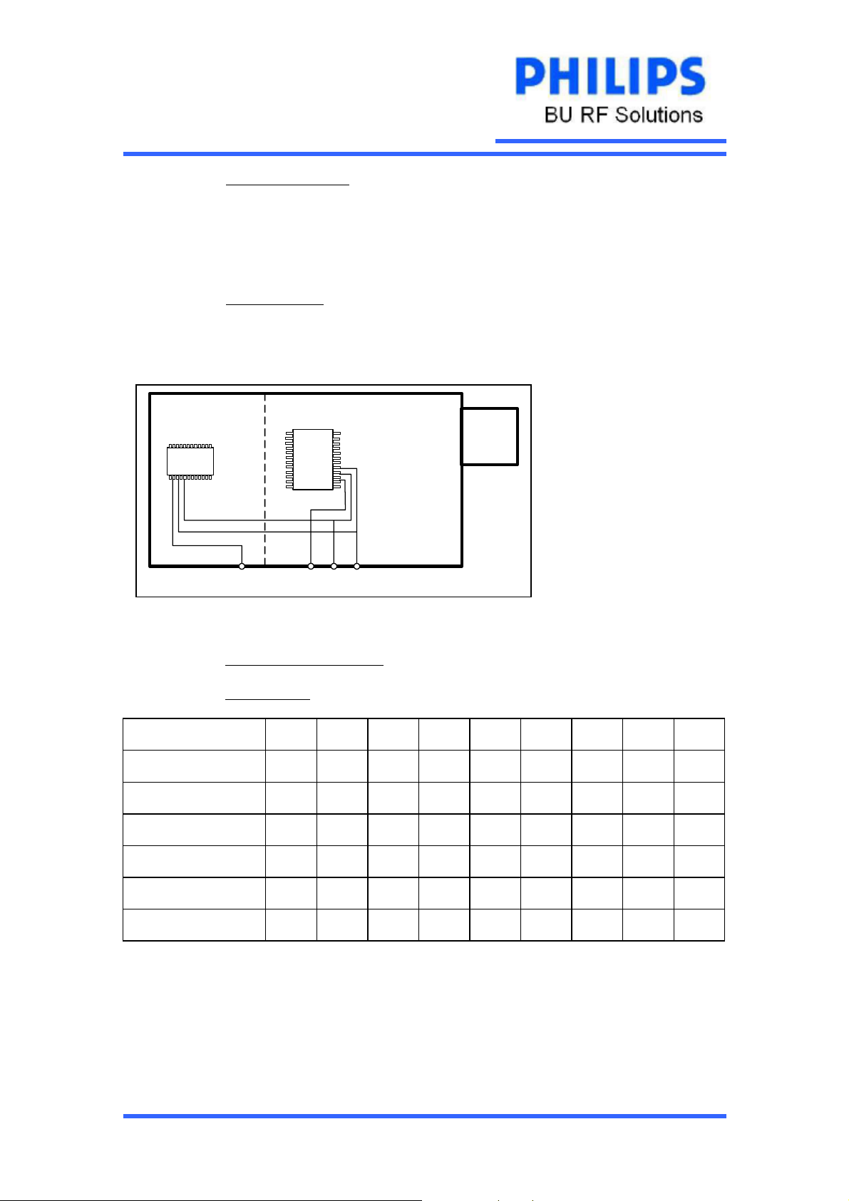
6.4.1 I
The FQ/FM1200 MK3 contains two I
section. It is imperative to ensure that both I
2
C Bus Structure
2
C transceivers, one in the tuner section and one in the IF
2
C devices are programmed correctly according to
their address.
10 6 5 4
AS IF AS
Figure 4, I2C Bus Structure
Tuner SectionIF Section
2
C Bus
I
6.4.2 Tuner Section Programming
6.4.2.1 Logic Diagram
(WRITE Mode , R/W = 0)
'The I2C-bus and how to use it',
MSB LSB ACK
Address Byte ADB 1 1 0 0 0 MA1 MA0 R/W=0 A
Divider Byte 1 DB1 0 N14 N13 N12 N11 N10 N9 N8 A
Divider Byte 2 DB2 N7 N6 N5 N4 N3 N2 N1 N0 A
Control Byte CB 1 CP T2 T1 T0 RSA RSB OS A
Bandswitch Byte BB P7 P6 P5 P4 P3 P2 P1 P0 A
Auxiliary Byte AB * ATC AL2 AL1 AL0 0 0 0 0 A
*Note : By default, it is set to AL2=0, AL1=1,ALO=0. This sets the tuner AGC TOP to 112dB
µV upon
power –on reset.
FQ/FM1200MK3 Application note 9
Page 10

6.4.2.2 Address Byte (MA1, MA0)
Voltage at Pin 6 of the tuner (AS pin) Address MA1 MA0
0 - 0.5 V C0 0 0
1.0 – 1.5 V C2 0 1
2.0 – 3.0 V C4 1 0
4.5 – 5.0 V C6 1 1
If the AS pin (pin 6 of the tuner) is left floating, or not connect to any voltage, the internal biasing will
automatically set the address to C2.
6.4.2.3 Programmable Divider Setting (Byte 1 and Byte 2)
Divider ratio: N = f
Where f
OSC
= f
RF. PC
Thus, N = 8192*N13 + 4096*N12 + 2048*N11 + 1024*N10 + 512*N9 + 256*N8 +
128*N7 + 64*N6 + 32*N5 + 16*N4 + 8*N3 + 4*N2 + 2*N1 + N0
For : FQ/FM1216ME MK3, f
FQ/FM1216ME MK3, f
FQ/FM1236MK3, f
FQ/FM1286MK3, f
and : FM radio, f
6.4.2.4 Control Byte CB
6.4.2.4.1 Charge Pump Setting:
CP can be set to either 0 (low current) or 1 (high current).
CP = 1 results in fastest tuning
CP = 0 in moderate speed tuning with slightly better residual osc FM.
For TV mode, it is recommended to set CP=1. The only exception allowed is when fine tuning
under viewing conditions, then a low current CP=0 should be selected, but returning to CP=1
immediately after completion of fine tuning.
For FM radio mode, it is recommended to set CP=0 at all times.
/ fSS
OSC
+ f
MHz and fSS = step size set by RSA and RSB
VIF
= 38.9MHz B/G, D/K, I, L mode
VIF
= 33.9MHz L’ mode
VIF
= 45.75MHz NTSC USA
VIF
= 58.75MHz NTSC Japan
VIF
= 10.7MHz
VIF
FQ/FM1200MK3 Application note 10
Page 11
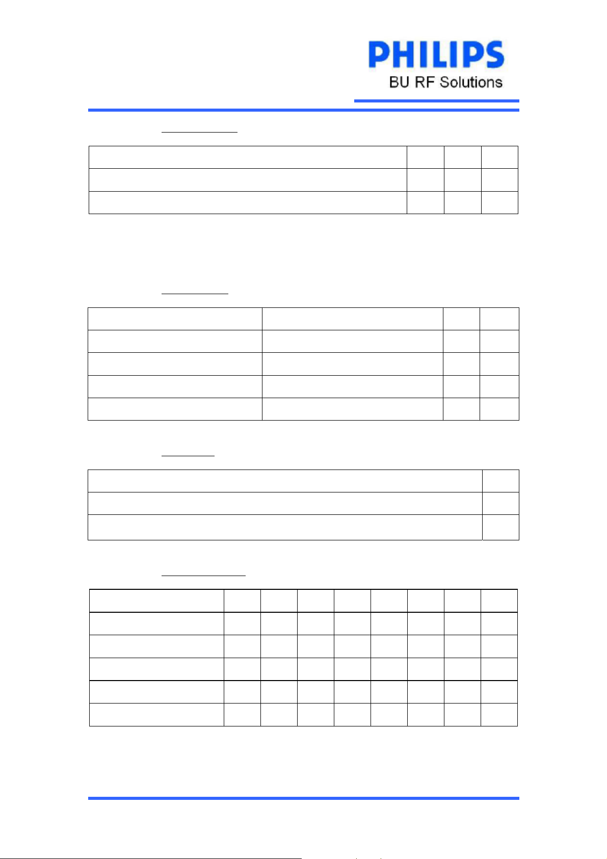
6.4.2.4.2 Test Mode Setting:
Mode T2 T1 T0
Normal operation (default) 0 0 1
Byte AB will follow byte BB (otherwise BB Byte will follow) 0 1 1
It is default to set test bits at normal operation mode. The only exception when AB byte is used, this is necessary
when at TV mode, the AGC time constant ( bit ATC ) and AGC TOP (bits AL2, AL1, AL0 ) should change to
recommended values. (refer to AB bytes)
6.4.2.4.3 Ratio Select Bits
Frequency step size (f
) RSA RSB
SS
50kHz For FM tuning 0 0
31.25kHz For slow TV tuning 0 1
166.7kHz 1 0
62.5kHz For normal TV tuning 1 1
6.4.2.4.4 PLL Disabling
OS
For normal operation 0
Disable PLL tuning
1
6.4.2.5 Bandswitch Byte CB
P7 P6 P5 P4 P3 P2 P1 P0
TV Low Band X X X 0 0 0 0 1
TV Mid Band X X X 0 0 0 1 0
TV High Band X X X 0 0 1 0 0
FM band Stereo X 0 X 1 1 0 0 1
FM Band Mono X 1 X 1 1 0 0 1
FQ/FM1200MK3 Application note 11
Page 12
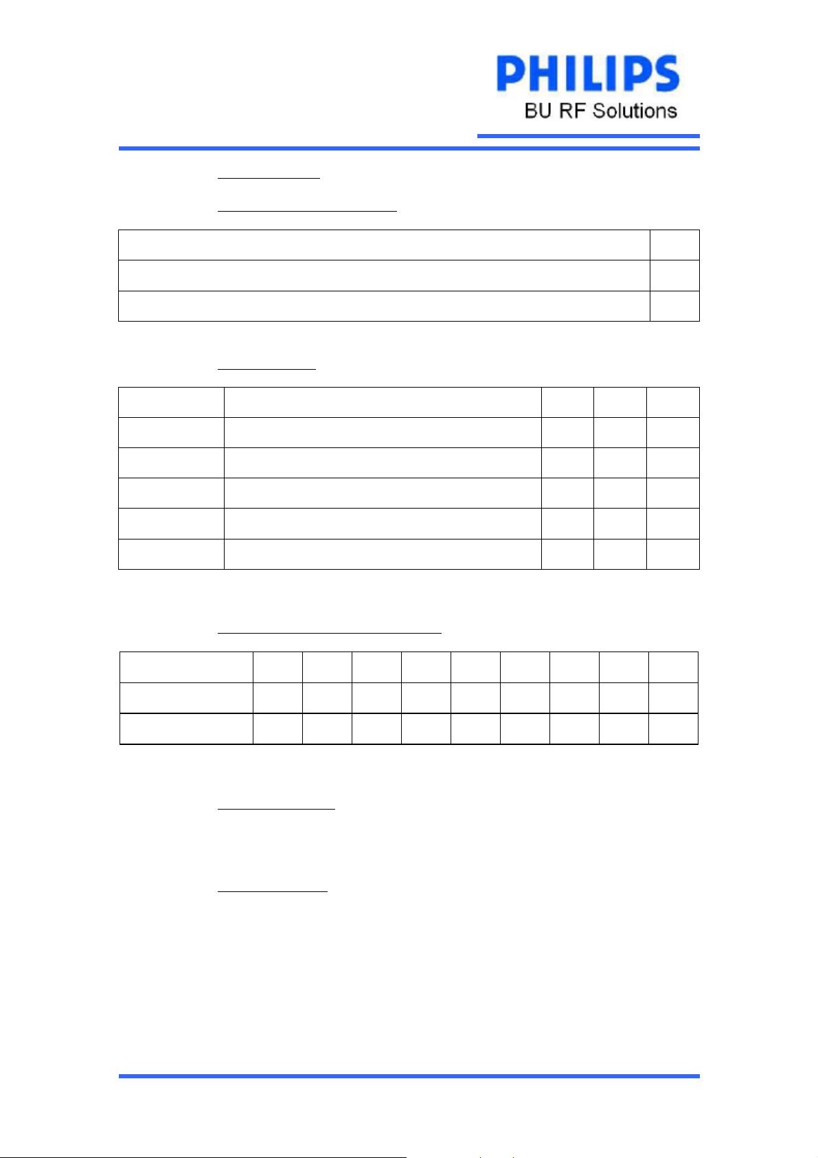
6.4.2.6 Auxiliary Byte AB
6.4.2.6.1 AGC Time Constant (ATC Byte)
ATC
AGC time constant = 2sec (recommended setting for all TV Systems and FM radio) 0
AGC time constant = 50msec (Not recommended setting) 1
6.4.2.6.2 AGC TOP Setting
IF Output Level AL2 AL1 AL0
115 dBµV 0 0 0
112 dBµV Default mode at POR 0 1 0
109 dBµV 0 1 1
106 dBµV Recommended for PAL B/G, D/K, I & NTSC & FM 1 0 0
103 dBµV Recommended for only L/L’ 1 0 1
6.4.2.7 Logic Diagram (READ MODE R/W = 1)
Address Byte ADB 1 1 0 0 0 A1 MA0 R/W=1 A
Status Byte SB POR FL 1 1 AGC A2 A1 A0 A
The following data can be read from the device through the status byte:
6.4.2.7.1 POR (power on reset)
The POR bit = 1, at power-one
6.4.2.7.2 FL (PLL Lock Flag)
FL = 1, when the phase lock loop is in lock
The loop must be phase-locked during at least 8 consecutive periods of the internal 7.8125 kHz
reference-frequency (ie. 1msec respectively) before the FL flag internally will be raised to 1.
MSB LSB ACK
:
FQ/FM1200MK3 Application note 12
Page 13
6.4.2.7.3 AGC : Internal AGC flag
AGC
Internal AGC is Non-active 0
Internal AGC is active 1
6.4.2.7.4 A2, A1, A0
Used for indicating if the FM radio signal received is in Stereo or Mono mode.
These bits do not apply to TV mode.
A2 A1 A0
FM Radio Stereo mode 1 0 0
FM Radio Mono mode 0 X X
6.4.3 IF Section Programming
6.4.3.1 Logic Diagram (WRITE Mode, R/W = 0)
2
I
C bus format to write (slave receives data)
S SLAVE ADDRESS R/W= 0 A SAD
DATA
AN P
BIT FUNCTION
S START condition, generated by the master
Standard SLAVE ADDRESS See table 1
R/W = 0 Write command, generated by the master
A Acknowledge, generated by the slave
SUBADDRESS (SAD) See table 2 and 3
DATA 8 bits data words, transmitted by the master, See table 4,5,6
AN Acknowledge not, generated by the master
P STOP condition
FQ/FM1200MK3 Application note 13
Page 14
6.4.3.2 Standard SLAVE ADDRESS
Table 1, Slave address
Value (hex) A6 A5 A4 A3 A2 A1 A0 R/W
86 1 0 0 0 0 1 1 0
84 1 0 0 0 0 1 0 0
Default address = 86 (hex), pin 10 open
Alternate address = 84 (hex), 2
ground.
6.4.3.3 SUBADDRESS (SAD)
There are 3 byte of data can be transmitted, such as B data; C data and D data. SAD is used to
point to desired data to be transmitted. If more than 1 byte of data is transmitted, then autoincrement is performed; starting from the transmitted sub-address and auto-increment of subaddress in accordance with the order of table below is performed.
Table 2, Definition of the subaddress (second byte after slave address)
Function
nd
tuner for PIP application. Pin 10 connect a 2k2 resistor to
MSB LSB
(1)
D7
D6 D5 D4 D3 D2 D1 D0
Switching (B DATA) 0 0 0 0 0 0 0 0
Adjust (C DATA) 0 0 0 0 0 0 0 1
Data (E DATA) 0 0 0 0 0 0 1 0
(1): D7 = 1 is not allowed.
Table 3, Examples for more than 1 byte of data is transmitted (auto-increment is performed)
S Slave address R/W SAD DATA DATA DATA P
00 B C E
01 C E
02 E
FQ/FM1200MK3 Application note 14
Page 15
6.4.3.4 Description of the various Data bytes
6.4.3.4.1 B Data
Table 4, Definition of B data
Bit Values Description
Remarks
L’ Sound Switch
B7
B6
B5
B4, B3
B2 = 1 QSS Mode
B1
B0 = 0 Sound trap active
6.4.3.4.2 C Data
Table 5, Definition of C data
= 1
= 0
= 1
= 0
= 1
= 0
= 00
= 10
= X1
= 1
= 0
L’ Sound
B/G, I,D/K, L ,M/N Sound
FM sensitivity setting
High sensitivity
Normal sensitivity
Force audio mute
On
Off
TV standard Modulation and radio mode
Positive modulation
Negative modulation
FM radio
Mute of FM AF outputs
Active
Inactive
Only for FM auto-tuning
L/L’
B/G,D/K,I, M/N
Recommended
Bit Values Description Remarks
Audio gain
C7
C6
C5
C4 to C0
**: Incase the for BTSC; SAP and FM radio applications, the de-emphasis must be switched OFF.
= 1
= 0
= 1
= 0
= 1
= 0
=10000
- 6dB
0dB
De-emphasis time constant
50µs
75
µs
De-emphasis
On
Off
Tuner AGC Take over point setting
Not applicable
FM Stereo only
For all TV mode
PAL B/G, D/K,I
NTSC M/N
PAL B/G, D/K, I
L/L’, NTSC M/N, FM**
Default setting
FQ/FM1200MK3 Application note 15
Page 16

6.4.3.4.3 E Data
Table 6, Definition of E data
Bit Values Description Remarks
E7
E6
E5
E4, E3, E2
E1, E0
VIF AGC Output
= 0
= 1
= 1
= 0
= 000
= 001
= 010
= 100
= 00
= 01
= 10
= 11
Off
L standard PLL gating HIGH
Gating in case of 36% positive modulation
IF gain
Minimum
Normal
Video IF Frequency
= 58.75MHz
f
VIF
f
= 45.75MHz
VIF
= 38.9MHz
f
VIF
= 33.9MHz
f
VIF
Sound carrier frequency
= 4.5MHz
f
FM
f
= 5.5MHz
FM
= 6.0MHz
f
FM
= 6.5MHz
f
FM
For all setting
For all setting
FM mode
TV mode
NTSC Japan
NTSC
B/G, D/K, I, L
L’
NTSC M/N
PAL B/G
PAL I
PAL D/K, L ,L’
FQ/FM1200MK3 Application note 16
Page 17
6.4.3.4.4 For convenience, the programming has been consolidated as a single table
6.4.3.4.4.1 TV mode FQ1216ME MK3
Sound Intercarrier
E
0
E
1
E
2
1
0
0
0
1
0
1
1
0
1
1
0
1
1
0
X
X
X
Video IF
IF Gain
L/L’ PLL Gating
VIF AGC Output
TOP Adjustment
De-Emphasis
De-Emphasis Time
Audio Gain
Video Trap Bypass
Auto Mute FM
Carrier Mode
E
3
E
4
E
5
E
6
E
7
C
0
C
1
C
2
C
3
C
4
C
5
C
6
C
7
0
B
B
1
B
2
1
0
0
1
0
0
0
1
0
1
1
1
0
0
1
1
1
0
0
1
0
0
0
1
0
1
1
1
0
0
1
1
1
0
0
1
0
0
0
1
0
1
1
1
0
0
1
1
1
0
0
1
0
0
0
1
0
1
0
1
0
0
1
1
0
1
0
1
0
0
0
1
0
1
0
1
0
0
1
1
X
X
X
X
0
X
X
X
X
X
X
X
X
X
X
X
FM Mode
TV Modulation
Forced Mute Audio
Not Used (OP1)
L/L’ Sound (OP2)
Description
B
B
B
B
3
4
5
6
7
Bits
0
1
0
0
0
B/G
0
1
0
0
0
I
0
1
0
0
0
D/K
TV
0
0
0
0
0
L
Systems
0
0
0
0
1
L’
X
X
1
X
X
Force Audio Mute
B
FQ/FM1200MK3 Application note 17
Page 18
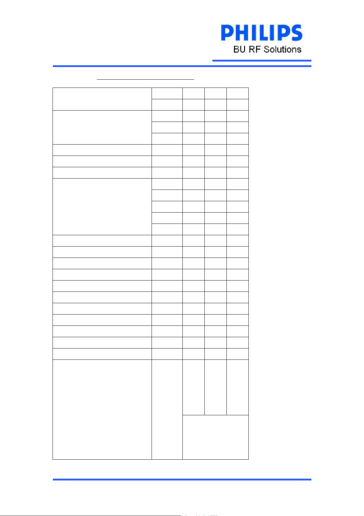
6.4.3.4.4.2 TV Mode FQ1236 MK3 / FQ1286 MK3
Sound Intercarrier
E
0
E
1
E
2
0
0
1
0
0
1
X
X
X
Video IF
IF Gain
L/L’ PLL Gating
VIF AGC Output
TOP Adjustment
De-Emphasis
De-Emphasis Time
Audio Gain
Video Trap Bypass
Auto Mute FM
Carrier Mode ***
E
3
E
4
E
5
E
6
E
7
C
0
C
1
C
2
C
3
C
4
C
5
C
6
C
7
0
B
B
1
B
2
0
0
0
1
0
0
0
0
0
1
1
0
0
0
1
1
0
0
0
1
0
0
0
0
0
1
1
0
0
0
1
0
X
X
X
X
0
X
X
X
X
X
X
X
X
X
X
X
B
B
B
B
B
3
4
5
6
7
Bits
FM Mode
TV Modulation
Forced Mute Audio
OP1 (Not used)
OP2 (Not used)
Description
0
1
0
0
X
M
0
1
0
0
X
M / Japan
TV
Systems
X
X
1
X
X
Force Audio Mute
FQ/FM1200MK3 Application note 18
Page 19
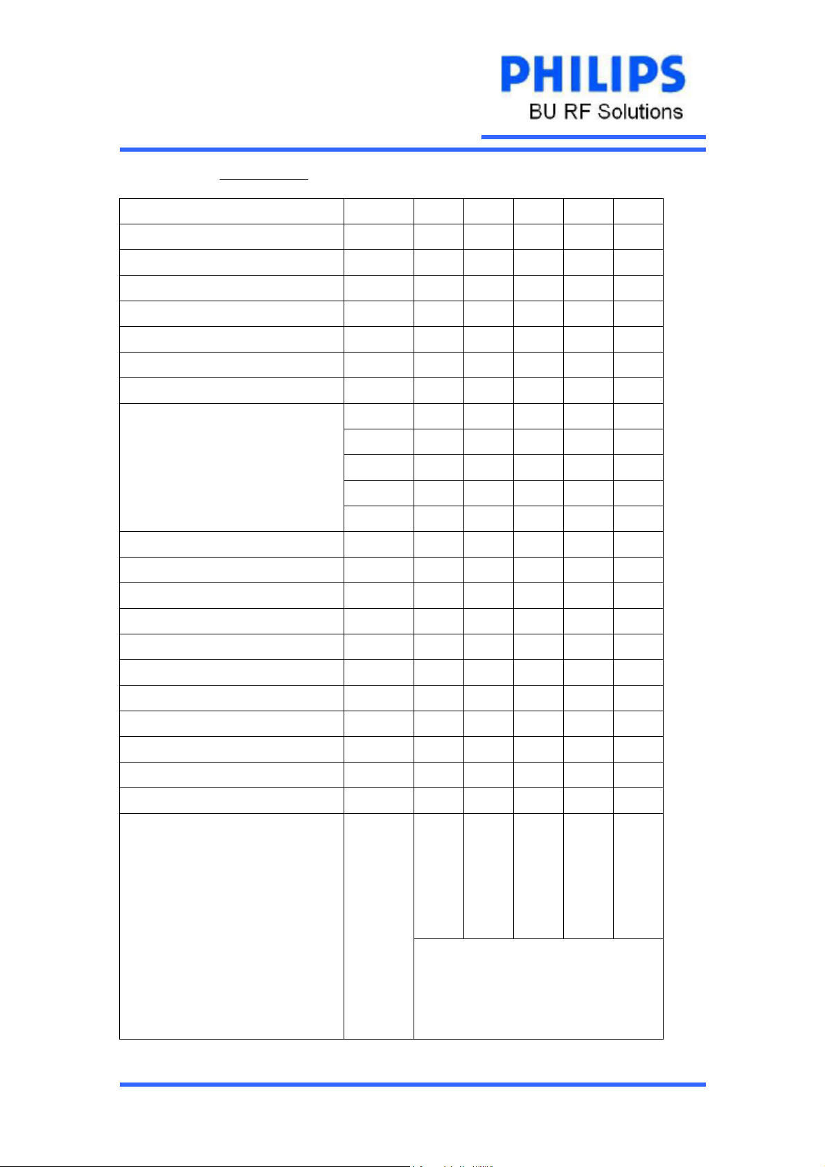
6.4.3.4.4.3 FM Radio mode
Sound Intercarrier
Video IF
IF Gain
L/L’ PLL Gating
VIF AGC Output
E
0
E
1
E
2
E
3
E
4
E
5
E
6
E
7
C
0
C
1
X
X
X
X
X
1
X
0
0
0
X
X
X
X
X
1
X
0
0
0
X
X
X
X
X
1
X
0
0
0
X
X
X
X
X
1
X
0
0
0
X
X
X
X
X
X
X
0
X
X
TOP Adjustment
De-Emphasis
De-Emphasis Time
Audio Gain
Video Trap Bypass
Auto Mute FM
Carrier Mode
FM Mode
TV Modulation
Forced Mute Audio
FM Sensitivity (OP1)
L/L’ Sound (OP2)
C
2
C
3
C
4
C
5
C
6
C
7
0
B
B
1
B
2
B
3
B
4
B
5
B
6
B
7
0
0
1
0
X
1
X
1
X
1
X
0
X
X
0
0
1
1
0
0
X
1
X
1
X
0
X
X
0
0
1
1
0
0
X
1
X
1
X
0
1
X
0
0
1
1
0
0
X
1
X
1
X
0
0
X
X
X
X
X
X
X
X
X
X
X
X
1
X
X
Stereo
Bits
Description
Mono
High Sensitivity
FM
Normal Sensitivity
Force Audio Mute
FQ/FM1200MK3 Application note 19
Page 20
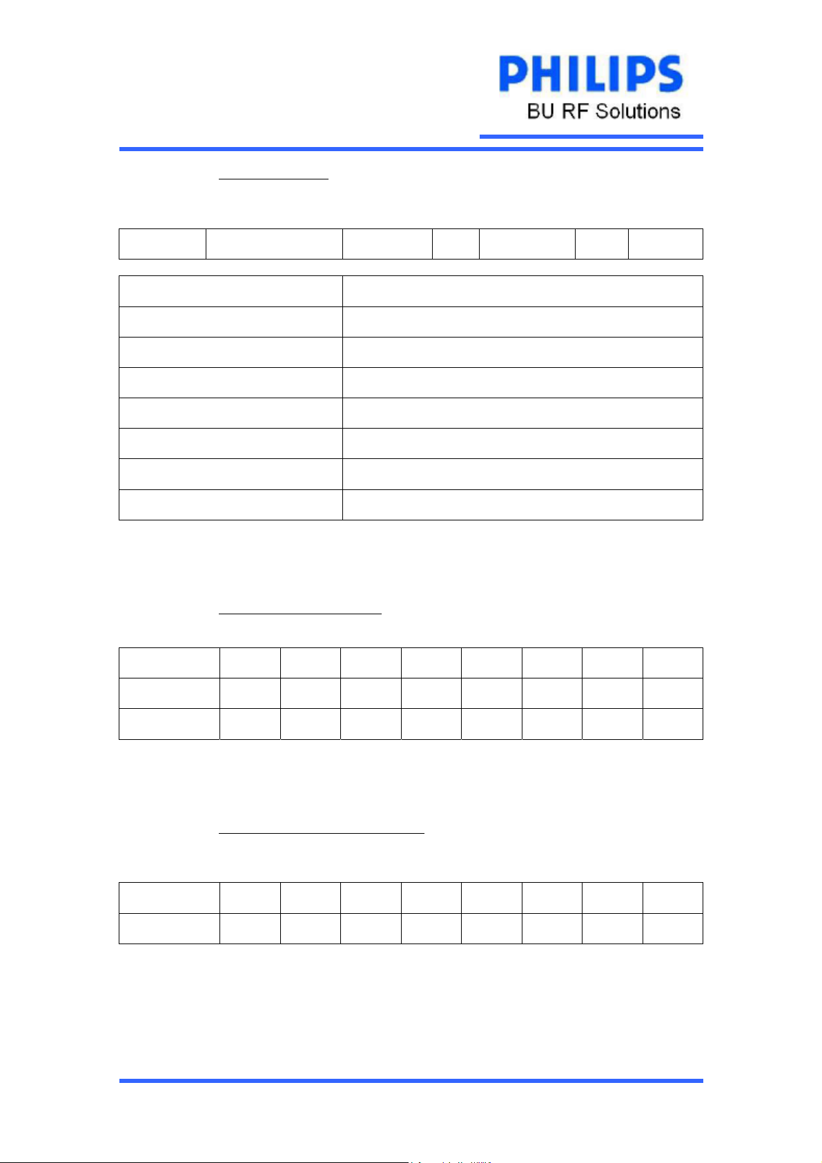
6.4.3.5 LOGIC DIAGRAM (READ MODE , R/W =1)
2
C bus format to Read (Slave transmits data)
I
S SLAVE ADDRESS R/W= 1 A DATA AN P
BIT FUNCTION
S START condition, generated by the master
Standard SLAVE ADDRESS See table 7
R/W = 1 Read command, generated by the master
A Acknowledge bit, generated by the slave
DATA 8 bit data words, transmitted by the slave, see table 8
AN Acknowledge-not bit, generated by the master
P STOP condition
The master generates an acknowledge when it has received the data word READ. The master next
generates an acknowledge, then slave begins transmitting the data word READ, and so on until the
master generates no acknowledge and transmits a STOP condition.
6.4.3.6 Standard SLAVE ADDRESS
Table 7, Slave address
Value (hex) A6 A5 A4 A3 A2 A1 A0 R/W
87 1 0 0 0 0 1 1 1
85 1 0 0 0 0 1 0 1
Default address = 86 (hex), pin 10 open
Alternate address = 84 (hex), 2
nd
tuner for PIP application. Pin 10 connect a 2k2 resistor to
ground.
6.4.3.7 Description of the various Data bytes
Definition of the transmitted byte Data D, after read condition (status register)
Function D7 D6 D5 D4 D3 D2 D1 D0
Read
AFCWin
VIFL FMIFL AFC4 AFC3 AFC2 AFC1 POR
FQ/FM1200MK3 Application note 20
Page 21
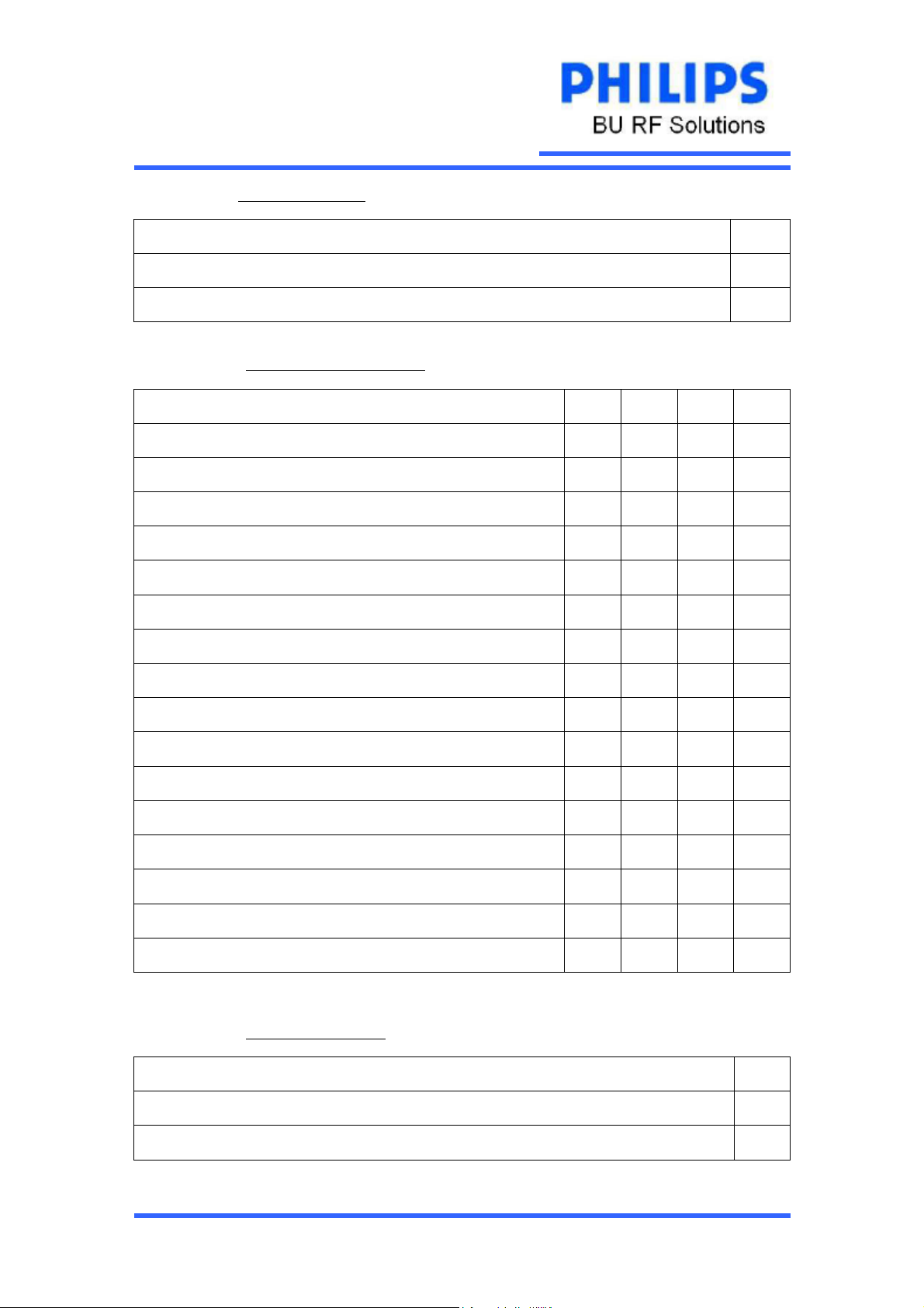
6.4.3.7.1 Power-on reset POR
POWER-ON RESET
D0
After power-on reset or after supply breakdown
After a successful reading of the register
6.4.3.7.2 Automatic frequency control
f
D4 D3 D2 D1
VIF
fo - 187.5kHz ≥
0 1 1 1
fo - 162.5kHz 0 1 1 0
fo - 137.5KHz 0 1 0 1
fo - 112.5kHz 0 1 0 0
fo - 87.5kHz 0 0 1 1
fo - 62.5kHz 0 0 1 0
fo - 37.5kHz 0 0 0 1
fo - 12.5kHz 0 0 0 0
fo + 12.5kHz 1 1 1 1
1
0
fo + 37.5kHz 1 1 1 0
fo + 62.5kHz 1 1 0 1
fo + 87.5kHz 1 1 0 0
fo + 112.5kHz 1 0 1 1
fo + 137.5kHz 1 0 1 0
fo + 162.5kHz 1 0 0 1
≥ f
+ 187.5kHz
o
Note: f
is the nominal frequency of f
o
For PAL is 38.9MHz and NTSC is 45.75MHz
VIF.
1 0 0 0
6.4.3.7.3 FM IF Level detection
FM IF Level detection D5
FM Detection 1
No FM detection 0
FQ/FM1200MK3 Application note 21
Page 22
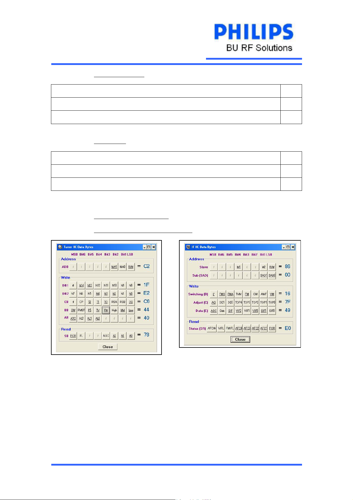
6.4.3.7.4 VIF LEVEL window
VIF LEVEL D6
VIF HIGH LEVEL (Above 25dBuV RF input) 1
VIF LOW LEVEL (Below 20dBuV RF input) 0
6.4.3.7.5 AFC window
AFC WINDOW D7
VCO inside AFC window (Within +/- 1.6MHz) 1
VCO outside AFC window (Outside +/- 1.6MHz) 0
6.4.4 I2C Bus Programming examples
6.4.4.1 Examples 1, tune to PAL B/G (at 471.25MHz)
FQ/FM1200MK3 Application note 22
Page 23
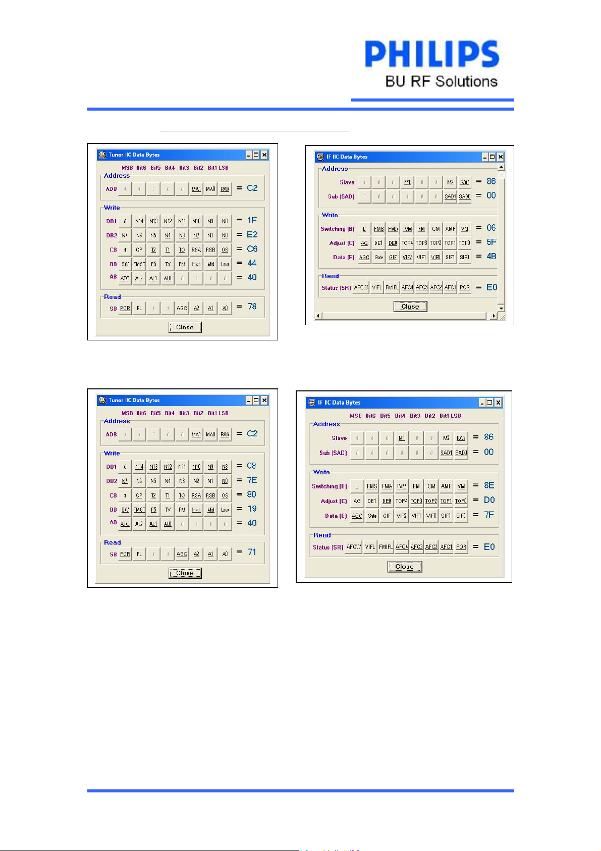
6.4.4.2 Examples 2, tune to SECAM L mode (at 471.25MHz)
6.4.4.3 Examples 3, tune to FM Radio mode (at 98.0MHz)
FQ/FM1200MK3 Application note 23
Page 24
6.5 Specific pin Connections
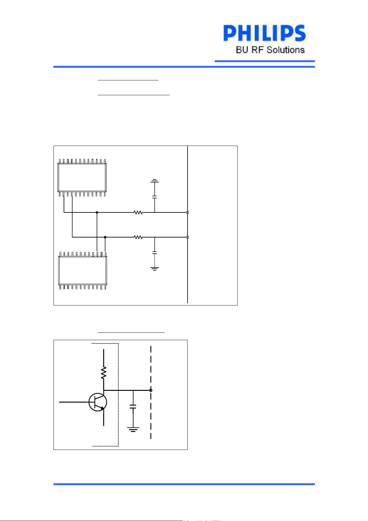
6.5.1 Loading of I
The SDA and SCL lines are already contain series impedances of 200 Ohms and parallel
capacitances of 22 pF inside the module. Therefore, Care must be taken to ensure that the total
load on the I
to use it”
IF Section
Tuner Section
Figure 5, I2C loading
6.5.2
Stereo
Decoder IC
Figure 6, AF-R/AF-L Pins
2
C Bus does not exceed that mentioned in the I2C brochure “ The I2C-bus and how
AF-R / AF-L (Pin9 /pin 10)
5V
5k
2
C Bus (pins 4/5)
12n
200ohms
200ohms
22pF
22pF
Pin 9/10
AF-R/AF-L
2
I
C-Serial Clock
Pin 4
Pin 5
2
C-Serial Data
I
FQ/FM1200MK3 Application note 24
Page 25
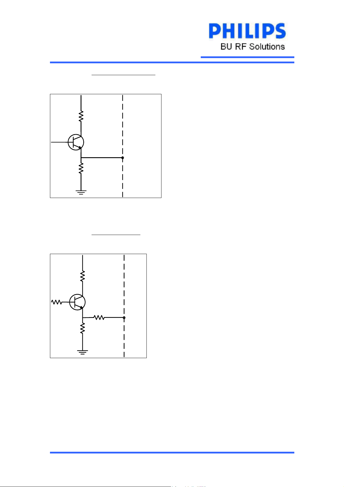
6.5.3 2nd IF Sound Output (pin11)
The 2nd IF Sound is intended for the Stereo Sound applications.
5V
10R
Pin 11
nd
2
IF Sound
820R
Figure 7, 2nd IF Sound Output
6.5.4 CVBS Load (Pin 12)
A video buffer is built into the frontend to enable the module to drive a 75ohms load directly.
5V
10R
100R
75R
220R
Pin 12
CVBS
Figure 8, CVBS Output
FQ/FM1200MK3 Application note 25
Page 26
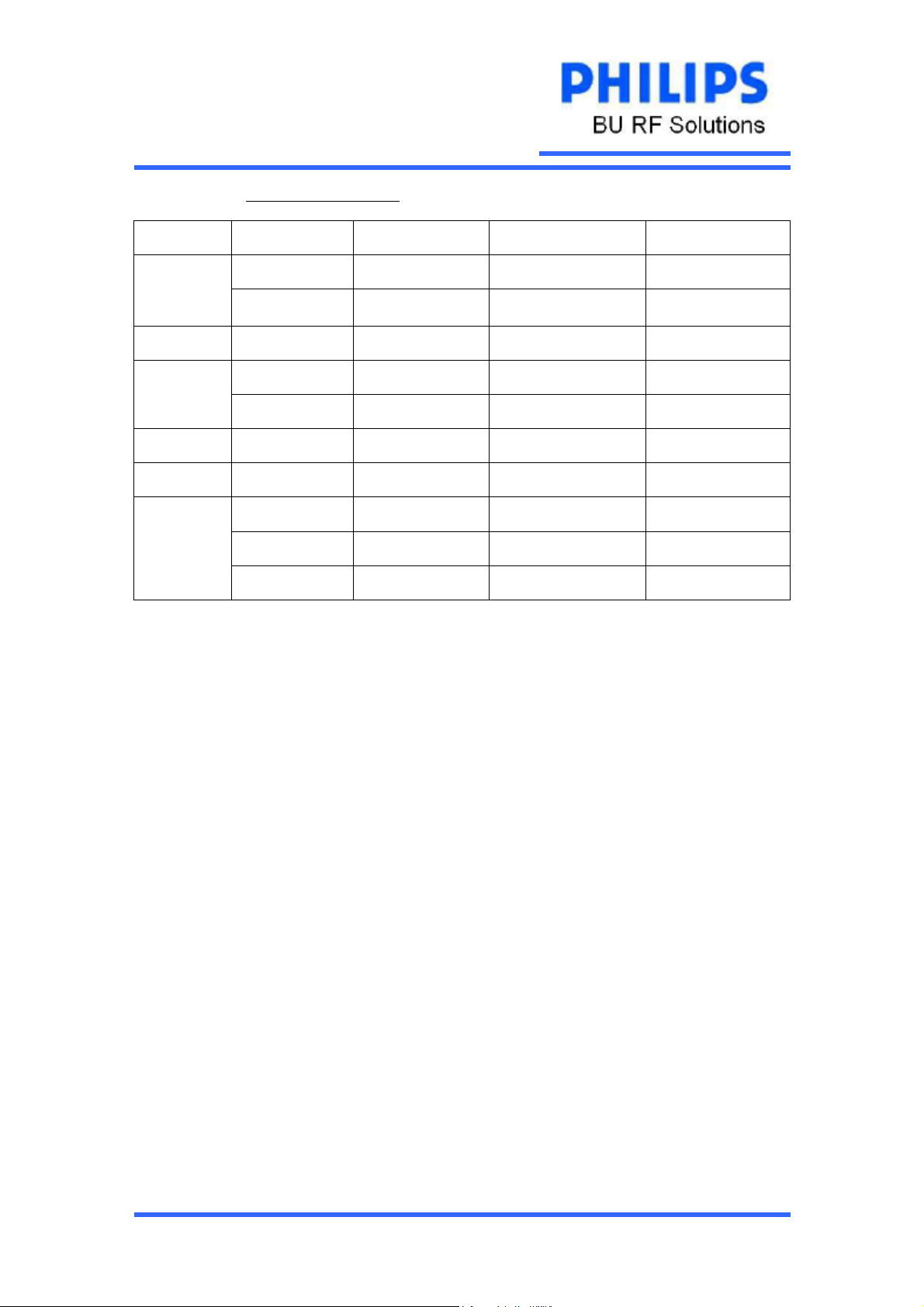
6.6. TV Stereo Sound System
nd
TV System Sound carrier 2
5.5 MHz 5.742 MHz FM-Stereo (A2) Germany; Malaysia
B/G
5.5 MHz 5.85 MHz FM-Mono/ NICAM
I 6.0 MHz 6.552 MHz FM-Mono/ NICAM UK, Hong Kong
6.5 MHz 6.258 MHz FM-Stereo (A2, D/K1) Slovak. Rep
D/K
6.5 MHz 5.85 MHz FM-Mono/ NICAM China, Hungary
L 6.5 MHz 5.85 MHz AM-Mono/NICAM France
4.5 MHz 4.724 MHz FM-Stereo (A2) Korea
Sound Carrier Sound Modulation Remarks
Scandinavia,
Singapore
M
4.5 MHz - FM-FM(EIA-J) Japan
4.5 MHz - BTSC-Stereo + SAP USA, Taiwan
The above table show the different audio systems used in the various TV Systems. The FQ/FM1200
MK3 can provide the necessary applications to recover the Stereo audio output.
The AF output at pin 14 provides the TV mono audio signal as well as the AM-MPX signal for the
BTSC and EIA-J.
There are ICs that support the BTSC and EIA-J Stereo sound. Philips Semiconductors, the
TDA9850/9852/9855 series and the SBX1637A/SBX1673 modules from SONY, can be connected
directly from pin 14 of FQ/FM1200MK3.
For other Audio systems, like NICAM and 2 Carrier FM Stereo, the 2
nd
Sound IF at pin 11 which is
internally buffered, it can be AC-coupled directly to the input of the specific ICs for Stereo sound
decoding.
Philips Semiconductors IC TDA9874/9875 and SAA7284 are able to take in the 2
nd
Stereo sound decoding.
The SAA7134 Video/PCI decoder has the function of Stereo sound decoding for NICAM/ FM-FM
(A2),
The SAA7133 Video/PCI decoder has the function of BTSC and EIA-J Stereo Sound decoding
nd
using 2
Sound IF input.
6.7 Approbation
The FQ/FM1200 MK3 family fulfils a wide range of regulations including FCC, CISPR, JIS,
DOC, BZT and CENELEC (EN55013 and EN55020). However, the final approbation is always
given for the complete receiver unit like, TV set, TV box, PC equipped with a TV/PCA card.
Basic requirement for FCC compliance is the tuner Noise Figure of less than 14dB.
Sound IF for
FQ/FM1200MK3 Application note 26
Page 27
7.0 Appendix
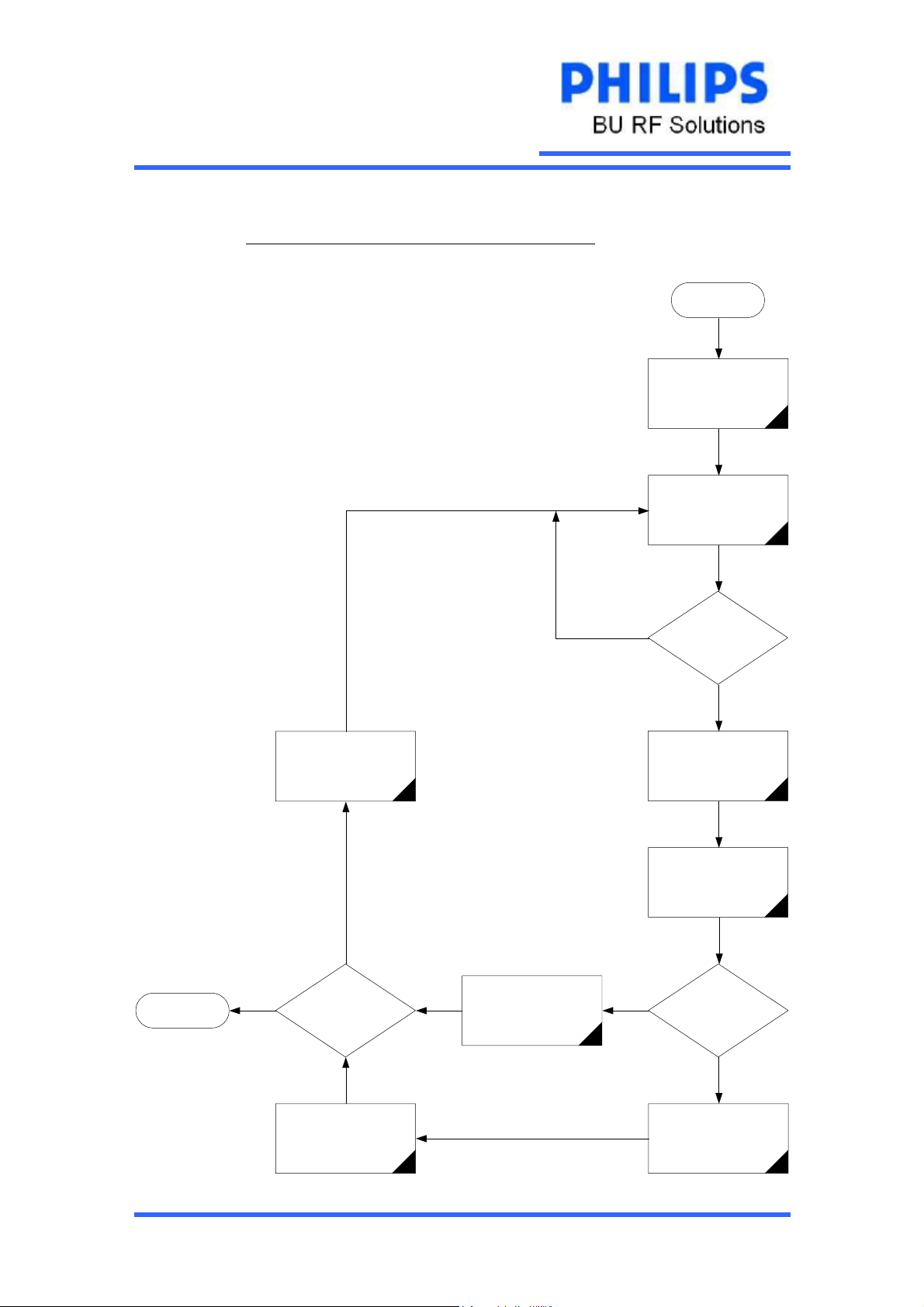
7.1. Appendix A: Recommended TV Auto-tuning flow chart
Start
Tune to first channel
(eg.48.25MHz/ PAL
System)
Read Lock Bit FL
from PLL Status Byte
Stop
Tune to new frequency
IS frequency
yes
above last
channel?
no
Increment frequency
by 0.25MHz
Is PLL Locked
no
no
(Status Byte
Delay 50ms.
Read AFC
Bits(D4;D3;D2;D1)
and VIFL bit
Is AFT within
62.5kHz window
and VIFL= ?1
FL=1)?
yes
yes
Increment frequency
by one channel
Store current channel
FQ/FM1200MK3 Application note 27
Page 28
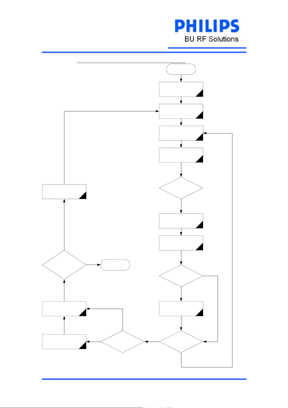
7.2 Appendix B: Recommended FM Auto-tuning flow chart
Tune FM to
new frequency
Start
Tune FM
from 87.5MHz
Counter = 0
Iteration = 0
Iteration = Iteration+1
Read PLL Locked Byte
no
Is PLL Locked
( FL=1)?
yes
no
Is frequency >
108MHz?
Increment frequency
by 100kHz
Store current channel
yes
yes
Stop
no
Counter > 8 ?
Delay 50ms
Read AFC
Bits(D4;D3;D2;D1)
and FMIFL bit
Is AFT within
+/-62.5kHz window
and FMIFL= 1?
yes
Counter = Counter+1
yes
Iteration >10 ?
no
no
FQ/FM1200MK3 Application note 28
Page 29
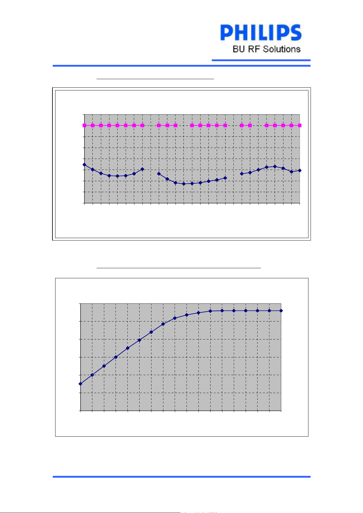
7.3 Appendix C: FQ1236 MK3 Noise Figure (FCC)
TUNER NOISE FIGURE FQ1236MK3
16
14
12
10
8
6
4
Noise Figure dBe
2
0
5
2
55.
5
2
83.
121.25
145.25
175.25
247.25
Frequency (MHz)
313.25
409.
25
471.25
549.25
723.25
801.25
7.4 Appendix D: Video SNR (CCIR 567 Weighted) Vs RF Input Level
VIDEO SNR vs INPUT SIGNAL (wgt acc CCIR 567, colourbar)
60
50
40
30
SN (dB)
20
10
0
20 30 40 50 60 70 80 90 100
Input Signal (dBuV)
FQ/FM1200MK3 Application note 29
 Loading...