

Page 1

Colour Television Chassis
FM242
AB
Contents Page Contents Page
1 Technical Specifications, Connections, and 2
Chassis Overview
2 Safety Instructions, Maintenance, Warnings, 5
and Notes
3 Directions for Use 7
4 Mechanical Instructions 10
5 Service Modes, Error Codes, Fault Finding, 13
and Repair Tips
6 Block Diagrams, Test Point Overviews, and Wiring
Diagram
Block Diagram Video 19
Block Diagram Audio 20
Power Lines Overview 21
2
I
C-IC Overview 22
Testpoint Overview Audio Amplifier 23
Testpoint Overview Power Supply 24
Testpoint Overview SCAVIO Panel 25
Wiring Diagram 26
7 Electrical Diagrams and PWB lay-outs Diagram PWB
Audio Amplifier: DC Protection (Diagram A1) 27 34-35
Audio Amplifier: Filters (Diagram A2) 28 34-35
Audio Amplifier: Left High (Diagram A3) 29 34-35
Audio Amplifier: Left Low (Diagram A4) 30 34-35
Audio Amplifier: Right High (Diagram A5) 31 34-35
Audio Amplifier: Right Low (Diagram A6) 32 34-35
Audio Amp: Supply + DC Prot. (Diagram A7) 33 34-35
LED/Switch Panel (Diagram LD) 36 37
LED Panel Display (Diagram LD) 38 39
SCAVIO: Function Blocks (Diagr. SC1) 40 55-60
SCAVIO: Sync Selection (Diagr. SC2) 41 55-60
SCAVIO: Video Select.ion (Diagr. SC3) 42 55-60
SCAVIO: Video ADC (Diagr. SC4) 43 55-60
SCAVIO: Video Select. Decoder (Diagr. SC5) 44 55-60
SCAVIO: VGA Input (Diagr. SC6) 45 55-60
©
Copyright 2003 Philips Consumer Electronics B.V. Eindhoven, The Netherlands.
All rights reserved. No part of this publication may be reproduced, stored in a
retrieval system or transmitted, in any form or by any means, electronic,
mechanical, photocopying, or otherwise without the prior permission of Philips.
SCAVIO: Control Functions 1 (Diagr. SC7) 46 55-60
SCAVIO: Control Functions 2 (Diagr. SC8) 47 55-60
SCAVIO: Scaler Clock Gen. (Diagr. SC9) 48 55-60
SCAVIO: PW Scaler + Memory (Diagr. SC10) 49 55-60
SCAVIO: Back-End EPLD (Diagr. SC11) 50 55-60
SCAVIO: Back-End LVDS Out (Diagr. SC12) 51 55-60
SCAVIO: Audio Source Select. (Diagr. SC13) 52 55-60
SCAVIO: Audio Processor (Diagr. SC14) 53 55-60
SCAVIO: Audio Delay Line (Diagr. SC15) 54 55-60
VGA Connector Panel (Diagr. VGA) 61 62-63
8 Electrical Alignments 65
9 Circuit Descriptions 68
List of Abbreviations 79
10 Spare Parts List 81
11 Revision List 89
Published by RB 0367 Service PaCE Printed in the Netherlands Subject to modification EN 3122 785 14130
Page 2
EN 2 FM242 AB1.
Technical Specifications, Connections, and Chassis Overview
1. Technical Specifications, Connections, and Chassis Overview
1.1 Technical Specifications
1.1.1 Picture
Display : SDI plasma panel
Screen size : 42" (106 cm)
Resolution : 852 x 480 pixels (pixel
pitch 1.095 x 1.11
mm)
Contrast ratio : 1000 : 1
1.1.2 Sound
Maximum power : 30 Wrms (for version
with speakers)
1.2 Connections
1.2.1 Rear Connections
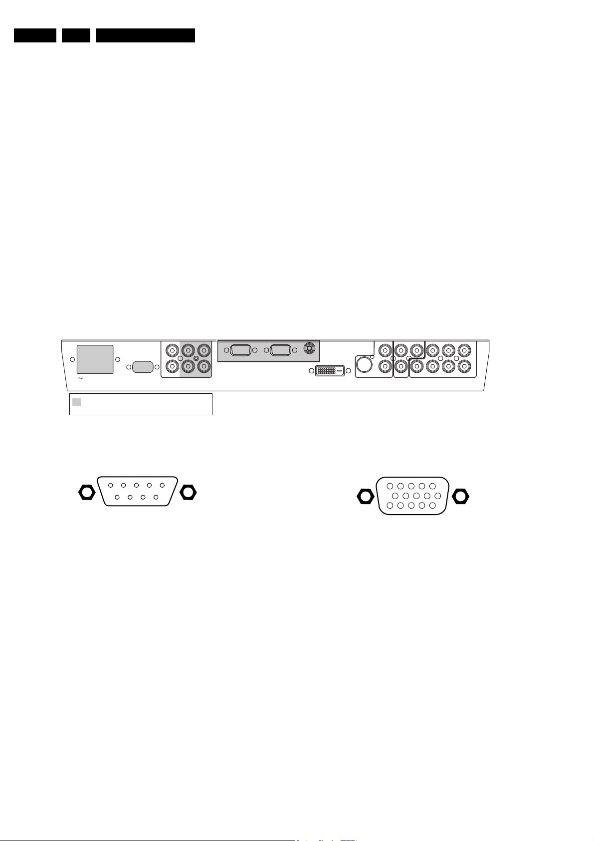
AUDIO IN
L
R
MAINS
! All Functional blocks shaded grey are r equired for
the"Basic Configuration".
The remainder is required f or the "Enhanced Configuration".
RS323
DVI-D
VGA2 VGA1
1.1.3 Miscellaneous
VGA1 VGA2 RC-OUT
Mains voltage : 95 - 264 V
Mains frequency : 50/60 Hz
Ambient temperature : + 5 to + 40 deg. C
Maximum humidity : 90% R.H.
Power consumption : around 380 W
Standby Power consumption : < 2 W
Weight : 35 kg
Dimensions (WxHxD) : Speakered version:
1215 x 657 x 90 mm
: Speaker-less version:
1070 x 660 x 90 mm
DVI-D
Y/C S
SVHS
AV2 AV1
L
R
AUDIOINAUDIO
CVBSB/Pb/Cb
IN
H
L
AV3
B/Pr/Cr
CL 16532099_010.eps
R
v
AUDIO
IN
260801
Figure 1-1 Rear Connections
RS232
1
6
5
9
Figure 1-2 RS232 connector (subD-9p)
1-
2 -TXD (UART) k
3 -RXD (UART) j
4 -RL_ICN (ICONN) j
5 - Ground H
6 -GL_ICN (ICONN) k
7 -LD_ICN (ICONN) k
8 -IR_TX (ICONN) k
9 -IR_RX (ICONN) j
10 - Ground H
11 - Ground H
Audio - In (DVI-D)
1 -Audio - L 0.5 Vrms / 1 kΩ jq
2 -Audio - R 0.5 Vrms / 1 kΩ jq
Audio - In (VGA2)
1 -Audio - L 0.5 Vrms / 1 kΩ jq
2 -Audio - R 0.5 Vrms / 1 kΩ jq
VGA1 - In
1
6
11
5
10
15
Figure 1-3 VGA Connector
1 - Red 0.7 Vpp / 75 Ω j
2 - Green 0.7 Vpp / 75 Ω j
3 - Blue 0.7 Vpp / 75 Ω j
4-TXD k
5 - Ground H
6 - Red Ground H
7 - Green Ground H
8 - Blue Ground H
9-RC k
10 - Ground H
11 - RXD j
12 - DDC_SDA j
13 - H-sync 0 - 5 V j
14 - V-sync 0 - 5 V j
15 - DDC_SCL j
Audio - In (VGA1)
1 -Audio - L 0.5 Vrms / 1 kΩ jq
2 -Audio - R 0.5 Vrms / 1 kΩ jq
Page 3
Technical Specifications, Connections, and Chassis Overview
EN 3FM242 AB 1.
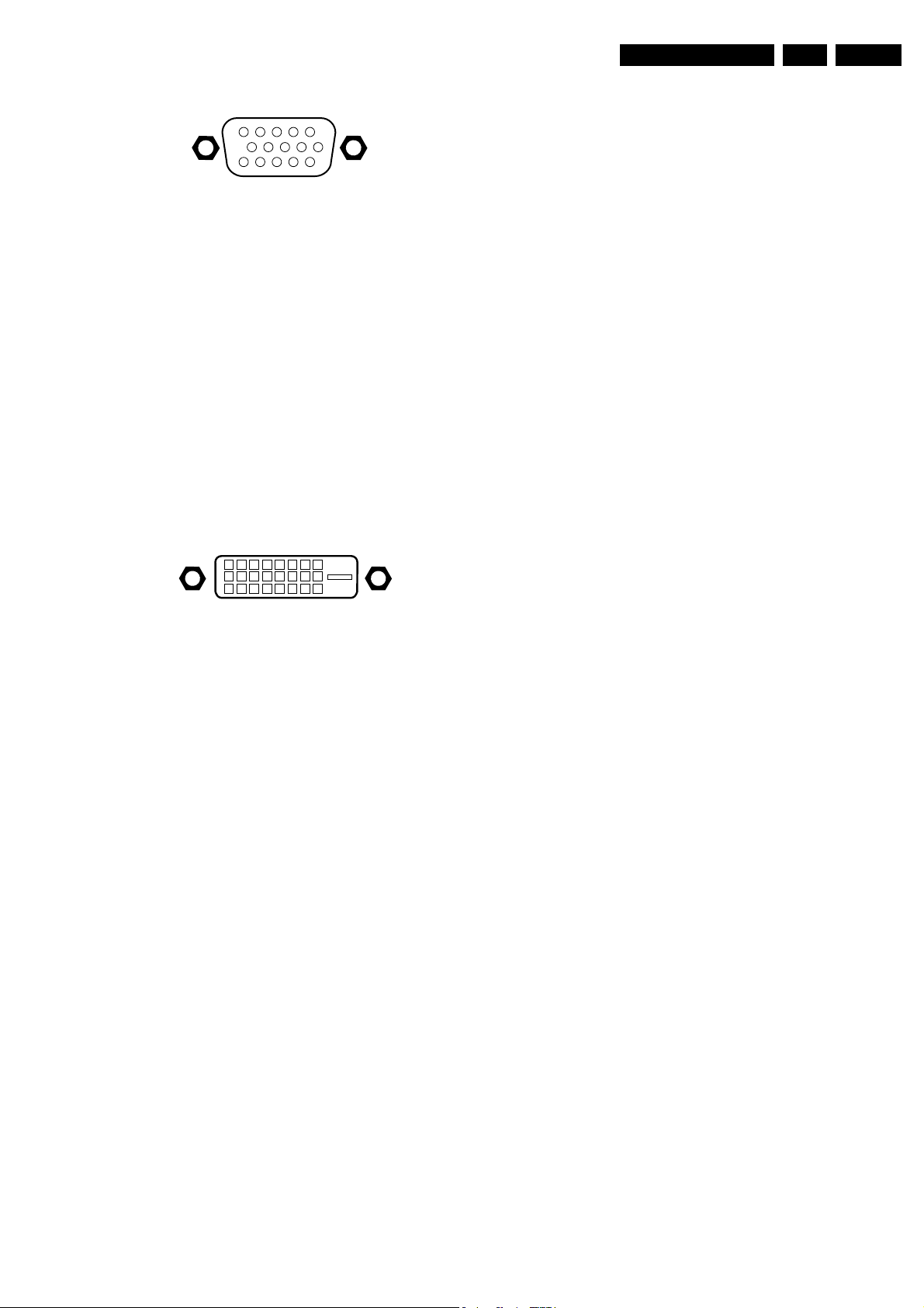
VGA2 - Out
1
6
11
5
10
15
Figure 1-4 VGA Connector
1 - Red (0.7 Vpp/75 Ω) kj
2 - Green (0.7 Vpp/75 Ω) kj
3 - Blue (0.7 Vpp/75 Ω) kj
4-TXD k
5 - Ground H
6 - Red Ground H
7 - Green Ground H
8 - Blue Ground H
9-
10 - Ground H
11 - RXD j
12 - DDC_SDA j
13 - H-sync 0 - 5 V kj
14 - V-sync 0 - 5 V kj
15 - DDC_SCL j
RC - Out
1-RC kq
DVI-D
18
916
17
C5
24
AV1: Audio/Video - In
1 - CVBS 1 Vpp / 75 Ω jq
2 - Audio - L 0.5 Vrms / 10 kΩ jq
3 - Audio - R 0.5 Vrms / 10 kΩ jq
AV3: Audio/Video - In
1 - G/Y/Y 0.7 Vpp / 75 Ω jq
2 - B/Pb/Cb 0.7 Vpp / 75 Ω jq
3 -R/Pr/Cr 0.7 Vpp / 75 Ω jq
4-H jq
5-V jq
6 - Audio - L 0.5 Vrms / 10 kΩ jq
7 - Audio - R 0.5 Vrms / 10 kΩ jq
Figure 1-5 DVI-D Connector
1-RX2- j
2-RX2+ j
3 - Ground H
4-
5-
6 -DDC-SCL k
7 - DDC-SDA k
8-
9-RX1- j
10 - RX1+ j
11 - Ground H
12 -
13 -
14 - 5V_STBY_SW
15 - Ground H
16 - 5V_STBY_SW
17 - RX0- j
18 - RX0+ j
19 - Ground H
20 -
21 - Ground H
22 -
23 - RXC+ j
24 - RXC- j
C
5 - Ground H
AV2: SVHS - In
1 - Y Ground H
2 - C Ground H
3 - Y 1 Vpp / 75 Ω j
4 - C / 16:9 0.3 Vpp / 75 Ω j
AV2: Audio - In
1 - Audio - L 0.5 Vrms/10 kΩ jq
2 - Audio - R 0.5 Vrms/10 kΩ jq
Page 4
EN 4 FM242 AB1.
1.3 Chassis Overview
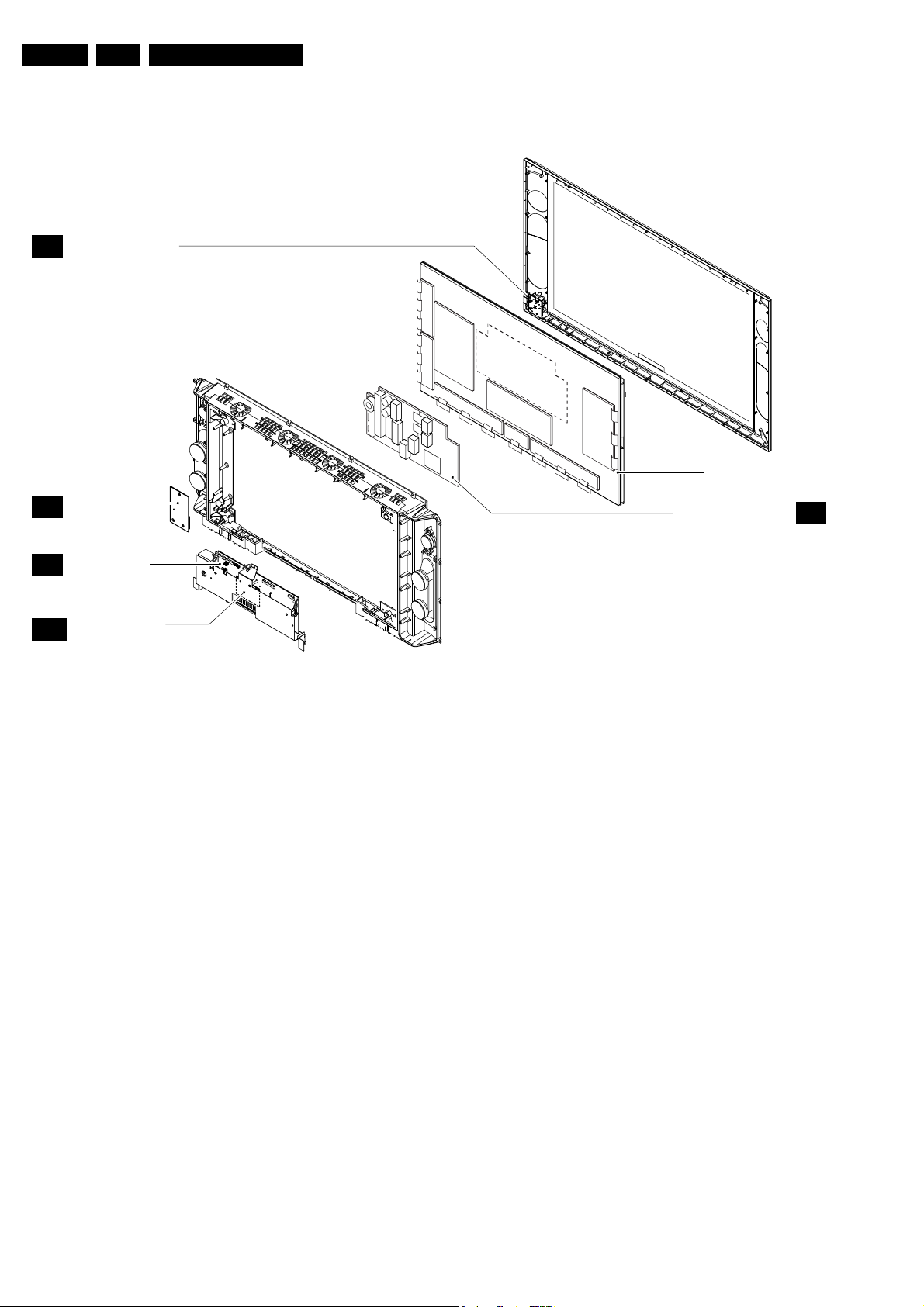
LED / SWITCH PANEL
LD
Technical Specifications, Connections, and Chassis Overview
Y-
Buffer
(up)
Y-M
ain
Y-
Buffer
(down)
A
SC
VGA
AUDIO AMPLIFIER
PANEL
SCAVIO PANEL
VGA CONNECTOR
PANEL
Logic-Buffer (E)
SMPS
Figure 1-6 PWB Location
Logic Board
Logic-
Buffer (F)
Logic-Buffer (G)
X- Board
PLASMA DISPLAY PANEL
POWER SUPPLY PANEL
CL 36532011_010.eps
P
060303
Page 5

Safety Instructions, Warnings, and Notes
2. Safety Instructions, Warnings, and Notes
EN 5FM242 AB 2.
2.1 Safety Instructions
Safety regulations require that during a repair:
• Connect the set to the mains via an isolation transformer
(> 800 VA).
• Do not operate the monitor without the front glass plate.
One function of this glass plate is to absorb IR radiation.
Without this glass plate, the level of radiation could
damage your eyes.
• Replace safety components, indicated by the symbol h,
only by components identical to the original ones.
Safety regulations require that after a repair, the set must be
returned in its original condition. Pay, in particular, attention to
the following points:
• Route the wire trees correctly and fix them with the
mounted cable clamps.
• Check the insulation of the mains lead for external
damage.
• Check the electrical DC resistance between the mains plug
and the secondary side (only for sets which have a mains
isolated power supply):
1. Unplug the mains cord and connect a wire between the
two pins of the mains plug.
2. Set the mains switch to the "on" position (keep the
mains cord unplugged!).
3. Measure the resistance value between the pins of the
mains plug and the metal shielding of the tuner or the
aerial connection on the set. The reading should be
between 4.5 MΩ and 12 MΩ.
4. Switch "off" the set, and remove the wire between the
two pins of the mains plug.
• Check the cabinet for defects, to avoid touching of any
inner parts by the customer.
2.2 Warnings
• All ICs and many other semiconductors are susceptible to
electrostatic discharges (ESD w). Careless handling
during repair can reduce life drastically. Make sure that,
during repair, you are connected with the same potential as
the mass of the set by a wristband with resistance. Keep
components and tools also at this same potential.
Available ESD protection equipment:
– Complete kit ESD3 (small tablemat, wristband,
connection box, extension cable and earth cable) 4822
310 10671.
– Wristband tester 4822 344 13999.
• Be careful during measurements in the high voltage
section.
• Never replace modules or other components while the unit
is switched "on".
• When you align the set, use plastic rather than metal tools.
This will prevent any short circuits and the danger of a
circuit becoming unstable.
2.3 Notes
• Clean the glass plate in front of the plasma display with a
slightly humid cloth. If, due to circumstances, there is some
dirt between the glass plate and the plasma display, this
must be cleaned by a qualified service engineer (see
section “Mechanical Instructions”).
• Measure the direct voltages and oscillograms with regard
to the chassis ground (H), or hot ground (I) as this is
called.
• The direct voltages and oscillograms shown in the
diagrams are indicative. Measure them in the Service
Default Mode (see section “Service Modes”).
• Where necessary, measure the voltages in the power
supply section both in normal operation (G) and in standby
(F). These values are indicated by means of the
appropriate symbols.
• The semiconductors indicated in the circuit diagram and in
the parts lists, are interchangeable per position with the
semiconductors in the unit, irrespective of the type
indication on these semiconductors
2.3.1 Schematic Notes
• All resistor values are in ohms and the value multiplier is
often used to indicate the decimal point location (e.g. 2K2
indicates 2.2 kOhm).
• Resistor values with no multiplier may be indicated with
either an "E" or an "R" (e.g. 220E or 220R indicates 220
Ohm).
• All Capacitor values are expressed in Micro-Farads (µ =
-6
x10
), Nano-Farads (n = x10-9), or Pico-Farads (p = x10
12
).
• Capacitor values may also use the value multiplier as the
decimal point indication (e.g. 2p2 indicates 2.2 pF).
• An "asterisk" (*) indicates component usage varies. Refer
to the diversity tables for the correct values.
• The correct component values are listed in the Electrical
Replacement Parts List. Therefore, always check this list
when there is any doubt.
2.3.2 Rework on BGA ICs
General
Although (LF)BGA assembly yields are very high, there may
still be a requirement for component rework. By rework, we
mean the process of removing the component from the PWB
and replacing it with a new component. If an (LF)BGA is
removed from a PWB, the solder balls of the component are
deformed drastically so the removed (LF)BGA has to be
discarded.
Device removal
As is the case with any component, it is essential when
removing an (LF)BGA that the board, tracks, solder lands, or
surrounding components are not damaged. To remove an
(LF)BGA, the board must be uniformly heated to a temperature
close to the reflow soldering temperature. A uniform
temperature reduces the chance of warping the PWB.
To do this, we recommend that the board is heated until it is
certain that all the joints are molten. Then carefully pull the
component off the board with a vacuum nozzle. For the
appropriate temperature profiles, see the IC data sheet.
Area preparation
When the component has been removed, the vacant IC area
must be cleaned before replacing the (LF)BGA.
Removing an IC often leaves varying amounts of solder on the
mounting lands. This excessive solder can be removed with
either a solder sucker or solder wick. The remaining flux can be
removed with a brush and cleaning agent.
After the board is properly cleaned and inspected, apply flux on
the solder lands and on the connection balls of the (LF)BGA.
Note: Do not apply solder paste, as this has shown to result in
problems during re-soldering.
-
Page 6

EN 6 FM242 AB2.
Device replacement
The last step in the repair process is to solder the new
component on the board. Ideally, the (LF)BGA should be
aligned under a microscope or magnifying glass. If this is not
possible, try to align the (LF)BGA with any board markers.
To reflow the solder, apply a temperature profile according to
the IC data sheet. So as not to damage neighbouring
components, it may be necessary to reduce some
temperatures and times.
Safety Instructions, Warnings, and Notes
Page 7
3. Directions for Use
22
VGA 640x480 60, 72, 75, 85 Hz
Wide VGA 848x480 60 Hz
Wide VGA 852x480 60 Hz
MAC 640x480 66.67 Hz
MAC 832x624 74.55 Hz
MAC 1024x768 74.93 Hz
MAC 1152x870 75 Hz
SVGA 800x600 56, 60, 72, 75, 85 Hz
XGA 1024x768 60, 70,75, 85 Hz
SXGA 1280x1024 60,72 Hz
Monitor Display modes
Operation
&
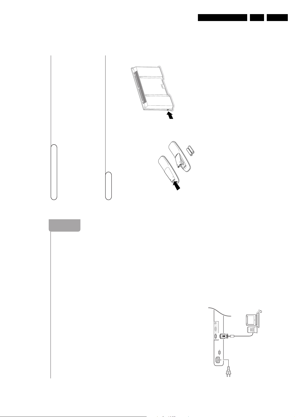
Insert the mains plug supplied into the
mains inlet at the back of the monitor and in
the wall socket.
For safety, please, only use the supplied rim-earthed
mains cord which has to be inserted in a grounded
socket.éRemote control: remove the cover of the
battery compartment.
Insert the 2 batteries supplied (Type R6/AA-
1.5V).
The batteries supplied do not contain the heavy
metals mercury and cadmium. Nevertheless in
many countries batteries may not be disposed of
with your household waste. Please check on how to
dispose of batteries according to local regulations.“Make sure that your electronic receiver box
and/or PC are switched on and that your PC is
in the correct display mode.
When a VGA computer is connected,the
display selection is made automatically.
A message is displayed when the monitor does
not support the connected VGA mode. Switch
your computer to a correct display mode.
‘
Switch the monitor on : Press the on/off
key B at the right side of the monitor.
A green indicator lights up and the screen
comes on.
When the monitor does not receive a
supported VGA signal and is not connected to
a receiver box, the screen switches to standby
and the red indicator lights up.
When you switch on your monitor for the
first time, and the monitor is not connected
to an electronic receiver box,the language
menu automatically appears on the screen.The
explanation appears in different languages one
at a time.
Follow the instructions on screen to select the
correct language or see Setup menu, Language,
p. 5.
R6 / AA
B
1
English
Unpacking and wall mounting
instructions
For the unpacking instructions follow the
illustrated steps printed on the packaging
(outside and inside). For the wall mounting
instructions follow the illustrated steps ‘
to § printed on the separate leaflet.
Make sure that the wall mount is being fixed
securely enough so that it meets safety
standards.The weight of the monitor (excl.
packaging) is about 35 kg.
Note: Stands are optional accessories. Consult
your dealer.
Connect your electronic receiver box
See the separate supplied instruction manual
with your receiver box.
Connect your computer
To the receiver box
See the illustration in the inside frontcover of
this handbook.
Connect one end of a VGA cable to the
video card of the computer and the other
end to the
VGA IN
connector at the rear
side of the receiver box. Fix the connectors
firmly with the screws on the plug.
Directly to the monitor
& Connect one end of a VGA cable to the
video card of the computer and the other
end to the
VGA 1
connector at the rear side
of the monitor.Fix the connectors firmly with
the screws on the plug.
Daisy chaining
The Loop Through facility makes it
possible to make a daisy chain with a
second monitor.
é Connect one end of another VGA cable to
the
VGA 2
connector at the rear side of
the monitor and the other end to the
VGA 1
connector of a second monitor.
The RC out jack next to the VGA 2 connector
makes it possible to daisy chain
remote control signals to other equipment.
This output cannot be used to daisy chain a
second monitor.
Serial I/O port RS232
The RS232 connector is only to be used
with the monitor as stand alone.
This connector allows you to control the
monitor via your PC (as a replacement of
the remote control).
Note:This connector can also be used for
dealer service tools.
Directions for Use
EN 7FM242 AB 3.
RC OUT
VGA 2
VGA 1
RS232
~ MAINS
Page 8
EN 8 FM242 AB3.
4
&
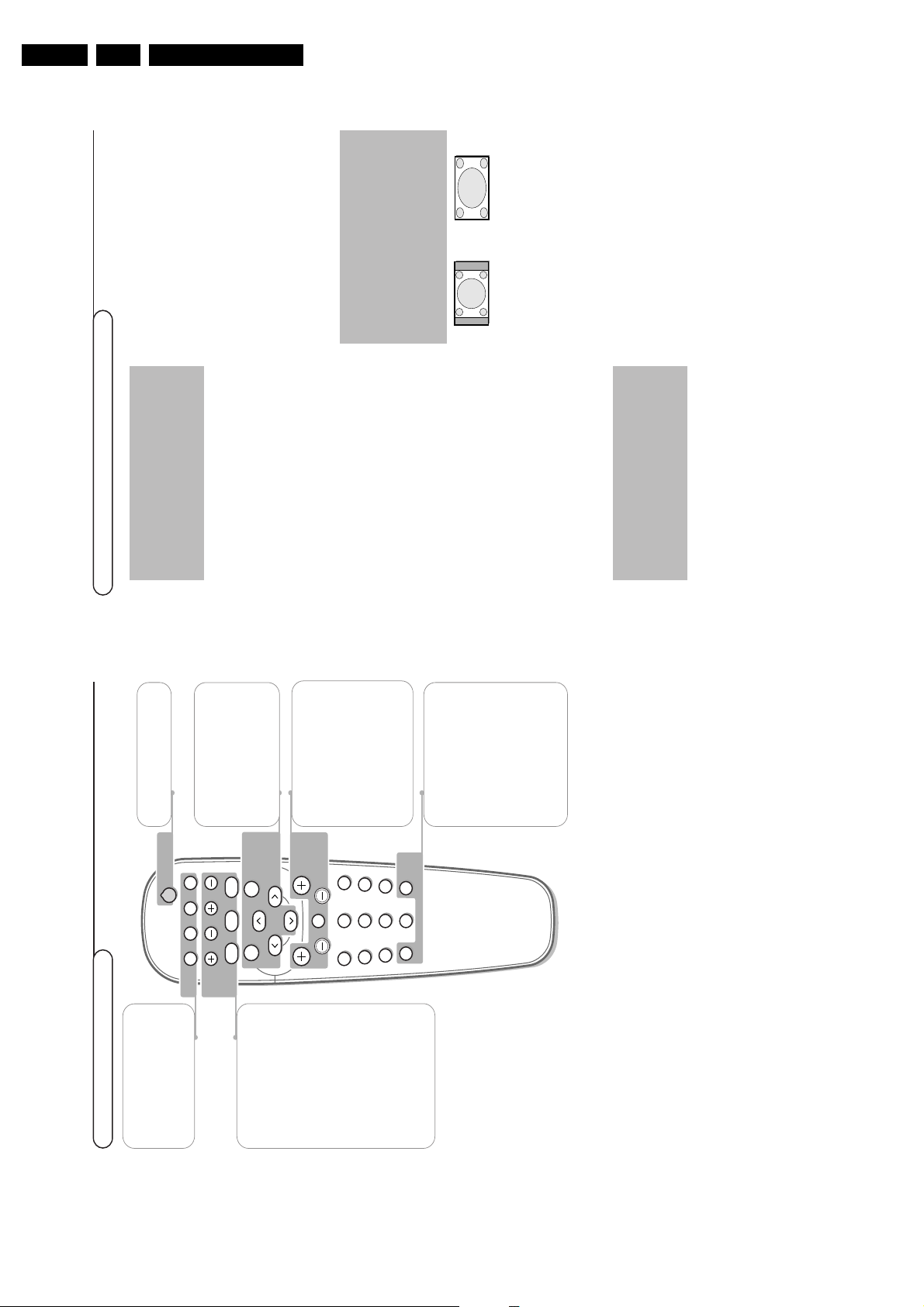
Press the MENU key on the remote control to
summon the different menu headers.
é
Press the cursor left/right to move the cursor
horizontally through the menu headers.“Press the cursor down to access the menu.
In case of a slider,move the cursor left/right to
adjust.
In case of a list with options, move the cursor
right to enter and use the cursor up/down to
select an option.
Press the cursor left to leave the options list.
‘
Press the MENU key again to switch off the
menu.
Note: Sometimes not all the menu items are visible
on the screen.
Press the cursor down until all the items are
displayed.
Only when the US English language has been
selected (see Setup menu,
Language, p. 5), the menu items will be displayed
with additional icons.
Operation
Press the MENU key on the remote control to
summon the main menu.
Picture 1 menu
Use of the menus and the menu system
Contrast
This control allows you to adjust the contrast
level of the picture.
Colour temperature
This control allows you to select the colour
temperature of the picture.
Move the cursor up/down to make a selection.
Press the cursor left to return to the Picture 1
menu.
Sharpness
This control allows you to adjust the edge
definition of a picture.
Picture 2 menu
In this menu you are allowed to adjust
attributes which are relevant for the picture on
the display, like format, zoom, size, etc.
Format
Select Format to summon a list of available
display formats for showing images in the
traditional 4:3 proportions.
Press the cursor up/down to select another
display format: 4:3 or Wide screen.
Zoom
Select Zoom On to activate the zoom
function.
You may also activate the zoom function with
the ZOOM ON/OFF key on the remote
control.
Press the cursor left/right, up/down to select
which part of the screen will be zoomed.
4:3
Wide screen
Picture 1
Brightness
Contrast
Colour temperature
Sharpness
Picture 2
Format
‡
4:3
Zoom Wide screen
Zoom factor
Shift
Clock frequency
Phase
Auto align
Brightness
Contrast
Colour temp.
Sharpness
Picture 1 Picture 2 Setup
Brightness
This control allows you to adjust the
brightness level of the picture.
33
POWER
BRIGHTNESS
CONTRAST
ZOOM OUTZOOM INZOOM ON/OFF
VGA AV1 AV2 AV3
MUTE
AV MUTE
q
1
2
3
4
5
6
7
8
9
0
V
CH/PR
MENU
OK
¬
B
VGA to select your
computer connected to the
VGA 1 connector
AV1 , AV2, AV3 no function
BRIGHTNESS +/-
to adjust the brightness level
of the picture
CONTRAST +/-
to adjust the contrast level of
the picture
ZOOM ON/OFF to
activate/de-activate the zoom
function. See p. 4.
ZOOM IN/OUT to adjust
the zoom factor and to
change the magnification of
the picture when zoom is
activated. See p. 4.
V
press - or + to adjust
the volume
¬
no function (except
when in combination with a
receiver box and a Home
Cinema audio receiver)
CH/PR
Programme
selection
To browse through the
sources selected.
B
to switch to standby or
on again
MENU to switch the menu
on/off
cursor keys to select your
choice and to alter a selected
adjustment.
OK to activate your choice
AV MUTE to temporarily
mute the picture and the
sound or restore it.
When activated a yellow
indicator starts blinking in
front of the monitor.
q Picture format
See Picture 2 menu, p. 4.
Press the q key to switch
between the different picture
formats.
Use of the remote control
If your monitor no longer responds to the
remote control, the batteries may be exhausted.
How to dispose of batteries ?
The batteries supplied do not contain the heavy
metals mercury and cadmium. Nevertheless in
many countries batteries may not be disposed of
with your household waste. Please ensure you
dispose of batteries according to local regulations.
End of life directives
Philips is paying a lot of attention to produce
environmentally-friendly in green focal areas.
Your new monitor contains materials which can
be recycled and reused.
At the end of its life specialised companies can
dismantle the discarded monitor to concentrate
the reusable materials and to minimise the
amount of materials to be disposed of.
Please ensure you dispose of your old monitor
according to local regulations.
Directions for Use
Page 9
Directions for Use
6
Ambient temperature
Do not hang up the monitor
above a central heating or other
heating sources.
Care of the screen
Clean the anti-reflex coated flat
glass screen with a slightly damp
soft cloth. Do not use abrasives
solvents as it can damage the
glass surface of the screen.
Plasma Display
characteristics
Caution:A video source (such as
a video game, DVD,or video
information channel) which
shows a constant non-moving
pattern on the screen, can cause
damage to the screen.When your
Flat-Monitor is continuously used
with such a source, the pattern of
the non-moving portion of the
game (DVD, etc.) could leave an
image permanently on the screen.
When not in use, turn the video
source OFF.
Regularly alternate the use of
such video sources with normal
viewing.
When switching over to another
picture after having displayed the
same still picture for a long time
(many hours), it may happen that
some parts from the previous
picture will remain on screen due
to a kind of memory effect.This
ghost picture will disappear after
some time.To avoid this effect
change the pictures regularly or
for PC use you can turn on a
screen saver in your computer.
For video signals, Philips has built
in an automatic shift of the
picture every 5 minutes to avoid
this effect and to prolong the life
of the screen.
Very incidentally and after a
longer period of unuse (approx. 1
year) the screen may display
some strange colour deficiencies.
This is quite normal for plasma
displays and these effects will
disappear after the set has been
turned on for some time.
A plasma display consists of a
huge amount of colour pixels. It is
within industry standards that
very few pixels (< 0.001%) may
be defective, even for a new set.
There is however no reason to
doubt about the quality of the
set.
The plasma display technology
operates with rare gases which
are being influenced by air
pressure.
Up to an altitude of 2000 m
above sea-level (local air pressure
equal or above 800 hPa), the
display is functioning fine.
Operating the set at a higher
altitude (lower air pressure),the
picture becomes unstable and the
picture performance is
deteriorating. The plasma display
might then also produce a
humming sound.After bringing
the set below 2000 m (local air
pressure equal or above 800 hPa)
it works fine again.Transportation
has no influence.
Control of peripheral
equipment
The infrared signals of the screen
may influence the reception
sensitivity of other peripherals.
Solution: replace the batteries of
the remote control or change
position of other equipment. E.g.
keep away a wireless headphone
from within a radius of 1.5 m.
No stable or not
synchronised VGA
picture
Check if you have selected the
correct VGA mode in your PC.
No picture or no sound
Are the supplied cables
connected properly? (The power
cable to the display, the VGA
cables, the audio cables,...)
Is your PC or receiver box
switched on?
Do you see a black screen and
the indicator on front of the
monitor lights up green, this
means that the display mode is
not supported.
Switch your VGA source to a
correct mode.
If your problem is not solved:
Switch your monitor off and then
on again.
Never attempt to repair a
defective monitor yourself.
Check with your dealer or call a
video technician.
Transport
Keep the original packaging to
transport the monitor if needed.
Miscellaneous
. Ambient temperature:
+ 5 ~ + 40°C
. Maximum operating altitude:
2000 m (min. air pressure
800 hPa)
. Mains: Auto Voltage ranging from
95V to 264V 50Hz/60Hz
. Power consumption:
around 380 W
. Standby consumption: < 2 W
. Weight (excl. packaging)
Display: 35 kg
. Dimensions (wxhxd):
Display: 107 x 66 x 9cm
. Wall mounting bracket included
Tips
5
Zoom factor
Select Zoom factor and press the cursor
left/right to adjust the zoom factor and to
change the magnification of the picture.
If zoom is not active, Zoom Off,changing the
magnification factor will have no effect on the
displayed picture.
Shift
This control allows you, when necessary, to
move the picture in a horizontal or vertical way.
&
Use the cursor left/right to adjust.
é
Press the OK key when done.
Clock frequency
This control allows you, when necessary, to
adjust the values of the clock frequency so that
especially text can be displayed with an optimal
overall sharpness.
Use the cursor left/right to adjust.
Phase
This control allows you, when necessary, to
adjust the pixel phase of the picture to avoid
picture interference.
Use the cursor left/right to adjust.
Auto align
This control allows you to automatically adjust
the shift, the clock frequency and the phase in
VGA mode.
Press OK to execute.
Setup menu
&
Use the cursor down to select Language.éPress the cursor right to enter the list of
selectable languages.
“
Use the cursor up/down to scroll through the
list and to bring up other languages which are
not displayed on the screen at present.
Setup
Language US English
English
Nederlands
Deutsch
Français
Español
...
EN 9FM242 AB 3.
Page 10
EN 10 FM242 AB4.
Mechanical Instructions
4. Mechanical Instructions
Index of this chapter:
• Service Position Monitor
• Rear Cover Removal
• Service Position Panels
• PDP and Glass Plate Replacement
• Re-assembly
Note: Figures below can deviate from the actual situation, due
to different set executions.
4.1 Service Position Monitor
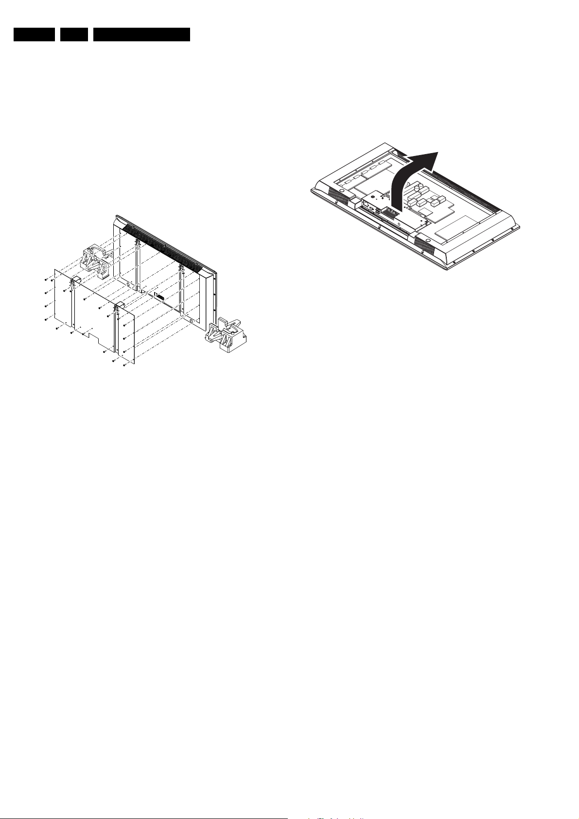
Figure 4-1 Service Position
First, put the monitor in its service position. (Can be done via
buffers as showed on figure, but preferable via new service
position solution as described below. Still some improvising is
needed for service positions panels however). Therefore,
disconnect all cables connected to the monitor and take the
monitor of the wall (or tabletop stand). Then, fix the monitor to
the 2 service-poles. (the 2 poles together form a service-kit:
3122 785 90480; this service-stand can be used for 30” until
42” FTVs.
CL 16532099_041.eps
250901
4.3 Service Position Panels
4.3.1 SCAVIO Panel
Solder-side SCAVIO
B
CL 36532011_011.eps
Figure 4-2 Service position SCAVIO (1)
To access the panel:
1. Remove the cables from connectors 0320, 0305, 0301,
0319 and 0388 on the SCAVIO panel.
2. Remove the power cable from the mains power inlet to the
power supply (connector 0308).
3. Remove the five screws at the bottom of the SCAVIOpanel cover plate.
4. Hold the SCAVIO panel while removing the top screw, in
order to prevent that it will fall.
5. Take the panel out, and turn it 180 degrees, so that you
face the solder side of the SCAVIO panel.
6. Reconnect all cables. Use a standard power cable to
connect the mains directly to PSU-connector 0308, and
use the "LED/Switch panel" service kit 3122 785 90410 (as
the original cable is too short).
Caution: When measuring, watch out for the "hot" left heat sink
of the PSU!
200303
4.2 Rear Cover Removal
To be able to access or measure the panels, remove the rear
cover (metal back plate):
Warning: make sure that the mains power is disconnected
before you remove the metal back plate.
1. Remove all fixation screws of the back plate, as indicated
in the figure above (five at the top, five at each side, seven
at the bottom and the two larger ones just below the "wall
mounting holes").
2. Remove the metal back plate. Make sure that wires and flat
foils are not damaged during plate removal.
Another way to measure the SCAVIO panel:
1. Remove the five screws at the bottom of the SCAVIOpanel cover plate.
2. Hold the SCAVIO panel while removing the top screw, in
order to prevent that it will fall.
3. Put a piece of paper (or cardboard) in front of the Power
Supply.
4. Take the panel out, and turn it upward [B], so that you face
the solder-side of the SCAVIO panel.
Caution: Make sure that the metal connector plate does not
touch any "hot" part of the Power Supply (heatsink).
Page 11
Mechanical Instructions
EN 11FM242 AB 4.
Component-side SCAVIO
CL 16532099_043.eps
250901
Figure 4-3 Service position SCAVIO (2)
To access the other side of the SCAVIO panel:
1. Disconnect all cables going to the SCAVIO panel.
2. Remove all screws at the connectors of the connector
plate, see figure "Solder-side SCAVIO".
3. Remove the three fixation screws that connect the SCAVIO
panel to the connector plate, see figure "Component-side
SCAVIO".
4. Reconnect the SCAVIO panel, be careful: do not make a
short-circuit!
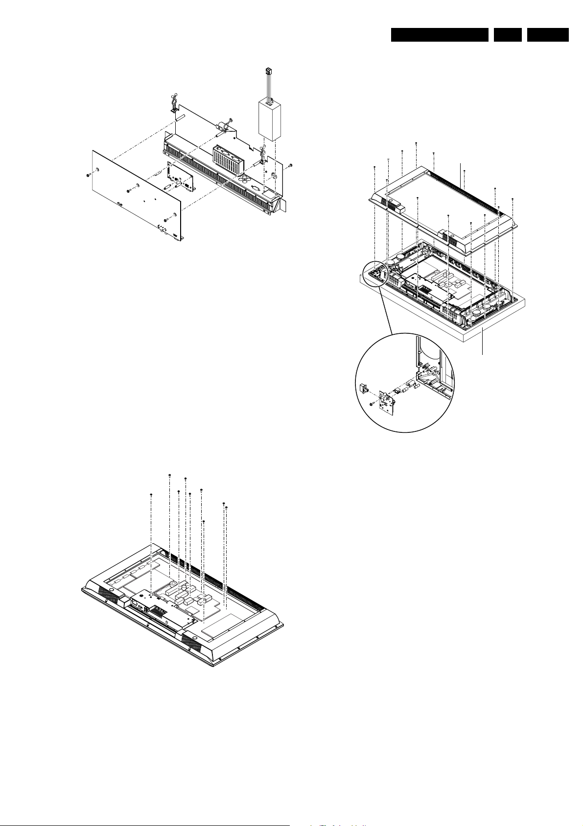
4.3.4 Audio Amplifier Panel (only valid for “speaker”-version)
The solder-side of this panel is directly accessible. To access
the component-side, or to remove the whole panel, unscrew
the three fixation screws
4.3.5 LED/Switch Panel and Speakers
Plastic backcover
Foam cushion
4.3.2 VGA Connector Panel
How to remove the VGA Connector panel:
1. Squeeze the plastic pins that attach this panel to the
SCAVIO board, while you pull it carefully upwards.
2. Unplug the flat foil cable.
4.3.3 Power Supply Panel
CL 36532011_021.eps
Figure 4-4 Remove PSU
The supply panel can not be repaired by the network. As
measure points are accessible for possible re-alignment, there
is no further service-position.
To remove the panel unscrew the 9 screws (see drawing) and
disconnect the cables.
200303
CL 36532011_012.eps
170303
Figure 4-5 Service Position LED/Switch Panel and Speakers
To access or replace the LED/Switch panel and/or speakers:
1. Take the monitor from its service stand, and put it (face
down) on a soft surface (blanket or foam cushion), to
make sure that you do not damage the front glass plate.
2. Unscrew all fixation screws of the plastic back cover: five at
all sides.
3. Lift and remove the plastic back cover.
4. You can access now the LED/Switch panel and/or the
speakers.
4.3.6 LED/Switch panel
To measure the component-side, or to remove the LED/Switch
panel, unscrew one fixation screw (see enlarged part of figure
"LED/Switch Panel and Speakers"), and remove the panel.
4.3.7 Loudspeakers (if valid)
When you have removed the plastic back cover, you must
replace the speaker-box sealing foams (12nc: 3122 358
76221). This, to ensure that the loudspeakers are airtight. Do
not stretch the foam during mounting. Pay special attention
to the corners, to make sure that the foam is not stretched and
that it is pushed into the corners.
Page 12
EN 12 FM242 AB4.
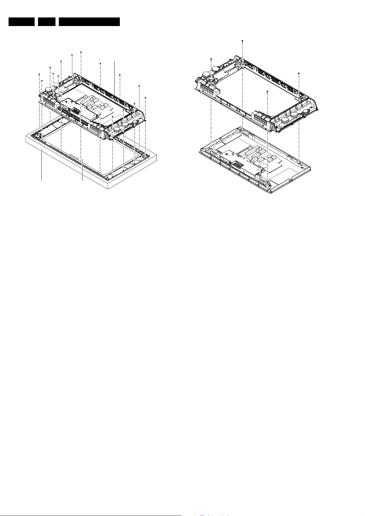
4.4 PDP and Glass Plate Replacement
Shielding frame
Front displayFoam cushion
Figure 4-6 Exchange Glass Plate
To exchange the glass plate
1. Take the monitor from its service stand, and put it (face
down) on a soft surface (blanket or foam cushion), to make
sure that you do not damage the front glass plate.
2. Remove the metal back plate as described in paragraph
"Rear Cover Removal".
3. Unscrew all fixation screws of the plastic back cover: four
at the left and right side, three at the bottom and top side.
4. Lift and remove the plastic back cover.
5. Unscrew two fixation screws of the triangular shaped cable
holder at the left bottom, see figure "Exchange Glass
Plate".
6. Unscrew all fixation screws of the (metallised) shielding
frame, four at both sides and four at the top and bottom,
see figure "Exchange Glass Plate".
7. Unplug the cable of the LED/Switch panel, connector 0320.
8. You can now remove the (metallised) shielding frame,
together with the PDP, Audio panel, Power supply and
SCAVIO panel attached to it, see figure "Exchange Glass
Plate".
Note: To prevent scratches, make sure to put the shielding
frame together with the PDP on a soft surface.
9. Replace the glass plate.
Mechanical Instructions
CL 36532011_013.eps
060303
4.5 Re-assembly
CL 36532011_014.eps
060303
Figure 4-7 Exchange PDP
To exchange the PDP panel:
1. Take out the SCAVIO panel and Power Supply panel.
2. Unscrew all fixation screws of the (metallised) shielding
frame (two at the top and two at the bottom, see figure
"Exchange PDP").
3. Replace the PDP.
To re-assemble the whole set, do all processes in reverse
order.
Notes:
• You must replace the speaker-box sealing foam, in case
the plastic rear cover has been (re)moved.
• While re-assembling, make sure all the cables are in their
original position and make sure all the EMC foams are
present to ensure "EMC tightness".
Page 13
Service Modes, Error Codes and Fault Finding
NORMAL OPERATION
(and all other states)
Override software
protections
Ignore all "Service unfriendly" m odes.
Start blinking LED sequence to s how the
error codes according to the blinking LED
procedure.
Lineair audio and video settings are set to
50% (middle value) except volume (set to
low volume level, 25% of max)
"UNDO" ignore all
"Service unfriendly
modes"
STANDBY
Service Default Mode
Display SDM in "top line"
(all other OSD off).
Blinking LED sequence.
OFF
SAM
Short SDM pins
(also works from Standby)
RC sequence
"00" or
"Standby"
Reset to last status
RC button.
Mains OFF
Mains ON
RC sequence
"0-6-2-5-9-6-MENU"
RC-code
0-6-2-5-9-6-OSD
or INFO+
RC-code
0-6-2-5-9-6-menu
Normal
operation
CL 16532099_100.pdf
260901
5. Service Modes, Error Codes and Fault Finding
Index of this chapter:
1. Test points
2. Service Modes
3. Problems and Solving Tips (related to CSM)
4. ComPair
5. Error Codes
6. The Blinking LED Procedure
7. Protections
8. Repair Tips
5.1 Test Points
The chassis is equipped with test points (I- and F-points)
printed on the circuit board assemblies. See test point
overviews in section “Block Diagrams”
Perform measurements under the following conditions:
• Service Default Mode.
• Video: colour bar signal (via PC or VGA-generator).
• Audio: 1 kHz, 2 V
5.2 Service Modes
(via PC or VGA-generator).
PP
EN 13FM242 AB 5.
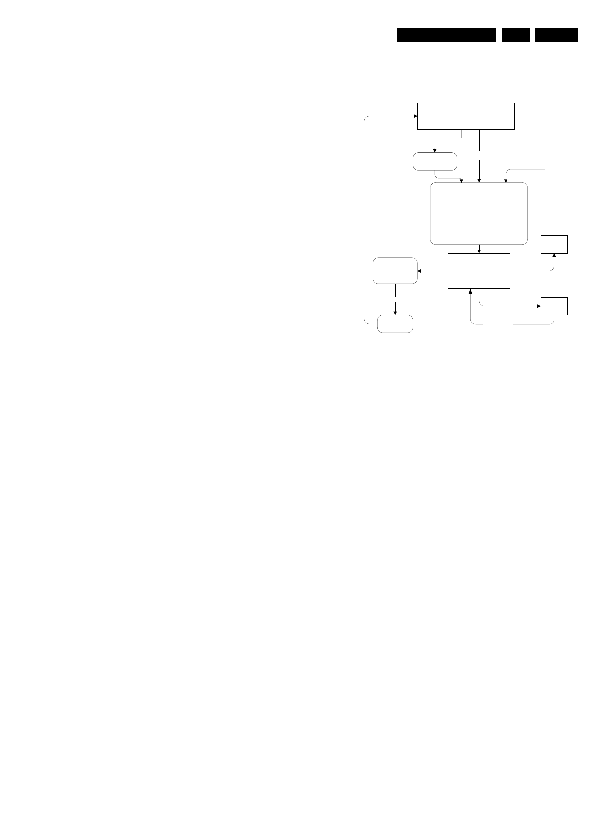
5.2.1 Service Default Mode (SDM)
Service Default Mode (SDM) and Service Alignment Mode
(SAM) offer several features for the service technician, while
the Customer Service Mode (CSM) is used for communication
between a Philips Customer Care Centre (P3C) and a
customer.
There is also the option of using ComPair, a hardware interface
between a computer (see requirements) and the FTV chassis.
It offers the ability of structured trouble shooting, test pattern
generation, error code reading, software version readout and
software upgrading.
Minimum requirements: a Pentium Processor, Windows 9x/NT/
2000/XP, and a CD-ROM drive (see also paragraph
“ComPair”).
Note: This FM242-monitor has different as the FM24, not a
internal pdp-testpattern that can be enabled via the SAM-menu
A test pattern however can be generated.
How?
Select via ComPair-tool the right hex-address (sub address
0080 and then PS (Pattern Select) (00 full window black; 01~04
full window white, red, green, blue) and more variants until 17)
It however only works when set is signalled (Scavio and pdp,
needs a sync). This is less nice solution as in FM24.
Switch of the pattern again via hex-code 0080 and 0.
Purpose
• To create a pre-defined setting to get the same
measurement results as given in this manual.
• To override SW protections (only when SDM is entered via
• To start the blinking LED procedure.
Specifications
• All picture settings at 50% (brightness, contrast, etc.).
• Colour temperature is set to "normal".
• Bass, treble and balance at 50%; volume at 25%.
• All service-unfriendly modes (if present) are disabled, like:
• Video blanking,
• Slow de-mute,
• Anti ageing,
• Automatic switch to Standby when no sync signals are
the "service pins" on connector 0382).
received.
Figure 5-1 SDM Flowchart
How to enter SDM
Use one of the following methods:
• Use the standard RC-transmitter and key in the code
062596, directly followed by the MENU button.
• Short jumpers 1 and 2 of connector 0382 on the SCAVIO
panel.
After entering SDM, a blank screen is visible, with SDM in the
upper left side for recognition. The Blinking LED procedure is
started and will indicate any possible errors via the (orange)
front LED.
How to navigate
To toggle to the SAM mode, use a standard customer RCtransmitter and key in the code 062596, directly followed by the
OSD (i+) key.
How to exit
Use one of the following methods (the set returns to its last
status):
• Switch the set to STANDBY by pressing the power button
on the remote control transmitter (if you switch the set "off"
by removing the Mains power, the set will return in SDM,
when the Mains power is re-applied).
• Use the standard RC-transmitter and key in the code 00.
5.2.2 Service Alignment Mode (SAM)
Purpose
• To perform (software) alignments.
• Easy way to identify the commercial type number of the
set.
• Easy identification of the used software versions.
• To display (or clear) the error code buffer.
• View operational hours.
Specifications
• Operation hours counter.
• Software version reading.
• Error buffer reading and erasing.
• Software alignments.
Page 14
EN 14 FM242 AB5.
RC button,
e.g. P+ or P-
STANDBY
Do not store
settings made
during alignments
RC button,
e.g. P+ or P-
"UNDO" ignore
all "Service
unfriendly
modes"
"Standby"
Settings made
during alignments
are stored
STANDBY
NORMAL OPERATION
RC sequence "0-6-2-5-9-6-OSD "(for Europe & A/P)
RC sequence "0-6-2-5-9-6-INFO+" (for USA/LatAm)
Short SAM pins (works also from Standby)
RC sequence
"00"
or
or
Ignore all "Ser vice
unfriendly" mod es
Service Alignment Mode
Display "SAM" top level
menu
Upper menu selection
(with cursor buttons)
Lower menu selection
(with cursor buttons)
RC-code "0-6-2-5-9-6-OSD"
RC-code "0-6-2-5-9-6-INFO+"
RC-code "0-6-2-5-9-6-MENU" -
Service Modes, Error Codes and Fault Finding
Mains ON
OFF
(Settings made
during alignments
are stored)
Mains OFF
or
SAM submenus
(whitepoints, align-
ments, etc.)
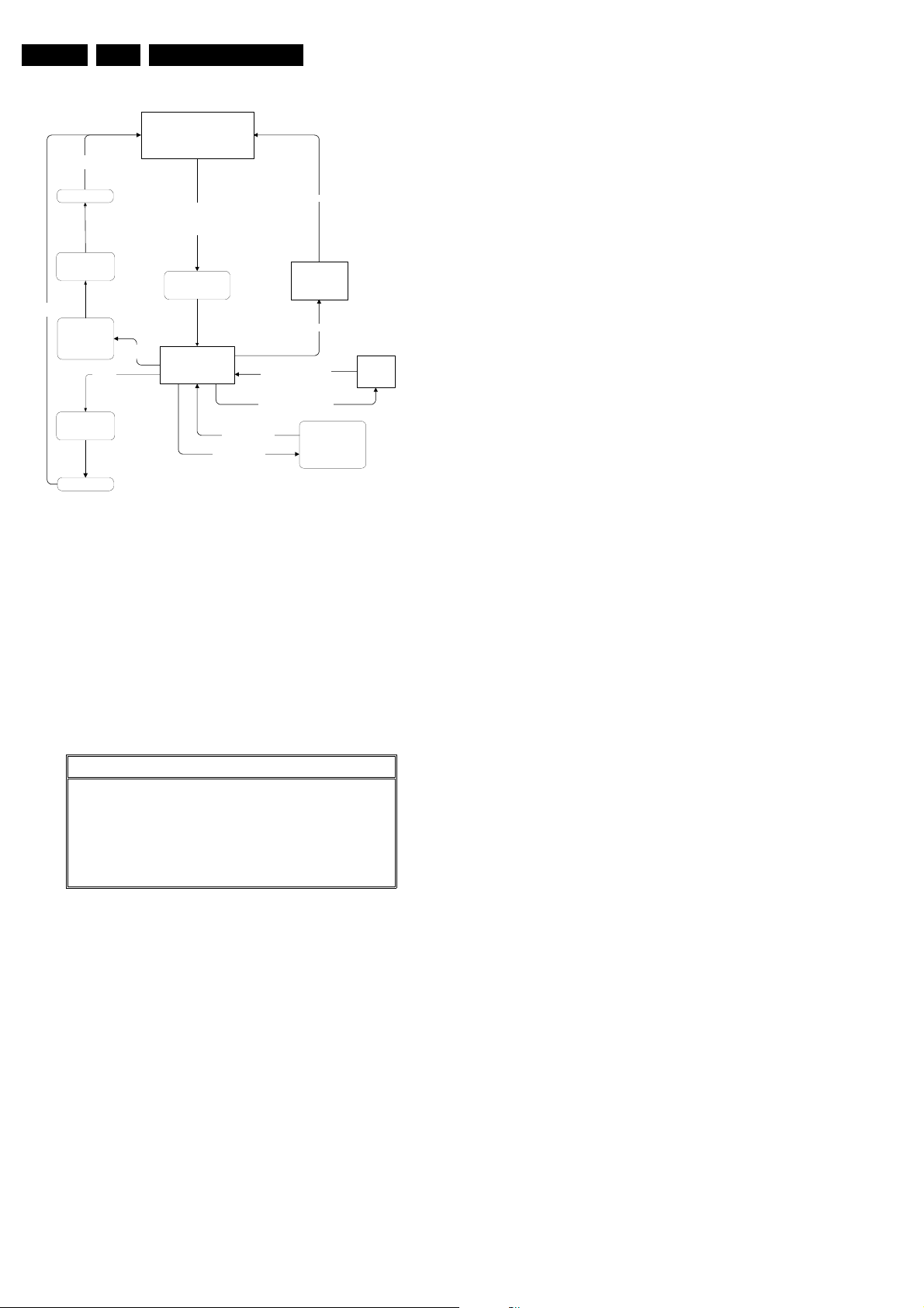
Figure 5-2 SAM Flowchart
How to enter
Use one of the following methods:
• Use a standard RC-transmitter and key in the code 062596
directly followed by the OSD (i+) button
Note: the OSD (i+) is not available on the original FM242
remote control, therefore use another Philips remote
control (e.g. MG, EMG or A10).
• Short jumpers 3 and 4 of connector 0382 on the SCAVIO
panel.
The following screen is visible:
Service Alignment Menu General
Type Nr. - AG Code 42FD9945/01 **00 00
SW Version OTC AAAAAB-X.Y_xxxxx
SW Version PW AAAABC-X.Y_xxxxx
SW Version EPLD AAAABC-X.Y_xxxxx
Operational hours xx
Errors 1 xx xx xx xx xx
Errors 2 xx xx xx xx xx
Reset error buffer Press OK to reset
Store Press OK to store
CL 26532011_016.eps
SDM
CL 16532099_101.pdf
260901
200303
4. SW Version PW (AAAABC-X.Y-xxxxx). See description
above.
5. SW Version EPLD (AAAABC-X.Y-xxxxx). See description
above.
6. Errors 1. Gives the last five errors of the error buffer. The
last detected error is displayed at the most left position.
The errors are displayed as 2 digit numbers and separated
by a space. When less than 10 errors occurred, the rest of
the line(s) is empty. In case of no errors the text "No Errors"
is displayed behind menu item "Errors 1". See paragraph
5.5 for a description.
7. Errors 2. Gives the first five errors of the error buffer. The
last detected error is displayed at the most left position.
8. Operational hours. The Operations Hours indicate the
time that the display was active with half an hour resolution.
It represents the system hours (OTC), not the PDP hours.
9. Reset error buffer. Erase the contents of the error buffer.
Press "OK" on your remote control to activate. The content
of the error buffer is cleared.
10. Store. This will store the performed alignments. Press
"OK" on your remote control to activate.
Note: if you do not want to store the performed alignments,
leave the SAM mode via code 00 on your remote control.
Do not activate the "store" item.
How to navigate
Use one of the following methods:
• Select the sub-menu"s (upper line) with the CURSOR
LEFT/RIGHT keys on the remote control transmitter.
• Select the menu items with the CURSOR UP/DOWN keys.
With the CURSOR LEFT/RIGHT keys it is possible to:
– Activate the selected menu item.
– Change the value of the selected menu item.
• To toggle to the SDM mode, use the standard customer
RC-transmitter and key in the code 062596, directly
followed by the MENU key.
How to exit
Use one of the following methods:
• Switch the set "off" (with the Mains switch or by pulling the
Mains cord).
Note: new alignment settings are always stored, even
when item "store" was not activated!
• Switch the set to "standby" by pressing the power button on
the remote control transmitter.
Note: new alignment settings are always stored, even
when item "store" was not activated!
• Use the standard RC-transmitter and key in the code 0 0.
Note: new alignment settings are not stored (except when
item "store" was activated)!
5.2.3 Customer Service Mode (CSM)
Figure 5-3 SAM Menu "General"
1. Type Nr. Gives the commercial type number of the
monitor, e.g. 42FD9945/01.
2. AG Code. Is not implemented.
3. SW Version OTC (AAAAAB-X.Y-xxxxx).
Note: You will find details of the latest software versions in
the chapter "Software Survey" of the "Product Survey Colour Television" publication, which is published four
times each year.
• A = the chassis name (FM23 for 32" displays or FM242
for 42" SDI-displays).
• B = the region (E= Europe, A= Asia Pacific, U= NAFTA,
L= LATAM; in our case G = Global).
• (if valid) C = the configuration name (B= Basic, E=
Enhanced; for PW & EPLD-software this will be named
B).
• X = the main software version number.
• Y = the sub software version number.
• x = last five digits of 12nc code.
Purpose
When a customer is having problems with his TV-set, he can
call his dealer or helpdesk. The service technician can than ask
the customer to activate the CSM, in order to identify the status
of the set. Now, the service technician can judge the severe
ness of the complaint. In many cases, he can advise the
customer how to solve the problem, or he can decide if it is
necessary to visit the customer.
The CSM is a read only mode, therefore modifications in this
mode are not possible.
Page 15
Service Modes, Error Codes and Fault Finding
Normal operati on mode
Key in sequence: 1-2-3-6-5-4 on RC
Store current picture, sound and feature settings for later
retrieval (only store if needed to go back to normal
operation).
Set pre-defined picture, sound and feature settings (to be
able to see and hear if the set is working pr operly and to be
able to read the CSM information).
Ignore service unfriendly options
Volume up/down
Numerical key,
external
If other key
= standby
"Cursor right"
To previous CSM page
Restore picture, sound and
feature settings (that were
stored during entry)
Display CSM information screen
"Cursor left"
Other key,
e.g. "menu"
mains off
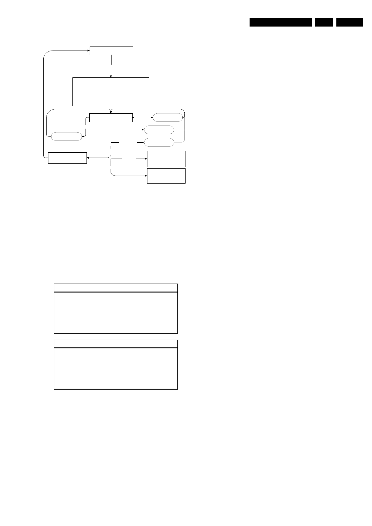
Figure 5-4 CSM Flowchart
How to enter
Use the standard customer RC-transmitter and key in the code
123654.
When CSM is entered, the values of brightness, contrast, etc.
are set to 50% (of max. value), and volume is set to 25%, to
ensure that you always have a picture and sound.
After switching "on" the Customer Service Mode, the following
screen will appear:
Customer Service Menu 1
1 - Type Nr. - AG Code 42FD9945/01
2 - SW Version OTC AAAAAB-X.Y_xxxxx
3 - SW Version PW AAAABC-X.Y_xxxxx
4 - SW Version EPLD AAAABC-X.Y_xxxxx
5 - Code 1 xx xx xx xx xx
6 - Code 2 xx xx xx xx xx
7 - Volume xx
8 - Brightness xx
9 - Contrast xx
Customer Service Menu 2
10 - Colour xx
11 - Tint xx
12 - Sharpness xx
13 - Soundmode xx
14 - Source xx
15 - AV Mute xx
Figure 5-5 CSM Menu
To next CSM page
Increase/decrease
volume
Switch to prese t/
channel or external
Standby
(when the set is switched on,
picture, sound and feature
settings (that were stored
during entry) are restored)
Off
(when the set is switched on,
picture, sound and feature
settings (that were stored
during entry) are restored)
CL 16532099_103.pdf
CL 36532011_015.eps
200303
260901
EN 15FM242 AB 5.
• (if valid) C = the configuration name (B= Basic, E=
Enhanced).
• X = the main software version number.
• Y = the sub software version number.
• x = last five digits of 12nc code.
3. SW Version PW (AAAABC-X.Y-xxxxx). See description
above.
4. SW Version EPLD (AAAABC-X.Y-xxxxx). See description
above.
5. Code 1. Gives the last five errors of the error buffer. The
last detected error is displayed at the most left position.
The errors are displayed as 2 digit numbers and separated
by a space. When less than 10 errors occurred, the rest of
the line(s) is empty. In case of no errors, the text "No
Errors" is displayed behind menu item "Code 1". See
paragraph “Error Buffer” for a description.
6. Code 2. Gives the first five errors of the error buffer. The
last detected error is displayed at the most left position.
7. Volume. Gives the last volume status for the selected
source, as set by the customer.
8. Brightness. Gives the last brightness status for the
selected source, as set by the customer.
9. Contrast. Gives the last contrast status for the selected
source, as set by the customer.
10. Colour (not present in Basic configuration). Gives the last
colour status for the selected source, as set by the
customer.
11. Tint (only for NTSC Enhanced configuration). Gives the
last tint status for the selected source, as set by the
customer.
12. Sharpness. Gives the last sharpness status for the
selected source, as set by the customer.
13. Source. Gives the selected source, as set by the
customer.
14. AV Mute. Indicates if AV Mute is "on" or "off".
How to navigate
Use one of the following methods:
• Switch to the other CSM page with the CURSOR LEFT/
RIGHT keys on the remote control.
• You can increase/decrease volume with the VOLUME UP/
DOWN keys on the remote control.
• You can switch to another source with the NUM/EXT keys
on the remote control.
How to exit
Use one of the following methods:
• Press the MENU key of the remote control transmitter.
• Switch the set to "standby" with the Power switch on the
remote control.
• Switch the set "off" with the Mains power switch.
5.3 Problems and Solving Tips (Related to CSM)
5.3.1 Picture Problems
Note: Below described problems are all related to the monitor
settings. The procedures to change the value (or status) of the
different settings are described.
1. Type Nr. AG Code. Gives the commercial type number of
the monitor, e.g. 42FD9945/01. AG Code is not
implemented.
2. SW Version OTC (AAAAAB-X.Y-xxxxx) Note: You will find
details of the latest software versions in the chapter
"Software Survey" of the "Product Survey - Colour
Television" publication, which is published four times each
year.
• A = the chassis name (FM23 for 32" displays or FM242
for 42" SDI-displays).
• B = the region (E= Europe, A= Asia Pacific, U= NAFTA,
L= LATAM or G = Global).
Picture too dark or too bright
Increase/decrease the BRIGHTNESS and/or the CONTRAST
value when the picture improves after you have switched on
the Customer Service Mode. The new value is automatically
stored.
White line around picture elements and text
Decrease the SHARPNESS value when the picture improves
after you have switched on the Customer Service Mode. The
new value is automatically stored.
Snowy picture and/or unstable picture
A scrambled or decoded signal is received.
Page 16

EN 16 FM242 AB5.
Service Modes, Error Codes and Fault Finding
Black and white picture
Increase the COLOUR value when the picture improves after
you have switched on the Customer Service Mode. The new
value is automatically stored.
Menu text not sharp enough
Decrease the CONTRAST value when the picture improves
after you have switched on the Customer Service Mode. The
new value is automatically stored.
5.3.2 Sound Problems
(if valid, related to speaker-version yes or no)
No sound from left or right speaker
Check item "Volume" in the CSM mode. If value is low,
increase the volume level. The new value is automatically
stored.
No sound or sound too loud (after channel change/ switching on)
Increase/decrease the VOLUME level when the volume is OK
after you switched on the CSM. The new value is automatically
stored.
5.4 ComPair
5.4.1 Introduction
ComPair (Computer Aided Repair) is a service tool for Philips
Consumer Electronics products. ComPair is a further
development on the European DST (Dealer Service Tool),
which allows faster and more accurate diagnostics. ComPair
has three big advantages:
• ComPair helps you to quickly get an understanding on how
to repair the chassis in a short time by guiding you
systematically through the repair procedures.
• ComPair allows very detailed diagnostics (on I
is therefore capable of accurately indicating problem areas.
You do not have to know anything about I
yourself because ComPair takes care of this.
• ComPair speeds up the repair time since it can
automatically communicate with the chassis (when the
microprocessor is working) and all repair information is
directly available. When ComPair is installed together with
the SearchMan electronic manual of the defective chassis,
schematics and PWBs are only a mouse click away.
5.4.2 Specifications
ComPair consists of a Windows based faultfinding program,
and an RS232 cable between PC and the (defective) product.
The ComPair faultfinding program is able to determine the
problem of the defective monitor. ComPair can gather
diagnostic information in two ways:
• Automatic (by communication with the monitor): ComPair
can automatically read out the contents of the entire error
buffer. Diagnosis is done on I2C level. ComPair can send
and receive commands to the micro controller of the
monitor, and so can access the I2C bus of the monitor. In
this way, it is possible for ComPair to communicate (read
and write) to devices on the I2C busses of the FTV monitor.
• Manually (by asking questions to you): Automatic
diagnosis is only possible if the micro controller of the
monitor is working correctly and only to a certain extend.
When this is not the case, ComPair will guide you through
the faultfinding tree by asking you questions (e.g. Does the
screen give a picture? Click on the correct answer: YES /
NO) and showing you examples (e.g. Measure test-point
F7 and click on the correct oscillogram you see on the
oscilloscope). You can answer by clicking on a link (e.g.
2
C level) and
2
C commands
text or a waveform picture) that will bring you to the next
step in the faultfinding process.
By a combination of automatic diagnostics and an interactive
question / answer procedure, ComPair will enable you to find
most problems in a fast and effective way.
Beside fault finding, ComPair provides some additional
features like:
• Software upgrading (upload possible to OTC and PW
Scaler).
• Emulation of the (European) Dealer Service Tool (DST).
• If both ComPair and SearchMan (Electronic Service
Manual) are installed, all the schematics and the PWBs of
the set are available by clicking on the appropriate
hyperlink.
Example: Measure the DC-voltage on capacitor C2228
(Schematic/Panel) of the SCAVIO panel. Click on the
"Panel" hyperlink to automatically show the PWB with a
highlighted capacitor C2568. Click on the "Schematic"
hyperlink to automatically show the position of the
highlighted capacitor.
5.4.3 How to Connect
1. First, install the ComPair Browser software on your PC
(read the installation instructions carefully).
2. Connect an RS232 interface cable between a free serial
(COM) port on your PC and the RS232 connector on the
FM242 plasma monitor.
3. Switch the plasma monitor "off" and "on" again (with the
Mains switch).
4. Start the ComPair program and follow the instructions.
Note: once the set is in ComPair mode, the front LED will blink
red, at a frequency of 0.3 Hz.
5.4.4 How to Order
ComPair order codes:
• Starter kit ComPair32 software (registration version): 3122
785 60040.
• ComPair32 CD (update): 3122 785 60070.
• Starter kit SearchMan32 software: 3122 785 60050.
• SearchMan32 CD (update): 3122 785 60080.
Note: The RS232 cable is not included. It is a standard cable
(9p sub-D male-to-female) that can be obtained by a computer
store. It is supplied however with the ComPair interface (4822
727 21631), necessary for servicing other Philips TVs.
5.5 Error Buffer
The error code buffer contains all detected errors since the last
time the buffer was erased. The buffer is written from left to
right. When an error occurs that is not yet in the error code
buffer, it is written at the left side and all other errors shift one
position to the right.
5.5.1 How to Read the Error Buffer
Use one of the following methods:
• On screen via the SAM (only if you have a picture).
Examples:
– Errors: 6 0 0 0 0, error code 6 is the last and only
detected error.
– Errors: 9 6 0 0 0, error code 6 was first detected and
error code 9 is the last detected (newest) error.
• Via the blinking LED procedure (when you have no
picture). See paragraph “The blinking led procedure”.
• Via ComPair.
Page 17
Service Modes, Error Codes and Fault Finding
EN 17FM242 AB 5.
5.5.2 How to Clear the Error Buffer
The error code buffer is cleared in the following cases:
• By activation of the "Reset error buffer" command in the
SAM menu.
• When you transmit the code 062599 with a standard
remote control transmitter.
5.5.3 Error Codes
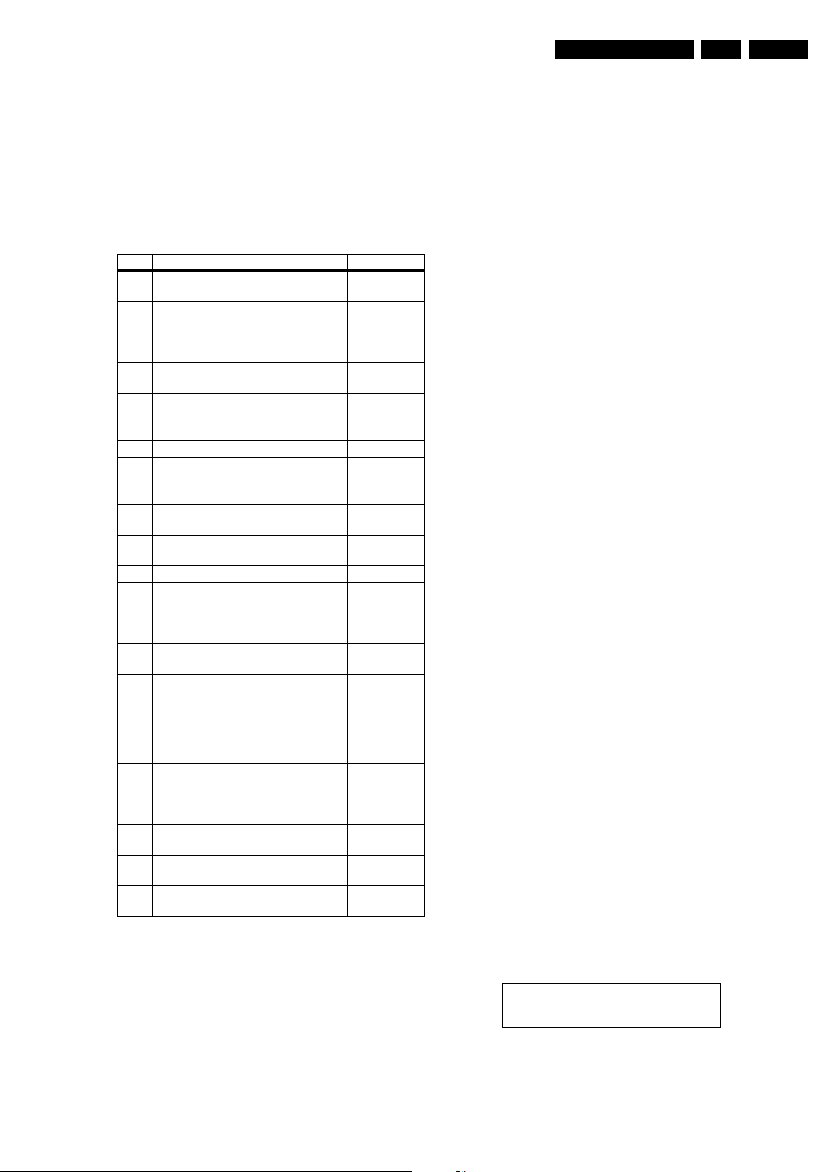
Table 5-1 Error code overview
Error Device Description Item Diagr.
1 TEA6422D Audio switch
(only Enhanced)
2 MSP3451G Sound
processor
3 PCF8574- SCAVIO I/O expander
SCAVIO
4 PCF8591 AD-DA
expander
5 FS6377 Clock generator 7570 SC9
6 PCF8574-PSU I/O expander
PSU
7 24C16 OTC NVM OTC 7430 SC7
8 24C16 PW NVM PW 7580 SC9
9 SAA7118 Video decoder
(only Enhanced)
10 AD9887 ADC/TMDS
receiver
11 SDA9400 De-interlacer
(only Enhanced)
12 EP1K30QC EPLD processor 7656 SC11
13 PDP I2C error of the
PDP
20 Download comm. Errors during
downloading
21 CSP comm. CSP time-out
error
40 Temperature alarm Detections of
over-
temperature
70 Over voltage Vs, Va, +5V,
+3V3
overvoltage
71 Vs under voltage Vs under voltage Black
72 Va under voltage Va under voltage Black
73 +5V under voltage +5V under
voltage
74 +3V3 under voltage +3V3 under
voltage
75 DC-PROT Audio amplifier
protection
Notes:
• In case of non-intermittent faults, clear the error buffer
before you begin the repair. This to ensure that old error
codes are no longer present.
• If possible, check the entire contents of the error buffer. In
some situations, an error code is only the result of another
error code and not the actual cause (e.g., a fault in the
protection detection circuitry can also lead to a protection).
• In case error 70 occurs, the belonging over-voltage line
cause can be located via measuring. (via measuring all 4
voltages simultaneously with an oscilloscope). Chosen
7798 SC13
7812 SC14
7540 SC8
7530 SC8
7370 P3
7225 SC5
7170 SC4
7280 SC5
Black
P
box
P
box
P
box
Black
P
box
Black
P
box
Black
P
box
FM242-workshops will be trained how to do so. (special
document will be generated for this).
5.6 The Blinking LED Procedure
Via this procedure, you can make the contents of the error
buffer visible via the front LED (orange colour).This is
especially useful when there is no picture. When no errors are
present, the LED will stay green.
When the SDM is entered, or when code 062500 is entered
with the remote control, the LED will blink the contents of the
error-buffer.
Error-codes ≥ 10 are shown as follows:
1. n long blinks of 750 ms, which is/are an indication of the
decimal digit,
2. a pause of 1.5 s,
3. n short blinks (n = 1-9),
4. when all the error-codes are displayed, the sequence
finishes with a LED blink of 3 s,
5. the sequence starts again.
Example of error buffer: 12 9 6 0 0
After entering SDM:
1. 1 long blink of 750 ms followed by a pause of 1.5 s,
2. 2 short blinks followed by a pause of 3 s,
3. 9 short blinks followed by a pause of 3 s,
4. 6 short blinks followed by a pause of 3 s,
5. 1 long blink of 3 s to finish the sequence,
6. the sequence starts again.
5.7 Protections
You can read the error codes of the error buffer via the service
menu (SAM), the blinking LED procedure, or via ComPair. If a
fault situation is detected an error code will be generated and if
necessary, the set will be put in the protection mode. Blinking
of the red LED at a frequency of 5 Hz indicates the protection
mode.
In some error cases, the microprocessor does not put the set
in the protection mode. The error codes are indicated by an
orange front LED.
To get a quick diagnosis the chassis has three service modes
implemented:
• The Customer Service Mode (CSM): easy way to read out
the status of the set.
• The Service Default Mode (SDM): start-up of the set in a
predefined way.
• The Service Alignment Mode (SAM): adjustment of the set
via a menu and with the help of test patterns.
Exceptional ‘protection’ situation
There exists one ‘protection’ (due to too high internal settemperature), where the set does not switch to ‘protection’mode but to Standby-mode. This protection is not logged into
the error-buffer.
When the set becomes too warm, an ‘On Screen Display’message will be showed set is going to switch to Standby. After
some time set can be switched on again. (It is very unlikely this
will happen. For that reason this performance has been
accepted).
Temperature error The monitor will switch
to standby automatically. Please allow cool
down.
Page 18

EN 18 FM242 AB5.
5.8 Repair Tips
If one of the errors of the error buffer points to a defective
supply, then the supply-panel must be send for central repair.
If the symptoms (still to be communicated; e.g. when VS-value
is too high some pixels do not extinguish, when VS-value is too
low some pixels do not enlighten) match with a possible
misalignment of a supply-line, this supply-line could be
checked, and re-aligned.
Only do this if there is a slight spec-violation.
In case it does not help, re-align to the previous wrong setting,
to keep cause-image in tact, for central repair workshop.
Replace supply panel by a new one, and match the supply with
the pdp. .
• (See alignment instructions in chapter “Alignments”)
Service Modes, Error Codes and Fault Finding
Page 19
Block Diagrams, Testpoint Overviews, and Wiring Diagram
6. Block Diagrams, Testpoint Overviews, and Wiring Diagram
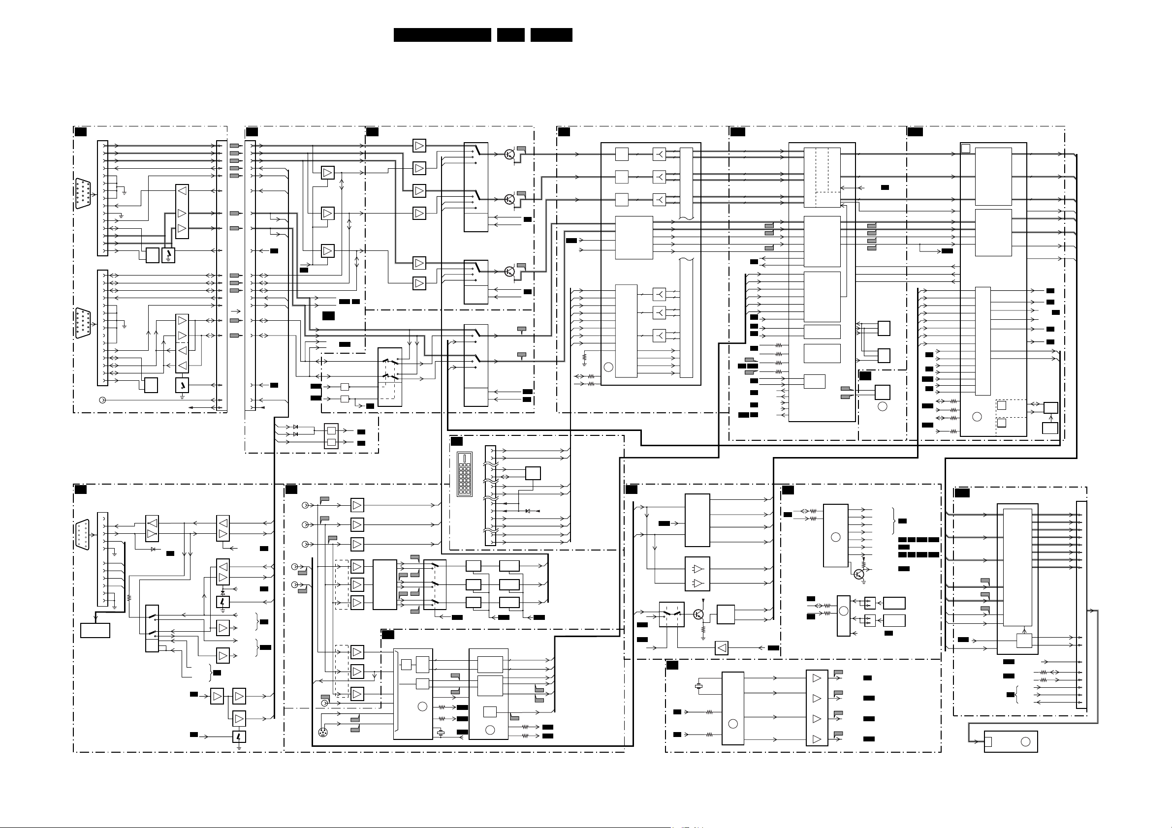
Block Diagram Video
VIDEO
VGA
VGA
CONNECTOR
0371 0318 0318
VGA1-R
1
VGA1-G
2
VGA1-B
3
VGA1-TXD
4
VGA1 IN
15P"D"SHELL
CONNECTOR
5
6
6
1
11
7
2
12
7
8
3
13
9
8
4
14
10
5
15
VGA2
IN/OUT
15P"D"SHELL
CONNECTOR
6
11
1
7
12
2
8
13
3
9
14
4
10
15
5
RC-OUT
SC6
RS-232
IN/OUT
5
10
4
9
3
8
2
7
1
6
BLOCK DIAGRAM
RS 232 INPUT
CONTROL
RC-VGA1
9
10
VGA1-RXD
11
DCC-SDA-1
12
VGA1-H
13
VGA1-V
14
DCC-SCL-1
ST24FC21
VGA2-R
VGA2-G
VGA2-B
VGA2-TXD
VGA2-RXD
DDC-SDA-2
VGA2-H
VGA2-V
DDC-SCL-2
RXD
TXD
5
DDC
7
NVM
7904
DDC
NVM
7907
ST24FC21
+5V-STBY-SW +5V-STBY-SW
7352
ST3232E
11
14
12
13
6366
PS-232-ACT
SC7
3913
7340 A+B
74HC4052D
1
TXD-OTC
3
5
TXD-PW
12
13
14
10
9
LOGIC
6
15
0372
1
2
3
4
5
6
7
8
N.C.
9
10
11
12
13
14
15
0376
1
2
3
RL_ICN
4
5
GL_ICN
6
LD_ICN
7
IR_TX
8
IR_RX
9
10
11
SEE
6
1
13
9
2
11
6
7900
EBOX-PRESENT
10
7937
7940
7910
VGA1-R
VGA1-G
VGA1-B
VGA1-TXD
VGA1-RXD
RC-VGA1
9
VGA1-H
4
VGA1-V
10
VGA2-R
VGA2-G
VGA2-B
VGA2-TXD
VGA2-RXD
VGA2-H
8
VGA2-V
3
12
5
VGA-OUTN
7915
SELECT-3
SELECT-2
SC8
SC7
TXD-2
RXD-2
RC
RC-CONTR
11
9
10,13
3
5
7310
SC8
2
4
6
12
13
15
8
10
29
17
19
21
27
28
23
25
31
30
32
7303 C+D
7303 A+B
1.4
7315, 7316
7325, 7326
SC6
F303
31
F304
29
F305
27
F308
21
F309
20
18
F306
25
F307
23
F311
16
F312
14
F313
12
F314
10
F315
12
VGA2-TXD
8
VGA2-RXD
SELECT-4
26VGA1-RXD
VGA1-TXD
SELECT-1
VGA1-RXD
TXD-OTC
RXD-OTC
TDX-PW
RXD-PW
73237322
RC-OUT
7320
RC-VGA1
7321
VGA
INPUT
VGA1-R
VGA1-G
VGA1-B
VGA1-TXD
VGA1-RXD
RC-VGA1
VGA1-H
VGA1-V
(EBOX-
PRESENT)
SC7
4
TV MODE
VGA2-TXD
6
VGA2-RXD
5
VGA2-H
VGA2-V
8
VGA2OUTN
SC6
2
RC-OUT
3
1
6379
6378
SC3
R/Pr/Cr
G/Y/Y
B/Pb/Cb
SC8
2fh 1fh 2fh
V
H
SC8
SC7
SC10
VGA2OUTN
SC6
SC10
SC10
VGA1-V
VGA1-H
VGA1-RXD
VIDEO SELECTION
& MATRIX
AV3 (HD)
V-HD-EXT
F072
H-HD-EXT
F075
AV1
7311-A
7311-B
7311-C
VGA1-H
VGA1-V
11
F071
F070
Y-H D
F073
251
SVHS
SC2
VGA1-V
VGA1-H
VGA2-V
VGA2-H
VGA2-V
VGA2-H
VGA2-EN
VGA2-OUT
7370 A+B
O.S.
O.S.
F074
AV2
34
SC11
SYNC
SELECTION
SC11
7060
7065
75
9
R
G
B
Pr
Y
Pb
1Fh
Cr
Y
Cb
CVBS
C
Y
VGA2-EN NOT
VGA2-OUTN
SC3
VGA2-R
VGA2-G
VGA2-B
SC7
11-9
SC6
SYNC-ACT
SC7
UART-ACT
SC7
7141
7138
7135
70792Fh
7074
7084
1fh BUFFER
7117
Cr
7113
Ys
7121 Y-HD
Cb
F236
F235
VIDEO SELECTION
7007 A+C
74HCT4053T
14
4
6
LOGIC
7088
7090
RGB
MATRIX
SC5
MATRIX-SEL
8x
8x
H-DEC
V-DEC
clock
PW-SDA
3250
3250
PW-SCL
VGA1-R
VGA2-R
R-2Fh
R-YUV
VGA1-G
VGA2-G
G-2Fh
G-YUV
VGA1-B
VGA2-B
B-2Fh
B-YUV
VGA1-V
VGA2-V
VGA1-H
VGA2-H
SC4
4
15
14
Y-DEC
UV-DEC
F240
F247
1250
VIDCLK
24.576MHz
SC11
V-HD
12,14
H-HD
1,5
SC10
2
4
1
5
15
11
12
14
2
4
1
5
2
4
15
11
SC9
SC9
7146
74HC4052D
LOGIC
7158
74HC4052D
LOGIC
7009
74HC4052D
LOGIC
DVI-D INPUT
7102
CLAMP
7103
CLAMP
7104
CLAMP
7280
SDA 9400
23
22
54
0375
DVI-D INPUT SOCKET
INTERLACER
CLOCK
7145
7148
7151
7154
7157
7160
12
13
5
3
R-2Fh
G-2Fh
B-2Fh
7089
I054
74HCT4053D
R-NTSC
R-ATSC53
I058
I065
G-NTSC
G-ATSC21
I072
I078
B-NTSC
B-ATSC123
I083
VIDE-SELECTION
DECODER
DECODER DE-INTERLACER
7225
SAA7118C
VIDEO
DE-
ADC
CODER
SYNC
CNTRL
P4
ERR
9
10
14
16
17
18
23
24
SYNC
7129
F146
3
7130
F152
13
VIDEO-SEL-1
9
10
3
9
10
3
13
9
10
1
2
6
7
9
DE-
ERR
11
VIDEO-SEL-2
7131
VIDEO-SEL-1
VIDEO-SEL-2
V-ADC
H-ADC
SYNC-SEL
VIDEO-SEL-2
7100-B
BLANKING
7100-C
BLANKING
7100-A
BLANKING
SC11
HD-CLAMPN
SC8
F158
SC8
F211
F210
SC10
SC8
SCL
DDC
SDA65
EPROM
6210
R-YUV
G-YUV
B-YUV
8x8xY-OUT
UV-OUT
61
V OUT-DEINT
60 H OUT-DEINT
62
V PEN
CLKOUT-DEINT
26
F249
PW-SDA
3284
21
3285
20
PW-SCL
19FM242 AB 6.
SC11
HD-BLANKN
F246
F245
SC10
SC10
SC4
RX2-
RX2+
7215
ST24FC21
RX1-
RX1+
+5V-STBY-SW
RXD-
RXD+
RXC+
RXC-
VIDEO SELECTION - ADC
119R-ADC
110G-ADC
100B-ADC
GBLKSPL
SC10
GCOAST
RXO+
RXO-
RX1+
RX1-
RX2+
RX2-
RXC+
RXC-
PW-SDA
3209
PW-SCL
3210
7170
AD9887KS
81V-ADC
82H-ADC
93
94
62
63
59
60
56
57
65
66
53RTHERM DATACK
ERR
92
91
ADC-TMDS PW EPLD
8x
ADC
8x
ADC
8x
ADC
SYNC. PROC
+
CLOCK
GENERATION
8x
8x
TMDS
RECEIVER
8x
DE
SC2
H-SYNC
V-SYNC
SYNC SELECTION
& SWITCHING
Y-H D
C-SYNC-OUT
SC11
SC11
H-PRESNT
10
H-HD-EXT
2
1
8x
8x
8x
8x
8x
8x
8x
8x
8x
8x
8x
8x
V-HD-EXT
75 OHM-ON
SC11
7007-B
74HCT4053D
10 6
SC9
MUXES
7000 - 7002
7006 - 7010
PROCESSING
7025 A-B
LM319D
COMPARATOR
10
5
15
VGA2-EN-NOT
SCALER - CLOCK
GENERATOR
24.576 MHz
SC7
SC7
V-SYNC
H-SYNC
+
-
+
-
SDA-1
SCL-1
SCALER-PW164-MEMORY
SC10
8x GRE (0-7)
8x GRO (0-7)
8x GGE (0-7)
8x GGO (0-7)
8x GBE (0-7)
8x GBO (0-7)
138
139
140
134
137
7
12
+5B
7040
LM 1881M
2
3051
7060
3571
3570
16
SYNC
SLICER
7570
FS6377
5
6
GENERATOR
1
CLOCK
ERR
SC5
SC11
V-SYNC-TTL
V-SYNC-POL-N
H-SYNC-TTL
H-SYNC-POL-N
V-SYNC-CMP
H-SYNC-CMP
C-SYNC-LM
1
V-SYNC-LM
3
VGA2-EN
5
ADVS
ADHS
ADSOG
GCLK
ADDE
F615
F616
15
13
12
10
SC11
SC4
SC7
SC7
SC9
SC7
SC6
SC2
SC8
SC3
F619
F633
F618
CLKOUT-DEINT
8x UV-OUT
VOUT-DEINT
HOUT-DEINT
PW-START
PW-PRESET
SDA-2
SCL-2
PW-SDA
PW-SCL
RXD-PW
TXD-PW
VGA2-OUT
VGA2-EN
VIDEO-SEL-1
VIDEO-SEL-2
SYNC-SEL
SC10
GBLKSPL
GCOAST
8x Y-OUT
VPEN
MCLK
3608
3606
3604
3605
7605
PW164
CONTROL FUNCTIONS
SC8
SDA1
SC7
SCL1
SC7
SDA1
SCL1
SC7
7574
74LVC125A
5
9
GRAPHICS PORT
SYNC
DECODER
AND
TIMER
YUV
TO
RGB
CLOCK
GEN
MICRO-
PROCESSOR
UART
3541
15
14
3540
PIXEL PROC.
VIDEO
PORT
7540
PCF8574A
3532
3531
32
6
8
1112
8x DRE (0-7)
8x DGE (0-7)
SCALER
SC9
DCK EXT
8x DBG (0-7)
PARITY PARITY-OUT
F637
F639
F634
F638
7630
M29W160DT
DATA
FLASH
ADD
ROM
CNTRL
7628
CY62126
DATA
ADD
SRAM
CNTRL
PW-NVM
SC9
7580
M24C32
SDA
EXP.
ERR
10
I/O
3
9
F566
F565
F563
F564
F569
F567
7530
PCF8591
ADC
ERR
4
5
6
7
9
10
11
12
7563
1
4
2
3
VIDCLK
(24.567 MHz)
VXCA
(18.432 MHz)
MCLK
(120 MHz)
DCKEXT
(36 MHz)
5
SCL
6
SELECT-1
SELECT-2
SELECT-3
SELECT-4
VIDEO-SEL-1
POWER-DOWN
VIDEO-SEL-2
3548
MSP-RESET
0315
1
2
0316
1
2
TEMP3-SENSOR
SC5
SC14
AUDIO
SC10
SC10
NVM
ERR
8
TEMPSENSOR S1
(OPTIONAL)
TEMPSENSOR S2
(OPTIONAL)
P3
SC6
SC6
SC12
SC6 SC3
SC14
SC11
SC3
BACK-END-EPLD
DVS
DHS
DEN
DCLK
FBX MODE
1-2 FH
SYNC
SC5
SC6
SC10
SC8
SC10
SC12
SC10 SC11
SC10 SC11
SC12
V-SYNC-TTL
V-SYNC-POL-N
H-SYNC-TTL
H-SYNC-POL
C-SYNC-LM
V-SYNC-LM
V-SYNC-COMP
H-SYNC-COMP
VGA1-V
VGA1-H
VGA2-V
VGA2-H
SYNC-SEL
VIDEO-SEL-1
VIDEO-SEL-2
PW-SDA
PW-SCL
SDA-1-3V3
3664
SCL-1-3V3
3662
7656-A+B+C
EP1K30FC256
A
SC12
8x R-OUT (0-7)
8x G-OUT (0-7)
8x B-OUT (0-7)
V-SYNC-OUT
H-SYNC-OUT
BLANK-OUT
PARITY-OUT
SC10
PWDWN--LVDS
DIGITAL
CONTRAST
SYNC
DELAY
SYNC
PROC.
ERR
12
BACK-END-LVDS OUTP
7670
DS90CC385M
50-56
2-4
6-8
10-15
16,18-20
22-25
F619
28
F690
27
F692
30
25
DCLK
31
32
B
CONTROLS
C
SUPPLY
& GROUND
SC12
SC12
PLASMA
DISPLAY
PANEL
LVDS
TTL PARALLEL
TO
LVDS
(LVDS
ENCODER)
TTL
LVDS
POWER DOWN
SDA-1-3V3
SCL-1-3V3
PDP-GO
SC7
CPU-GO
IRQ-PDP
PDP
8x R-OUT (0-7)
8x G-OUT (0-7)
8x B-OUT (0-7)
V-SYNC-OUT
H-SYNC-OUT
BLANK-OUT
PWRDWN-LVDS
75 OHM-ON
SC2
H-PRESENT
SC2
HD_BLANKN
HD_CLAMPN
C-SYNC-OUT
SC2
TV MODE
SC6
V-HD
H-HD
7655
EPC2
DATA
CNTRL
PROM
585
PROG
SOCKET
TX OUT0-M
48
TX OUT0-P
47
TX OUT1-M
46
TX OUT1-P
45
TX OUT2-M
42
TX OUT2-P
41
TX OUT3-M
38
TX OUT3-P
37
3837TX CLK OUT-M
TX CLK OUT-P
3680
3684
ERR
30
CL 26532038_001.eps
SC3
PDP
INTERFACE
CONNECTOR
PDP-GO
CPU-GO
IRQ-PDP
0318
19
17
15
13
11
9
3
1
7
5
4
14
18
8
10
6
150402
Page 20
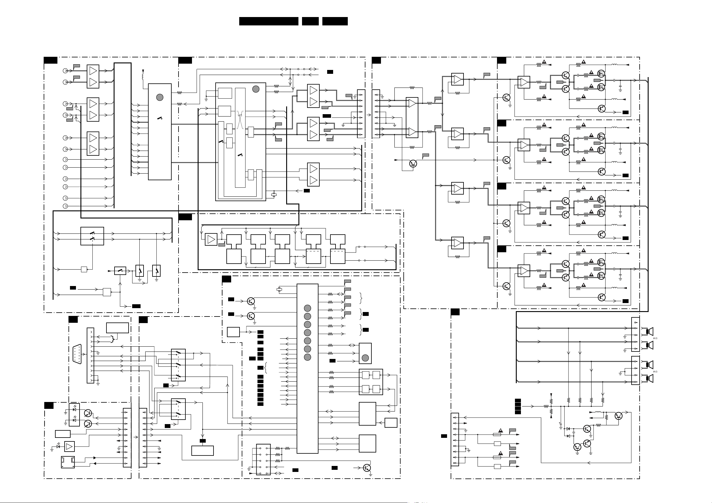
Block Diagrams, Testpoint Overviews, and Wiring Diagram
Block Diagram Audio
20FM242 AB 6.
AUDIO
AUDIO SOURCE
SC13
SELECT
L
AUDIO
VGA IN
R
L
AUDIO
FLEX
VGA
R
L
AUDIO
DVI-D
R
L
AV1
AUDIO
CVBS
R
L
AV2
AUDIO
YC
R
AV3
L
AUDIO
RGB
YPbPr
R
YCbPr
SC1-L
SC1-R
D-CTR-NIL
D-CTR-ONE
CONTROL
LED
LD
PANEL
7107
RC
RECEIVER
2
6127
1101
4
ON/OFF
5
SWITCH
6
7120
F713
F714
1
4
SC8
SC6
GREEN
RED
F710
F711
RS-232
IN/OUT
2
6
2
A
6
B
2
6
7800 A+B
74HC4053D
2
12
7718
POWER-OK
RS232 INPUT
5
10
4
9
3
8
2
7
1
6
6103
2
3
7
1
2
3
7714
LM833D
7734
LM833D
7754
LM833D
0376
1
2
3
4
5
6
7
8
9
10
11
10,11
7103
7105
1
7
1
7
1
7
15
14
ANTI PLOP
+9V-STBY
7801
7802
BLOCK DIAGRAM
RXD
TXD
RL_ICN
GL_ICN
LD_ICN
IR_TX
IR_RX
GREEN-LED
RED-LED
RC-IN
LIGHT-SENSOR-IN
+8V6
+5V-STBY-SW
+9V-STBY-SW
+9V-STBY
L4
R4
L5
R5
L6
R6
L2
R2
L3
R3
L1
R1
7803
SEE
VIDEO
N.C.
L1
L2
L3
L4
L5
L6
R1
R2
R3
R4
R5
R6
7805
7806
AUDIO-ENABLE
SC14
0320
1
2
3
4
5
6
7
8
9
10
5798
+8V6
SC8
0320
1
2
3
4
5
6
7
8
9
10
10
11
25
24
23
20
19
18
7798
TEA6422D
3
ERR
4
5
6
9
MATRIX
SWITCH
7807
7808
CONTROL
FUNCTIONS 2
ICON_NOT
1
LD_ICN
GL_ICN
RL_ICN
SC7
IR_TX
IR_RX
ICON_NOT
SC7
+8V6
+5V-STBY-SW
+9V-STBY-SW
+9V-STBY
SC14
3795
28 SDA-AUDIO
3794
27
12 PRE-OUT1-L
13
PRE-OUT1-R
SC15
AUDIO
DELAY LINE
A
B
7555
74HC4053D
2
1
12
13
5
3
7550
74HC4053D
2
1
12
13
AUDIO-PROCESSOR
SCL-AUDIO
GREEN_LED
15
14
RED_LED
4
15
14
BLOCK DIAGRAM
RC
I2SDATA-IN1
I2SDATA-IN2
SC6
SEE
VIDEO
B
7879
TC74HC590AF
RC
7812
MSP3415G
3
2
17
21
40
41
DEMO-
DULATOR
PRE-
SCALE
DAC
DIGITAL
DAC
SOUND
7874
TC74HC590AF
F872
CONTROL FUNCTIONS 1
SC7
SC6
SC6
7517
ADM 810
RESET
DSP
PROC.
VGA1-H
VGA1-V
2
ERR
2
I2S-DATA-OUT
I2S-CLOCK
DACM-L
DAC
DACM-R
DAC
7870
TC74HC590AF
7432
7433
RESET
SC13
SERVICE PINS
1
3
5
7
9
+5V
SDA-AUDIO
SCL-AUDIO
13
12
16
14
27
26
8
9
3130L
R
5 18.432 MHz VXCA
6
7x
OTC-H
RESET
SC7
SC10
PW_FLASH_RESET
ICONN_NOT
SC8
STANDBY
SC8
SC10
PW-START
SC8
POWER-OK
CPU-GO
PDP-GO
SC12
IRQ-PDP
SC6
RC-CNTL
SC10
PW-RESET
SC10
PW-START
SC8
FAN-SP2
SC8
FAN-SP1
SC6
UART-ACT
SC6
SYNC-ACT
GND-LED
RED-LED
RC
LIGHT-SEN-IN
0382
SDM
4810
4811
7841
3813
3812
A
B
I660
I659
LM833D
3
6
7851
LM833D
3
6
7861
TS462CD
2
6
SC9
AUDIO DELAY PROC.
A
7880
CY7C199B
7x
RAMCOUNTER COUNTER "D" F.F. "D" F.F.
1415
6MHz
SERVICE-IN
3419
2
3380-C
3422
4SAM
3421
6CMP
8
SCL-1
10
SDA-1
16
17
83
84OTC-V
74
109
120
119
95
96
116
115
93
110
108
95
104
103
99
98
114
113
100
105
106
SC7
7x8x
7383
SAA5801H
7881
74HCT573
8x
FRAME
OTC
ERR
91
ERR
92
ERR
93
ERR
94
ERR
95
ERR
96
ERR
97
SDA-1
SCL-1
1
7
1
7
1
7
82
86
85
88
87
89
90
91
92
43
42
40
41
F813
SC13
F816
8x
SC7
AUDIO-ENABLE
F817
7882
74HCT573
3404-C
3404-D
3404-A
3404-B
3402-D
3402-C
3402-B
3402-A
SC7
3464-D
3464-C
3464-A
3464-B
SC6
F812
L-POS
L-NEG
D-CTR-ONE
D-CTR-NIL
SC1-L
SC1-R
17
15
F383
F427
F428
F425
F426
SDA-NVM-1
SCL-NVM-1
RESET
ROM-CS
RAM-CS
ROM-OE
RAM-OE
DATA
ADDRESS
CONTROL
DATA
ADDRESS
CONTROL
RS_232_ACT
R-POS
R-NEG
SDA-1
SCL-1
SDA-2
SCL-2
RXD-OTC
TXD-OTC
0388
7
6
5
4
3
2
1
4884
24 ms MONITOR
4894
40 ms TV
SEE
IIC DIAGRAM
SC10
SC6
7430
MC24C32
5
6
NVM
ERR
7
7
7510 - 74 LVCOOAD
1
2
9
10
7506
AM29DL164DT
DUAL
BANK
FLASH
ROM
7500
MSM51V18165F
DRAM
A2
0388
7435
FILTERS
88
7
6
5
4
3
2
1
+9V-STBY A
I2S-DATA-IN1
I2S-DATA-IN2
26
28
12
L-POS
L-NEG
AUDIO-ENABLE
R-POS
L-NEG
CS
6
OE
11
CS
OE
7515,7516
FLASH
RESET
7225
LM833DT
3
2
5
6
3207
3222
7211
BC857BM
AUDIO
A3
AMPL-
1730
2.5A
7735,7736
STAB
1740
2.5A
7745,7746
STAB
A4
A5
A6
7302
7402
7502
7602
L-HIGH
AUDIO
AMPLL-LOW
AUDIO
AMPLR-HIGH
AUDIO
AMPLR-LOW
F730
F735
F740
F745
7315
LM311D
2
3
7415
LM311D
2
3
7515
LM311D
2
3
7615
LM311D
2
3
A3
A4
A5
A6
7260-A
LM833DT
3
1
2
3259
F231
3220
1
7238-A
LM833DT
F241
3240
7
F211
TO
0302
P6
POWER
SUPPLY
3
1
2
3234
7260-B
LM833DT
5
7
6
3274
7238-B
LM833DT
5
7
6
3244
SUPPLY & DC PROTECTION
A7
0302
9
8
7
6
5
4
3
2
1
L-HIGH
L-LOW
AU-EN-NOT
R-HIGH
L-HIGH
DC-PROT
+9V-STBY
F258
F235
F273
F245
8
1,4
8
1,4
8
1,4
8
1,4
OUT_PROT
VSDN-POS
VCC-10-POS
VSDN-NEG
VCC-10 -NEG
7
7
7
7
3315
3328
F328
3318
3415
3428
F428
3418
3515
3528
F528
3518
3615
3628
F628
3618
OUT_LH
OUT_LL
OUT_RH
OUT_RL
VCC-10-POS
VCC-10-NEG
VCC-10-POS
VCC-10-NEG
VCC-10-POS
VCC-10-NEG
VCC-10-POS
VCC-10-NEG
VCC_10_POS
3749
VCC_10_NEG
F330
F430
F530
F630
3755
3765
2760
3330
7330
2330
2355
7355
3355
3430
7430
2430
2455
7455
3455
3530
7530
2530
2555
7555
3555
3630
7630
2630
2655
7655
3655
3770 3771 3780
+9V-STBY
+9V-STBY A
6750
2759
6760
7755
3337
3362
3437
3462
3537
3552
3637
3662
7751
7365-2
IRF7343
G
F365
G
7365-1
IRF7343
7465-2
IRF7343
G
F465
G
7465-1
IRF7343
7565-2
IRF7343
G
F565
G
7565-1
IRF7343
7665-2
IRF7345
G
F665
G
7665-1
IRF7345
5753
3751
7761
DC-PROT
5335
D
S
D
S
7340
D
S
D
S
7440
D
S
D
S
7540
D
S
D
S
7640
3781
CL 26532038_002.eps
VSDN-POS
5365
2355
5366
VSDN-NEG
OUT_PROT
A7
5435
VSDN-POS
5465
2465
5460
VSDN-NEG
OUT_PROT
A7
5535
VSDN-POS
5565
2565
5560
VSDN-NEG
OUT_PROT
A7
5335
VSDN-POS
5665
2665
5660
VSDN-NEG
OUT_PROT
A7
DC-PROTECT
7753
BC857BW
3752
150402
OUT_LH
OUT_LL
OUT_RH
OUT_RL
0303
0304
5
L-HIGH
4
3
2
1
L-LOW
R-HIGH
4
3
2
1
R-LOW
Page 21
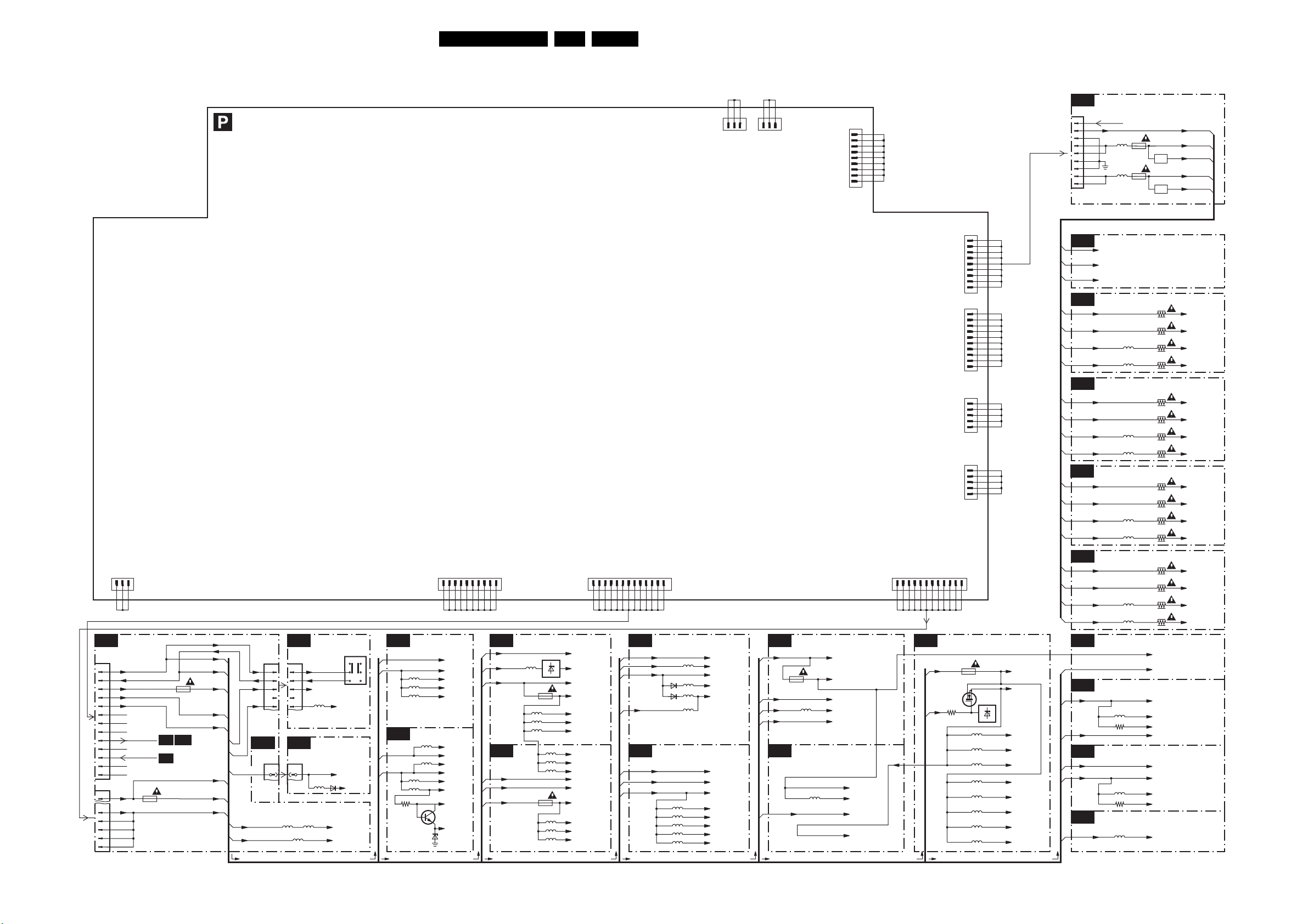
Block Diagrams, Testpoint Overviews, and Wiring Diagram
Power Lines Overview
21FM242 AB 6.
AC LINE
8004
3
CONTROL FUNCTIONS 2
SC8
0319
1
2
3
4
5
6
7
8
9
10
11
12
13
0305
VCC
1
8
9
10
11
12
NC
AC NEUTRAL
1
+9V-STBY
+9V-STBY-SW
+8V6
+5V-STBY-SW
+3V3-STBY-SW
POWER O.K.
STAND-BY
+3V3
1100
TO FANS
POWER SUPPLY PANEL
1
8006
NC
GND
FAN_SP
PDP-SUPPLY
(BLACKBOX)
D3.3V1
8009
10
PDP ASSYFROM MAINS-INLET
LED / SWITCH PANEL
LD
0320
+5V-STBY-SW
+8V6
+5V-STBY-SW
+5V
+5V_STBY_SW
SC6
0320
10
10
9
9
8
8
7
7
6
6
VGA
03180318
321
35305530
5541
+9V-STBY
+9V-STBY-SW
1105
500mA
SC13
SC7
OTC
SC7
T1A
+8V6
+5V-STBY-SW
+3V3-STBY-SW
+5V-POW
+5V
+3V3
1101
+9V-STBY
+9V-STBY-SW
+5V-STBY-SW
5008
+8V6
VGA CONNECTOR
+5V-STB-SW
6916
5901
+5V REF
+5V_EXP
ON/OFF
SWITCH
1
2
3
+5V
4
5
6
SC2
+3V3-STBY-SW
+5V
5007
5060
5009
SC3
+5V
+8V6
5140
5164
3164
7165
SYNC SELECTION
VIDEO SELECTION
&MATRIX
5170
5167
6166
+5V
+5A
+5B
6-7009
+5M
+5V
+8SW
+8V6
+8AA
+8A
VREF1
VREF2
GND
PDP_GO
RSV
V
GND
SC4
SC5
1
VIDEO SELECTION - ADC
+5V-STBY-SW
5197
+5V-POW
+3V3
5196
5198
5199
VIDEO
+8V6
+5V
+3V3
1170
500mA
1270
500mA
7175
LD1117
5220
5222
5224
5221
5223
5228
8002
+5V_STBY_SW
+3V3PLL
+3V3
+3V3-AD
+3V3MAIN1
+3V3OUTPUT
+3V3MAIN2
3V3AA
3V3DB
3V3DD
+8V6
+5V
+3V3VID
3V3DA
3V3DC
3V3DE
S_ON
D5V
D3.3V1
GND
GND
+9V_STBY_SW
+5V_STBY_SW
8V6
+9V_STBY
1
+3V3_STBY_SW
SCL-1
SDA-1
GND
SC6
SC7
POWER_OK
RES
+5V
STANDBY
FAN_SP_1
FAN_SP_2
13
VGA INPUT
+5V
5300
+8V6
+5V-STBY-SW
6302
5302
5350
6353
5352
CONTROL FUNCTIONS 1 OTC
+5V
+8V6
+3V3-STBY-SW
5520
5521
5522
5523
5524
+5V
+8B
+5V-STBY-SW
+5S
+5R
+5V
+8V6
+3V3-STBY-SW
+3V3-CNTL-A
+3V3-CNTL-B
+3V3-CNTL-C
+3V3-CNTL-D
+3V3-CNTL-E
8005
1
NC
GND
fAN_SP
SCALER, CLOCK-GENERATOR
SC9
+3V3
1575
500mA
+3V3-STBY-SW
+5V
+5V-STBY-SW
SCALER-PW164 + MEMORY
SC10
+3V3
5572
5630
8007
Va
NC
Vcc
GND
GND
GND
NC
Vs
Vs
Vs
+3V3
+3V3-PW
+3V3-STBY-SW
+5V-OE
+5V-STBY-SW
+3V3-PW
+3V3W
+3V3
+2V5
9
PDP
ASSY
1
8003
VSND_NEG
VSND_NEG
GND_SND
GND_SND
VSND_POS
VSND_POS
GND_SND
9V_STBY
DC_PROT
8008
D5V
V
G
DND
SCAN
V
GND
V
SET
GND
GND
V
S
V
S
8010
V
A
A
V
NC
GND
GND
8011
V
A
A
V
NC
GND
GND
8001
5V
GND
GND
GND
12
SC11
GND
GND
+3V3
+8V6
GND
3V3
3V3
3V3
3V3
3V3
BACK-END-EPLD
1670
500mA
D
7641
3640
G
TL431
1
5642
5643
5644
5645
5646
5647
5648
5649
(IF VALID)
1
9
1
PDP
ASSY
10
1
PDP
ASSY
5
1
N.C.
5
+3V3-PLD
S
7640
+2V5
+2V5PLDA
+2V5PLDB
+2V5PLDC
+3V3PLDA
+3V3PLDB
+3V3PLDC
+3V3PLDD
+3V3PLDE
SUPPLY & DC PROTECTION
A7
0302
DC-PROT
9
8
7
6
5
4
3
2
1
FILTERS
A2
+9V-STBY
VCC-10-POS
VCC-10-NEG
AUDIO AMPLI LEFT HIGH
A3
VCC-10-POS
VCC-10NEG
VSDN-POS
VSDN-NEG
AUDIO AMPLI LEFT LOW
A4
VCC-10-POS
VCC-10-NEG
VSDN-POS
VSDN-NEG
AUDIO AMPLI RIGHT HIGH
A5
VCC-10-POS
VCC-10-NEG
VSDN-POS
VSDN-NEG
AUDIO AMPLI LEFT LOW
A6
VCC-10-POS
VCC-10-NEG
VSDN-POS
VSDN-NEG
BACK-END-LVDS
SC12
AUDIO SOURCE SELECT
SC13
+8V6
+9V-STBY
AUDIO-PROCESSOR
SC14
+5V
+8V6
AUDIO-DELAY-LINE
SC15
+5
5796
3796
5810
3810
5870
5335
5725
5335
5360
5435
5460
5535
5560
5635
5660
1730
2A5
7735,7736
STAB
1740
2A5
7745,7746
STAB
3315
3318
3330
????
3415
3418
3430
3455
3515
3518
3530
3555
3615
3618
3630
3655
+3V3-PW
+3V3-STBY-SW
+8V6
+8V6A
+4V3A
+9V-STBY
+5V
+8V6
+8V6B
+4V3B
+5D
CL 36532011_018.eps
+9V-STBY
VSDN-POS
VCC-10-POS
VSDN-NEG
VCC-10-NEG
8-7315
1-7315
C-7330
C-7335
8-7415
1-7415
C-7430
C-7455
8-7515
1-7515
C-7530
C-7555
8-7615
1-7615
C-7630
C-7655
111004
Page 22
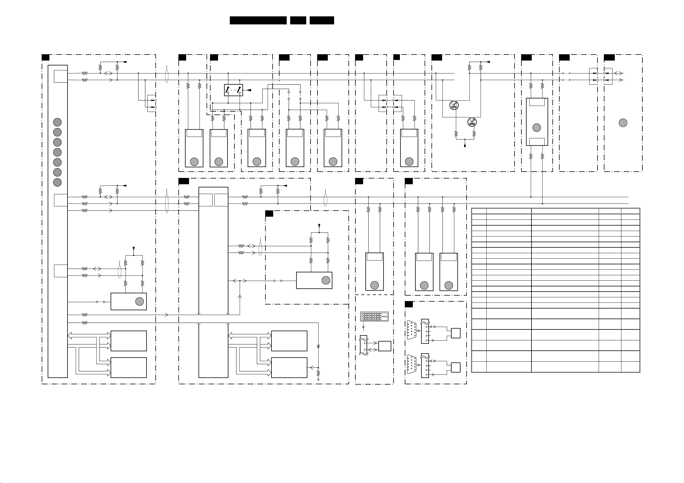
I2C-IC Overview
IIC
CONTROL
SC7
FUNCTIONS 1
86
MASTER
HW IIC
85
7383
SAA5801H
OTC
MAIN-
PROCESSOR
(MASTER)
ERR
91
ERR
92
ERR
93
ERR
94
ERR
95
ERR
96
ERR
97
88
SLAVE
HW IIC
87
91
MASTER
HW IIC
92
74
108
109
Block Diagrams, Testpoint Overviews, and Wiring Diagram
RESET
3404-C
3404-D
3404-A
3404-B
3398-C
3402-B
3402-A
3384
3007
ADDRESS
ADDRESS
DATA
3414 3415
3410 3413
IIC BUS 4
SDA_NVM_1
SCL_NVM_1
4431
7
PW_RESET
PW_FLASH_RESET
MSM51V18165F
DATA
+5V_STBY_SW
SDA-1
SCL-1
+3V3_CNTR_D
SDA-2
SCL-2
PW_START
+3V3_CNTL_D
3432
3433 3431
5
7430
M24C32
(NVM)
EEPROM
7500
RAM
7506
FLASH
0382
10
SERVICE
COMPAIR
CONNECTION
3430
6
ERR
7
9
IIC BUS 1
(slow 100KHz)
IIC BUS 2
(slow 100KHz)
SC8
3541
SC10
3608
3606
CONTROL
FUNCTIONS 2
3540
14
15
SLAVE
HW IIC
7540
PCF8574AT
I/O EXP.
ERR
3
PW164
A4
MASTER
SW
D6
IIC
E2
EXT INT
SC9
7571
3532
9
SLAVE
HW IIC
7530
PCF8591
ADC
ERR
MASTER
7605
PW164
CO-
PROCESSOR
FOR
SCALER
AND
OSD
CLOCK
GENERATOR
4
SW
22FM242 AB 6.
AUDIO
SC14
PROC.
3
1
+5V
4
15
3531
3604
3605
3602
3603
1
SLAVE
HW IIC
FS6377
CLOCK
GENERATOR
IIC BUS 5
PW_RESET
DATA
ADDRESS
ADDRESS
7570
ERR
5
10
B1
C2
IIC
A1
C4
E3
35703571
16
3601 3600
SC9
DATA
SCL_SW
SDA_SW
NVM
PW_SDA_NVM
PW_SCL_NVM
4581
M29W160DT
13
SLAVE
HW IIC
MSP3415G
AUDIO
PROC.
+3V3_PW
7628
CY62126
RAM
7630
FLASH
7812
ERR
7
48104811
38123813
12
2
7580
M24C32
(NVM)
EEPROM
SOURCE
SC13
SELECT
SCL_AUDIO
SDA_AUDIO
28
SLAVE
HW IIC
TEA6422Q
MATRIX
SWITCH
IIC BUS 3
(slow 100KHz)
+3V3_PW
3583
3582 3581
5
ERR
8
6630
3633
7798
ERR
1
PW_SDA
PW_SCL
3580
6
37943795
27
SC8
SC4
0375
6
7
CONTROL
FUNCTIONS2
VIDEO-SEL.
ADC
92
SLAVE
HW IIC
7170
AD9887KS
ADC +
TMDS REC.
ERR
10
DVI-D INPUT SOCKET
SCL
SDA
0319
6
7
32103209
91
7215
ST24FC21
DDC
EPROM
PROTECTION
P3
0319
6
7
PCF8574A
74
SLAVE
HW IIC
7370
I/O EXP.
ERR
6
SC5
VCA
VGA1 IN
15P"D"SHELL
CONNECTOR
11
12
13
14
15
VGA2 IN/OUT
15P"D"SHELL
CONNECTOR
11
12
13
14
15
33703371
73
VIDEO-SEL.
DECODER
3250
P10
SLAVE
HW IIC
7225
SAA7118E
VIDEO
DECODER
ERR
VGA
CONNECTOR
0371
6
1
7
12
2
8
3
13
9
4
10
14
5
15
0372
6
1
7
12
2
8
3
13
9
4
10
14
5
15
9
SC12
3251
N9
DCC-SDA-1
DCC-SCL-1
DCC-SDA-2
DCC-SCL-2
BACK-END
LVDS OUTPUT
SDA-1
SCL-1
7676
BSN20
DS
G
3284
21
SLAVE
HW IIC
7280
SDA9400
DE-
INTERLACER
ERR
11
7904
ST24FC21
5
DDC
7
NVM
7907
ST24FC21
5
DDC
7
NVM
7675
BSN20
DS
G
+3V3_STBY_SW
3285
20
36863682
+3V3_STBY_SW
36853681
SDA-1_3V3
SCL-1_3V3
SC11
EP1K30FC256
BACK-END
EPLD
3664
C5 C4
SLAVE
IIC
7656
EPLD
ERR
12
SLAVE
IIC
C8
C6
3663 3661
3662
SC12
4680
4684
BACK-END
LVDS OUTPUT
0301
16
18
PLASMA DISPLAY
PDP
PANEL
6
7
SDA-1_3V3
SCL-1_3V3
ERR
30
PW_SDA
PW_SCL
Error Device Description Item Diagr.
1
TEA6422D Audio switch (only
2
MSP3451G Sound processor 7812 SC14
3
PCF8574-SCAVIO I/O expander SCAVIO 7540 SC8
4
PCF8591 AD-DA expander 7530 SC8
5
FS6377 Clock generator 7570 SC9
6
PCF8574-PSU I/O expander PSU 7370 P3
7
24C16 OTC NVM OTC 7430 SC7
8
24C16 PW NVM PW 7580 SC9
9
SAA7118 Video decoder
10
AD9887 ADC/TMDS receiver 7170 SC4
11
SDA9400 De-interlacer (only
12
EP1K30QC EPLD processor 7656 SC11
13
PDP I2C error of the PDP
20
Download comm. Errors during downloading
21
CSP comm. CSP time-out error
40
Temperature alarm Detections of over-temperature
70
Over voltage Vs, Va, +5V, +3V3 overvoltage
(only
Enhanced
Enhanced
Enhanced
) 7798 SC13
) 7225 SC5
) 7280 SC5
Black
P
box
71
Vs under voltage Vs under voltage Black
P
box
72
Va under voltage Va under voltage Black
P
box
73
+5V under voltage +5V under voltage Black
P
box
74
+3V3 under voltage +3V3 under voltage Black
P
box
75
DC-PROT Audio amplifier protection Black
P
box
HW = HARDWARE
SW = SOFTWARE
CL 36532011_019.eps
210303
Page 23
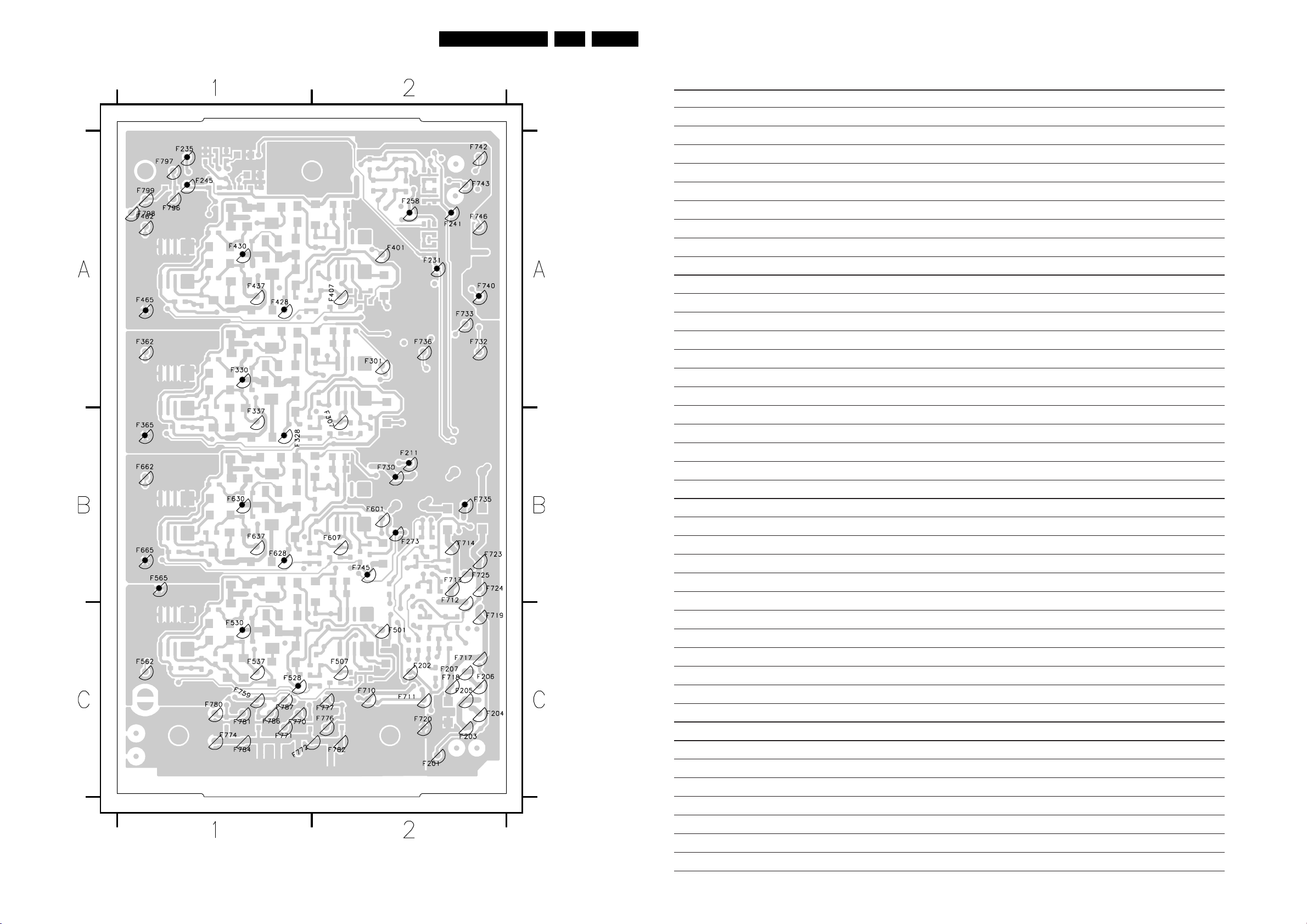
Block Diagrams, Testpoint Overviews, and Wiring Diagram
Testpoint Overview: Audio Amplifier Panel
23FM242 AB 6.
Personal Notes:
CL 26532038_024.eps
150402
F201 C2
F201 C2
F202 C2
F202 C2
F203 C2
F203 C2
F204 C2
F204 C2
F205 C2
F205 C2
F206 C2
F206 C2
F207 C2
F207 C2
F211 B2
F211 B2
F231 A2
F231 A2
F235 A1
F235 A1
F241 A2
F241 A2
F245 A1
F245 A1
F258 A2
F258 A2
F273 B2
F273 B2
F301 A2
F301 A2
F307 B2
F307 B2
F328 B1
F328 B1
F330 A1
F330 A1
F365 B1
F365 B1
F401 A2
F401 A2
F407 A2
F407 A2
F428 A1
F428 A1
F430 A1
F430 A1
F465 A1
F465 A1
F501 C2
F501 C2
F507 C2
F507 C2
F528 C1
F528 C1
F530 C1
F530 C1
F565 B1
F565 B1
F601 B2
F601 B2
F607 B2
F607 B2
F628 B1
F628 B1
F630 B1
F630 B1
F665 B1
F665 B1
F710 C2
F710 C2
F711 C2
F711 C2
F712 B2
F712 B2
F713 B2
F713 B2
F714 B2
F714 B2
F717 C2
F717 C2
F718 C2
F718 C2
F719 C2
F719 C2
F720 C2
F720 C2
F723 B2
F723 B2
F724 B2
F724 B2
F725 B2
F725 B2
F730 B2
F730 B2
F732 A2
F732 A2
F733 A2
F733 A2
F735 B2
F735 B2
F736 A2
F736 A2
F740 A2
F740 A2
F742 A2
F742 A2
F743 A2
F743 A2
F745 B2
F745 B2
F746 A2
F746 A2
F759 C1
F759 C1
F770 C1
F770 C1
F771 C1
F771 C1
F772 C1
F772 C1
F774 C1
F774 C1
F776 C2
F776 C2
F777 C2
F777 C2
F780 C1
F780 C1
F781 C1
F781 C1
F782 C2
F782 C2
F784 C1
F784 C1
F786 C1
F786 C1
F787 C1
F787 C1
F796 A1
F796 A1
F797 A1
F797 A1
F798 A1
F798 A1
F799 A1
F799 A1
Page 24
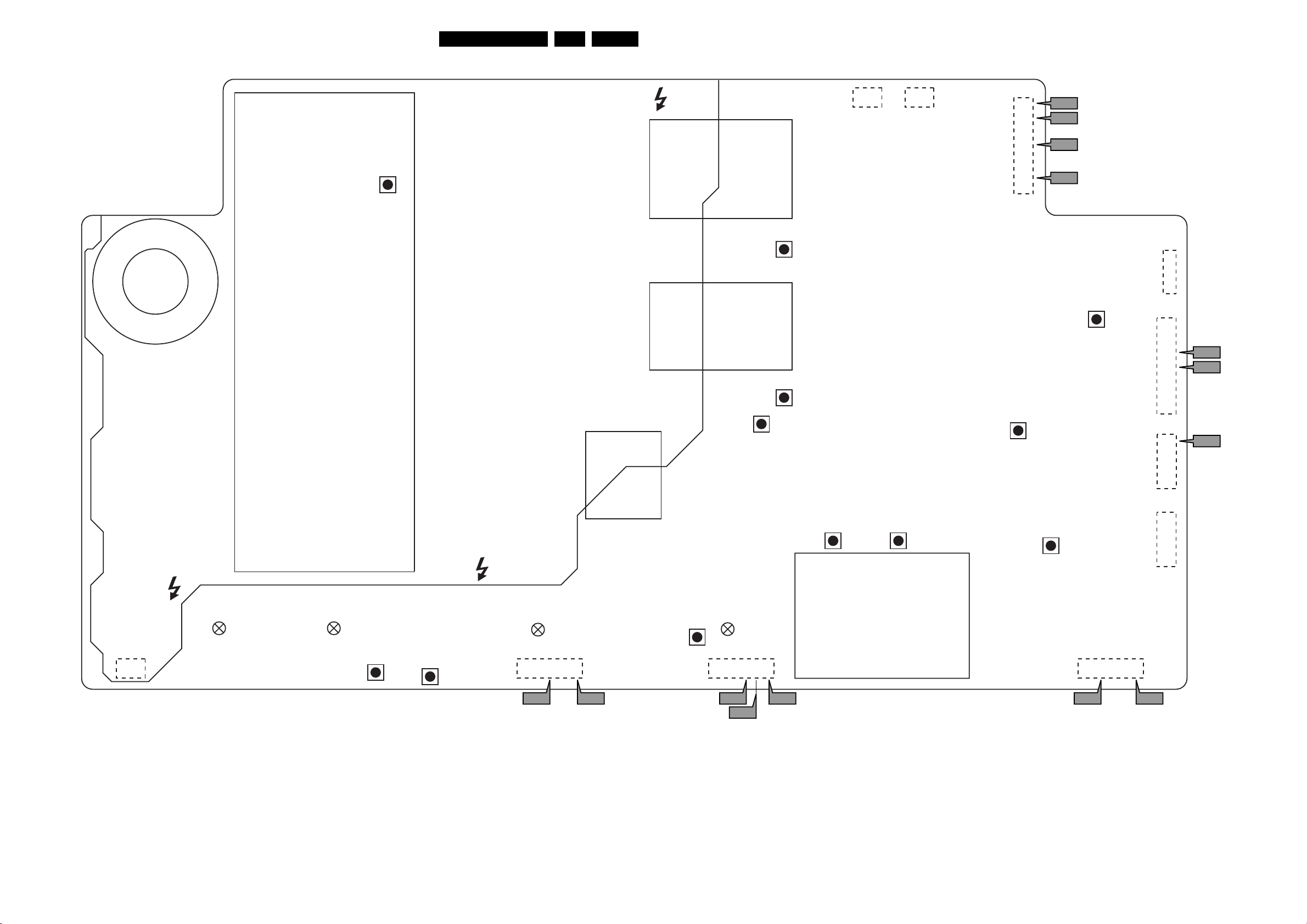
Block Diagrams, Testpoint Overviews, and Wiring Diagram
Testpoint Overview: Power Supply
24FM242 AB 6.
PFC
VR8001
COIL
COIL
8005
13
8007
VSCAN
1
2
5
8
9
P8
P9
P10
P11
VE
VR8005
8003
8008
1
4
5
10
1
9
P12
P13
COLDHOT
VS
VR8008
VA
VR8010
Vcc
13
8006
HOT
8004
COIL
VR8009
8V6 VFAN
VR8007 VR8006
VR8004
VSET
VR8003
HOT
COLD
GREEN
8001
13
COLD
GREEN
8002
5V_STBY_S
VR8002 VR8011
3V3_VSB_S
GREEN
8003
8009
1510
P7 P6 P2 P1
VR8012
DV5
RED
8004
8002
13413
P5 P3
P4
COMPONENT SIDE
Protection
Board
8001
CL 36532011_009.eps
8010
8011
1812
1
5
1
5
200303
P14
Page 25
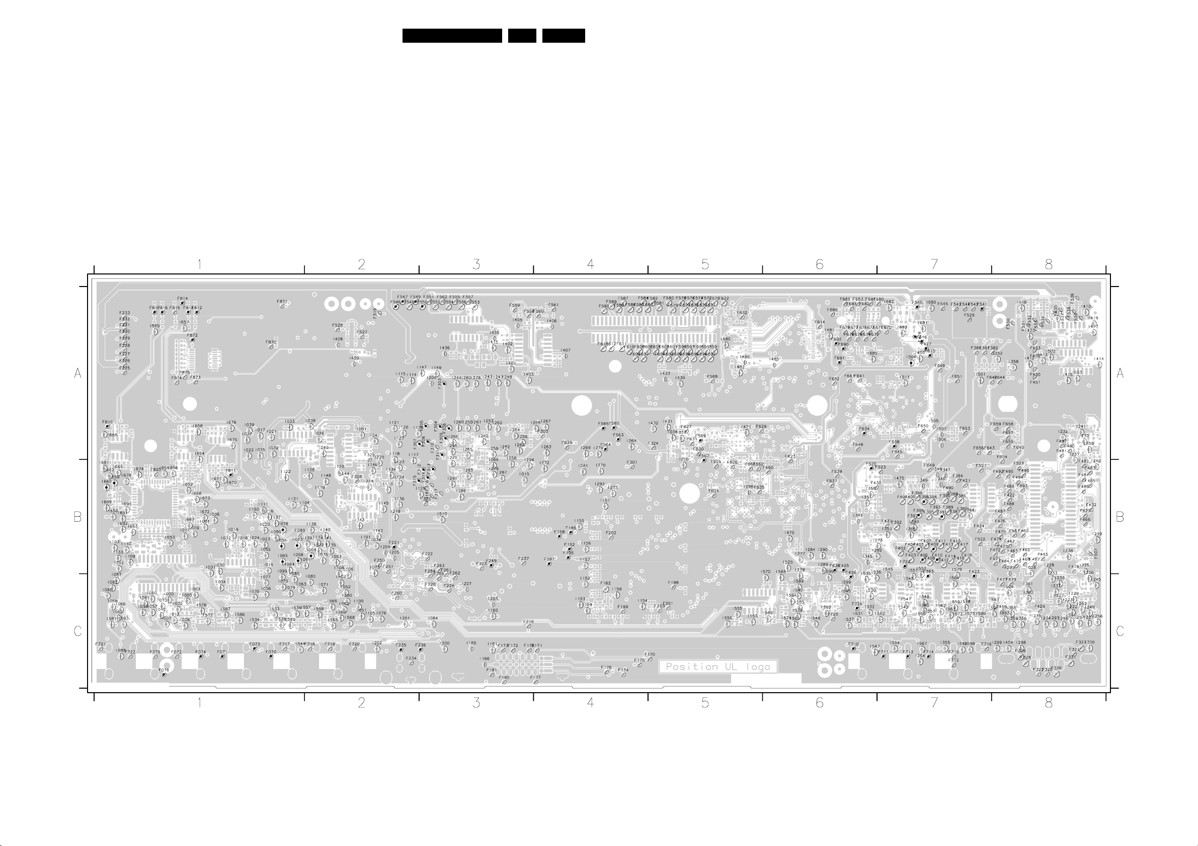
Block Diagrams, Testpoint Overviews, and Wiring Diagram
Testpoint Overview: SCAVIO Panel
F070 C1
F071 C1
F072 C1
F073 C1
F074 C1
F075 C1
F076 C1
F089 B1
F146 B4
F152 B4
F158 B4
F162 C4
F170 C5
F171 C4
F172 C3
F173 C3
F174 C4
F175 C4
F176 C4
F177 C4
F178 C3
F180 C3
F181 C3
F196 B4
F197 B4
F198 C5
F199 C4
F201 C5
F202 B4
F203 C5
F210 C3
F211 C3
F216 C3
F220 C3
F221 B2
F222 B3
F223 B3
F224 C3
F225 A1
F226 A1
F227 A1
F228 A1
F229 A1
F230 A1
F231 A1
F232 A1
F233 A1
F234 C2
F235 C2
F236 C3
F237 B3
F240 B3
F241 B3
F242 B3
F245 B5
F246 B5
F247 B5
F249 B3
F250 B2
F251 B2
F260 C2
F261 C3
F262 C3
F263 B3
F264 C3
F265 C3
F300 A4
F301 B4
F303 A3
F304 A3
F305 A3
F306 A3
F307 A3
F308 A3
F309 A3
F310 A3
F311 A3
F312 B3
F313 B3
F314 B3
F315 B2
F316 B3
F317 B3
F318 B3
F319 A2
F320 C8
F321 C8
F322 C8
F323 B3
F324 A5
F325 A2
F326 B2
F327 C8
F328 C8
F329 C8
F330 C8
F331 C8
F380 A7
F381 A7
F382 A8
F383 C7
F384 B7
F385 B7
F386 B7
F387 B7
F388 B7
F389 B7
F390 B7
F391 B7
F392 B7
F393 B7
F394 B7
F395 B7
F396 B7
F397 B7
F398 B7
F399 B7
F400 B7
F401 B7
F402 B7
F403 B7
F404 B7
F405 B7
F406 B7
F407 B7
F408 B7
F409 B7
F410 B7
F411 B7
F412 B7
F413 B7
F414 B7
F415 B7
F416 B7
F417 B7
F418 B7
F419 B7
F420 B8
F421 B7
F422 B8
F423 C7
F424 B7
F425 B6
F426 C6
F427 A7
F428 A7
F429 C8
F430 B6
F431 B7
F432 B8
F450 A8
F451 A8
F452 A8
F453 A8
F459 C8
F460 B8
F461 B8
F462 B8
F463 B8
F464 B8
F465 B8
F466 B8
F467 B8
F468 B8
F469 B8
F470 B8
F471 B8
F472 B8
F473 B8
F474 B8
F475 B8
F476 B8
F477 C8
F478 B8
F479 C8
F480 A8
F481 A8
F482 B8
F483 B8
F484 B8
F485 B8
F486 B8
F487 B8
F488 B8
F489 B8
F490 B7
F492 B8
F493 B8
F494 B8
F495 B8
F496 B8
F497 A8
F506 B8
F507 B8
F520 B6
F521 B7
F522 B7
F523 B7
F524 B8
F525 B6
F526 B6
F527 A2
F528 A2
F529 A7
F530 A8
F531 A8
F532 A8
F533 A8
F534 A8
F535 A8
F536 A8
F537 A8
F538 A8
F539 A8
F540 A7
F541 A7
F542 A7
F543 A7
F544 A7
F545 A7
F546 A2
F547 A2
F548 A2
F549 A2
F550 A3
F551 A3
F552 A3
F553 A3
F554 A3
F555 A3
F556 A3
F557 A3
F558 A3
F559 A3
F560 A4
F561 A4
F562 A3
F563 A4
F564 A4
F565 A4
F566 A4
F567 B5
F568 A5
F569 A5
F570 A5
F571 A5
F572 A5
F573 A5
F574 A5
F575 A5
F576 A5
F577 A5
F578 A5
F579 A5
F580 A5
F581 A5
F582 A5
F583 A4
F584 A4
F585 A4
F586 A4
F587 A4
F588 A4
F589 A4
F590 A4
F591 A5
F592 A5
F593 A5
F594 A5
F595 A5
F596 A5
F597 A5
F598 A5
F599 A5
F600 A5
F601 A5
F602 A5
F603 A5
F604 A5
F605 A5
F606 A4
F607 A4
F608 A4
F609 A4
F610 A4
F611 A4
F612 A4
F613 A4
F614 A6
F615 A7
F616 A7
F617 A5
F618 B4
F619 B5
F620 B5
F621 B4
F622 A5
F623 B6
F624 B5
F625 B5
F626 B5
F627 A5
F628 A4
F629 A5
F630 A5
F631 A5
F632 A5
F633 B5
F634 A6
F635 B5
F636 B6
F637 B6
F638 A7
F639 B6
F640 A8
F641 A6
F642 A8
F643 A7
F644 A8
F645 A7
F646 A7
F647 A6
F648 A6
F649 B7
F650 A7
F651 A7
F652 A6
F653 A7
F654 B8
F655 A8
F656 A7
F657 A8
F658 A8
F659 A8
F660 B6
F661 B5
F662 B5
F670 A7
F671 A7
F672 A6
F673 A6
F674 A6
F675 A6
F676 A6
F677 A6
F678 A6
F679 A6
F680 A7
F681 A6
F682 A6
F683 A6
F684 A6
F685 A6
F686 A6
F690 A6
F691 A6
F692 A6
F710 C6
F711 C7
F712 C7
F713 C7
F714 C7
F715 C7
F716 C7
F717 C1
F718 C2
F719 C2
F720 C2
F721 C1
F722 C1
F723 B7
F724 C6
F725 C6
F810 A1
F811 B1
F812 A1
F813 A1
F814 A1
25FM242 AB 6.
F815 A1
F816 A1
F817 A1
F820 B1
F870 A1
F871 A1
F872 A1
F873 A1
F874 A1
F875 A1
I001 A2
I0010 C1
I002 C1
I003 C1
I004 B1
I005 C1
I006 B1
I007 C1
I008 C1
I009 B1
I010 C1
I011 B1
I012 C1
I013 C1
I014 B1
I015 B3
I016 B5
I017 A1
I018 B1
I019 B1
I020 B1
I021 A1
I022 A1
I023 B1
I024 B1
I025 A1
I026 A2
I027 A1
I028 B8
I029 A1
I030 B1
I031 B1
I032 B1
I033 A1
I034 C1
I035 C1
I036 A5
I037 A5
I038 A2
I039 A1
I040 A2
I041 A2
I050 C2
I051 C2
I052 C2
I053 B2
I054 B1
I055 B1
I056 C1
I057 C1
I058 B1
I059 C1
I060 C1
I061 B2
I062 C2
I063 C1
I064 B1
I065 B1
I066 C1
I067 C1
I068 C1
I069 B2
I070 C1
I071 C2
I072 B2
I073 B2
I074 B2
I075 B2
I076 C2
I077 C1
I078 B1
I079 C1
I080 C2
I081 C1
I082 C1
I083 B1
I084 C3
I085 C1
I086 C1
I087 C1
I088 C1
I090 B1
I099 C1
I100 C2
I101 B2
I102 B1
I103 B1
I104 B1
I105 C2
I106 C2
I107 C2
I108 B2
I109 B1
I110 B1
I111 B1
I112 B2
I113 B2
I114 A2
I115 A2
I116 B1
I117 B2
I118 B2
I119 B2
I120 A2
I121 A2
I122 B1
I123 B2
I124 B2
I125 B2
I126 A2
I127 A2
I128 B2
I129 B3
I130 B2
I131 B1
I133 B1
I134 B2
I135 B2
I137 B1
I138 B2
I139 B2
I140 B2
I141 B2
I142 B2
I143 B2
I144 B2
I145 B2
I146 B2
I147 A3
I148 B2
I149 A3
I150 B1
I151 B4
I152 C4
I153 C4
I154 C4
I155 B4
I156 B4
I157 B4
I158 C4
I159 C4
I160 C3
I161 C3
I165 C3
I166 C3
I200 C3
I201 C2
I202 C2
I203 C3
I204 A3
I205 B2
I206 B2
I207 C3
I218 B2
I219 B8
I220 B2
I221 C8
I222 C8
I223 C8
I224 B2
I225 B8
I226 C8
I227 C8
I228 B8
I229 C8
I230 A8
I231 B8
I232 A8
I233 C8
I234 C8
I235 C8
I236 C8
I237 C8
I238 B8
I239 A8
I240 B8
I241 A8
I242 A3
I243 A3
I244 A3
I245 C8
I246 C8
I247 A3
I248 A3
I249 C8
I250 A3
I251 A3
I252 C8
I253 A3
I254 A3
I255 A3
I256 C8
I257 C8
I258 B3
I259 A3
I260 A3
I261 A3
I262 A3
I263 A4
I264 A4
I265 A3
I266 B3
I267 A4
I268 A4
I269 A4
I270 B4
I271 B3
I272 B4
I273 B7
I274 A4
I275 B4
I276 B3
I277 B6
I278 A3
I279 C6
I280 A3
I281 B4
I282 A3
I283 A3
I284 B6
I285 B3
I286 B3
I287 B3
I288 A3
I289 B6
I290 B6
I291 B3
I292 B6
I293 B4
I294 B3
I295 B8
I296 B5
I297 C8
I298 C8
I299 C8
I300 C8
I301 C8
I344 B6
I345 B6
I346 B7
I347 B7
I348 B7
I349 B7
I350 B6
I351 B6
I352 A8
I353 B7
I354 C7
I355 C7
I356 C8
I357 C7
I358 A8
I359 C8
I360 C7
I361 C8
I362 C8
I363 B7
I364 B7
I365 C8
I366 B7
I400 A7
I401 A3
I402 A3
I403 A3
I404 C8
I405 A3
I406 A4
I407 A4
I408 A2
I409 A2
I410 A8
I411 A8
I412 A8
I413 A8
I414 A8
I415 A3
I416 A8
I417 A8
I418 A8
I419 A8
I420 A8
I430 A5
I431 A5
I432 A5
I433 A5
I435 A3
I436 A3
I470 B6
I471 A5
I475 B7
I480 A5
I481 A6
I482 A5
I485 A6
I486 A5
I501 A7
I502 A8
I503 A8
I504 A7
I505 A7
I506 A7
I507 A7
I510 B3
I511 A7
I525 B6
I530 C6
I531 C6
I532 C6
I533 C1
I534 C1
I535 C6
I536 C6
I537 C6
I538 C1
I539 C1
I540 C1
I541 C7
I542 C7
I543 C7
I544 C1
I545 C7
I546 C7
I547 C6
I548 C7
I549 C6
I550 C7
I551 C7
I552 C7
I553 C5
I554 C7
I555 C5
I556 C5
I557 C2
I558 C2
I559 C7
I560 C2
I561 C6
I562 C7
I563 C7
I564 C7
I565 C2
I566 C2
I567 C7
I568 C2
I569 C6
I570 C6
I571 C7
I572 C7
I573 C7
I574 C6
I575 C6
I576 C1
I577 C1
I578 C7
I579 C7
I580 C7
I581 C1
I582 C6
I583 C8
I584 C6
I585 C6
I586 C1
I587 C1
I588 C6
I589 C6
I590 C7
I591 C8
I592 C6
I593 C8
I594 C8
I595 C6
I596 C6
I597 C1
I598 C7
I599 C6
I650 B1
I651 B1
I652 B1
I653 B1
I654 B1
I655 B1
I656 B1
I657 A1
I658 A1
I659 B1
I660 B1
I661 B1
I662 B1
I663 B1
I664 B1
I665 A1
I666 A1
I667 B1
I668 B1
I669 B1
I670 B1
I671 B1
I672 B1
I673 B1
I674 B1
I675 A1
I676 A1
I678 B1
I680 A7
I681 A7
I682 A7
I683 A7
I685 A6
I691 B1
I692 B1
3122 123 6001.7
CL 36532051_031.eps
260603
Page 26
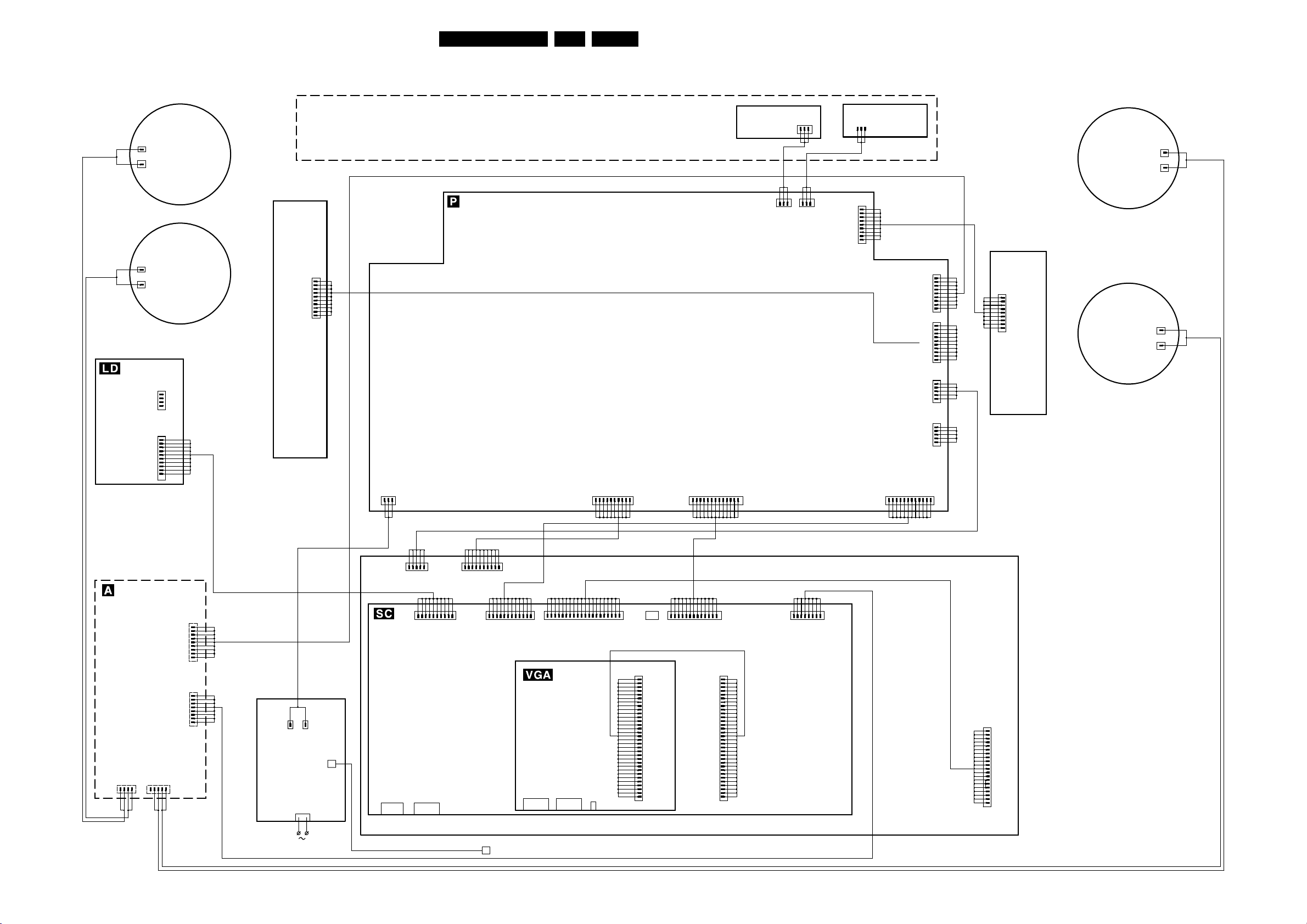
Block Diagrams, Testpoint Overviews, and Wiring Diagram
Wiring Diagram
26FM242 AB 6.
-
+
-
+
LED / SWITCH
PANEL
POS 1072
LIGHT_SENSOR_IN
RC_IN_ICONN
RED_LED
RC_OUT_ICONN
+5V_STBY
GREEN_LED
RED_LED
RC_IN
+8V6
+5V_STBY_SW
+9V_STBY_SW
+9V_STBY
0317
GND
0320
GND
LSP
RIGHT
HIGH
LSP
RIGHT
LOW
1
1
PDP
YM
CN805
FAN
(IF VALID)
1
(IF VALID)
1
FAN
OPTIONAL
LSP
LEFT
HIGH
-
+
1
GND
FAN_SP
1
8005
NC
GND
fAN_SP
8007
Va
1
NC
Vcc
GND
GND
GND
NC
Vs
Vs
Vs
9
PDP
8003
1
VSND_NEG
VSND_NEG
GND_SND
GND_SND
VSND_POS
VSND_POS
GND_SND
9V_STBY
DC_PROT
9
8008
1
D5V
V
G
DND
SCAN
V
GND
V
SET
GND
GND
S
V
V
S
10
8010
1
V
A
V
A
NC
GND
GND
5
8011
1
V
A
V
A
NC
GND
GND
5V
3V3
3V3
3V3
GND
GND
GND
GND
GND
GND
8001
12
N.C.
5
3V3
3V3
1
XM
CN804
LSP
LEFT
LOW
-
+
POWER SUPPLY PANEL
1
10
8006
NC
PDP-SUPPLY
(BLACKBOX)
_ON
8004
AC LINE
3
NC
AC NEUTRAL
1
S
D5V
D3.3V1
GND
GND
D3.3V1
V
GND
RSV
GND
PDP_GO
8009
10
1
8002
13
+9V_STBY
+9V_STBY_SW
+3V3_STBY_SW
+5V_STBY_SW
8V6
SCL-1
SDA-1
GND
STANDBY
POWER_OK
FAN_SP_1
RES
FAN_SP_2
1
AUDIO AMPLIFIER
PANEL (IF VALID)
POS 1050
VSND_NEG
VSND_NEG
VSND_POS
VSND_POS
+9V_STBY
DC_PROT
AUDIO_RIGHT_NEG
AUDIO_RIGHT_POS
RIGHT_GND
AUDIO_ENABLE
LEFT_GND
AUDIO_LEFT_NEG
AUDIO_LEFT_POS
LOW_RIGHT_POS
HIGH_RIGHT_POS
LOW_RIGHT_NEG
HIGH_RIGHT_NEG
0304
1
HIGH_LEFT_POS
N.C.
0303
LOW_LEFT_POS
LOW_LEFT_NEG
HIGH_LEFT_NEG
5
PDP E-BUFFER / F-BUFFER / G-BUFFER / LOGIC BOARD
1
CN806
10
9 pole
D-shell
0320
RED_LED
+5V_STBY
GREEN_LED
4x CINCH
RC_IN
0302
1
GND
GND
GND
0388
1
GND
1
0308
BLUE
MAINS_NEUTRAL
MAINS-inlet
+ Filter
POS 1061
BROWN
MAINS_LIVE
M91
SCAVIO
PANEL
POS 1063
1
GND
+8V6
+9V_STBY
+9V_STBY_SW
+5V_STBY_SW
LIGHT_SENSOR_IN
10
D3.3V1
D3.3V1
1
CN803
D5V
_ON
RSV
GND
GND
GND
GND
S
V
PDP_GO
1
12
0305
5V
GND
GND
1
0301
3V3
3V3
3V3
3V3
3V3
GND
GND
GND
GND
RXIN0-
RXIN0+
GND_LVDS
SCL0
RXIN1-
GND
RXIN1+
SDA0
RXIN2-
RXIN2+
CPU-GO
GND_LVDS
VGA CONNECTOR
PANEL
POS 1032
15 pole
D-shell
1x CINCH
CP91
15 pole
D-shell
PDP-GO
RXCLKIN-
RXCLKIN+
20
IRQ
PDWN
RXIN3-
RXIN3+
GND_LVDS
0318
1
0315
foil
N.C.
+5V_STBY_SW
VGA2_OUTN
RC_OUT
GND
VGA2_RXD
VGA2_TXD
GND
VGA2_V
GND
VGA2_H
GND
VGA2_B
GND
VGA2_G
GND
VGA2_R
GND
RC_VGA1
GND
VGA1_RXD
VGA1_TXD
GND
VGA1_V
GND
VGA1_H
GND
VGA1_B
GND
VGA1_G
GND
VGA1_R
GND
1
0319
+9V_STBY
8V6
SCL-1
+9V_STBY_SW
+5V_STBY_SW
+3V3_STBY_SW
+5V_STBY_SW
RES
GND
SDA-1
POWER_OK
VGA2_OUTN
RC_OUT
VGA2_RXD
VGA2_TXD
VGA2_V
VGA2_H
VGA2_B
VGA2_G
VGA2_R
RC_VGA1
VGA1_RXD
VGA1_TXD
VGA1_V
VGA1_H
VGA1_B
VGA1_G
VGA1_R
STANDBY
FAN_SP_1
1
GND
GND
GND
GND
GND
GND
GND
GND
GND
GND
GND
GND
GND
GND
FAN_SP_2
0318
foil
1
0388
RIGHT_GND
AUDIO_ENABLE
AUDIO_RIGHT_POS
AUDIO_RIGHT_NEG
GND
LEFT_GND
AUDIO_LEFT_POS
AUDIO_LEFT_NEG
CN1
1
20
CL 36532011_001.eps
200303
Page 27
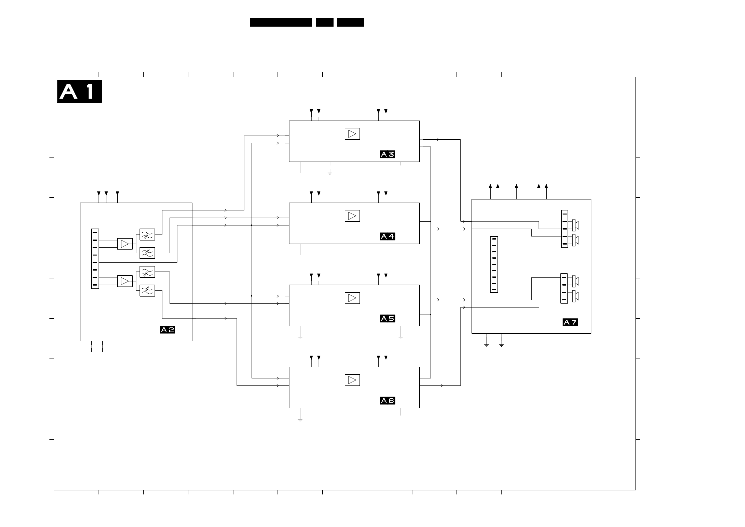
Electrical Diagrams and PWB Layouts
7. Electrical Diagrams and PWB Layouts
Audio Panel & Supply: DC Protection
27FM242 AB 7.
A
B
C
D
E
G
654321
7
1098
131211
AUDIO PANEL
& SUPPLY , DC PROTECTION
L_HIGH
AU_EN_NOT
VCC_10_POS
VCC_10_NEG
+9V_STBYA
L_HIGH
L_HIGH
L_LOW
R_HIGH
R_LOW
L_LOW
AU_EN_NOT
R_HIGH
R_LOW
+9V_STBYA
VCC_10_POS
8
1
0388
PH-S
VCC_10_NEG
GND_F
L_POS
L_NEG
GND_F
AUDIO_ENABLE
GND_F
R_POS
R_NEG
AU_EN_NOT
F
L_LOW
AU_EN_NOT
AU_EN_NOT
R_HIGH
FILTERS
L_HIGH
AU_EN_NOT
GND_I
GND_I
L_LOW
AU_EN_NOT
GND_I
AU_EN_NOT
R_HIGH
GND_I
GND_I
VCC_10_POS
VCC_10_NEG
VCC_10_POS
VCC_10_NEG
VCC_10_POS
VCC_10_POS
VCC_10_NEG
VCC_10_POS
VCC_10_NEG VCC_10_NEG
VCC_10_POS
VCC_10_NEG
AMPLIFIER LEFT_HIGH
DIAGRAM
GND
AMPLIFIER LEFT_LOW
DIAGRAM
AMPLIFIER RIGHT_HIGH
DIAGRAM
DIAGRAM
GND
GND_F
GND_F
GND_I
VCC_10_POS
VCC_10_NEG
VSND_POS
VSND_NEG
VSND_POS
VSND_NEG
VSND_POS
VSND_NEG
VSND_POS
VSND_NEG
VSND_POS
VSND_NEG
VSND_POS
VSND_NEG
VSND_POS
VSND_NEG
GND_O
GND_O
GND_O
GND_O
GND_O
GND_O
OUT_LH
OUT_PROT
OUT_PROT
OUT_LL
OUT_RH
OUT_PROT
OUT_LH
OUT_LL
OUT_RH
OUT_PROT
OUT_LH
OUT_LL
OUT_RH
OUT_RL
OUT_PROT
GND GND_O
VCC_10_POS
VCC_10_POS
0302
9
1
PH-S
VCC_10_NEG
VCC_10_NEG
DC_PROT
+9V_STBY
GND
VSND_POS
VSND_POS
GND
GND
VSND_NEG
VSND_NEG
+9V_STBYA
+9V_STBYA
VSND_POS
VSND_POS
OUT_RH
OUT_RL
SUPPLY & DC PROTECTION
DIAGRAM
GND_O
VSND_NEG
VSND_NEG
GND_O
OUT_LH
OUT_LL
GND_O
GND_O
GND_O
5
1
4
1
0303
PH-S
0304
PH-S
A
B
C
D
E
F
G
H
AU_EN_NOT
R_LOW
AU_EN_NOT
VCC_10_POS
VCC_10_NEG
VSND_POS
VSND_NEG
OUT_PROT
OUT_RLR_LOW
OUT_RL
H
AMPLIFIER RIGHT_LOW
GND_I
I
GND_I
J
1
432 131211
5
6
DIAGRAM
7
GND_O
GND_O
I
J
CL 26532038_015.eps
290302
1098
Page 28
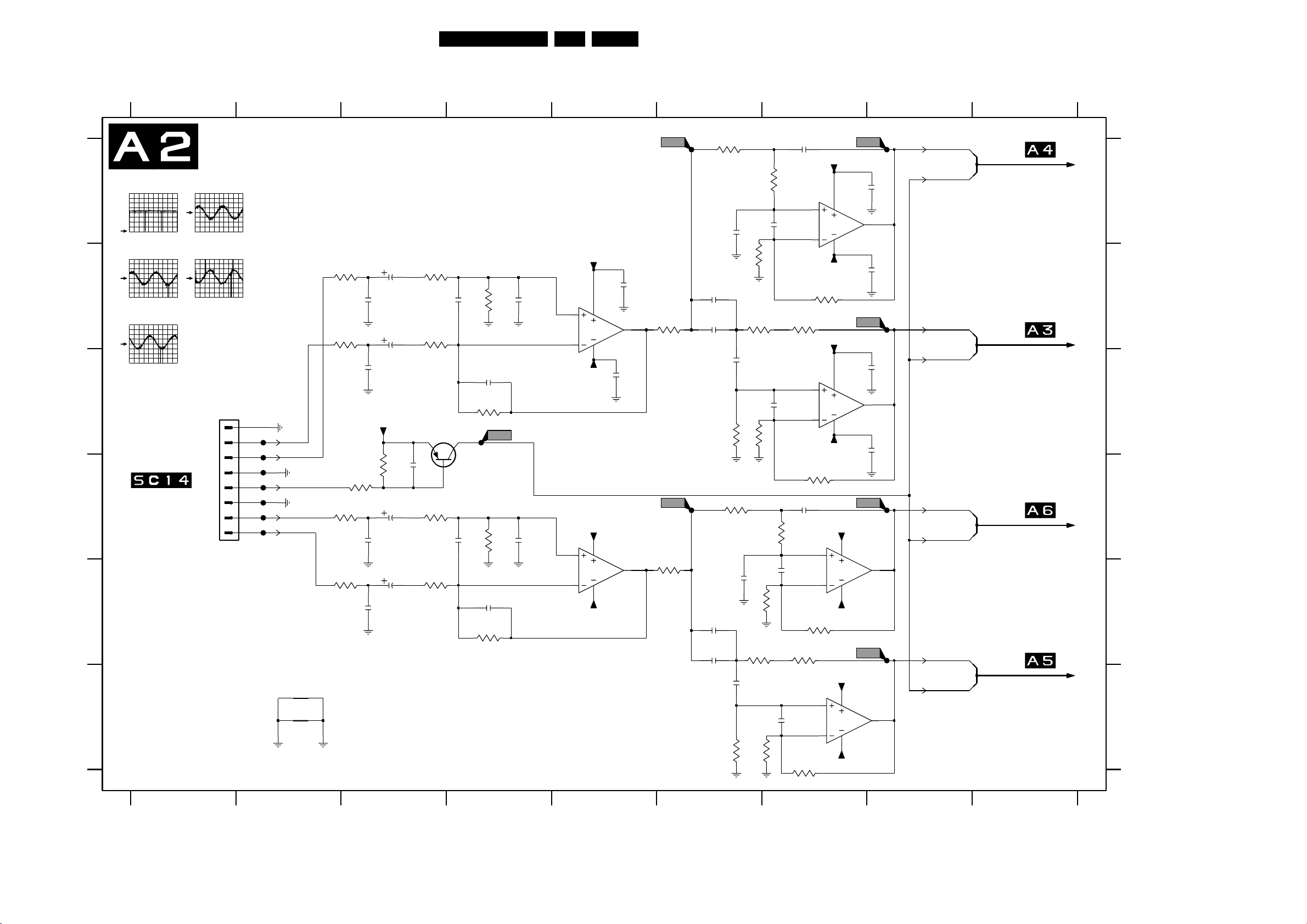
Electrical Diagrams and PWB Layouts
Audio Panel & Supply: Filters
28FM242 AB 7.
A
B
F211
1V / div DC
5ms / div
F231
50mV / div DC
200µs / div
F235
50mV / div DC
200µs / div
C
FROM 0388
D
SCAVIO PANEL
(AUDIO-PROCESSOR)
E
F
1
F241
50mV / div DC
F245
50mV / div DC
F258 = 0V
F278 = 0V
FILTERS
200µs / div
200µs / div
0388
PH-S
8
F201
7
F202
6
F203
5
F204
4
F205
3
F206
2
F207
1
GND_F
2
GND_F
L_POS
L_NEG
GND_F
AUDIO_ENABLE
GND_F
R_POS
R_NEG
C203
C202
3201
220R
GND_F
3205
220R
GND_F
3215
220R
GND_F
3220
220R
2201
2205
3210
33K
2215
2220
GND_F
3
2202
10u
4n7
2206
10u
4n7
+9V_STBYA
3211
100K
2216
10u
4n7
2221
10u
4n7
2212
3202
1K
3206
1K
7211
BC857BW
1n
8V7
3216
1K
3221
1K
2203
0V
2217
RES
RES
3203
GND_F
2207
82p
3207
2K7
F211
3217
GND_F
2222
82p
3222
2K7
4
2K7
2K7
2204
GND_F
2218
GND_F
82p
82p
VCC_10_POS
7225-A
LM833DT
3
0V
2
0V
VCC_10_NEG
GND_F
VCC_10_POS
5
0V
6
0V
VCC_10_NEG
5
8
4
8
4
2225
GND_F
0V
1
2224
100n
7225-B
LM833DT
7
F231
100n
3230
100R
F241
3240
100R
6
2254
RES
2255
22n
GND_F
GND_F
2269
RES
2270
22n
GND_F
3231
2K2
2233
GND_F
2256
3256
3241
2K2
2271
3271
2243
68n
3233
GND_F
3255
1K2
22n
3K3
3258
GND_F
68n
3243
GND_F
3270
1K2
22n
3K3
3273
GND_F
3232
2232
2K2
2257
RES
3242
2242
2K2
2272
RES
2234
100n
1K5
RES
3257
470R
RES
2244
100n
1K5
RES
3272
470R
RES
3274
7
VCC_10_POS
7238-A
LM833DT
3
0V
2
0V
VCC_10_NEG
3234
560R
VCC_10_POS
7260-A
LM833DT
3
0V
2
0V
VCC_10_NEG
3259
1R
VCC_10_POS
5
0V
6
0V
VCC_10_NEG
3244
560R
VCC_10_POS
5
0V
6
0V
VCC_10_NEG
1R
8
4
GND_F
8
4
GND_F
8
4
8
4
F235
2238
GND_F
0V
1
2239
F258
2260
GND_F
1
2261
F245
7238-B
LM833DT
7
0V
F273
7260-B
LM833DT
7
0V
100n
100n
100n
0V
100n
1234567
89
L_LOW
AU_EN_NOT
TO DIAGRAM
AMPLIFIER
LEFT_LOW
A
B
L_HIGH
AU_EN_NOT
TO DIAGRAM
AMPLIFIER
LEFT_HIGH
C
R_LOW
AU_EN_NOT
TO DIAGRAM
D
AMPLIFIER
RIGHT_LOW
E
R_HIGH
AU_EN_NOT
TO DIAGRAM
AMPLIFIER
RIGHT_HIGH
F
CL 26532038_016.eps
030502
89
0388 C1
2201 B3
2202 B3
2203 B4
2204 B4
2205 C3
2206 B3
2207 C4
2212 D3
2215 D3
2216 D3
2217 D4
2218 D4
2220 E3
2221 E3
2222 E4
2224 C5
2225 B5
2232 A7
2233 A6
2234 A7
2238 A7
2239 B7
2242 E7
2243 E6
2244 D7
2254 B6
2255 B6
2256 C6
2257 C7
2260 C7
2261 C7
2269 E6
2270 E6
2271 F6
2272 F7
3201 B3
3202 B3
3203 B4
3205 B3
3206 B3
3207 C4
3210 D3
3211 D3
3215 D3
3216 D3
3217 D4
3220 E3
3221 E3
3222 E4
3230 B6
3231 A6
3232 A7
3233 B6
3234 B7
3240 E6
3241 D6
3242 D7
3243 E6
3244 E7
3255 B6
3256 C6
3257 B7
3258 C6
3259 D7
3270 E6
3271 F6
3272 E7
3273 F6
3274 F7
7211 C4
7225-A B5
7225-B D5
7238-A A7
7238-B D7
7260-A C7
7260-B F7
C202 F2
C203 F2
F201 C2
F202 C2
F203 D2
F204 D2
F205 D2
F206 D2
F207 D2
F211 C4
F231 A6
F235 A8
F241 D6
F245 D8
F258 B8
F273 E8
Page 29
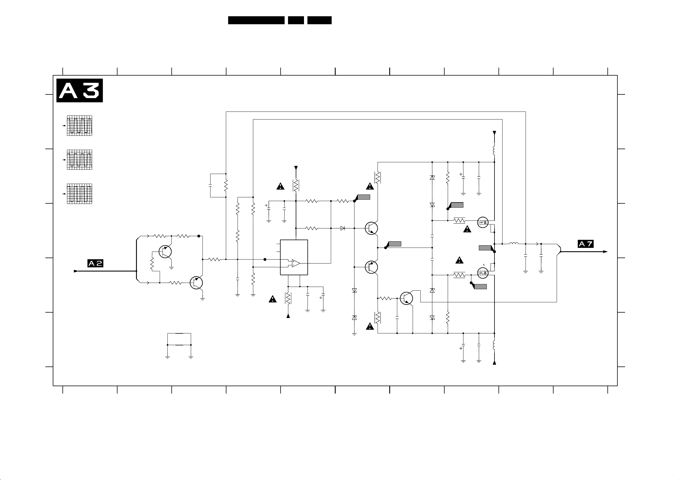
Electrical Diagrams and PWB Layouts
Audio Panel & Supply: Left High
2309 D4 2330 C7
2315 C4
2316 C5
2318 D5
2319 D5
2334 B8
2335 B8
2340 E7
2355 D7
2359 E8 6334 B7
12345678910
AUDIO AMPLIFIER
LEFT HIGH
F328
2360 E8
2365 C9
2366 C9
3301 C3
3302 D32310 B3
3303 C2
3304 D2
3306 C3
3307 C4
29FM242 AB 7.
3308 C4 7340 D7
3309 D4
3310 B3
3311 C4
3315 B5
3318 D5
3325 B5
3327 C5
3328 B6
3330 B6
3336 B8
3337 C8
3340 D6
3355 E6
3361 E8
3362 D8
5335 B8
5360 E8
5365 C9
6328 C6
6335 C7
6355 D6
6356 E6
6359 E7
6360 D7
7302 D3
7303 C3
7315 C4
7330 C6
7355 D6
7365-1 D8
7365-2 C8
C302 E3
F301 C3
F307 C4
F328 B6
F330 C7
F337 C8C301 E3
F362 D8
F365 C8
A
B
C
D
E
2V / div DC
1µs / div
F330
2V / div DC
1µs / div
F365
5V / div DC
1µs / div
FROM DIAGRAM
FILTERS
L_HIGH
3304
AU_EN_NOT
3303
1K
4K7
7303
BC847BW
GND_I
3302
4K7
3301
C302
C301
1K
GND_I
F301
GND_I
82p
2310
3306
8K2
7302
BC847BW
3310
82K
GND_I
3307
3311
2309
100K
1R
1n5
3308
3309
GND_I
100K
F307
180R
2315
GND_I
0V
VCC_10_POS
3315
1u
100n
2316
GND_I
7315
LM311D
5
V+
BAL
6
STR|BAL
2
3
0V
GND
1
-9V8
3318
VCC_10_NEG
9V7
8
V-
10R
10R
4
GND_I
3325
2K2
3327
2K2
7
-2V
2318
100n
2319
GND_I
1u
3328
1K
6328
BAS316
F328
-0V04
6355
6356
GND_I
3330
14V2
7330
BC817-25
-0V04
BC807-25
-14V2
BZX384-C4V7
3355
BZX384-C4V7
10R
7355
3340
10K
10R
F330
-14V2
7340
BC847BW
10n
2340
0V
6334
6335
2330
2355
6360
6359
100n
100n
4M7
3336
2334
BZX384-C4V7
GND_O
F337
3337
BZX384-C4V7
10R
3362
10R
BZX384-C4V7
4M7
3361
BZX384-C4V7
2360
GND_O
-14V4
VSND_POS
220u
2335
GND_O
7365-2
IRF7343
4
7365-1
IRF7343
2
F362
2359
220u
GND_O
100n
14V3
F365
100n
VSND_NEG
5335
3
5
78
1
5360
100MHZ
6
0V
-14V4
100MHZ
5365
33u
2365
GND_O
220n
2366
GND_O
OUT_LH
220n
TO DIAGRAM
SUPPLY & DC
PROTECTION
OUT_PROT
CL 26532038_017.eps
A
B
C
D
E
030502
123
456 10
789
Page 30
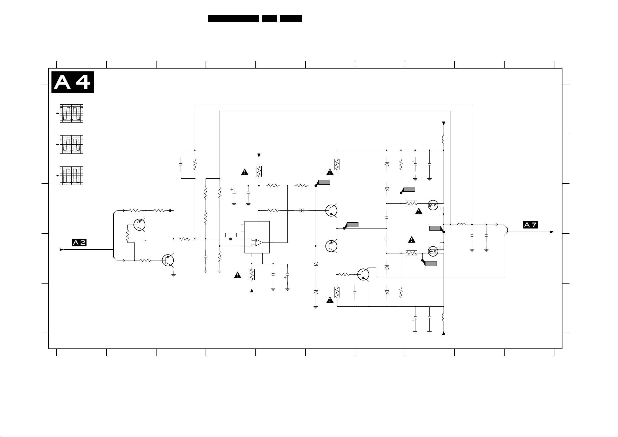
Electrical Diagrams and PWB Layouts
Audio Panel & Supply: Left Low
2409 D3
2410 B3
2415 C4
2416 C4
2418 D5 3402 D2
2419 D5
2430 C7
2434 B8
2435 B8
2440 E6
2455 D7
2459 E8
2460 E8
2465 D9
3401 C3
3403 C2
3404 D2
3406 C3
3407 C3
3408 C4
3409 D4
3410 B3
3411 C3
3415 B4
3418 D4
3425 B5
3427 C5
3428 B5
30FM242 AB 7.
3430 B6
3436 B7
3437 C8
3440 D6
3455 E6
3461 E7
3462 D8
5435 B8
5460 E8
5465 C9
6428 C5
6434 B7
6435 C7
6455 D6
6456 E6
6459 E7
6460 D7
7402 D32466 D9
7403 C2
7415 C4
7430 C6
7440 D7
7455 D6
7465-1 D8
7465-2 C8
F401 C3
F407 D4
F428 B6
F430 C6
F437 C8
F462 D8
F465 C8
A
B
C
D
1234567
AUDIO AMPLIFIER
LEFT LOW
F428
2V / div DC
1µs / div
F430
2V / div DC
1µs / div
F465
5V / div DC
1µs / div
FROM DIAGRAM
FILTERS
L_LOW
3404
AU_EN_NOT
3403
1K
4K7
GND_I
3402
4K7
3401
1K
7403
BC847BW
F401
GND_I
82p
2410
3406
8K2
7402
BC847BW
3410
82K
GND_I
3407
3411
2409
100K
15K
1n5
3408
3409
GND_I
100K
F407
180R
2415
GND_I
0V
1u
5
6
2
3
0V
-9V8
VCC_10_POS
3415
100n
2416
GND_I
9V7
7415
8
LM311D
V+
BAL
STR|BAL
GND
V-
1
10R
3418
4
10R
3425
2K2
3427
2K2
7
-2V
2418
100n
2419
3428
1K
6428
BAS316
1u
F428
-0V04
6455
BZX384-C4V7
3430
10R
14V2
7430
BC817-25
F430
-0V04
7455
BC807-25
-14V2
3440
10K
-14V2
7440
BC847BW
0V
6434
BZX384-C4V7
6435
BZX384-C4V7
100n
2430
100n
2455
BZX384-C4V7
3436
4M7
F437
3437
10R
3462
10R
2434
GND_O
-14V4
89
VSND_POS
5435
100MHZ
220u
100n
2435
GND_O
7465-2
IRF7343
14V3
F465
7465-1
F462
3
56
78
1
0V
-14V4
5465
33u
2465
GND_O
220n
2466
GND_O
OUT_LL
220n
OUT_PROT
4
IRF7343
2
10
A
B
C
TO DIAGRAM
SUPPLY & DC
PROTECTION
D
E
GND_I
VCC_10_NEG
1
345678
GND_I
6456
BZX384-C4V7
GND_I
3455
10R
2440
10n
6459 6460
BZX384-C4V7
3461
4M7
2460
GND_O
220u
2459
GND_O
100n
5460
VSND_NEG
100MHZ
E
CL 26532038_018.eps
030502
9102
Page 31
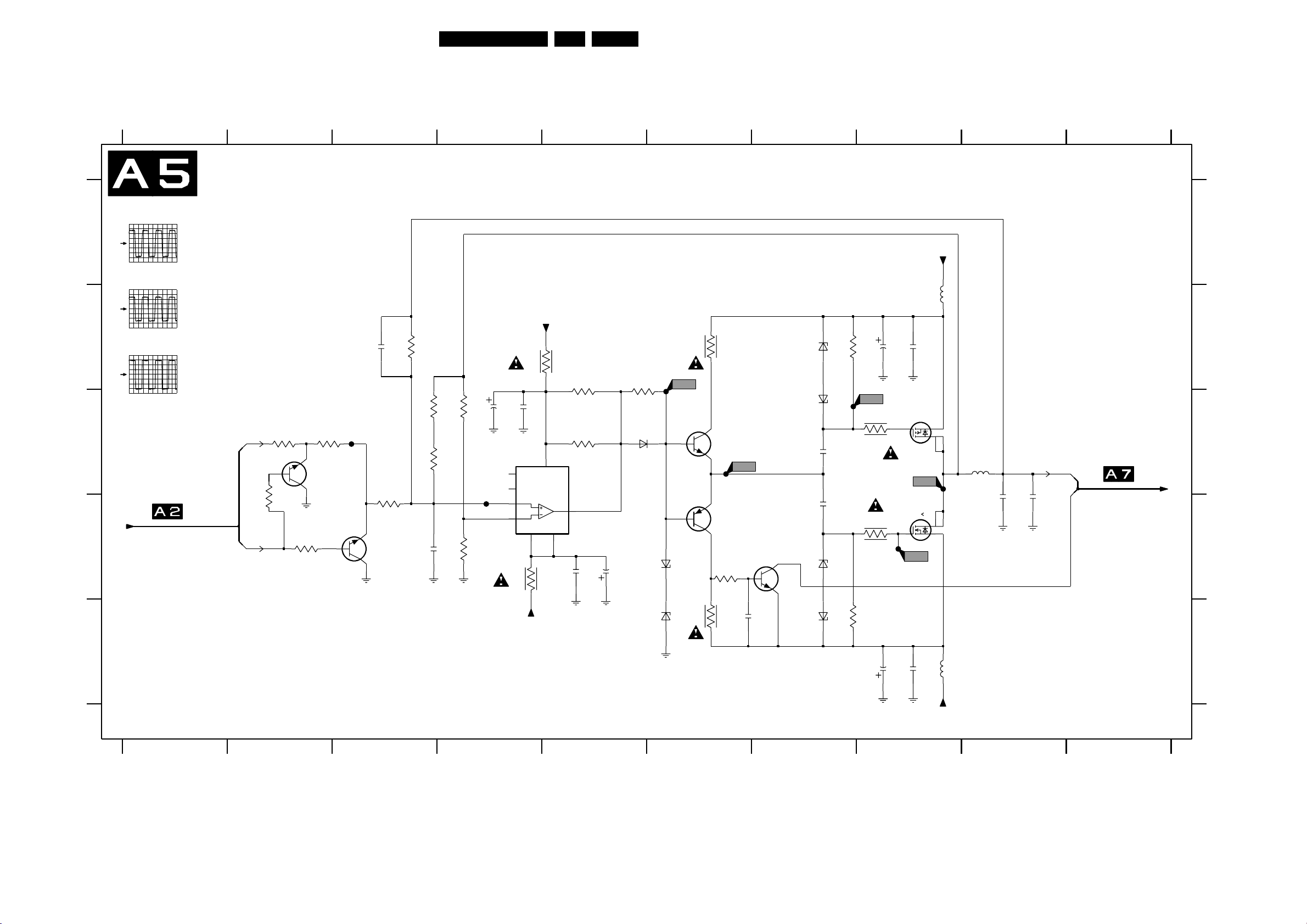
Electrical Diagrams and PWB Layouts
Audio Panel & Supply: Right High
2510 B3
2515 C4
2516 C4
2518 D5
2519 D5
2534 B8
2535 B8
2540 E6
2555 D7
2559 E8
2560 E8
2565 D9
2566 D9
3501 C2
3502 D2
3503 C2
3504 D2
3506 D3
3507 C3
3508 C4
3509 D4
3510 B3
3511 C3
3515 B4
3518 D4
3525 B52509 D3
3528 B5
31FM242 AB 7.
3530 B6
3536 B7
3537 C8
3540 D6
3561 E7
3562 D8
5535 B8
5560 E8
5565 C9
6528 C5
6534 B7
6535 C72530 C7
6555 D6
6556 E6
6559 E7
6560 D7
7502 D3
7503 C2
7515 C4
7530 C6
7540 D7
7555 D6
7565-1 D8
7565-2 C8
F501 C3
F507 D4
F528 B6
F530 C6
F537 C8
F562 D8
F565 C83527 C5 3555 E6
A
B
C
D
E
1234
AUDIO AMPLIFIER
RIGHT HIGH
F528
2V / div DC
1µs / div
F530
2V / div DC
1µs / div
F565
5V / div DC
1µs / div
FROM DIAGRAM
FILTERS
R_HIGH
3504
AU_EN_NOT
3503
1K
4K7
7503
BC847BW
GND_I
3502
4K7
3501
1K
F501
GND_I
82p
2510
3506
8K2
7502
BC847BW
3510
82K
GND_I
3507
3511
2509
100K
6K8
1n5
3508
3509
GND_I
100K
F507
180R
2515
GND_I
0V
VCC_10_POS
3515
1u
2516
100n
GND_I
7515
LM311D
5
V+
BAL
6
STR|BAL
2
3
0V
GND
1
-9V8
3518
VCC_10_NEG
9V7
8
V-
10R
4
10R
3525
2K2
3527
2K2
7
-2V
2518
GND_I
5
100n
2519
GND_I
1u
3528
1K
6528
BAS316
F528
-0V04
6555
6556
GND_I
678 10
VSND_POS
5535
100MHZ
3530
14V2
7530
BC817-25
-0V04
BC807-25
-14V2
BZX384-C4V7
3555
BZX384-C4V7
10R
7555
3540
10K
-14V2
10R
F530
2540
7540
BC847BW
0V
10n
6534
6535
2530
2555
6560
6559
4M7
3536
2534
BZX384-C4V7
GND_O
F537
3537
BZX384-C4V7
10R
100n
100n
3562
10R
BZX384-C4V7
4M7
3561
BZX384-C4V7
2560
-14V4
220u
GND_O
7565-2
IRF7343
4
7565-1
IRF7343
2
220u
2535
F562
2559
100n
14V3
F565
100n
3
6
5
78
1
5560
5565
33u
0V
-14V4
100MHZ
2565
GND_O
9
220n
2566
GND_O
TO DIAGRAM
OUT_RH
220n
SUPPLY & DC
OUT_PROT
PROTECTION
A
B
C
D
E
GND_O
GND_O
VSND_NEG
CL 26532038_019.eps
030502
12345678910
Page 32
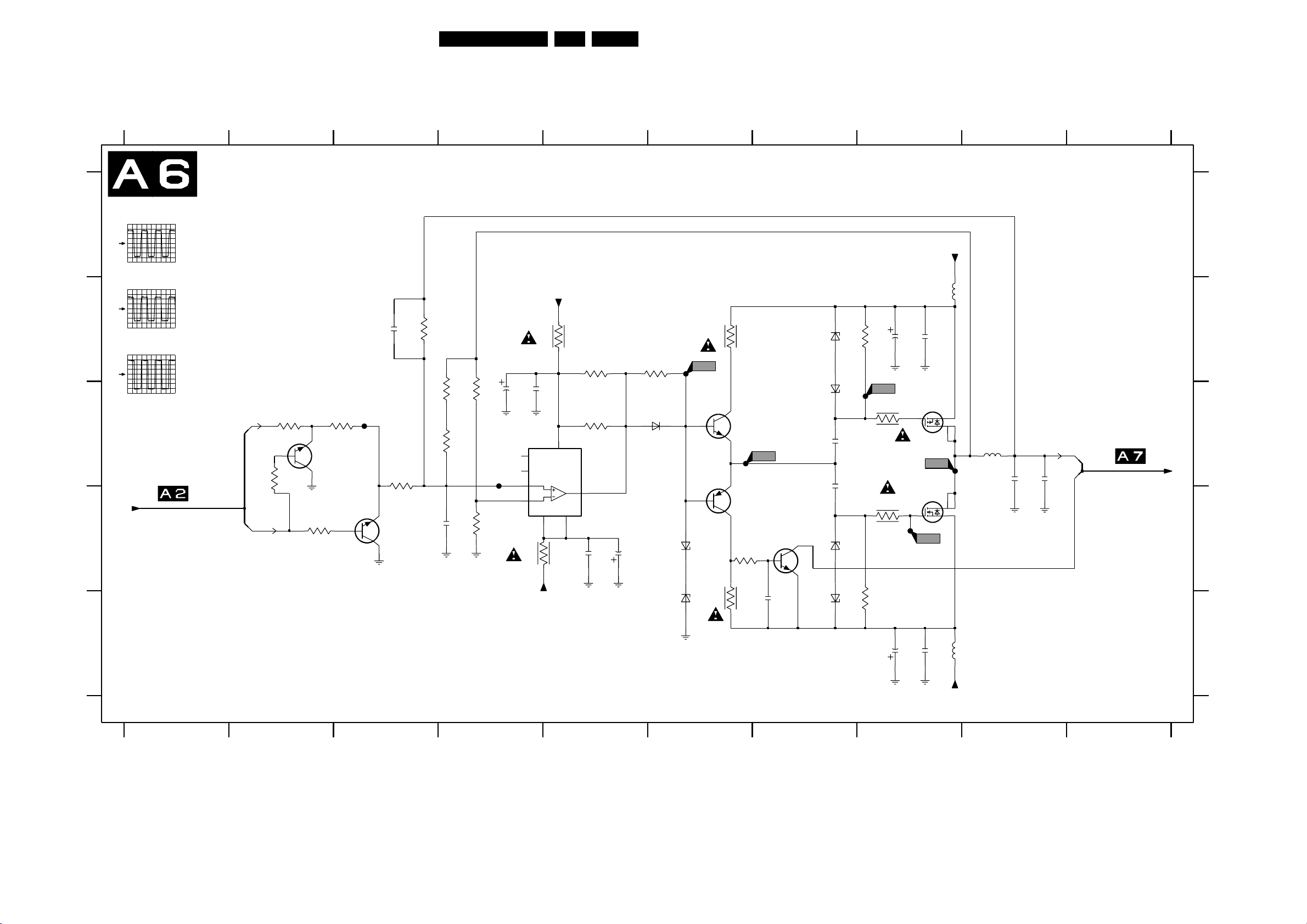
Electrical Diagrams and PWB Layouts
Audio Panel & Supply: Right Low
2609 D4
2610 B3
2615 C4
2616 C4
2618 D5
2619 D5 F637 C8
2630 C7
2634 B8
2635 B8
2640 E7
2655 C7
2659 E8
12345678910
AUDIO AMPLIFIER
RIGHT LOW
32FM242 AB 7.
2660 E8
2665 C9 F665 C8
2666 C9
3601 C3
3602 D2
3603 C2
3604 C2
3606 C3
3607 C4
3608 C4
3609 D4
3610 B3
3611 C4
3615 B5
3618 D4
3625 B5
3627 C5
3628 B6
3630 B6
3636 B8
3637 C8
3640 D6
3655 E6 7655 D6
3661 E8
3662 D8
5635 B8
5660 E8
5665 C9
6628 C6
6634 B7
6635 C7
6655 D6
6656 E6
6659 E7
6660 D7
7602 D3
7603 C2
7615 C4
7630 C6
7640 D7
7665-1 D8
7665-2 C8
F601 C3
F607 C4
F628 B6
F630 C7
F662 D8
A
B
C
D
F628
2V / div DC
1µs / div
F630
2V / div DC
1µs / div
F665
5V / div DC
1µs / div
FROM DIAGRAM
FILTERS
R_LOW
3604
AU_EN_NOT
3603
1K
4K7
7603
BC847BW
GND_I
3602
4K7
3601
1K
F601
GND_I
82p
2610
3606
8K2
7602
BC847BW
3610
82K
3607
3611
2609
100K
22K
1n5
3608
3609
GND_IGND_I
100K
F607
180R
2615
GND_I
0V
VCC_10_POS
3615
1u
2616
100n
GND_I
7615
LM311D
5
V+
BAL
6
STR|BAL
2
3
0V
GND
1
-9V8
3618
VCC_10_NEG
9V7
8
V-
10R
4
10R
3625
2K2
3627
2K2
7
-2V
2618
GND_I
100n
2619
GND_I
1u
3628
1K
6628
BAS316
F628
-0V04
6655
BZX384-C4V7
6656
BZX384-C4V7
3630
7630
BC817-25
-0V04
BC807-25
-14V2
3655
10R
14V2
7655
3640
10K
-14V2
10R
F630
2640
7640
BC847BW
10n
0V
6634
BZX384-C4V7
6635
BZX384-C4V7
2630
100n
100n
2655
6660
BZX384-C4V7
6659
BZX384-C4V7
3636
3661
4M7
F637
3637
10R
3662
10R
4M7
2634
GND_O
-14V4
2635
220u
GND_O
7665-2
IRF7343
4
7665-1
IRF7343
2
F662
VSND_POS
5635
100n
14V3
3
56
F665
78
1
100MHZ
0V
-14V4
5665
33u
2665
GND_O
220n
2666
GND_O
TO DIAGRAM
OUT_RL
220n
SUPPLY & DC
OUT_PROT
PROTECTION
A
B
C
D
E
GND_I
123456
2660
220u
2659
100n
5660
100MHZ
GND_O
GND_O
VSND_NEG
78
E
CL 26532038_020.eps
9
10
030502
Page 33
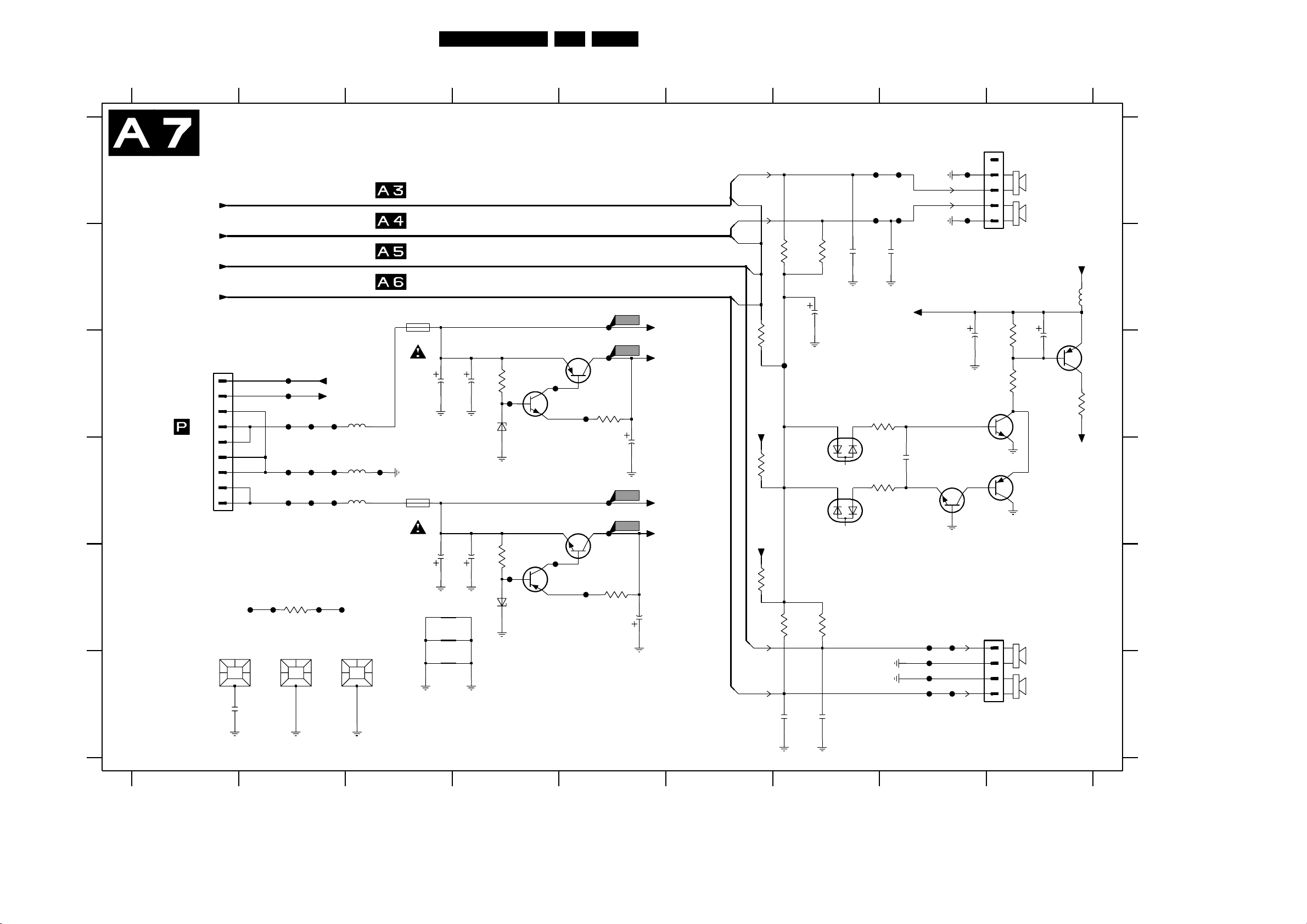
Electrical Diagrams and PWB Layouts
Audio Panel & Supply: Supply and DC Protection
33FM242 AB 7.
A
B
C
D
E
F
F730 = 14V4
F735 = 9V
F740 = -14V4
F745 = -8V8
8003 OF
1
2
SUPPLY & DC PROTECTION
FROM DIAGRAM
FROM DIAGRAM
FROM DIAGRAM
FROM DIAGRAM
SUPPLY
0302
PH-S
9
FROM
8
7
6
5
4
3
2
1
F796
0305
SHIELDING 3.3
10n
2799
12
F710
F711
F712
F713
F717
F718
F724
F723
RES=RESERVED
F797
3799
RES
0390
SHIELDING 3.3
DC_PROT
+9V_STBY
F714
F719
F725
F799
F798
SHIELDING 3.3
5714
100MHZ
5719
100MHZ
5725
100MHZ
0391
3456789
F772
F774
2753
BC847BW
7761
BC857BW
0303
PH-S
5
4
3
2
1
7751
0304
PH-S
4
3
2
1
10u
NC.
LEFT HIGH
LEFT LOW
47K
3752
2752
8V7
47K
BC857BW
3751
8V6
RIGHT HIGH
RIGHT LOW
8 Ohm
+9V_STBY
5753
10u
-0V2
7753
3754
DC_PROT
8 Ohm
CL 36532011_023.eps
F720
AUDIO AMPLIFIER LEFT HIGH
AUDIO AMPLIFIER LEFT LOW
AUDIO AMPLIFIER RIGHT HIGH
AUDIO AMPLIFIER RIGHT LOW
1730
T2.5AL 250V
1740
T2.5AL 250V
2730
2740
C704
C703
C702
220u
220u
2732
2742
GND_O
220u
F732
220u
F742
3732
9V8
6732
3742
-9V7
6742
2K7
BZX384-C10
2K7
BZX384-C10
7735
BC869
+14V4
F736
7736
BC847BW
9V2
-14V4
F746
7746
BC857BW
-9V2
13V7
F733
7745
BC868
-13V7
F743
-8V8
9V
3733
1K
3743
1K
F730
F735
2734
F740
F745
1u
2744
VSND_POS
VCC_10_POS
VSND_NEG
VCC_10_NEG
1u
OUT_PROT
OUT_PROT
OUT_PROT
DC PROTECTION
2771
GND_O
2
3
F771
F776
1n
GND_O
+9V_STBYA
3750
470R
3760
470R
1
GND_O
GND_O
2770
OUT_LH
OUT_PROT
OUT_LL
OUT_RH
OUT_RL
3770
10K
3749
VCC_10_POS
3755
100K
VCC_10_NEG
3765
100K
3780
2780
GND_O
100K
2760
F759
6750
BAV99W
6760
BAV99W
100K
1n
3771
3781
2781
GND_O
100K
22u
132
100K
1n
F770
F777
1n
2759
GND_O
GND_O
1n
F780
F782
F784
F786
7755
BC847BW
F781
F787
3456789
100MHZ
1K
200303
A
B
C
D
E
F
0302 C1
0303 A8
0304 E8
0305 E1
0390 E2
0391 E3
1730 B3
1740 D3
2730 C3
2732 C4
2734 D5
2740 E3
2742 E4
2744 E5
2752 C9
2753 C8
2759 D8
2760 B7
2770 B8
2771 B7
2780 F7
2781 F7
2799 F1
3732 C4
3733 C5
3742 E4
3743 E5
3749 C6
3750 C8
3751 C9
3752 C9
3754 C9
3755 D6
3760 D8
3765 E6
3770 B7
3771 B7
3780 E7
3781 E7
3799 E2
5714 C3
5719 D3
5725 D3
5753 B9
6732 C4
6742 E4
6750 D7
6760 D7
7735 C5
7736 C4
7745 D5
7746 E4
7751 C8
7753 C9
7755 D8
7761 D9
C702 F3
C703 E3
C704 E3
F710 C2
F711 C2
F712 C2
F713 C2
F714 C2
F717 D2
F718 D2
F719 D2
F720 D3
F723 D2
F724 D2
F725 D2
F730 B5
F732 C4
F733 C5
F735 C5
F736 C4
F740 D5
F742 E4
F743 E5
F745 D5
F746 E4
F759 C7
F770 A8
F771 A8
F772 A8
F774 A8
F776 A8
F777 A8
F780 E8
F781 E8
F782 F8
F784 F8
F786 F8
F787 F8
F796 E2
F797 E2
F798 E2
F799 E2
Page 34
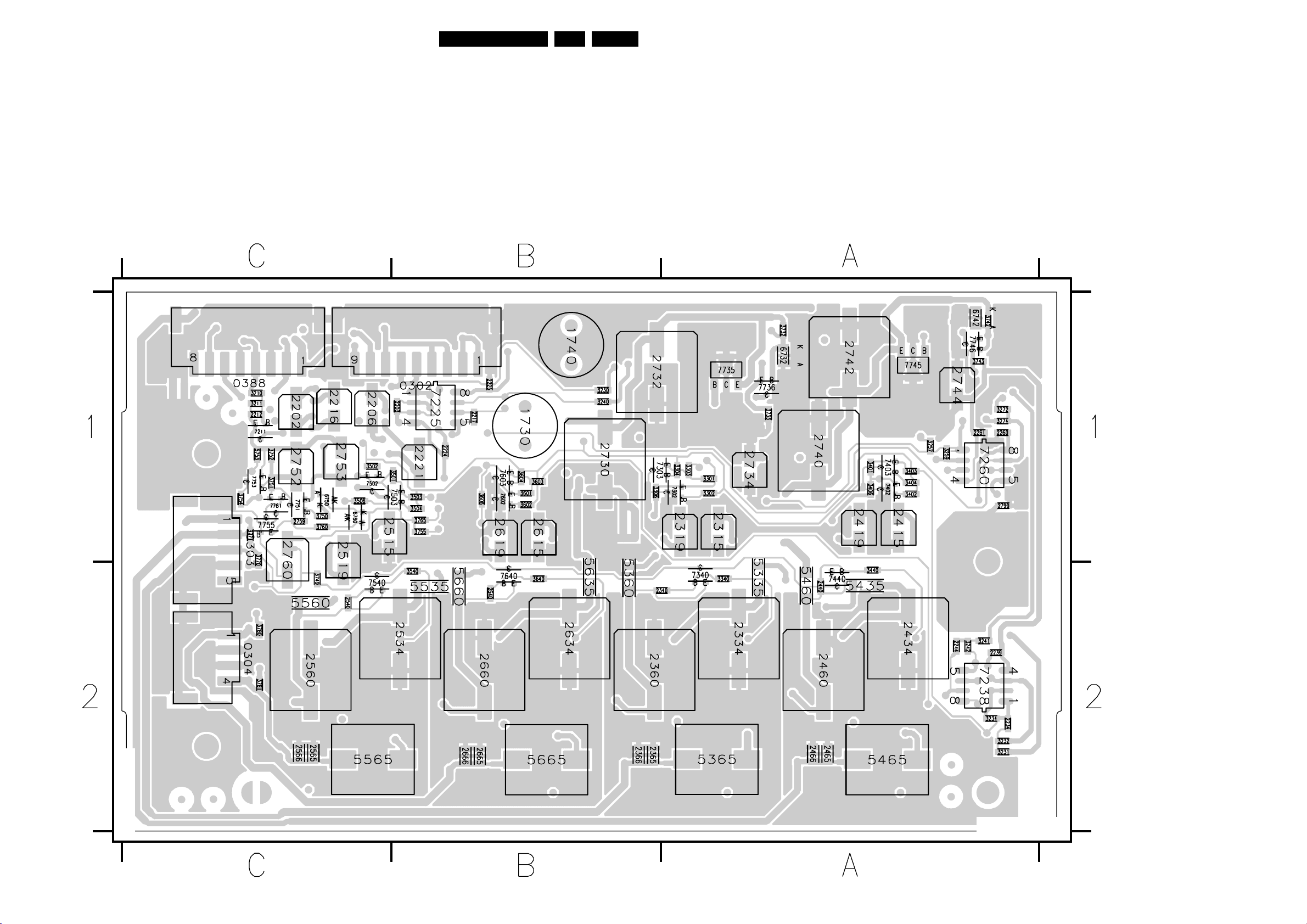
Electrical Diagrams and PWB Layouts
Layout Audio Panel (Top Side)
34FM242 AB 7.
0302 B1
0303 C1
0304 C2
0388 C1
1730 B1
1740 B1
2202 C1
2203 B1
2206 C1
2212 C1
2216 C1
2217 B1
2221 B1
2224 B1
2225 B1
2234 A2
2239 A2
2244 A2
2260 A1
2261 A1
2315 A1
2319 A1
2334 A2
2340 A2
2360 B2
2365 B2
2366 B2
2415 A1
2419 A1
2434 A2
2440 A2
2460 A2
2465 A2
2466 A2
2515 C1
2519 C1
2534 B2
2540 C2
2560 C2
2565 C2
2566 C2
2615 B1
2619 B1
2634 B2
2640 B2
2660 B2
2665 B2
2666 B2
2730 B1
2732 B1
2734 A1
2740 A1
2742 A1
2744 A1
2752 C1
2753 C1
2759 C1
2760 C1
2799 A1
3210 C1
3211 C1
3230 B1
3231 A2
3232 A2
3234 A2
3240 B1
3241 A2
3242 A2
3257 A1
3259 A1
3272 A1
3274 A1
3301 A1
3302 A1
3303 A1
3304 A1
3306 B1
3340 A2
3401 A1
3402 A1
3403 A1
3404 A1
3406 A1
3440 A2
3501 B1
3502 C1
3503 B1
3504 B1
3506 C1
3540 B2
3601 B1
3602 B1
3603 B1
3604 B1
3606 B1
3640 B2
3732 A1
3733 A1
3742 A1
3743 A1
3749 C2
3750 C1
3751 C1
3752 C1
3754 C1
3755 B1
3760 C1
3765 B1
3770 C1
3771 C1
3780 C2
3781 C2
5335 A2
5360 B2
5365 A2
5435 A2
5460 A2
5465 A2
5535 B2
5560 C2
5565 C2
5635 B2
5660 B2
5665 B2
5753 C1
6732 A1
6742 A1
6750 C1
6760 C1
7211 C1
7225 B1
7238 A2
7260 A1
7302 A1
7303 B1
7340 A2
7402 A1
7403 A1
7440 A2
7502 C1
7503 B1
7540 C2
7602 B1
7603 B1
7640 B2
7735 A1
7736 A1
7745 A1
7746 A1
7751 C1
7753 C1
7755 C1
7761 C1
CL 26532038_022.eps
150402
Page 35
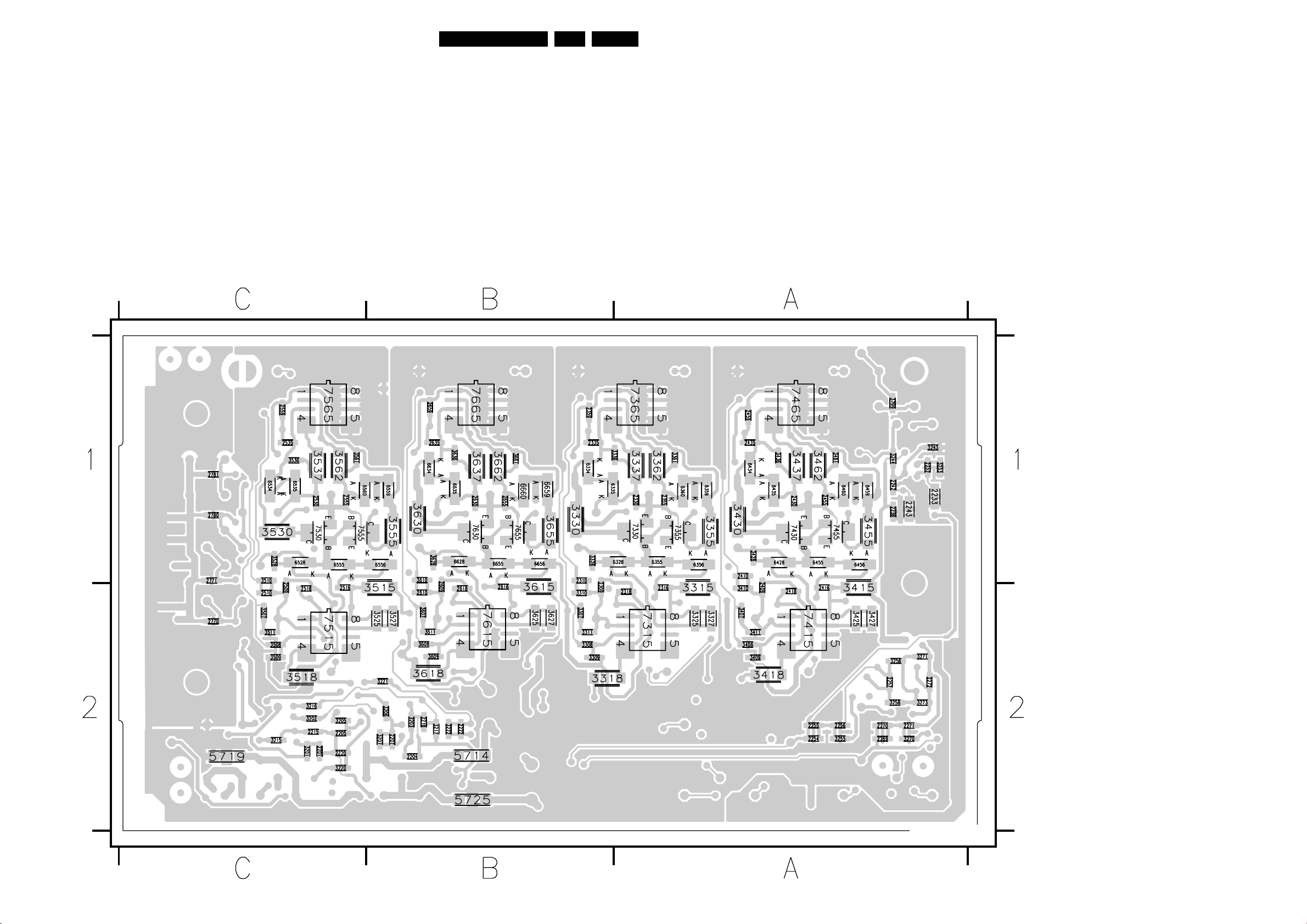
Electrical Diagrams and PWB Layouts
Layout Audio Panel (Bottom Side)
35FM242 AB 7.
2201 C2
2204 B2
2205 C2
2207 B2
2215 C2
2218 B2
2220 C2
2222 B2
2232 A1
2233 A1
2238 A1
2242 A1
2243 A1
2254 A2
2255 A2
2256 A2
2257 A2
2269 A2
2270 A2
2271 A2
2272 A2
2309 B2
2310 B1
2316 A2
2318 A2
2330 A1
2335 B1
2355 A1
2359 B1
2409 A2
2410 A1
2416 A2
2418 A2
2430 A1
2435 A1
2455 A1
2459 A1
2509 C2
2510 C2
2516 C2
2518 C2
2530 C1
2535 C1
2555 C1
2559 C1
2609 B2
2610 B2
2616 B2
2618 B2
2630 B1
2635 B1
2655 B1
2659 B1
2770 C2
2771 C1
2780 C1
2781 C1
3201 C2
3202 C2
3203 B2
3205 C2
3206 B2
3207 B2
3215 C2
3216 C2
3217 B2
3220 C2
3221 B2
3222 B2
3233 A1
3243 A1
3244 A1
3255 A2
3256 A2
3258 A2
3270 A2
3271 A2
3273 A2
3307 B2
3308 B2
3309 B2
3310 B2
3311 B2
3315 A2
3318 B2
3325 A2
3327 A2
3328 B1
3330 B1
3336 A1
3337 A1
3355 A1
3361 A1
3362 A1
3407 A2
3408 A2
3409 A2
3410 A2
3411 A2
3415 A2
3418 A2
3425 A2
3427 A2
3428 A1
3430 A1
3436 A1
3437 A1
3455 A1
3461 A1
3462 A1
3507 C2
3508 C2
3509 C2
3510 C1
3511 C2
3515 B2
3518 C2
3525 B2
3527 B2
3528 C1
3530 C1
3536 C1
3537 C1
3555 B1
3561 C1
3562 C1
3607 B2
3608 B2
3609 B2
3610 B1
3611 B2
3615 B2
3618 B2
3625 B2
3627 B2
3628 B1
3630 B1
3636 B1
3637 B1
3655 B1
3661 B1
3662 B1
3799 A1
5714 B2
5719 C2
5725 B2
6328 A1
6334 B1
6335 B1
6355 A1
6356 A1
6359 A1
6360 A1
6428 A1
6434 A1
6435 A1
6455 A1
6456 A1
6459 A1
6460 A1
6528 C1
6534 C1
6535 C1
6555 C1
6556 B1
6559 B1
6560 C1
6628 B1
6634 B1
6635 B1
6655 B1
6656 B1
6659 B1
6660 B1
7315 A2
7330 A1
7355 A1
7365 A1
7415 A2
7430 A1
7455 A1
7465 A1
7515 C2
7530 C1
7555 C1
7565 C1
7615 B2
7630 B1
7655 B1
7665 B1
CL 26532038_023.eps
150402
Page 36
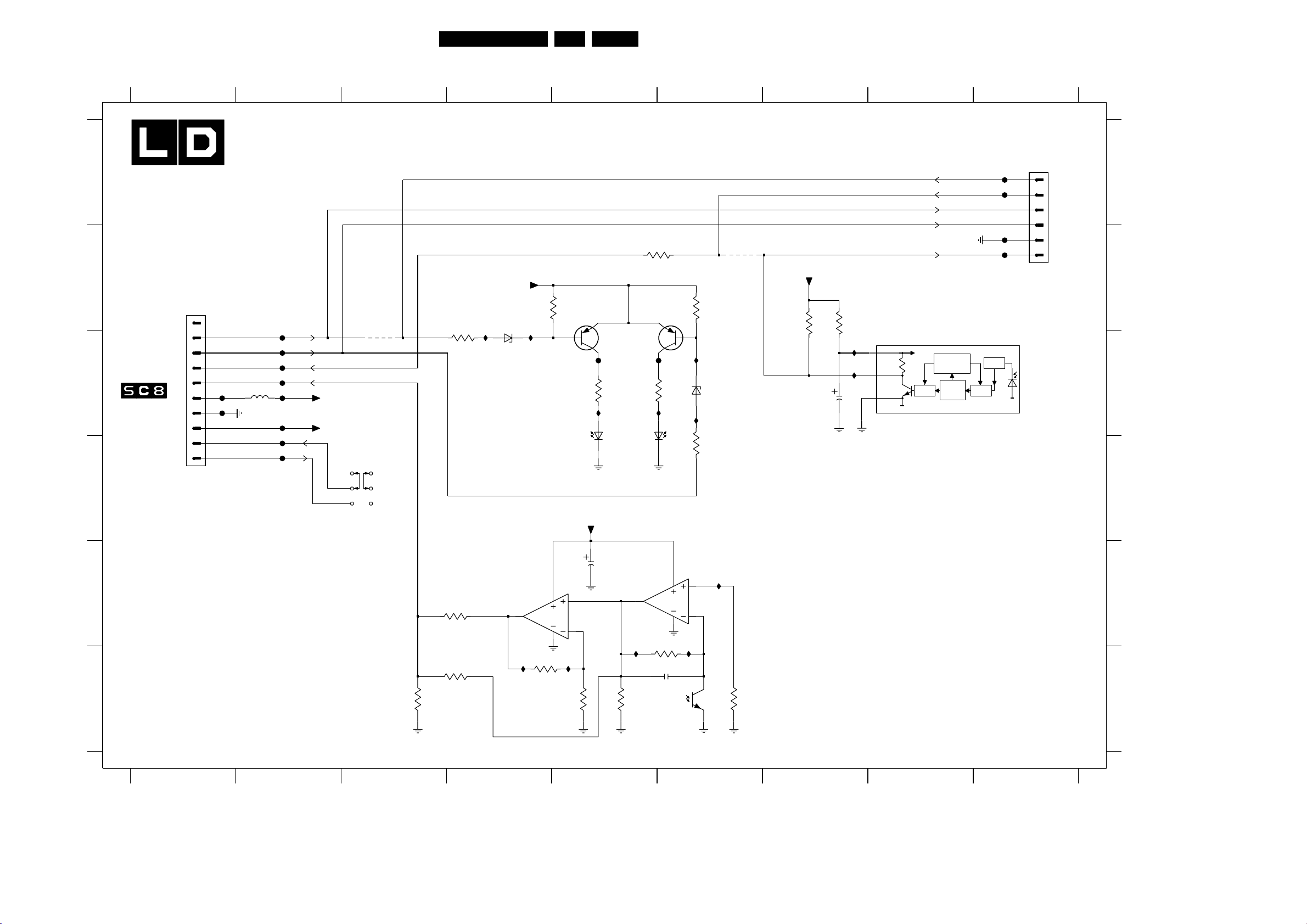
Electrical Diagrams and PWB Layouts
LED/Switch Panel (for Sets with Speakers)
123456789
LED/SWITCH PANEL
A
B
0320
1
C
CONTROLE
FUNCTIONS
D
E
F
FROM
0320
2
GREEN_LED
3
RED_LED
4
5
6
10
7
8
9
PH-S
RC_IN
LIGHT_SENSOR_IN
F106
F107
+5V_STBY_SW
+9V_STBY_SW
+9V_STBY
5100
100MHZ
F102
F103
F104
F105
F101
F108
F109
F112
+8V6
+5V_STBY_SW
1101
14
25
36
ON / OFF
SWITCH
4101
3122
1K
3101
150R
3120
4K7
3121
4K7
+5V_STBY_SW
6101
I102
BZX384-C3V9
7120-B
LM358D
7
I120 I123
I103
3123
10K
3102
8
4
7103
100K
BC857BW
6103-A
GREEN
+8V6
2120
5
6
3124
3103
1K
36FM242 AB 7.
F110
220R
I104
21
TLMV3100
10u
3125
7105
BC857BW
I105
RED
7120-A
LM358D
1
I125
3K3
3107
470R
F111
3105
3
6103-B
3126
470K
2126
220n
330R
4
TLMV3100
8
4
I126
6127
3104
6105
3106
3
2
100K
I106
I107
4107
BZX384-C3V9
150R
I127
3127
470K
TEMD5000
+5V_STBY_SW
10K
3108
3109
2107
100R
I109
I111
100u
0317 A9
0320 B1
1101 D3
2107 C7
2120 E5
2126 F6
3100 C2
3101 C4
3102 B4
3103 C5
3104 B6
3105 C5
3106 D6
3107 B6
3108 B7
3109 B7
3120 E4
3121 F4
3122 F3
3123 F4
3124 F5
3125 F5
3126 F6
3127 F6
4101 C3
4107 B6
6101 C4
6103-A C5
6103-B D5
6105 C6
6127 F6
7103 B5
7105 B5
7107 C9
7120-A E6
7120-B E4
F101 C2
F102 C2
F103 C2
F104 C2
F105 C2
F106 C1
F107 C1
F108 C2
F109 D2
F110 C5
F111 C6
F112 D2
F115 A9
F116 A9
F119 B9
F120 B9
I102 B4
I103 B4
I104 C5
I105 C5
I106 C6
I107 C6
I109 C7
I111 C7
I120 F4
I123 F5
I125 E5
I126 E6
I127 E6
LED_DISPLAY
IR_TX
GREEN_LED
RED_LED
IR_RX
F115
F116
F119
F120
1
2
3
4
5
6
0317
A
ICONN
for
ITV only
95009
B
RC RECIEVER
2
VS
1
OUT
3
GND
DEM
CTRL
CIRCUIT
BAND
PASS
TSOP2236
INP
AGC
PIN
7107
C
D
E
F
123
LIGHT SENSOR
CL 16532099_038.EPS
280901
456789
Page 37
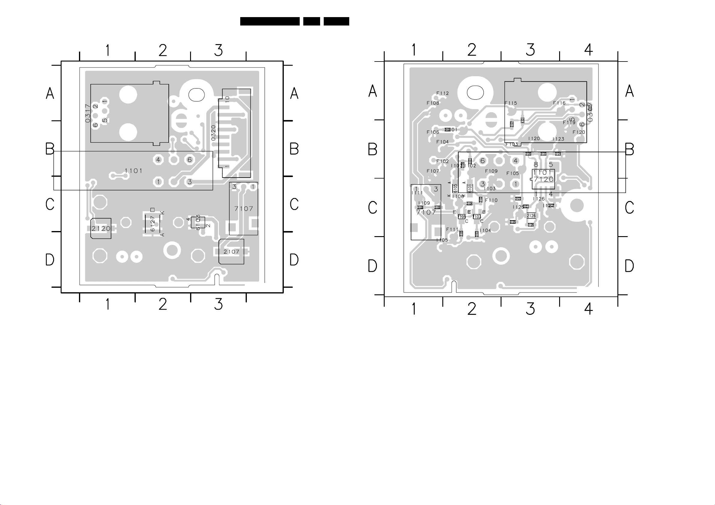
Electrical Diagrams and PWB Layouts
37FM242 AB 7.
Layout LED/Switch Panel (for Sets with Speakers) (Top Side)
0317 A1
0320 B3
1101 B1
2107 D3
2120 C1
6103 C3
6127 C2
7107 C3
Layout LED/Switch Panel (for Sets with Speakers) (Bottom Side)
0317 A4
1101 B3
2126 C3
3101 B2
3102 C2
3103 C2
3104 C2
3105 C2
3106 B2
3107 B3
3108 C1
3109 C1
3120 B3
3121 C3
3122 C3
3123 B3
3124 B3
3125 C3
3126 C3
3127 C3
4101 B3
4107 A4
5100 B2
6101 C2
6105 C2
7103 C2
7105 C2
7107 C1
7120 C3
CL 16532099_025.eps
240901
CL 16532099_024.eps
240901
Page 38
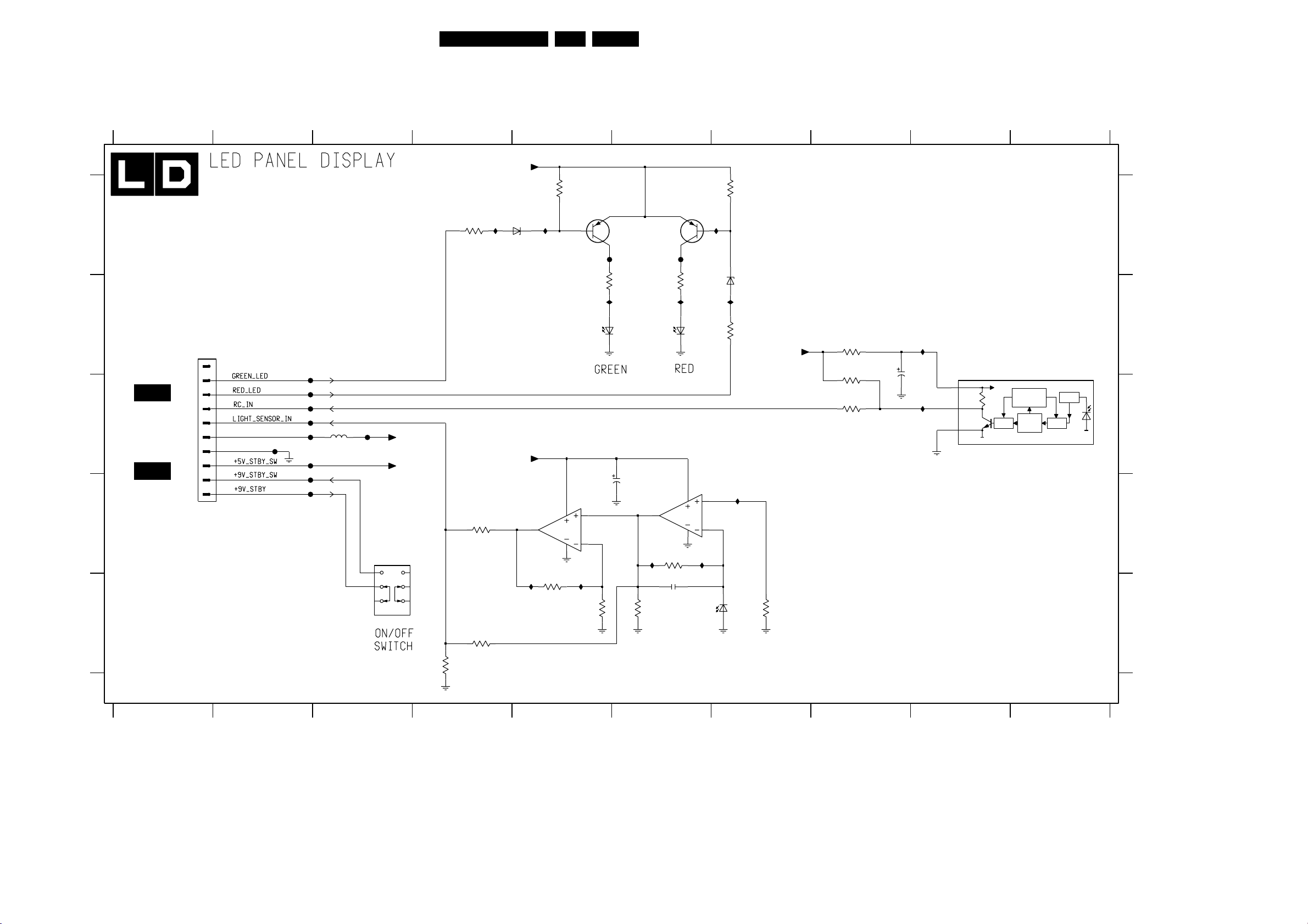
Electrical Diagrams and PWB Layouts
LED Panel Display (for Speakerless Sets)
1101 D3
1320 B1
2120 D5
2126 E6
3101 A4
3102 A52107 B8
3103 B5
3104 A7
3105 B6
3106 B7
3107 C8
3108 C8
3109 B8
3120 D4
3121 E4
3122 E4
3123 E5
3124 E5
3125 E6
3126 D6
3127 E7
5100 C2
6101 A5
6103-A B5
6103-B B6
6105 B7
6127 E7
7103 A5
7105 A6
7107 B10
7120-A D6
7120-B D5
F101 C2
F102 C2
F103 C2
38FM242 AB 7.
F104 C2
F105 C2
F106 C2
F107 C2
F108 C2
F109 D2
F110 A5
F111 A6
F112 D2
I102 A4
I103 A5
I104 B5
I105 B6
I106 A7
I107 B7
I109 B9
I111 C9
I120 E5
I123 E5
I125 D6
I126 D6
I127 D7
A
B
FROM
SC8
CONTROL
C
FUNCTIONS
EMC
EMC FILTER
PANEL
D
E
3122 123 6014.1
123
1320
1
0320
OR
1320
PH-S
2
3
4
5
6
7
8
9
10
F107
F102
F103
F104
F105
F106
F108
F109
F112
5100
100MHZ
F101
1
2
3
+8V6
+5V_STBY_SW
1101
SPPJ3
8
7
4
+5V_STBY_SW
I102
3101
150R
3120
4K7
4
5
6
3121
4K7
1K0
3122
6101
BZX384-C3V9
+8V6
567891
I103
7120-B
LM358D
7
I120
3123
10K
3102
100K
7103
BC857BW
F110
1K0
3103
I104
21
6103-A
TLMV3100
35V10u
2120
5
8
6
4
I123
1K0
3124
3125
7105
BC857BW
F111
3105
I105 I107
34
6103-B
7120-A
LM358D
1
I125
3126
470K
2126
220n
3K3
1K0
TLMV3100
8
4
I126
3
2
I106
6127
3104
100K
6105
BZX384-C3V9
3106
150R
I127
TEMD5000
+5V_STBY_SW
3127
470K
3109
100R
3108
10K
3107
470R
2107
16V100u
I109
I111
7107
TSOP2136
VS2
OUT1
GND3
DEM
CTRL
CIRCUIT
BAND
PASS
INP
AGC
PIN
CL 26532100_009.eps
A
B
C
D
E
140703
1
2
34567891
Page 39
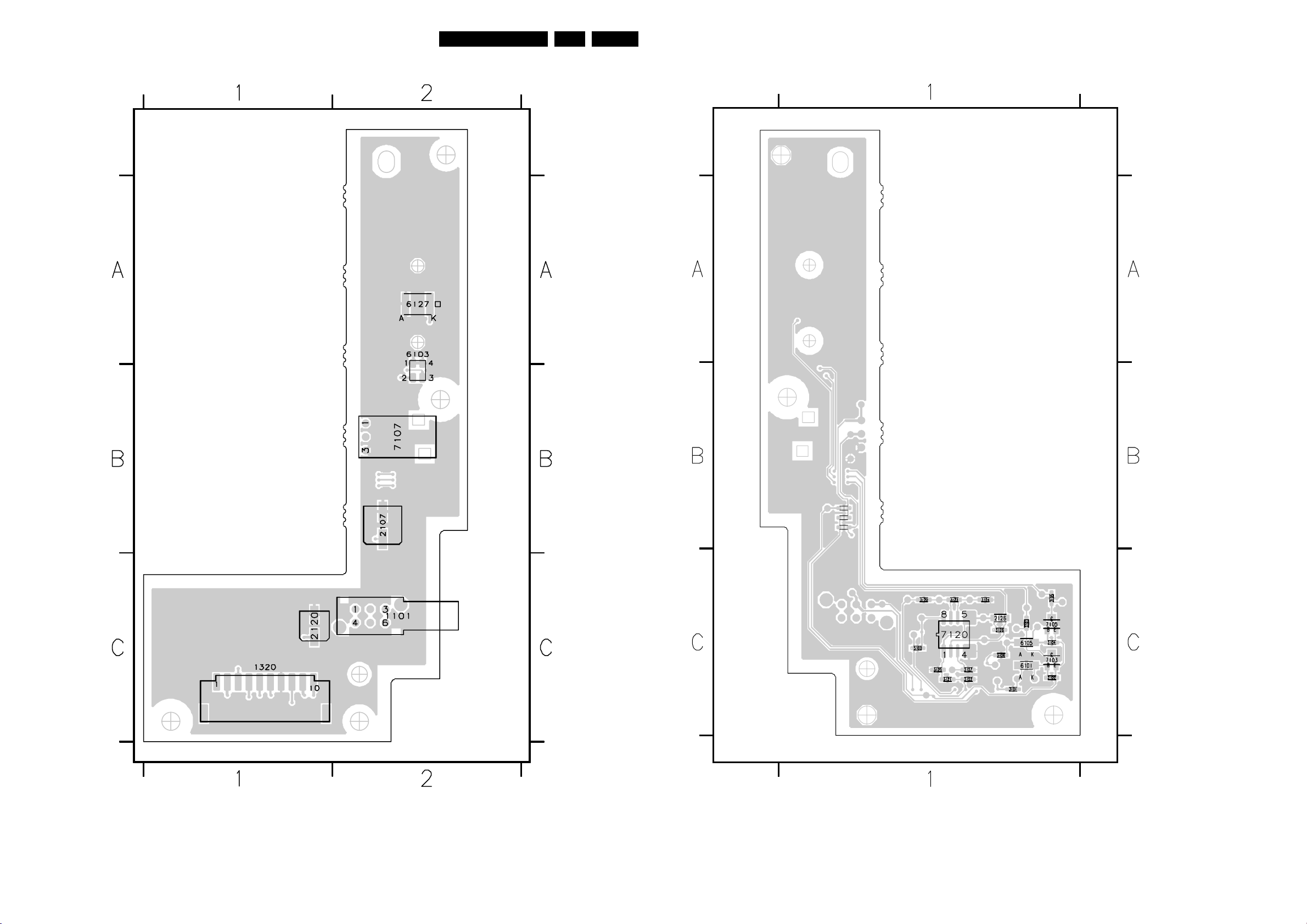
Electrical Diagrams and PWB Layouts
39FM242 AB 7.
Layout LED Panel Display (for Speakerless Sets) (Top Side)
1101 C 2
1320 C1
2107 B2
2120 C1
6103 A2
6127 A2
7107 B2
Layout LED Panel Display (for Speakerless Sets) (Bottom Side)
2126 C1
3101 C1
3102 C1
3103 C1
3104 C1
3105 C1
3106 C1
3107 B1
3108 B1
3109 B1
3120 C1
3121 C1
3122 C1
3123 C1
3124 C1
3125 C1
3126 C1
3127 C1
5100 C1
6101 C1
6105 C1
7103 C1
7105 C1
7120 C1
3122 123 6014.1
CL 26532100_010.eps
140703
3107
3108
3109
3122 123 6014.1
3120
5100
3123 3124
3125 3127
3122 3101
3121
3105
3103
3126
3106
3104
3102
CL 26532100_011.eps
140703
Page 40
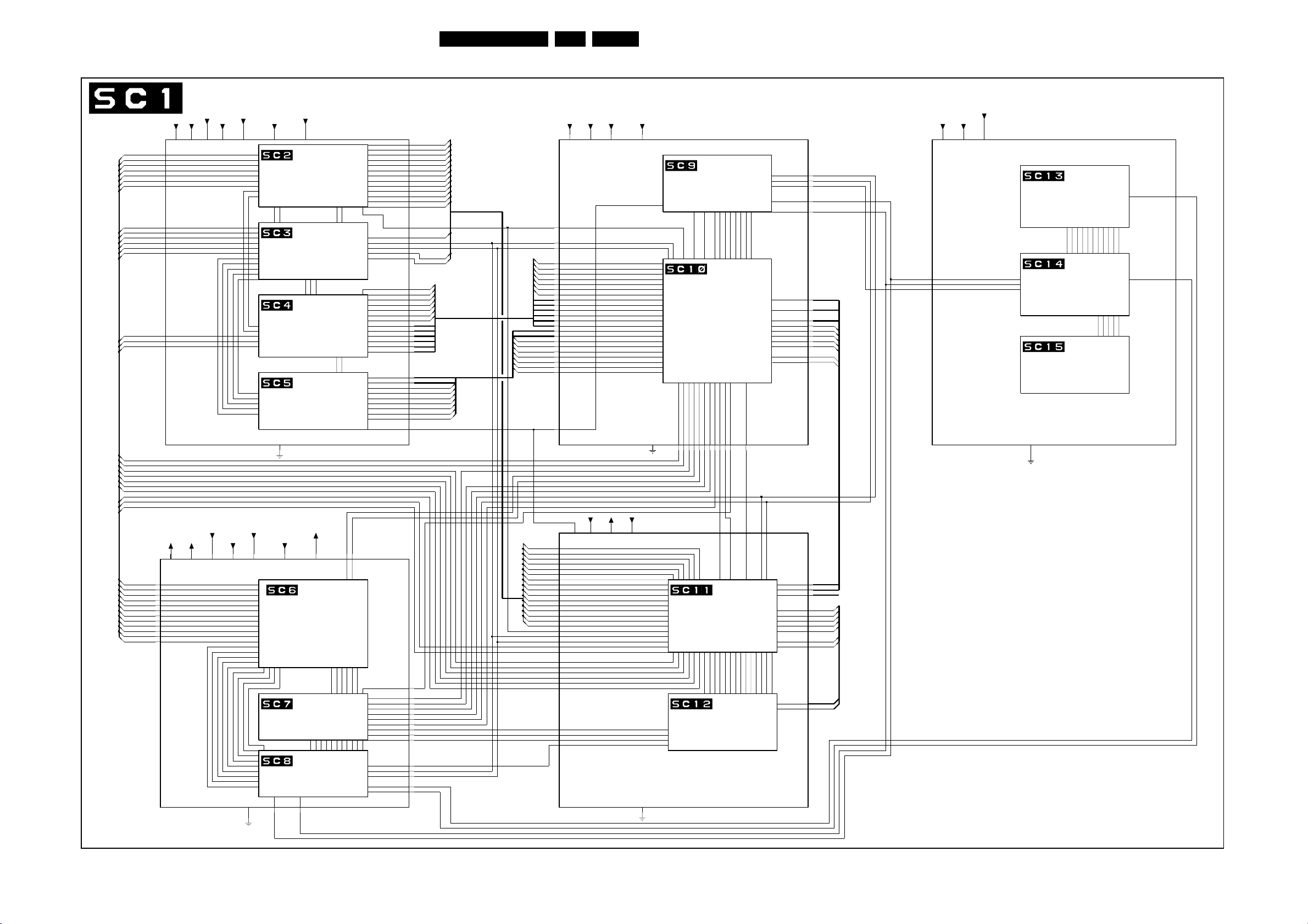
Electrical Diagrams and PWB Layouts
SCAVIO Panel: Function Blocks and Diagram Connections
40FM242 AB 7.
VGA2_OUTN
VGA1_H
VGA1_V
VGA2_H
VGA2_V
VGA2_EN
VGA2_OUT
VGA1_R
VGA1_G
VGA1_B
VGA2_R
VGA2_G
VGA2_B
GR_CLK
GR_ADDE
ALT_GR_ADDE
VGA2_EN
VGA2_OUT
VGA1_V
VGA1_H
GR_CLK
GR_ADDE
ALT_GR_ADDE
TV_MODE
VGA2_V
VGA2_H
TV_MODE
VGA1_R
VGA1_G
VGA1_B
VGA2_R
VGA2_G
VGA2_B
VGA2_OUTN
VGA1_H
VGA1_V
VGA2_H
VGA2_V
SCAVIO PANEL (FUNCTION BLOCKS AND DIAGRAM CONNECTIONS)
VREF1
+5V_STBY_SW
+8V6 +2V5
+3V3
+5V
VREF1
+3V3
VGA2_OUTN
VGA1_H
VGA1_V
VGA2_H
VGA2_V
VGA2_EN
VGA2_OUT
VGA1_R
VGA1_G
VGA1_B
VGA2_R
VGA2_G
VGA2_B
GR_CLK
ALT_GR_ADDE
VIDEO_SELECTION_AND_AQUISITION
+5V_POW
+3V3
+5V
+3V3 +3V3_STBY_SW+5V +5V_POW +5V_STBY_SW+8V6 +9V_STBY
TV_MODE
VGA1_R
VGA1_G
VGA1_B
VGA2_R
VGA2_G
VGA2_B
VGA2_OUTN
VGA1_H
VGA1_V
VGA2_H
VGA2_V
SELECT_2
SELECT_1
SELECT_3
MAIN_CONTROL
CBYSCVBS
CR
+8V6
SELECT_4
IR_TX
RL_ICN
V_ADC
H_ADC
Y_SYNC
+9V_STBY
IR_RX
GL_ICN
LD_ICN
GND
+3V3_STBY_SW
+3V3_STBY_SW+5V +5V_POW+5V_STBY_SW+8V6
+5V_POW
SYNC-PROCESSING
V_HD_EXT
H_HD_EXT
VIDEO SELECTION MATRIX
VIDEO SELECTION ADC
VIDEO DECODER
GND
+3V3_STBY_SW
+5V_STBY_SW
SDA_SW
SDA_SW
Y_HD
VIDEO_SEL_1
B_ADC
G_ADC
R_ADC
PW_SCL
PW_SDA
TXD_PW
TXD_PW
VGA-INPUT
RS_232_ACT
RXD_OTC
RC
TXD_OTC
CONTROL-FUNCTIONS
ICONN_ON
GRN_LED
FAN_SP_1
POWER_OK
LIGHT_SEN_IN
PSU_PROT
STANDBY
RED_LED
CONTROL_FUNCTIONS
SCL_SW
SCL_SW
RXD_PW
RXD_PW
UART_ACT
SYNC_ACT
PSU_IRQ
FAN_SP_2
V_SYNC_POL_N
V_SYNC_TTL
H_SYNC_POL_N
H_SYNC_TTL
V_SYNC_CMP
H_SYNC_CMP
C_SYNC_OUT
MATRIX_SEL
VIDEO_SEL_1
VIDEO_SEL_2
HD_CLAMPN
CLKOUT_DEINT
VOUT_DEINT
HOUT_DEINT
VFIELD_DEC
PW_FLASH_RESET
RC
POWER_DOWN
VIDEO_SEL_1
VIDEO_SEL_2
MSP_RESET
75OHM_ON
V_SYNC_LM
C_SYNC_LM
H_PRESENT
H_HD
V_HD
SYNC_SEL
HD_BLANKN
ADHS
GCLK
ADVS
ADSOG
ADDE
GCOAST
GBLKSPL
GRE(0:7)
GGE(0:7)
GBE(0:7)
GRO(0:7)GR_ADDE
GGO(0:7)
GBO(0:7)
Y_OUT(0:7)
UV_OUT(0:7)
PW_SCL
PW_SDA
VPEN
VIDCLK
PW_START
SDA_2
SCL_2
SDA_1
SCL_1
PW_RESET
IRQ_PDP
CPU_GO
PDP_GO
POWER_OK
V_SYNC_POL_N
V_SYNC_TTL
H_SYNC_POL_N
H_SYNC_TTL
75OHM_ON
V_SYNC_CMP
H_SYNC_CMP
V_SYNC_LM
C_SYNC_LM
C_SYNC_OUT
H_PRESENT
H_HD
V_HD
SYNC_SEL
MATRIX_SEL
VIDEO_SEL_1
VIDEO_SEL_2
HD_BLANKN
HD_CLAMPN
ADHS
GCLK
ADVS
ADSOG
ADDE
GCOAST
GBLKSP
GRE(0:7)
GGE(0:7)
GBE(0:7)
GRO(0:7)
GGO(0:7)
GBO(0:7)
Y_OUT(0:7)
UV_OUT(0:7)
PW_SCL
PW_SDA
CLKOUT_DEINT
VOUT_DEINT
HOUT_DEINT
VFIELD_DEC
VIDCLK
PW_FLASH_RESET
PW_START
SDA_2
SCL_2
SDA_1
SCL_1
PW_RESET
IRQ_PDP
CPU_GO
PDP_GO
POWER_DOWN
VIDEO_SEL_1
VIDEO_SEL_2
MSP_RESET
POWER_OK
VPEN
SYNC_SEL
ADSOG
GCLK
ADVS
ADDE
ADHS
GCOAST
GBLKSP
GRE(0:7)
GGE(0:7)
GBE(0:7)
GRO(0:7)
GGO(0:7)
GBO(0:7)
Y_OUT(0:7)
UV_OUT(0:7)
PW_SCL
PW_SDA
CLKOUT_DEINT
VPEN
VOUT_DEINT
HOUT_DEINT
VFIELD_DEC
HD_CLAMPN
HD_BLANKN
V_SYNC_POL_N
V_SYNC_TTL
H_SYNC_POL_N
H_SYNC_TTL
75OHM_ON
V_SYNC_CMP
H_SYNC_CMP
V_SYNC_LM
C_SYNC_LM
C_SYNC_OUT
H_PRESENT
H_HD
V_HD
MATRIX_SEL
VGA1_V
VGA1_H
GR_CLK
GR_ADDE
ALT_GR_ADDE
TV_MODE
SYNC_SEL
VIDEO_SEL_1
VIDEO_SEL_2
ADSOG
GCLK
ADVS
ADDE
ADHS
GCOAST
GBLKSPL
GRE(0:7)
GGE(0:7)
GBE(0:7)
GRO(0:7)
GGO(0:7)
GBO(0:7)
Y_OUT(0:7)
UV_OUT(0:7)
PW_SCL
PW_SDA
CLKOUT_DEINT
VPEN
VOUT_DEINT
HOUT_DEINT
VFIELD_DEC
VIDCLK
VIDCLK
HD_CLAMPN
HD_BLANKN
V_SYNC_POL_N
V_SYNC_TTL
H_SYNC_POL_N
H_SYNC_TTL
75OHM_ON
V_SYNC_CMP
H_SYNC_CMP
V_SYNC_LM
C_SYNC_LM
C_SYNC_OUT
H_PRESENT
H_HD
V_HD
MATRIX_SEL
SYNC_SEL
VIDEO_SEL_1
VIDEO_SEL_2
VGA2_V
VGA2_H
VGA1_V
VGA1_H
GR_CLK
GR_ADDE
ALT_GR_ADDE
TV_MODE
IRQ_PDP
CPU_GO
PDP_GO
POWER_DOWN
BACK_END
+3V3
+3V3_STBY_SW
+2V5+3V3 +3V3_STBY_SW+5V
SCALER_AND_CONTROL
+2V5
+3V3
+8V6
+2V5+3V3 +8V6
GND
GND
VGA2_EN
VGA2_OUT
BACK-END LVDS-OUTPUT
SCALER-CLOCK-GENERATOR
DCKEXT
BOOTWE
MCLK
ROMWE
A(0:19)
SCALER-PW164
SCL_2
SYNC
SDA_2
PW_RESET
SYNC
ROMOE
+MEMORY
1_2FH
PW_FLASH_RESET
1_2FH
D(0:15)
RXD_PW
PW_START
TXD_PW
BACK-END EPLD
B_OUT(0:7)
G_OUT(0:7)
H_SYNC_OUT
BLANK_OUT
V_SYNC_OUT
R_OUT(0:7)
PARITY_OUT
PW_RESET
PW_SDA_NVM
PW_SCL_NVM
FBX_MODE
FBX_MODE
SDA_1
FBX_MODE
DCLK
SCL_1_3V3
SDA_1
SCL_1
VXCA_18M432
SCL_1
POWER_DOWN_EPLD
SDA_1_3V3
PWRDWN_LVDS
SDA_1
SCL_1
SDA_SW
SCL_SW
DRE(0:7)
DGE(0:7)
DBE(0:7)
PARITY
DCLK
PW_SDA
PW_SCL
DRE(0:7)
DGE(0:7)
DBE(0:7)
PARITY
DCLK
PW_SDA
PW_SCL
PW_SDA
PW_SCL
DEN
DHS
DVS
DEN
DHS
DVS
SDA_1
SCL_1
VXCA_18M432
SDA_SW
SCL_SW
DRE(0:7)
DGE(0:7)
DBE(0:7)
PARITY
DEN
DHS
DVS
DCLK
PW_SDA
PW_SCL
DRE(0:7)
DGE(0:7)
DBE(0:7)
PARITY
DEN
DHS
DVS
DCLK
PW_SDA
PW_SCL
PW_SDA
PW_SCL
+5V
+8V6+5V
+5V +8V6 +9V_STBY
SDA_SW
SCL_SW
VXCA_18M432
AUDIO_PROCESSOR_FUNCTION
+9V_STBY
SOURCE_SELECT
POWER_OK
PRE_OUT1_L
D_CTR_NIL
PRE_OUT2_R
SC1_R
SCL_AUDIO
PRE_OUT2_L
SDA_AUDIO
SC1_L
PRE_OUT1_R
D_CTR_ONE
AUDIO_ENABLE
AUDIO PROCESSOR
MSP_RESET
I2S_CLOCK
I2S_DATA_IN2
I2S_DATA_IN1
I2S_DATA_OUT
MSP_RESET
AUDIO_DELAY_LINE
GND
3122 123 6001.7
CL 36532051_014.eps
200603
Page 41
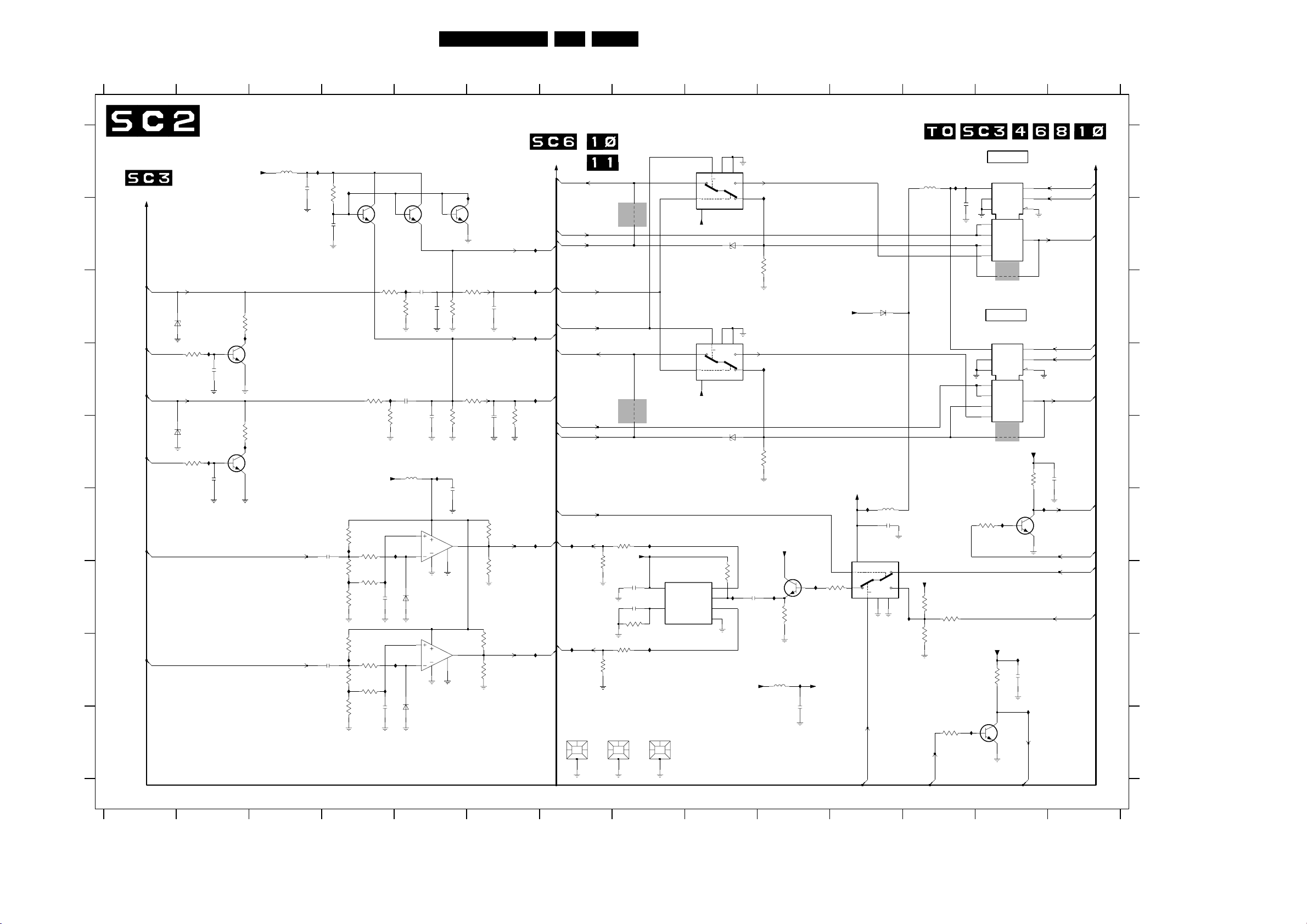
Electrical Diagrams and PWB Layouts
SCAVIO Panel: Sync Selection & Switching
1
234567891011121314
SYNC SELECTION
& SWITCHING
(ENHANCED ONLY UNLESS INDICATED OTHERWISE)
A
B
C
D
E
F
G
H
I
3122 123 6001.7
12345
V_HD_EXT
75OHM_ON
H_HD_EXT
75OHM_ON
6001
6010
BZM55-C33
I008
3006
10K
BZM55-C33
I013
3015
10K
BC847BW
2004
BC847BW
2005
+5V
100MHZ
75R
3001
7006
I007
2u2
75R
3010
7010
I012
2u2
5000
V_HD_EXT
H_HD_EXT
I000
2000
I002
100n
3000
470K
100n
2001
3020
2021
470n
3022
I023 I024
3030
2030
470n
3031
I034 I035
3032 3023
I019
I031
100K
2K2
22K
100K
2K2
22K
100R
3021
4K7
3024
100K
3033
4K7
3034
100K
BC847BW
3011
+5V
2022
2034
3002
100R
I010
3012
I018
I030
100n
10n
I005
3003
2012
100n
4K7
100MHZ
6034 6022
5020
2002
2u2
4K7
9
10
BAT254
4
5
BAT254
70017000
BC847BW
2008
2015
I014
11
6
11
6
47p
47p
7025-B
LM319D
GND
7025-A
LM319D
GND
3004
3013
2020
8
3
470K
470K
7
12
220K
220K
100n
VGA2_V
I003
7002
BC847BW
V_HD
I004
I006
I009
I011
I020
I032
VGA1_V
VGA2_OUTN
VGA2_EN_NOT
VGA2_H
H_HD
VGA1_H
H_PRESENT
C_SYNC_LM
I021
V_SYNC_LM
I029
SHIELDING 3.3
1001
3005
3014
3035
3036
3026
3025
2003
2014
1K
2K2
1K
2K2
100n
10n
3008
V_SYNC_TTL
V_SYNC_POL_N
H_SYNC_TTL
H_SYNC_POL_N
470K
V_SYNC_CMP
H_SYNC_CMP
67
41FM242 AB 7.
3041
2K2
3K3
3040
3043
2K2
3K3
3044
SHIELDING 3.3
1002
4006
BASICBASIC
4007
+5B
2040
100n
2041
100n
3042
220K
RES
RES
I017
SYNC. SLICER
8
VS
7
O|E-FI
6
RSET
5
BG|BP
I027
SHIELDING 3.3
1003
7007-A
74HCT4053D
14
11
7007-C
74HCT4053D
4
9
LM1881M
CSYNC
VSYNC
Z
S
+5A
Z
S
+5A
Vdd
Vdd
7040
GND
6
E
16
6
E
16
1
2
VIN
3
4
8
Vee7Vss
Y1
Y0
6019
BZX384-C2V4
7
8
Vee Vss
Y1
Y0
6007
BZX384-C2V4
RES
3045
470K
I039
I038
13
I041
12
3019
10K
10
15
+5A
16
Vdd
S
Z
6009
BAT254
I001
100MHZ
7007-B
74HCT4053D
E
Vee7Vss
6
VGA2_EN_NOT
5007
2007
100n
8
3
5
+5V
2042
100n
I040
3007
10K
I025
5060
100MHZ
+5B
3051
7041
BC847BW
1K
I033
2060
I022
+5B
100n
+5V
3050
1K
5009
100MHZ
Y0
2
+5B
Y1
1
1K
3052
3053
3054
2K2
1K
3060
10K
VGA2_EN
I026
2009
100n
I037
SWITCH
7009-A
74HC4052D
16
VCC
7
VEE
GND
1
MDX
0
5
1
2
2
4
3
BASIC
4010
SWITCH
7009-B
74HC4052D
16
VCC
7
VEE
8
GND
12
MDX
0
14
1
15
2
11
3
BASIC
4009
I016
3065
10K
+3V3_STBY_SW
4K7
3061
7060
BC847BW
10
0
9
1
68
G4
3
10
0
9
1
6
G4
13
+3V3_STBY_SW
3066
I015
7065
BC847BW
I028
100n
2061
I036
VGA2_EN_NOT
8 9 10 11 12 13 14
VIDEO_SEL_2
SYNC_SEL
V_ADC
VIDEO_SEL_2
SYNC_SEL
H_ADC
1K0
2066
100n
VGA2_OUTN
VGA2_OUT
Y_HD
C_SYNC_OUT
CL 36532051_015.eps
140703
1001 I7
1002 I7
1003 I8
2000 A3
2001 B4
2002 C5
2003 C6
2004 D2
2005 E2
2007 F11
2008 C5
2009 B12
2012 D5
2014 E6
A
2015 E5
2020 F5
2021 F4
2022 G4
2030 H4
2034 I4
2040 G8
2041 G8
2042 G9
2060 I10
2061 H13
B
2066 E14
3000 A4
3001 C2
3002 C4
3003 C5
3004 C5
3005 C6
3006 D2
3007 E10
3008 E6
3010 E2
3011 D4
C
3012 E4
3013 E5
3014 D6
3015 E2
3019 B9
3020 F4
3021 F4
3022 G4
3023 G4
3024 G4
3025 G6
3026 F6
D
3030 H4
3031 H4
3032 I4
3033 H4
3034 H4
3035 H6
3036 H6
3040 G7
3041 F8
3042 G8
3043 H8
E
3044 H7
3045 G9
3050 G11
3051 G10
3052 G12
3053 H12
3054 G12
3060 I12
3061 H13
3065 F13
3066 E13
4006 B8
F
4007 D8
4009 E13
4010 C13
5000 A3
5007 F11
5009 A12
5020 E5
5060 H10
6001 C1
6007 E9
6009 C11
6010 E1
G
6019 B9
6022 G5
6034 I5
7000 B4
7001 B5
7002 B6
7006 C2
7007-A A9
7007-B F11
7007-C C9
7009-A A13
H
7009-B C13
7010 E2
7025-A H5
7025-B F5
7040 G9
7041 G10
7060 I13
7065 F13
I000 A3
I001 F11
I002 A4
I003 B6
I
I004 B6
I005 C5
I006 C6
I007 C3
I008 D2
I009 D6
I010 D4
I011 D6
I012 E3
I013 E2
I014 E5
I015 F13
I016 F13
I017 F8
I018 F5
I019 F4
I020 F6
I021 F7
I022 G10
I023 G4
I024 G4
I025 G10
I026 G11
I027 H8
I028 H13
I029 H7
I030 H5
I031 H4
I032 H6
I033 H10
I034 H4
I035 H4
I036 H13
I037 I12
I038 A12
I039 G9
I040 D10
I041 A10
Page 42
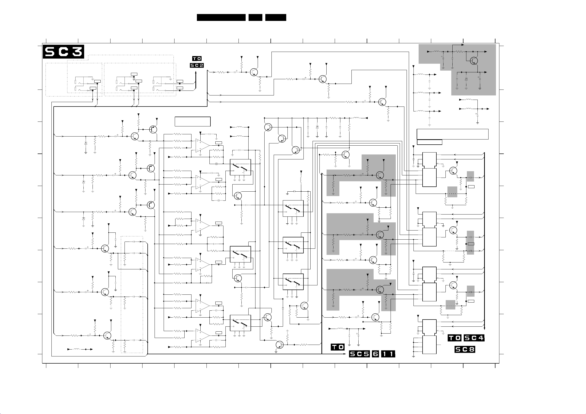
Electrical Diagrams and PWB Layouts
SCAVIO Panel: Video Selection & Matrix
123
VIDEO-SELECTION & MATRIX
0377 SPEAKERLESS VERSION
CVBS + Y INPUT
ONE BLOCK WITH
A
AUDIO_YC +
AUDIO_CVBS
ON SC 13
NOT FOR SPEAKERLESS
B
C
D
Y
PR
E
PB
F
Y
G
PR
H
I
PB
3122 123 6001.7
+5V
12345678
G/Y/Y
CVBS
3112
270R
3116
270R
3120
270R
5170
100MHZ
I073
I081
I086
0379-A
COMBI
6071
6076
6091
2112
2116
I135
2
3
1
BZM55-C33
BZM55-C33
VREF1A
22u
VREF1B
22u
2120
22u
F070
F073
Y
3071
BZM55-C33
3077
270R
75R
3076
3082
270R
75R
3081
22K
3113
I074
22K
3117
I082
VREF1B
3121
I087
+5M
3072
270R
75R
7113
BC847BW
7117
BC847BW
22K
BC847BW
0380-C
COMBI
R/PR/Cr
B/PB/Cb
NOT FOR SPEAKERLESS
VREF1A
3073
2072
I051
22u
VREF1B
22K
3078
2077
I059
I067
+5M
+5M
7121
3115
3119
+5M
22u
2082
22u
I076
I084
3123
VREF1B
2113
1K
2117
1K
I088
I060
22K
3083
I068
100n
3195
100n
3194
1K
3193
8
9
7
7074
22K
BC847BW
I052
7079
BC847BW
7084
BC847BW
1K
1K
1K
CLOSE TO 7118
IN LAYOUT
ONE BLOCK WITH
AUDIO_RGB
ON SC 13
F076
F071
F074
PR
PB
+8A
3074
220R
I050
I053
+8A
BC857BW
3079
220R
I057
I062
+8A
BC857BW
3084
220R
I066
I069
2118
Y_SYNC
47n
2115
YS
47n
Y_HD
2119
CR
47n
2123
CB
47n
CVBS
42FM242 AB 7.
4 5 6 7 8 9 1011121314
+8A
3164
470R
100n
I099
6166
100n
2166
BASIC+ENHANCED
+5V
100MHZ
+8V6
+8SW
1K0
3129
3133
+8SW
1K0
3130
3162
+8SW
1K0
3131
3166
100R
I101
7165
BC847BW
2167
BZX384-C2V4
5166
5167
RES
2168
VIDEO_SEL_2
VIDEO_SEL_1
B+E
R_ADC
2146
47n
F146
100R
VIDEO_SEL_2
VIDEO_SEL_1
B+E
G_ADC
2152
47n
F152
SOGIN
2151
1n
100R
VIDEO_SEL_2
VIDEO_SEL_1
B+E
2158
B_ADC
47n
F158
VIDEO_SEL_2
VIDEO_SEL_1
CL 36532051_016.eps
14
7075
BC857BW
3075
7080
3080
560R
7085
3085
560R
I100
(ENHANCED ONLY UNLESS INDICATED OTHERWISE)
7135
22K
BC847BW
I103
F089
16
Vdd
E
6
7102
BC847BW
2109
220n
1K
16
Vdd
E
6
7103
BC847BW
2110
220n
1K
16
Vdd
E
6
S
Z
S
10
Z
15
S
11
Z
14
+8A
BC847BW
9
4
3136
7110
3178
I104
560R
I143
BC847BW
10K
I142
I140
I090
BC847BW
7111
7104
BC847BW
1K
3180
7105
I137
BC847BW
74HCT4053D
Y0
2
Y1
1
8
74HCT4053D
Y0
5
Y1
3
8
74HCT4053D
Y0
12
Y1
13
8
I138
2111
3181
3137
270R
7112
I148
220n
7100-B
Vee7Vss
7100-C
Vee7Vss
7100-A
Vee7Vss
3183
10K
2108
100n
10K
I150
I145
I105
E
6
E
6
E
6
3184
I149
+8V6
16
Vdd
16
Vdd
16
Vdd
5180
10K
3182
2137
22u
100MHZ
S
10
Z
15
S
Z
S
11
Z
14
10K
VREF1A
2107
3186
9
4
22K
BC847BW
3138
I106
6105
100n
10K
7107
PMBT2369
HD_BLANKN
MATRIX_SEL
7138
BZX384-C2V4
I147
HD_CLAMPN
+8V6
+8A
2106
3176
10K
VGA1_R
VGA2_R
VGA1_G
VGA2_G
VGA1_B
VGA2_B
I107
3139
560R
3140
270R
I144
3175
1K
2u2
3170
I146
3173
100R
3147
270R
2105
10K
100n
3144
270R
I117
3174
BASIC+ENHANCED
3150
270R
3171
100R
I123
3153
270R
BASIC+ENHANCED
3156
270R
3172
100R
I129
3159
270R
I113
5140
100MHZ
2142
I109
5175
100MHZ
1K
7115
PMBT2369
I114
VREF1C
2147
22u
I120
VREF1C
2153
22u
I126
2159
22u
2143
100n
2140
22u
VREF1C
2144
22u
3148
I118
VREF1C
2150
22u
3154
I124
VREF1C
2156
22u
VREF1C
3160
I131
100u
VREF1B
3145
7148
22K
BC847BW
3151
7154
22K
BC847BW
3157
22K
BC847BW
+8AA
3141
+8V6
I115
I121
I127
7160
22K
3V0
22K
3V0
22K
3V0
7141
22K
BC847BW
I110
7145
BC847BW
+8AA
3149
7151
BC847BW
+8AA
3155
7157
BC847BW
+8AA
3161
+8AA
560R
560R
+8A
3146
I119
3152
I125
3158
560R
3142
+8AA
560R
3190
560R
3189
+8AA
560R
3188
560R
B+E
I116
I122
2V4
I128
2V4
2V4
I111
220R
220R
220R
+8SW
2145
+8SW
2157
VREF1
5160
100MHZ
5161
100MHZ
5162
100MHZ
100n
1
5
2
4
+8SW
12
14
15
11
100n
1
5
2
4
+8SW
12
14
15
11
VREF1B
3135
2134
7
7
14
3097
390R
2097
3126
3K9
14
8
8
1%
1p
3118
4K7
3089
1K5
2114
2127
3107
3K9
3128
4K7
2128
3111
2K2
1p0
680R
1p0
1p0
I054
I058
3124
2K2
3093
2124
1p0
I065
I072
I078
I083
3134
270R
I102
+8V6
+5V
1%
1%
22u
100MHZ
74HCT4053D
Y0
5
Y1
3
8
I141
74HCT4053D
Y0
2
Y1
1
I139
74HCT4053D
Y0
12
Y1
13
5089
5090
RES
2089
100n
7089-C
Vee7Vss
7089-B
Vee8Vss
7
7089-A
Vee8Vss
7
3177
3179
0380-B
COMBI
5
V
H
+8A
F072
6
4
F075
V_HD_EXT
H_HD_EXT
PB
Y
PR
MATRIX
+8A
2088
100n
5
4
7088-A
TSH93
6
11
+8A
2090
+8A
+8A
+8A
TSH93
TSH93
TSH93
TSH93
4
11
4
11
4
11
4
11
7090-A
7088-C
1%
1%
7090-C
3103
330R
2103
1p
7088-B
100n
5
6
12
13
12
13
10
9
1%
+8A
10
9
TSH93
4
11
1%
7090-B
560R
+8A
+8A
VREF2
VREF2
VREF2
VREF2
VREF2
VREF2
1%
3114
1%
4K7
3086
1K5
I055
3087
820R
I056
3088
820R
3122
2K2
3090
680R
I061
3091
1%
330R
I063
3092
1%
330R
3094
1%
1K
3125
1%
4K7
I064
3095
1K2
3096
470R
1%
I070
3098
1%
1K
3099
1%
1K
I071
3100
1%
1K5
3101
680R
I075
3102
1K8
1%
3127
1%
4K7
I077
3104
1%
3K9
3105
1%
1K8
I079 I130
3106
1%
1K8
I080
3108
2K2
3109
1K2
I085
3110
1K2
5164
+8V6
100MHZ
100u
2164
2165
I108
VREF1A
2160
I133
VREF1B
2161
100n 100n
I134
VREF1C
100n
2162
VIDEO-SELECTION
4 X SWITCH
7146-A
74HC4052D
16
7
8
1
16
7
8
1
16
7
1
16
7
1
VCC
VEE
GND
0
2
3
74HC4052D
VCC
VEE
GND
0
2
3
74HC4052D
VCC
VEE
GND
0
2
3
74HC4052D
VCC
VEE
GND
0
2
3
MDX
MDX
MDX
MDX
G4
7146-B
G4
7158-A
G4
7158-B
G4
10
0
9
1
6
7129
BC847BW
3
BASIC
4146
RES
3132
220R
10
0
9
1
6
7130
BC847BW
13
4152
RES
3163
220R
10
0
9
1
68
7131
BC847BW
3
BASIC
4158
RES
3165
220R
10
0
9
1
68
13
9 10111213
3V3
2V6
I112
0377 A2
0379-A A2
0380-B A4
0380-C A3
A
B
C
D
E
F
G
H
I
2072 C3
2077 D3
2082 E3
2088 C6
2089 C7
2090 D6
2097 F6
2103 G6
2105 C10
2106 C9
2107 C9
2108 E8
2109 E7
2110 H7
2111 H8
2112 F2
2113 F3
2114 D6
2115 G3
2116 H2
2117 H3
2118 F3
2119 H3
2120 I2
2123 I3
2124 E6
2127 H6
2128 I6
2134 A6
2137 A9
2140 B10
2142 I10
2143 I10
2144 D10
2145 D12
2146 D14
2147 E10
2150 F10
2151 F14
2152 F14
2153 G10
2156 H10
2157 G12
2158 H14
2159 I10
2160 A12
2161 B12
2162 B12
2164 A13
2165 A13
2166 A13
2167 A14
2168 B14
3071 C2
3072 C2
3073 C3
3074 C3
3075 C4
3076 D2
3077 D2
3078 D3
3079 D3
3080 D4
3081 E2
3082 E2
3083 E3
3084 E3
3085 F4
3086 C5
3087 C5
3088 D5
3089 D6
3090 D5
3091 D5
3092 E5
3093 E6
3094 E5
3095 F5
3096 F5
3097 F6
3098 F5
3099 G5
3100 G5
3101 G5
3102 G5
3103 G6
3104 H5
3105 H5
3106 I5
3107 I6
3108 I5
3109 I5
3110 I5
3111 I6
3112 F1
3113 F2
3114 C5
3115 G2
3116 H1
3117 H2
3118 C6
3119 H2
3120 I1
3121 I2
3122 D5
3123 I3
3124 D6
3125 E5
3126 F6
3127 H5
3128 I6
3129 D13
3130 F13
3131 H13
3132 E13
VREF1
VREF2
100u
+8SW
10u
140703
3133 E14
3134 A6
3135 A7
3136 A7
3137 A8
3138 A9
3139 A9
3140 B10
3141 B11
3142 B11
3144 D10
3145 D10
3146 D11
3147 E10
3148 E10
3149 E11
3150 F10
3151 F10
3152 F11
3153 G10
3154 G10
3155 G11
3156 H10
3157 H10
3158 H11
3159 I10
3160 H10
3161 I11
3162 G13
3163 G13
3164 A13
3165 H13
3166 H13
3170 D9
3171 F9
3172 H9
3173 D9
3174 C10
3175 B9
3176 C9
3177 E7
3178 D7
3179 H7
3180 I7
3181 I8
3182 I9
3183 H8
3184 H8
3186 E9
3188 I11
3189 G11
3190 E11
3193 I3
3194 H3
3195 G3
4146 E13
4152 G13
4158 H13
5089 C7
5090 C7
5140 I10
5160 A12
5161 B12
5162 B12
5164 A13
5166 B14
5167 B14
5170 I1
5175 B10
5180 D8
6071 C2
6076 D2
6091 F2
6105 C9
6166 A14
7074 C3
7075 B4
7079 D3
7080 D4
7084 E3
7085 E4
7088-A C5
7088-B H5
7088-C F5
7089-A H7
7089-B F7
7089-C D7
7090-A D5
7090-B I5
7090-C G5
7100-A G8
7100-B E8
7100-C F8
7102 E7
7103 G7
7104 I8
7105 I8
7107 H9
7110 C7
7111 C8
7112 C8
7113 F2
7115 D10
7117 H2
7121 I2
7129 D13
7130 F13
7131 G13
7135 A7
7138 A9
7141 B11
7145 D11
7146-A C13
7146-B E13
7148 E10
7151 F11
7154 G10
7157 H11
7158-A G13
7158-B I13
7160 H11
7165 A14
F070 A2
F071 A3
F072 A5
F073 A2
F074 A3
F075 A5
F076 A3
F089 C7
F146 E14
F152 F14
F158 H14
I050 C4
I051 C2
I052 C3
I053 C4
I054 C6
I055 C5
I056 D5
I057 D3
I058 D6
I059 D2
I060 D3
I061 D5
I062 D3
I063 E5
I064 F5
I065 F6
I066 E3
I067 E2
I068 E3
I069 E3
I070 F5
I071 G5
I072 G6
I073 F2
I074 F2
I075 G5
I076 G3
I077 H5
I078 H6
I079 I5
I080 I5
I081 H2
I082 H2
I083 I6
I084 H3
I085 I5
I086 I2
I087 I2
I088 I3
I090 I7
I099 A13
I100 A13
I101 A14
I102 A6
I103 A7
I104 A7
I105 A8
I106 A9
I107 A10
I108 A12
I109 B10
I110 B11
I111 B11
I112 B14
I113 I10
I114 D10
I115 D11
I116 D11
I117 E10
I118 E10
I119 E11
I120 F10
I121 F11
I122 F11
I123 G10
I124 G10
I125 G11
I126 H10
I127 H11
I128 H11
I129 I10
I130 I11
I131 I10
I133 B13
I134 B13
I135 I2
I137 I8
I138 H8
I139 H6
I140 H7
I141 E6
I142 E7
I143 B7
I144 B10
I145 C8
I146 C10
I147 C9
I148 H8
I149 I8
I150 I8
Page 43
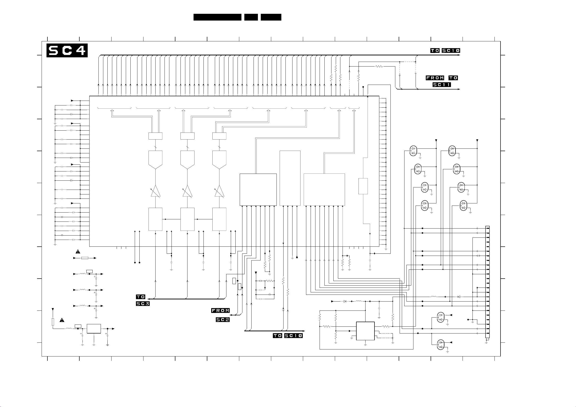
Electrical Diagrams and PWB Layouts
SCAVIO Panel: Video Selection ADC
12345678910
VIDEO-SELECTION
GRE(4)
GRE(3)
GRE(2)
GRE(1)
GRE(0)
A
7170
B
C
D
E
F
+3V3PLL
2171
100n
2173
100n
2174
100n
2176
100n
2178
100n
2180
100n
2182
100n
2184
100n
2185
100n
+3V3OUTPUT
2186
100n
2188
100n
2190
100n
2192
100n
G
H
+5V_POW
L 32V
1171
I
F 315mA
3122 123 6001.7
12345
+3V3MAIN1
100n
+3V3MAIN2
+3V3
+3V3_AD
+3V3_AD
+3V3_AD
5197
100MHZ
2170
100n
2172
100n
2175
100n
2177
100n
2179
2181
100n
2183
100n
2187
100n
2189
100n
2191
100n
2193
100n
100MHZ
100MHZ
100MHZ
F197
AD9887KS
1170
F 500mA
441
5196 F196
5198
5199
2195
PVD5
87 88
PVD4
79
PVD3
77
PVD2
75
PVD1
VD17
124 127
VD16
123
VD15
117
VD14
VD13
114 115
VD12
VD11
105 107
VD10
VD9
98 104
VD8
96
VD7
70
VD6
VD5
67 68
VD4
VD3
54 55
VD2
51
VD1
VDD8
141 151
VDD7
VDD6
43 132
VDD5
31
VDD4
VDD3
11 21
VDD2
1
VDD1
L 32V
F198
F199
7175
LD1117
IN3OUT
GND
10u
150
149
148
REDA0
REDA1
REDA2
AD-CONVERTER
+TMDS RECEIVER
+3V3_AD
+3V3MAIN1
10u
2196
+3V3OUTPUT
10u
2198
+3V3MAIN2
10u
2199
F162
2
1
2197
147
10u
146
REDA3
71
+3V3PLL
REDA4
NC1
GRE(5)
145
REDA5
NC2
72
GRE(6)
144
REDA6
NC3
73
GRE(7)
143
REDA7
GRE(0:7)
SCAN_IN129
F202
43FM242 AB 7.
-ADC
GRO(0:7) GBO(0:7)
GRO(0)
160
REDB0
GRO(1)
159
REDB1
158
REDB2
GRO(2)
GRO(3)
157
REDB3
8
GRO(4)
156
REDB4
A/D
GRO(5)
155
REDB5
154
REDB6
(BASIC AND ENHANCED VERSION)
GGE(0:7)
GGE(7)
GGE(6)
GGE(5)
GGE(4)
GGE(3)
GGE(2)
GGE(1)
GGE(0)
GRO(7)
GRO(6)
7
4
153
10
REDB7
GREENA09GREENA18GREENA2
GREENA36GREENA45GREENA5
8
3
GREENA6
GREENA720GREENB019GREENB118GREENB217GREENB316GREENB4
A/DCLAMP
GGO(0)
8
GGO(1)
A/D
GGO(0:7)
GGO(2)
GGO(3)
GGO(4)
15
GGO(6)
GGO(5)
14
GREENB5
GREENB613GREENB7
GBE(0:7)
GBE(1)
GBE(0)
GGO(7)
BLUEA030BLUEA129BLUEA228BLUEA3
GBE(2)
GBE(3)
27
GBE(5)
GBE(4)
BLUEA426BLUEA525BLUEA6
SYNC
AND CLOCK
GENERATION
PROCESSING
50 SCAN_CLK
F203
CLAMP
119 RAIN
0V3
R_ADC
RCLAMPV118
120 RMIDSCV
2205
I155
100n
GAIN110
0V3
G_ADC
GCLAMPV
GMIDSCV
109
111
I156
2206
100n
CLAMP
BAIN100
I157
0V3
B_ADC
SOGIN
101 BMIDSCV
2207
100n
BCLAMPV99
F210
H_ADC
82 HSYNC
F211
V_ADC
VSYNC81
108 SOGIN
GCOAST
GBLKSPL
CLAMP93
84 COAST
+3V3PLL
2208
39n
2209
RES
2211
RES
CKEXT83
I153
3207
3208
I158
2210
3n9
94 CKINV
3206
10K
3K3
I152
1K
FILT78
1V7
I159
6 7 8 9 1011121314
GBE(7)
GBE(6)
24
GBO(1)
GBO(0)
23
BLUEA7
BLUEB040BLUEB139BLUEB238BLUEB337BLUEB436BLUEB535BLUEB6
AND
POWER MANAGMENT
A189
SCL91
SDA92
90 A0
+3V3MAIN1
3209
100R
3210
100R
PW_SCL
PW_SDA
GBO(2)
RX0+62
GBO(3)
63 RX0-
GBO(4)
{ADSOG,ADVS,ADDE,ADHS,GCLK}
GBO(7)
GBO(6)
GBO(5)
34
33
BLUEB7
TMDS
RX2+56
RX2-57
RX1+
59
60 RX1-
+5V_STBY_SW
4K7
3214
3215
100R
ADVS
ADHS
ADSOG
3204
100R
3203
3205
100R
100R
4201
139
136
140
138
SCDT
VSOUT
HSOUT
SOGOUT
RECEIVER
RTERM53
65 RXC+
66 RXC-
I154
1K
3212
3211
6214
MCL4148
DDC-EPROM
4K7
RES
3213
F216
10K
3216
GCLK
134
DATACK
46 CTL0
1K
I160
3200
100R
F201
135DE137
DATACK_
CTL147
CTL248
5214
100MHZ
7215
ST24FC21
6
SCL5SDA
7
VCLK
3
DU
1V3
45
126REFOUT
SCAN_OUT
REF
REFIN125
CTL349
2212
I161
8
VCC
NC1
NC2
VSS
4
11 12 13 14
4200
6200
BAV99W
3
BAV99W
ADDE
4202
ALT_GR_ADDE
2
1
6201
3
6202
BAV99W
3
6203
BAV99W
3
F170
F171
F172
F173
F174
F175
F176
F177
F180
F181
+3V3
6204
BAV99W
2
3
1
6205
3
6209
BAV99W
3
I165
2
1
2
1
BAV99W
3
BAV99W
MCL4148
+3V3
+3V3
6206
3
BAV99W
6210
2
1
2
1
2
1
5210
100MHZ
6208
BAV99W
GND33
GND32
GND31
GND30
GND29
GND28
GND27
GND26
GND25
GND24
GND23
GND22
GND21
GND20
GND19
GND18
GND17
GND16
GND15
GND14
GND13
GND12
GND11
GND10
GND9
GND8
GND7
GND6
GND5
GND4
GND3
GND2
GND1
I151
100n
3219
RES
152
133 142
131
13022
128
122
121
113 116
106 112
102 103
95 97
86
85
76 80
74
69
61 64
52 58
42 44
32 41
12
2
100n
2217
3217
100R
1
4215
2
4216
4203
GR_CLK
GR_ADDE
{GR_CLK,GR_ADDE,ALT_GR_ADDE,TV_MODE}
4K7
3218
2
1
2
1
6207
2
3
1
RX2-
RX2+
SCL
SDA
RX1-
RX1+
I166
RX0-
RX0+
F178
RXC+
RXC-
CL 36532051_017.eps
+3V3
SOCKET
1
2
3
4
5
6
7
8
9
10
11
12
13
14
15
16
17
18
19
20
21
22
23
24
25
DVI
INPUT
0375
26
140703
I160 H10
0375 F14
I161 H11
1170 G2
I165 H13
1171 I1
I166 H14
2170 B1
2171 B1
2172 B1
2173 B1
2174 C1
2175 C1
2176 C1
2177 C1
2178 D1
2179 D1
2180 D1
A
2181 D1
2182 D1
2183 D1
2184 E1
2185 E1
2186 E1
2187 E1
2188 F1
2189 F1
2190 F1
2191 F1
B
2192 F1
2193 F1
2195 I2
2196 G2
2197 I2
2198 H2
2199 H2
2205 G4
2206 G5
2207 G6
2208 H7
2209 H7
C
2210 H7
2211 H7
2212 G11
2217 H11
3200 A10
3203 A9
3204 A9
3205 A10
3206 G7
3207 G7
3208 H7
3209 H8
D
3210 H8
3211 G10
3212 G10
3213 I9
3214 I9
3215 I9
3216 I9
3217 I11
3218 I11
3219 A11
4200 A12
E
4201 A10
4202 A12
4203 A11
4215 I11
4216 I11
5196 G2
5197 I1
5198 H2
5199 H2
5210 H13
5214 H10
6200 C12
F
6201 D12
6202 D12
6203 E12
6204 C13
6205 D13
6206 D13
6207 E13
6208 H13
6209 I13
6210 H13
6214 H10
7170 B2
G
7175 I2
7215 I10
F162 I2
F170 F12
F171 F12
F172 G12
F173 G12
F174 G12
F175 G12
F176 H12
F177 H12
H
F178 I14
F180 I12
F181 I12
F196 G2
F197 I1
F198 H2
F199 H2
F201 B10
F202 G3
F203 G3
F210 H6
F211 H7
I
F216 I10
I151 G11
I152 G8
I153 G7
I154 G10
I155 G5
I156 G6
I157 G6
I158 H7
I159 H8
Page 44
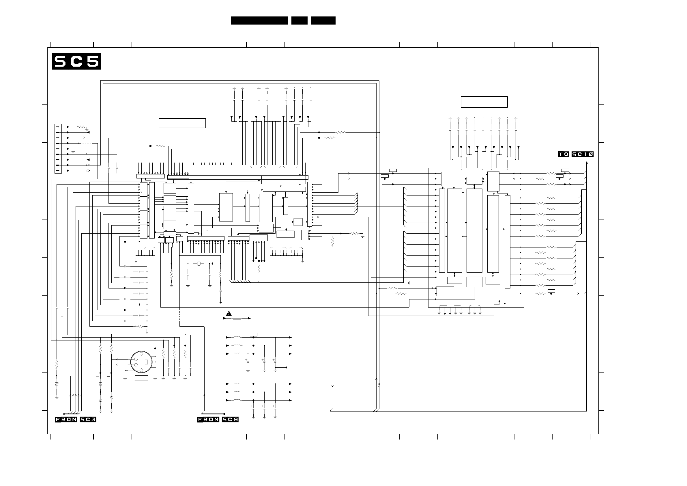
Electrical Diagrams and PWB Layouts
SCAVIO Panel: Video Selection Decoder
1 2345
VIDEO-SELECTION-DECODER
A
TO
3D COMB FILTER
0387
B
C
D
E
F
G
H
I
F225
3220
FSC
1
F226
RES
2
2274
3274
6274
F227
3
F228
4
F229
5
F230
6
F231
7
F232
8
F233
9
47n
2276
47n
2275
18R
BZM55-C33
8V6
C_OUT
CVBS1
+5V
PW_SDA
PW_SCL
47n
Y_SYNC
Y_OUT
CBYSCVBS
CR
+8V6
4220
3122 123 6001.7
1 2345678
+5V
I200
3275
F236
6276
6277
RES
2225
18R
3276
F235
BZM55-C33
6278
BZM55-C33
SAA7118E
RES
2226
F260
2260
47n
2262
47n
2264
47n
2266
47n
2268
47n
2270
47n
18R
Y
C
BZM55-C33
7225
M13 FSW
J2 A|11
K1 A|12
K2 A|13
L3 A|14
K3 A|1D
G4 A|21
G3
H2 A|23
J3 A|24
H1 A|2D
E3 A|31
F2 A|32
F3 A|33
G1 A|34
F1 A|3D
B1 A|41
D2 A|42
D1 A|43
E1 A|44
D3 A|4D
M1 AOUT
1
3
4
2
3V3DD
N6
N8
ADP0P8ADP1M7ADP2L7ADP3P7ADP4N7ADP5
CLKEXT
AD-PORT
+ ADC1
ANALOG1
A|22
+ ADC1
ANALOG1
+ ADC1
ANALOG1
ANALOG INPUT CONTROL
+ ADC1
ANALOG1
VSSA VSSE VSSI
AGNDL2AGNDA
VXSS
J4
A4
C2
H3E4C1
M2
2261
47n
2263
47n
2265
47n
2267
47n
2269
47n
3271
100R
F234
0381
YC Input
5
7
6
SVHS
VIDEO-DECODER
3225
4K7
N4
L6
P13
D13
C14
P5
CE
ADP6M6ADP7P6ADP8
TEST0
TEST1
TEST2
RESON
CONTROL
FAST
SWITCH
DELAY
COMP
PROC
CHROM
PROC
COMB
FIL
LUM
PROC
S
SYNC
GPO
RST0
RST1
M10
I205
3260
56R
2277
RTCO
N10
I201
3279
RES
RAW
XTAL
XTALB4XTALIA2XTOUT
L10
4K7
56R
2279
Y
CB
CR
CB
CR
A3
4250
Y
S
R
G
B
C
Y
S
VIDEO
CLK
LLCN5LLC2
P4
3277
P3
B13
B14
B2
A13
B12
A12
RES1
RES2
TEST5
EXMCLR
RES3C3RES4C4RES5
S
YCBCR
YCBCR
TEST3
TEST4
DECODER OUTPUT CONTROL
XRDY
XPD0B8XPD1A9XPD2B9XPD3
XPD4
XPD5
XPD6
A8
A6
A10
B10
1250
RES
RES
2252
2253
I202
56R
3278
RES
RES
2278
VIDCLK
C12
C13
RES6
RES7N1RES8N2RES9
IIC REGISTER MAP
RAW
YCBCRS
CBCR
XRHD8XRV
XCLKB7XDQ
XPD7
A7
C7
A11
C11
I207
RES
5226
I203
2254
+3V3
+3V3VID
+3V3VID
+3V3VID
+3V3_AD
+3V3_AD
+3V3_AD
6789
(ENHANCED VERSION ONLY)
2230
100n
3V3DD
N3
N13
N14
VXDD
RES12P2RES13
RES10
RES11
PRESCALER
BCS-SCALER
FIR-PREFILTER
H-PORTX-PORT
XTRI
HPD0
HPD1
HPD2
HPD3
B11
E11
E13
D14
RES
UV_DEC(3)
UV_DEC(2)
UV_DEC(1)
UV_DEC(0)
RES
1270
F 500mA
441
5221
100MHZ
5223
100MHZ
5228
100MHZ
5220
100MHZ
5222
100MHZ
5224
100MHZ
B3
VDDA4A
HPD4
E12
UV_DEC(4)
2232
2231
100n
100n
3V3AA
3V3AA
M3K4L1
H4
J1
F4
G2
E2
VDDA2A
VDDA3A
D4
VDDA VDDE VDDI
VDDA1A
1ST TASK IIC REG MAP SCALER
2ST TASK IIC REG MAP SCALER
SCALER EVENT CONTROLLER
LINE FIFO BUFFER
VERTICAL SCALING
VBI DATA
HPD6
HPD7
F13
F14
G13
UV_DEC(7)
UV_DEC(6)
BOUNDARY
SCAN
F261
F265
3261
+3V3VID
SLICER
TCKB5TDIA5TDO
TMSC6TRSTN
B6
F263
F262
470R
CBCR
HPD5
E14
UV_DEC(5)
L 32V
F221
F223
F237
10u
2228
2223
F220
F222
F224
10u
2224
2222
2240
100n
3V3DA
C5C9D12
HORIZONTAL FINE-
D6
F264
3V3DB
H12M4M8
M11C8C10
(PHASE-) SCALING
VIDEO/TEXT
ARBITER
L4
D5
D9
D11
G11
10u
10u
2221
I204
10u
10u
2220
2247
2248
100n
3V3DB
F12
J12
VIDEO FIFO
L8
D7
L11
D10
2249
2250
100n
100n
3V3DB
3V3DB
P9
N9
P10
M9
M5
SCL
SDA
INT_A
TEXT
OUTPUT FORMATTER I-PORT
FIFO
ASCLK N11
CLK
AUDIO
L5
L9
J11
F11
3V3DA
3V3DC
3V3DE
3V3AA
3V3DB
3V3DD
100n
IDP5
F250
F251
44FM242 AB 7.
10 11
12 13 14
DE-INTERLACER
2284
3250
3251
100R
100R
7280
F240
F241
K13IGP1
L14IGP0
K14IGPV
K12IGPH
G14IDP0
G12IDP1
H11IDP2
H14IDP3
H13IDP4
J14
J13IDP6
K11IDP7
M14ICLK
L13IDQ
N12ITRDY
L12ITRI
P12ALRCLK
P11AMCLK
M12AMXCLK
3262
Y_DEC(0)
Y_DEC(1)
Y_DEC(2)
Y_DEC(0:7)
Y_DEC(3)
Y_DEC(4)
Y_DEC(5)
Y_DEC(6)
Y_DEC(7)
I206
3263
RES
RES
F242
Y_DEC(0)
Y_DEC(1)
Y_DEC(0:7)
Y_DEC(2)
Y_DEC(3)
Y_DEC(4)
Y_DEC(5)
Y_DEC(6)
Y_DEC(7)
UV_DEC(0)
UV_DEC(1)
UV_DEC(0:7)
UV_DEC(2)
UV_DEC(3)
UV_DEC(4)
UV_DEC(5)
UV_DEC(6)
UV_DEC(7)
HDEC
VDEC
VPEN_DEC
SDA9400
23 HIN
22 VIN
29 SYNCEN
43 YIN0
44 YIN1
45 YIN2
46 YIN3
47 YIN4
48 YIN5
49 YIN6
50 YIN7
31 UVIN0
UVIN1
32
33 UVIN2
34 UVIN3
37 UVIN4
38 UVIN5
39 UVIN6
40 UVIN7
30 RESET
19 TEST
VFIELD_DEC
PW_SCL
PW_SDA
3284
100R
PW_SCL
3285
100R
21 SDA
20 SCL
CLK154
2280
100n
3V3DC
ISC
INP SYNC
CONTROLLER
LDR
VERTICEL
NOISE REDUCTION
MOTION
IFC INPUT FORMAT CONVERSION
AND PHASE
MOVIE MODE
LM
LINE MEM
I2C
-BUS
INTERFACE
VSS1
2 8 24 42 55 36 52
2283
2282
2281
100n
3V3DC
100n
3V3DC
100n
3V3DC
VDD2
MC
MEM CTRL
ED
eDRAM
DECIMATION
HORIZONTAL
INTERFACESDATA BUFFER
AND MEASUREMENT
DETECTOR
CONTROL
VOLTAGE
TEST
CTRL
DETECTION
PLL1
CLOCK
DOUBLING
VSS2
2285
100n
3V3DC
OSC
OUTP
SYNC
CONTR.
HDR
VERTICAL
LM
LINE MEM
X1|CLK227X2
58 28
100n
3V3DE
VDD1
SCAN RATE
INTERPOLATION
DOUBLING
9 101112
2288
2287
2286
41563551535759
100n
3V3DE
925
100n
3V3DE
100n
3V3DE
61VOUT|VEXT
60HOUT|HEXT
62HREF
18INTERLACED
7YOUT0
6YOUT1
5YOUT2
4YOUT3
3
YOUT4
CONVERSION
1YOUT5
64YOUT6
63YOUT7
17UVOUT0
16UVOUT1
15UVOUT2
14UVOUT3
OFC OUTPUT FORMAT CONVERSION
13UVOUT4
12UVOUT5
11UVOUT6
10UVOUT7
PLL2
CLOCK
26CLKOUT
3286-C
100R
3286-A
F247
F245
3286-B
F246
100R
100R
3289-B
100R
3289-D
100R
3290-B
100R
3290-D
100R
3291-B
100R
3291-D
100R
3292-B
100R
3292-D
100R
3293
100R
3289-A
100R
3289-C
100R
3290-A
100R
3290-C
100R
3291-A
100R
3291-C
100R
3292-A
100R
3292-C
100R
F249
Y_OUT(0)
Y_OUT(1)
Y_OUT(2)
Y_OUT(3)
Y_OUT(4)
Y_OUT(5)
Y_OUT(6)
Y_OUT(7)
UV_OUT(0)
UV_OUT(1)
UV_OUT(2)
UV_OUT(3)
UV_OUT(4)
UV_OUT(5)
UV_OUT(6)
UV_OUT(7)
CLKOUT_DEINT
CL 36532051_018.eps
13 14
VOUT_DEINT
HOUT_DEINT
VPEN
Y_OUT(0:7)
UV_OUT(0:7)
140703
0381 H3
0387 B1
1250 F4
1270 G5
2220 I6
2221 H6
2222 I6
2223 H6
2224 I6
2225 C2
2226 C2
2228 H5
2230 A5
A
2231 A5
2232 A6
2240 A6
2247 A6
2248 A7
2249 A7
2250 A7
2252 F4
2253 F4
2254 F5
2260 F2
2261 F3
B
2262 F2
2263 F3
2264 F2
2265 F3
2266 G2
2267 G3
2268 G2
2269 G3
2270 G2
2274 G1
2275 G1
2276 G1
C
2277 H3
2278 H4
2279 H4
2280 B11
2281 B11
2282 B11
2283 B11
2284 B12
2285 B12
2286 B12
2287 B12
D
2288 B12
3220 B1
3225 C3
3250 B8
3251 B8
3260 F3
3261 F6
3262 E8
3263 E8
3271 G3
3274 H1
3275 H2
E
3276 H2
3277 H3
3278 H4
3279 H4
3284 F9
3285 F10
3286-A D13
3286-B C13
3286-C C13
3289-A D13
3289-B D13
3289-C D13
F
3289-D D13
3290-A D13
3290-B E13
3290-C E13
3290-D E13
3291-A E13
3291-B E13
3291-C E13
3291-D F13
3292-A F13
3292-B F13
G
3292-C F13
3292-D F13
3293 F13
4220 C1
4250 G4
5220 I5
5221 H5
5222 I5
5223 H5
5224 I5
5226 F5
5228 H5
H
6274 I1
6276 I2
6277 I2
6278 I2
7225 C3
7280 C10
F220 I6
F221 H6
F222 I6
F223 H6
F224 I6
F225 B1
I
F226 B1
F227 B1
F228 B1
F229 C1
F230 C1
F231 C1
F232 C1
F233 C1
F234 H3
F235 I2
F236 I2
F237 H6
F240 C9
F241 C9
F242 D9
F245 C14
F246 C14
F247 D14
F249 F13
F250 B7
F251 B7
F260 E2
F261 E6
F262 E6
F263 E6
F264 E6
F265 F6
I200 I2
I201 H4
I202 H4
I203 F5
I204 H7
I205 F3
I206 E8
I207 F5
Page 45
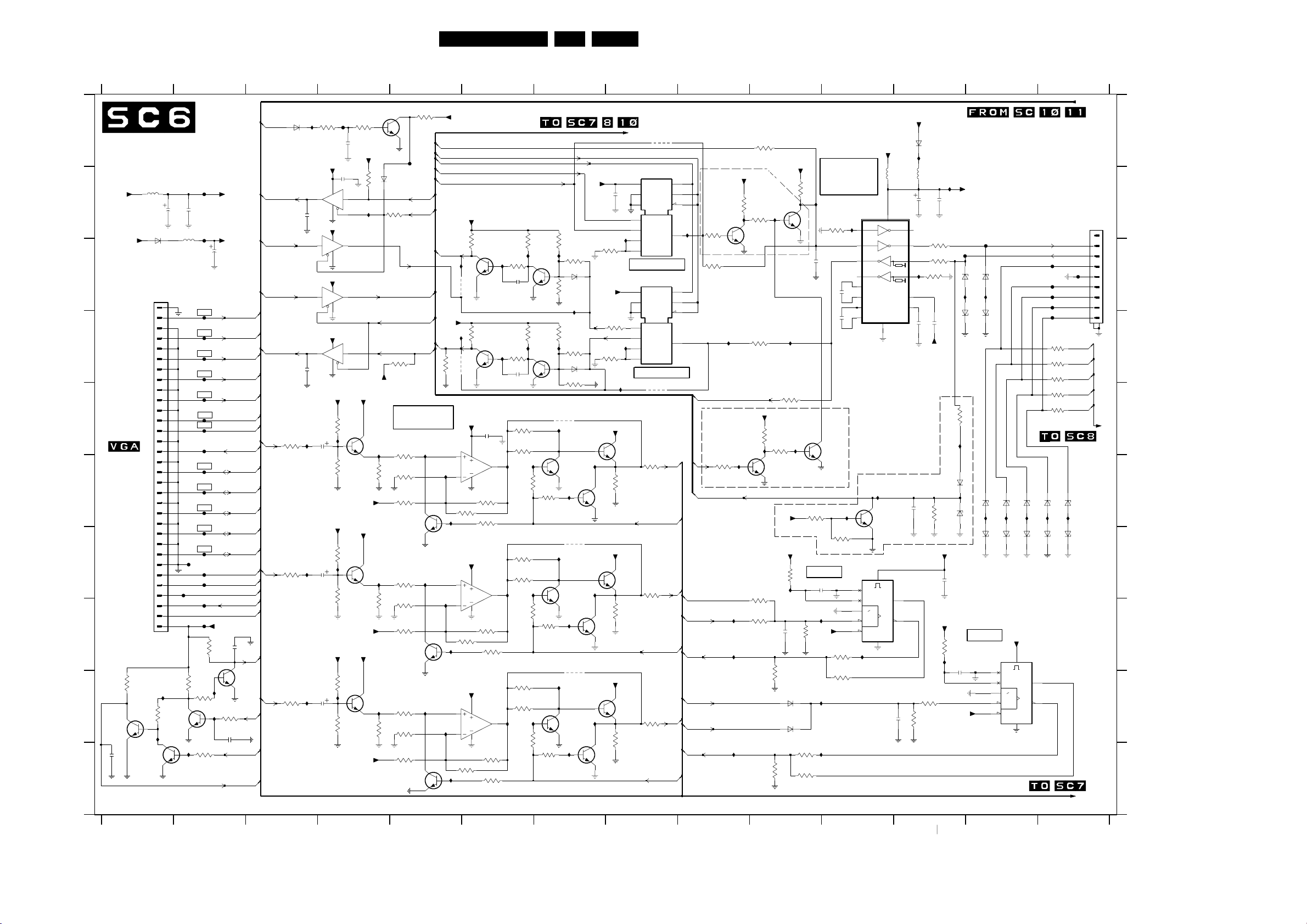
SCAVIO Panel: VGA Input
12345678
A
VGA INPUT
(BASIC AND ENHANCED VERSION)
+8V6
B
+5V_STBY_SW
100MHZ
C
D
E
TO
0318
F
G
H
4K7
3900
I
7320
BC847BW
2338
4V8
I289
RES
BC847BW
J
3122 123 6001.7
1
5300
2300
6302
BAT254
0318
VGA PANEL
CONNECTOR
I277
10K
3337
BC847BW
0V
7321
F300
100u
100n
2301
F301
5302
100MHZ
32
F303
31
30
F304
29
28
F305
27
26
F306
25
24
F307
23
22
F308
21
F309
20
19
F310
18
17
F311
16
15
F312
14
13
F313
12
11
F314
10
9
F315
8
F318
7
F316
6
F317
5
F324
4
F323
3
2
F319
1
3363
4K7
3305
3336
10K
0V
7322
0V6
0V
I290
10K
3339
0V6
Electrical Diagrams and PWB Layouts
10u
2302
+5V_STBY_SW
4K7
0V
I279
I284
33K
3338
2337
100p
+8B
+5S
VGA1_R
VGA1_G
VGA1_B
VGA1_H
VGA1_V
VGA1_TXD
VGA1_RXD
RC_VGA1
VGA2_R
VGA2_G
VGA2_B
VGA2_H
VGA2_V
VGA2_TXD
VGA2_RXD
TV_MODE
RC_OUT
VGA2_OUTN
2336
RC_OUT
4V8
7323
BC847BW
RC_CNTL
RC_VGA1
RES
7310
I220
6310
VGA1_RXD
BAT254
7303-B
74HCT125D
3308
270R
3318
270R
3328
270R
4V6
2305
4V3
4V5
4V5
2306
I244
I261
I280
VGA1_TXD
VGA1_RXD
VGA2_TXD
VGA2_RXD
VGA1_R
VGA1_G
VGA1_B
RC
2V0
0V1
F325
3910
1K
+5S
2304
100n
14
6
7
RES
+5S
14
2
7
1
+5S
14
12
7
13
+5S
74HCT125D
14
8
7
RES
+8B
3309
2308
2V3
22u
3905
+8B
3319
2318
2V2
22u
3906
+8B
3329
2328
2V3
22u
3907
3911
2310
100n
+5V_STBY_SW
5
3V7
0V1
4
7303-A
74HCT125D
3
4V6
7303-D
74HCT125D
11
7303-C
9
2V0
10
+8B
27K
I243
10K
+8B
27K
I260
10K
+8B
27K
I278
10K
BC847BW
0V6
47K
4K7
3917
6311
I224
+5V_STBY_SW
7308
BC847BW
I247
1V6
3310
+8B
7318
BC847BW
I262
1V6
3320
+8B
7328
BC847BW
I282
1V6
3330
+8B
1K
1K
1K
3912
0V
4K7
F326
BAT254
TXD_OTC
3908
SELECT_1
10K
TXD_2
SELECT_4
RXD_2
3923
4K7
VGA OUTPUT
BUFFERS
I248
3311
1K
3312
1K8
3313
10K
7309
BC847BW
I263
3321
1K
3322
1K8
3323
10K
7319
BC847BW
I283
3331
1K
3332
1K8
3333
10K
7333
BC847BW
TXD_2
SELECT_3
SELECT_2
TXD_OTC
TXD_PW
RXD_OTC
RXD_PW
I254
1V6
1V6
I268
I288
+5V
3372
1V6
I258
I272
1V6
I294
+5S
+3V3_STBY_SW
3307
3V2
I295
RES
4898
3317
I296
3V3
RES
10K
4316
+8B
5
6
3300
15K
+8B
10
9
1V6
3316
15K
+8B
12
13
1V6
3306
15K
4K7
7315
BC847BW
4K7
7325
BC847BW
2311
100n
7311-A
4
TSH93
11
3314
1K8
3297
10K
7311-B
4
TSH93
11
3324
1K8
3298
10K
7311-C
4
TSH93
11
3334
1K8
3299
10K
1V9
2V0
0V
0V
2V0
I232
I241
7
8
14
10K
3327
I230 I231
7316
BC847BW
3326
0V
1K
2341
RES
10K
3295
I239
7326
BC847BW
3294
0V
1K
2345
RES
3902
470R
3315
470R
I250
I253
10K
3356
3903
470R
3325
470R
I265
I267
10K
3301
3904
470R
3335
470R
I285
I287
10K
3367
3357
3302
3368
3348
0V7
3914
3296
I240
0V6
I242
10K
I259
10K
I276
10K
23456
470K
3349
33K
BAT254
6380
RES
I218
470K
3901
33K
6381
BAT254
3915
4315
7356
BC847BW
7357
BC847BW
I255
4325
7305
BC847BW
7306
BC847BW
I271
4335
7365
BC847BW
7366
BC847BW
I291
7
45FM242 AB 7.
9 1011121314
+5V_STBY_SW
RES
4011
7340-A
74HC4052D
+5R
3340
10K
2340
I228
3V3
2V7
100n
16
7
1
5
2
4
VCC
VEE
GND
0
1
2
3
MDX
10
0
9
1
68
G4
3
I229
4:1 SWITCH
7340-B
74HC4052D
16
+5R
RXD_O
3922
RXD_P
3346
10K
RES
I251
I266
I286
1K
I238
I219
+8B
7358
BC847BW
3358
+8B
7307
BC847BW
3303
+8B
7367
BC847BW
3369
VCC
7
VEE
8
GND
12
4V6
14
0V7
1
15
11
4:1 SWITCH
4K7
4K7
4K7
MDX
0
2
3
4008
RES
3359
68R
VGA2_OUTN
3304
68R
VGA2_OUTN
3351
68R
VGA2_OUTN
G4
VGA2_R
VGA2_G
VGA2_B
10
0
1
13
4V8
4V8
4V8
0V4
9
6
5V1
SELECT_4
RS_232_ACT
RXD_O
VGA1_RXD
UART_ACT
VGA1_H
VGA1_V
SYNC_ACT
RXD_2
RES
3341
33K
3913
100R
RES
7341
BC847BW
3360
10K
I269
I273
I292
I226
I252
+5R
3342
1K
I249
3343
33K
3350
100R
3920
RES
3371
100R
3345
RES
+5R
3361
7360
BC847BW
7343
BC847BW
I225
4K7
3362
10K
+5V
3373
MCL4148
3379
2335
2K2
2K2
I237I236
3347
100R
+5S
3370
I264
6378
6379
RES
I245
RES
+5R
3344
470K
9V9
3909
3378
RES
3918
1K
DOWN-
CONVERTER
4K7
I223
3352
10K
RES
2343
7362
BC847BW
3364
10K
1 SHOT
2370
100n
I270
10K
+5S
I281
I293
RS232
7352
ST3232E
10
TR2I
I227
TR1I
11 14
0V
REC1O
12
5V1
REC2O
9
1
C1+
3
100n
2351
C1-
4
C2+
5
C2-
2352
100n
RES
I257
0V7
3921
10K
RES
7370-B
74HCT4538
15
CX
RCX
12
11 9
4V3
13
R
I274
3374
RES
3919
1K
I256
0V
7364
BC847BW
>
1
GND
16
8
VCC
5352
15
+5V
100MHZ
16
TR2O
TR1O
REC1I
REC2I
2376
RES
6353
BAT254
I221
RES
5350
100MHZ
I222
+5R
10u
2353
7
13
8
I233
2
V+
6
V-
2355
2365
1014
0V
0V
RES
3376
9V9
0V
4K7
100n
3377
100R
100n
3355
10K
2356
+5R
3365
I275
2354
3353
100R
3354
100R
0V1
100n
+5S
2372
+5S
470K
3375
100n
6366
6365
100n
100K
2375
100n
3366
F320
6354
6356
1K
I246
F322
6355
BZM55-C33
BZM55-C33
I235
I234
6357
BZM55-C33
BZM55-C33
{RL_ICN,GL_ICN,LD_ICN,IR_TX,IR_RX}
MCL4148
6317
6315
BZM55-C6V8
6316
1 SHOT
7370-A
74HCT4538
3V3
+5S
6319
BZM55-C33
6318
CX
RCX
R
>
I298
6320
BZM55-C33
+5S
16
1
8
BZM55-C33
I299
BZM55-C33
BZM55-C33
I297
BZM55-C33
1
2
4
57
3
RS232 INPUT
OUTPUT
0376
1
2
3924
330R
3925
330R
3926
330R
3927
330R
3928
330R
6323
BZM55-C33
I300
6324
BZM55-C33
4V5
F321
RL_ICN
GL_ICN
LD_ICN
IR_TX
IR_RX
BZM55-C33
I301
BZM55-C33
3
4
5
6
7
8
9
10
140703
F327
F328
F329
F330
F331
6321
6322
6
4V5
CL 36532051_019.eps
11
0318 C1
0376 B14
2300 B1
2301 B2
2302 B2
2304 B4
2305 B3
2306 D3
A
2308 E4
2310 A4
2311 E6
2318 G4
2328 I4
2335 H10
2336 H2
2337 I2
2338 J1
2340 B8
2341 C6
2343 C10
B
2345 D6
2351 C11
2352 D11
2353 B12
2354 B12
2355 D12
2356 D12
2365 F12
2370 G10
2372 G12
2375 H12
2376 I12
C
3294 D6
3295 D6
3296 D7
3297 F6
3298 H6
3299 J6
3300 F6
3301 H6
3302 H7
3303 H8
3304 G8
3305 I2
D
3306 J6
3307 C6
3308 E3
3309 E4
3310 F4
3311 E5
3312 F5
3313 F5
3314 F6
3315 E6
3316 H6
E
3317 D6
3318 G3
3319 G4
3320 H4
3321 G5
3322 H5
3323 H5
3324 H6
3325 G6
3326 C6
3327 C6
3328 I3
F
3329 I4
3330 I4
3331 I5
3332 I5
3333 J5
3334 J6
3335 I6
3336 I2
3337 I1
3338 I2
3339 J2
3340 C8
G
3341 B9
3342 B9
3343 B10
3344 B10
3345 A10
3346 D8
3347 E10
3348 C7
3349 C7
3350 D10
3351 I8
H
3352 B11
3353 C12
3354 C12
3355 C12
3356 F6
3357 F7
3358 F8
3359 F8
3360 F9
3361 E10
3362 E10
3363 H2
I
3364 F10
3365 F12
3366 E12
3367 I6
3368 J7
3369 I8
3370 G10
3371 H10
3372 D5
3373 I10
3374 H11
J
3375 H12
3376 I12
3377 I12
3378 J10
3379 J10
3900 I1
3901 D7
3902 E6
3903 G6
3904 I6
3905 F4
3906 G4
3907 I4
3908 B5
3909 H10
3910 A4
3911 A4
3912 A5
3913 C9
3914 C7
3915 D7
3917 B4
3918 J10
3919 I11
3920 G10
3921 G11
3922 D8
3923 D5
3924 D14
3925 D14
3926 D14
3927 E14
3928 E14
4008 E8
4011 A8
4315 E7
4316 D5
4325 G7
4335 I7
4898 C5
5300 B1
5302 B2
5350 B12
5352 B11
6302 B1
6310 A3
6311 B4
6315 F13
6316 G13
6317 F13
6318 G13
6319 F13
6320 G13
6321 F14
6322 G14
6323 F14
6324 G14
6353 A12
6354 C12
6355 C13
6356 D12
6357 D13
6365 F12
6366 F12
6378 I10
6379 I10
6380 C7
6381 D7
7303-A B4
7303-B B4
7303-C D4
7303-D C4
7305 G7
7306 H7
7307 G8
7308 E4
7309 F5
7310 A4
7311-A E6
7311-B G6
7311-C I6
7315 C6
7316 C7
7318 G4
7319 H5
7320 I1
7321 J1
7322 I2
7323 I2
7325 D6
7326 D7
7328 I4
7333 J5
7340-A B8
7340-B C8
7341 B9
7343 B10
7352 B11
7356 F7
7357 F7
7358 E8
7360 F10
7362 E11
7364 F11
7365 I7
7366 I7
7367 I8
7370-A H13
7370-B G11
F300 B2
F301 B2
F303 D2
F304 D2
F305 D2
F306 D2
F307 E2
F308 E2
F309 E2
F310 E2
F311 F2
F312 F2
F313 F2
F314 G2
F315 G2
F316 G2
F317 G2
F318 G2
F319 H2
F320 C12
F321 C14
F322 C13
F323 H2
F324 G2
F325 A4
F326 B5
F327 C14
F328 C14
F329 C14
F330 C14
F331 D14
I218 C7
I219 E8
I220 A3
I221 A12
I222 B12
I223 B11
I224 B4
I225 B10
I226 B9
I227 B11
I228 B8
I229 C9
I230 C6
I231 C7
I232 C6
I233 C12
I234 C13
I235 C13
I236 D9
I237 D10
I238 D8
I239 D6
I240 D7
I241 D6
I242 E7
I243 E4
I244 E3
I245 E10
I246 E13
I247 E4
I248 E5
I249 E10
I250 F6
I251 F7
I252 F9
I253 F6
I254 F5
I255 F7
I256 F11
I257 F11
I258 F5
I259 G7
I260 G4
I261 G3
I262 G4
I263 G5
I264 G10
I265 G6
I266 G7
I267 G6
I268 H5
I269 H9
I270 H10
I271 H7
I272 H5
I273 H9
I274 H11
I275 H12
I276 I7
I277 I1
I278 I4
I279 I2
I280 I3
I281 I10
I282 I4
I283 I5
I284 I2
I285 I6
I286 I7
I287 I6
I288 I5
I289 I1
I290 J2
I291 J7
I292 J9
I293 J10
I294 J5
I295 C6
I296 D5
I297 F13
I298 F13
I299 F13
I300 F14
I301 F14
8 9 10 11 12 13 14
Page 46
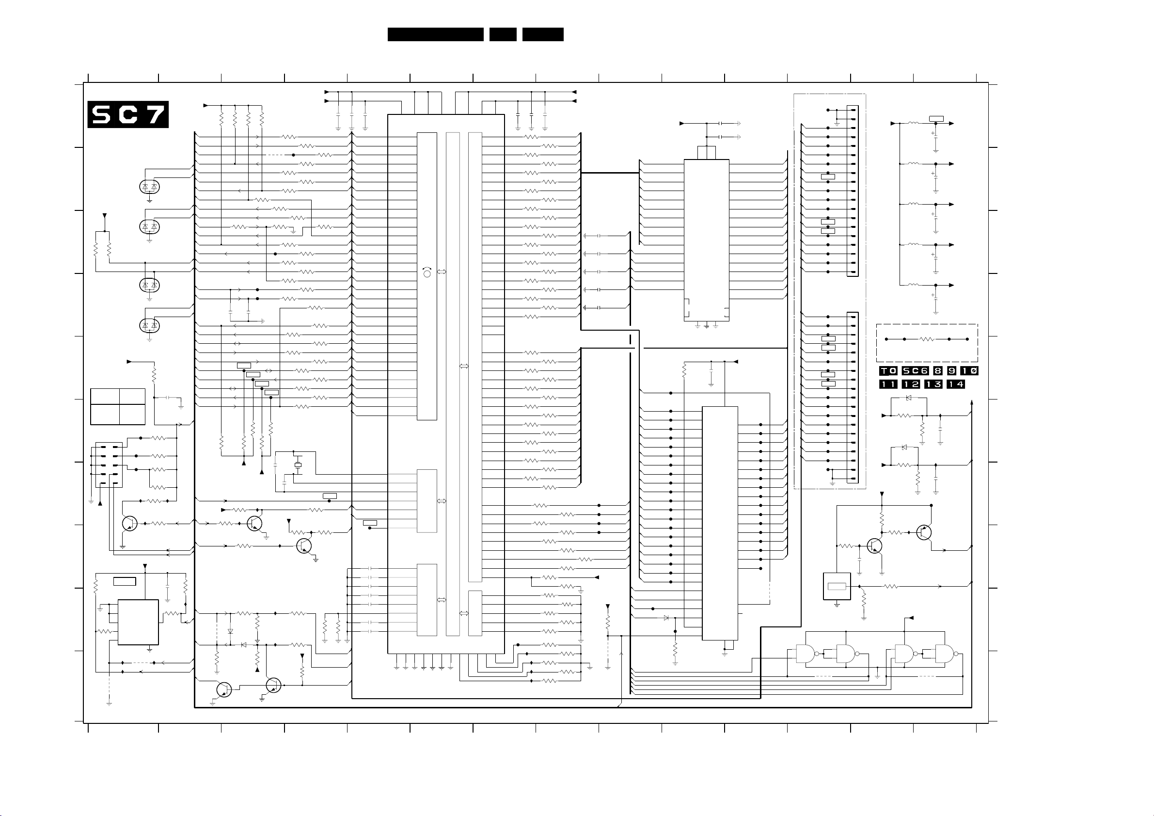
Electrical Diagrams and PWB Layouts
46FM242 AB 7.
SCAVIO Panel: Control Functions 1
1
23
CONTROL FUNCTIONS 1
+3V3_CNTL_D
A
(BASIC AND ENHANCED
VERSION)
B
C
3519
+3V3
2K2
3520
6821
PLVA2650A
6388
PLVA2650A
2K2
6393
PLVA2650A
D
6399
PLVA2650A
+3V3_CNTL_D
E
SERVICE SOCKET
SHORT
MODE
CIRCUIT
1 - 2
SDM
3 - 4
SAM
0382
147279
4K7
3431
100R
4430
5 - 6
F382
2
F380
F381
8
10
I352
3V2
7435
BC847BW
0V
I358
+3V3_CNTL_D
NVM
7430
MC24C32
1
E0
2
E1
3
E2
6
SCL
7
WC_
I364 I365
4431
I366
RES
COMPAIR
F
1
34
56
7
9
G
+5V
H
3430
I
J
3122 123 6001.7
12
VCC
8
VSS
LIGHT_SEN_IN
SERVICE_IN
1K
3418
2420
100n
SERVICE_IN
3419
3K9
3422
1K5
1K
3421
3420
2K2
I353
3417
RES
RS_232_ACT
3423
RES
5
SDA
4
SCL_NVM_1
RED_LED
FAN_SP_2
FAN_SP_1
IRQ_PDP
SCL_1
SDA_1
100n
2432
I363
3433
100R
SDA_NVM_1
RESET
RC
3432
4K7
BC847BW
1K
3388
3385
LIGHT_SEN_IN
SERVICE_IN
ICONN_NOT
STANDBY
5V_TEST
8V_TEST
CPU_GO
PW_FLASH_RESET
GRN_LEDGRN_LED
RED_LED
RC
RC_CNTL
PW_RESET
WP
FAN_SP_2
FAN_SP_1
UART_ACT
SYNC_ACT
2418
PW_START
SCL_NVM_1
SDA_NVM_1
TXD_OTC
RXD_OTC
SDA_2
SCL_2
SDA_1
SCL_1
IRQ_PDP
3K3
3411
+3V3_CNTL_D
RESET
+3V3_CNTL_C
VGA1_H
3427
RES
VGA1_V
POWER_OK
RES
4381
7406
3496
BAT254
10K
+3V3_CNTL_D
PDP_GO
CPU_GO
4567891011121314
+3V3_CNTL_B
+3V3_CNTL_A
3392
100R
3398-C
100R
3402-B
100R
3402-D
100R
3404-B
100R
3404-D
100R
6M
CX-5F
3428
100R
7433
BC847BW
3K3
3381-D
100R
3382-C
100R
3429
100R
3435
0V
0V
F423
2381
P2_2
P2_3
P3_7
P3_6
P3_5
P3_4
P3_3
P3_1
P3_0
P2_7
P2_6
P2_5
P2_4
P2_1
P2_0
P1_7
P1_6
P1_5
P1_4
P1_2
P0_7
P0_6
P0_5
P0_4
P0_3
P0_2
P0_1
P0_0
P1_0
OTC_H
OTC_V
27K
3436
P1_3
P3_2
P1_1
1K
RES
3009
3390
1K
F525
F526
1n
1n
2419
F425
F426
3413
2K2
3410
+5V_STBY_SW
I354
3424
3K3
I357
3425
RES
3393
1K
3394
6508
BAT254
6509
3387
3386
3018
100R
F427
2K2
3414
7432
BC847BW
2K2
1K
RES
F428
3380-B
100R
F430
4385
RES
3381-B
100R
3382-D
100R
3382-B
100R
3391
33K
3384
F431
100R
3380-A
100R
3383-C
100R
3383-A
100R
3402-A
100R
3402-C
100R
4K7
3415
4K7
33p
2415
2416
+3V3_CNTL_C
I360
I345
I344
+3V3_CNTL_D
7405
BC847BW
3382-A
100R
3404-A
100R
3404-C
100R
3397
RES
1415
27p
3426
3K3
3398-A
100R
3389
100R
3380-C
100R
3381-C
100R
3381-A
100R
3401
RES
3383-D
100R
3383-B
100R
I355
3405
34
100n
220K
7383
100n
2382
P2_2
P2_3
P3_7
P3_6
P3_5
P3_4
P3_3
P3_2
P3_1
P3_0
P2_7
P2_6
P2_5
P2_4
P2_1
P2_0
P1_7
P1_6
P1_5
P1_4
P1_3
P1_2
P0_7
P0_6
P0_5
P0_4
P0_3
P0_2
P0_1
P0_0
P1_0
P1_1
OTC_H
OTC_V
2433
2434
2435
2436 100n
2437
2438
2439
2383
F383
100n
3V2
0V
3V4
3V4
3V2
3V2
1V2
3V1
3V2
3V1
3V1
3V1
100n
100n
100n
SAA5801H
105 P2-2|ADC0
106 P2-3|ADC1
120 P3-7|CBB
119 P3-6|TTC
0V
118 P3-5|TTD
117 P3-4
116 P3-3
115 P3-2
114 P3-1|LED1
113 P3-0|LED0
110 P2-7|ADC5
109 P2-6|ADC4
0V
108
107 P2-4|ADC2
104 P2-1|PWM1
0V
103 P2-0|PWM0
0V
100 P1-7|RC
99 P1-6|INT3
0V
98 P1-5|INT2
97 P1-4|INT1
96 P1-3|INT0
2V
95 P1-2|T2
92
2V
90 P0-5|TxDo
89 P0-4|RxDo
88 P0-3|SDA1
87 P0-2|SCL1
86 P0-1|SDA0
85 P0-0|SCL0
93 P1-0|T0
94 P1-1|T1
16 OSCOUT
17 OSCIN
18 OSCGND
74 RESET
83 HSYNC
84 VSYNC
82 FRAME
5 CVBS0
4 CVBS0_R
7 CVBS1
6 CVBS1_R
100n
1 IREF_DEC
2 IREF
220n
3
220n
8 STN|BLACK
P2-5|ADC3
P0-7
P0-6|CORN91
REF+
VSSA21VSSD176VSSD2
10
9
VDDA
20
VDD1
VDDN1
AND
DISPLAY TIMING
CLOCK GENERATOR
TXT
CAPTION
EPG
USA
CLOSE
TXT
VSSP150VSSP2
56
111
75
38
VDDP149VDDP2
EXTERNAL CODE AND DATA INTERFACE
VSSD3
VSSP3
10239
112
10119
VDDD2
VDDD3
DISPLAY
INTERFACE
TEST0
TEST113TEST214TEST315TEST4
11 12
A10
FADING
VIDEOn
VDDP3
A1
A4
45
47A2
51A3
53
55A5
57A6
59A7
61A8
62A9
60
58A11
56A12
54A13
52A14
48A15
46A16
44A17
63A18
65A19
64A20
66A21
67A22
68A23
36D0
32D1
28D2
24D3
23D4
27D5
31D6
35D7
34D8
30D9
26D10
22D11
25D12
29D13
33D14
37D15
40ROM_OEn
41RAM_OEn
43ROM_CSn
42PSENn
69RASn
72CASLn
71CASHn
70WEn
73EAn
77R
78G
79B
80
81DATA
7 8 9 1011121314
2446
F490
100n
3448-A
100R
3449-A
100R
3451-A
100R
3452-A
100R
3452-D
100R
3451-D
100R
3449-D
100R
3448-D
100R
3450
100R
3453-C
100R
3453-D
100R
3463-C
100R
3461-C
100R
3460-B
100R
3462-B
100R
3463-A
100R
3461-A
100R
3460-D
100R
3462-D
100R
I346
I347
I348
2447
I349
100n
3464-A
100R
3464-D
100R
2448
3448-C
100R
3449-C
100R
3451-C
100R
3452-C
100R
3452-B
100R
3451-B
100R
3449-B
100R
3448-B
100R
3453-A
100R
3453-B
100R
3462-C
100R
3460-C
100R
3461-B
100R
3463-B
100R
3462-A
100R
3460-A
100R
3461-D
100R
3463-D
100R
3406-A
100R
3483
470R
3485
150R
3487
150R
3489
2K2
3490
1K
3494-C
470R
3494-A
470R
100n
+3V3_CNTL_C
+3V3_CNTL_D
AC(0)
AC(1)
AC(2)
AC(3)
AC(4)
AC(5)
AC(6)
AC(7)
AC(8)
AC(9)
AC(10)
AC(11)
AC(12)
AC(13)
AC(14)
AC(15)
AC(16)
AC(17)
AC(18)
AC(19)
AC(20)
DC(0:15)
DC(0)
DC(1)
DC(2)
DC(3)
DC(4)
DC(5)
DC(6)
DC(7)
DC(8)
DC(9)
DC(10)
DC(11)
DC(12)
DC(13)
DC(14)
DC(15)
3464-B
100R
3464-C
63
100R
3406-D
100R
3406-C
100R
3406-B
100R
3484
RES
3486
150R
3488
2K2
3494-D
470R
3494-B
470R
+3V3_CNTL_E
MSM51V18165F
17
18
19
20
23
24
25
26
27
28
14
31
30
13
29
11
12
15
F459
F460
F461
F462
F463
F464
F465
F466
F467
F468
F469
F470
F471
F472
F473
F474
F475
F476
F477
F478
F479
6507
BAT254
F507
3507
7500
NC
3506
4K7
AC(0:20)
AC(0)
AC(1)
AC(2)
AC(3)
AC(4)
AC(5)
AC(6)
WE
RAS
RAS
WE
RES
RAS
CASL
CASH
WE
RAM_OE
DC(0:15)
AC(0:20)
AC(0:20)
CS
OE
WE
RESET_FLASH
WP
RAM_CS
ROM_CS
CS
ROM_OE
RAM_OE
OE
AC(7)
AC(8)
AC(9)
AC(20)
AC(0)
AC(1)
AC(2)
AC(3)
AC(4)
AC(5)
AC(6)
AC(7)
AC(8)
AC(9)
AC(10)
AC(11)
AC(12)
AC(13)
AC(14)
AC(15)
AC(16)
AC(17)
AC(18)
AC(19)
F506
2504
82p
2501
82p
2502
CASH
82p
2503
RAM_OE
82p
2505
CASL
82p
F421
ROM_OE
F420
RAM_OE
F422
ROM_CS
F424 F483
RAM_CS
CASL
CASH
+3V3_CNTL_C
+3V3_CNTL_E
3503
3502
A0
VCC11VCC26VCC3
A1
A2
A3
A4
A5
A6
RAM
A7
A8
A9
RAS_
LCAS_
UCAS_
WE_
OE_
VSS122VSS237VSS3
3K3
7506
AM29DL164DT
25
A0
24
A1
23
A2
22
A3
21
A4
20
A5
19
A6
18
A7
8
A8
7
A9
6
A10
5
A11
4
A12
3
A13
2
A14
1
A15
48
A16
17
A17
16
A18
9
A19
26
CE_
28
OE_
11
WE_
12
RESET_
47
BYTE_
14
WP_|ACC
2506
2500
100n
2499
100n
21
2
DQ1
3
DQ2
4
DQ3
5
DQ4
7
DQ5
8
DQ6
9
DQ7
10
DQ8
33
DQ9
34
DQ10
35
DQ11
36
DQ12
38
DQ13
39
DQ14
40
DQ15
41
DQ16
16
NC
32
42
100n
37
VCC
DQ0
DQ1
DQ2
DQ3
DQ4
DQ5
DQ6
DQ7
DQ8
DQ9
DQ10
DQ11
FLASH
DQ12
DQ13
DQ14
DQ15|A-1
RY|BY_
VSS
27 46
+3V3_CNTL_E
29
31
33
35
38
40
42
44
30
32
34
36
39
41
43
45
15
10
13
NC
F497
F496
F495
F494
F493
F492
F489
F488
F487
F486
F485
F484
F482
F481
F480
F432
DC(0)
DC(1)
DC(2)
DC(3)
DC(4)
DC(5)
DC(6)
DC(7)
DC(8)
DC(9)
DC(10)
DC(11)
DC(12)
DC(13)
DC(14)
DC(15)
DC(0)
DC(1)
DC(2)
DC(3)
DC(4)
DC(5)
DC(6)
DC(7)
DC(8)
DC(9)
DC(10)
DC(11)
DC(12)
DC(13)
DC(14)
DC(15)
4500
RES
74LVC00AD
P1_7
P2_0
P2_1
P2_2
P2_3
P2_4
P2_5
P2_6
P2_7
P3_0
P3_1
P3_2
P3_3
P3_4
P3_5
P3_6
P3_7
DEBUG
CONNECTORS
P1_6
P1_5
P1_4
P1_3
P1_2
P1_1
P1_0
P0_7
P0_6
P0_5
P0_4
P0_3
P0_2
P0_1
P0_0
OTC_V
OTC_H
7517
ADM810
7510-A
14
1
2
7
F384
F385
F386
F387
F388
F389
F390
F391
F392
F393
F394
F395
F396
F397
F398
F399
F400
F401
F402
F403
F404
F405
F406
F407
F408
F409
F410
F411
F412
F413
F414
F415
F416
F417
F418
F419
VCC
RESET
GND
7510-B
74LVC00AD
4
3
5
4505
3452-D B7
0382 F1
3453-A D8
0383 A12
3453-B D8
0384 D12
3453-C D7
1415 G4
3453-D D7
2381 A4
3460-A F8
S83
0383
1
2
+3V3_STBY_SW
3
4
5
6
7
8
9
10
11
12
13
14
15
16
17
18
19
S84
0384
1
2
3
4
5
6
7
8
9
10
11
12
13
14
15
16
17
18
19
3515
47K
3
1
+5V
+8V6
+3V3_CNTL_C
3514
I359
I361
0V6
2515
100n
I362
0V
2
3518
100K
14
7
74LVC00AD
6
F450
For Diversity
RES
BZX384-C2V4
RES
BZX384-C2V4
4K7
3516
0V
47K
7515
BC847BW
3517
1K
7510-C
9
10
100MHZ
100MHZ
100MHZ
100MHZ
100MHZ
F451
6504
3510
1K
6505
3512
5K6
I356
2V6
14
7
5520
5521
5522
5523
5524
3400
3511
3K3
3513
3V2
+3V3_CNTL_B
74LVC00AD
8
4506
F520
+3V3_CNTL_A
10u
2520
F521
+3V3_CNTL_B
10u
2521
F522
+3V3_CNTL_C
10u
2522
F523
+3V3_CNTL_D
10u
2523
F524
+3V3_CNTL_E
10u
2524
F453
F452
*
1K
Basic = 1K
*
Enhanced = 4K7
I350
5V_TEST
2K2
2511
100n
I351
8V_TEST
2513
100n
F429
7516
BC857BW
RESET_FLASH
RESET
7510-D
14
12
11
13
7
CL 36532051_020.eps
140703
2382 A5
3460-B E7
2383 A5
3460-C E8
2415 G3
3460-D F7
2416 G3
2418 D3
2419 D3
2420 E2
2432 H2
2433 H5
2434 H5
2435 H5
2436 I5
2437 I5
2438 I5
2439 I5
2446 A7
2447 A7
2448 A8
2499 A10
2500 A10
2501 C8
2502 C8
2503 D8
2504 C8
2505 D8
2506 E10
2511 F14
2513 G14
2515 H13
2520 A14
2521 B14
2522 C14
2523 C14
2524 D14
3009 A3
3018 B3
3380-A C4
3380-B A4
3380-C A4
3381-A B4
3381-B B4
3381-C B4
3381-D B4
3382-A C4
3382-B B3
3382-C C4
3382-D B4
3383-A D4
3383-B D4
3383-C D4
3383-D C4
3384 C4
3385 A3
3386 A3
3387 J3
3388 A2
3389 I4
3390 C3
3391 C3
3392 D4
3393 I3
3394 I3
3397 F4
3398-A I4
3398-C D4
3400 D14
3401 C4
3402-A D4
3402-B E4
3402-C E4
3402-D E4
3404-A E4
3404-B E4
3404-C E4
3404-D E4
3405 J4
3406-A H8
3406-B H8
3406-C H8
3406-D H8
3410 F3
3411 F2
3413 F3
3414 F3
3415 F3
3417 G1
3418 E1
3419 F2
3420 G2
3421 G1
3422 F2
3423 G1
3424 G3
3425 H3
3426 H4
3427 G3
3428 G4
3429 H4
3430 H1
3431 I1
3432 H2
3433 I2
3435 I4
3436 I4
3448-A A7
3448-B C8
3448-C A8
3448-D C7
3449-A B7
3449-B C8
3449-C B8
3449-D C7
3450 D7
3451-A B7
3451-B C8
3451-C B8
3451-D C7
3452-A B7
3452-B C8
3452-C B8
3461-A F7
3461-B E8
3461-C E7
3461-D G8
3462-A F8
3462-B F7
3462-C E8
3462-D G7
3463-A F7
3463-B F8
3463-C E7
3463-D G8
3464-A G8
3464-B G8
3464-C H8
3464-D G8
3483 H8
3484 H8
3485 I8
3486 I8
3487 I8
3488 I8
3489 I8
3490 I8
3494-A J8
3494-B J8
3494-C J8
3494-D I8
3496 J2
3502 I9
3503 I9
3506 E10
3507 I10
3510 F13
3511 F14
3512 F13
3513 G14
3514 G13
3515 H12
3516 H13
3517 H13
3518 I13
3519 C1
3520 C1
4381 I2
4385 B3
4430 J1
4431 J1
4500 I11
4505 J12
4506 J14
5520 A13
5521 B13
5522 B13
5523 C13
5524 D13
6388 C1
6393 D1
6399 D1
6504 E13
6505 F13
6507 I10
6508 I3
6509 J3
6821 B1
7383 A5
7405 J3
7406 J2
7430 I1
7432 G3
7433 H4
7435 G1
7500 B10
7506 F10
7510-A I12
7510-B I12
7510-C I13
7510-D I14
7515 H13
7516 H14
7517 H12
F380 F1
F381 G1
F382 F1
F383 G5
F384 A12
F385 A12
F386 A12
F387 A12
F388 B12
F389 B12
F390 B12
F391 B12
F392 B12
F393 B12
F394 B12
F395 C12
F396 C12
F397 C12
F398 C12
F399 C12
F400 C12
F401 C12
F402 D12
F403 D12
F404 D12
F405 E12
F406 E12
F407 E12
F408 E12
F409 E12
F410 E12
F411 E12
F412 F12
F413 F12
F414 F12
A
B
C
D
E
F
G
H
I
J
F415 F12
F416 F12
F417 F12
F418 F12
F419 G12
F420 G9
F421 G9
F422 G9
F423 G4
F424 H9
F425 E3
F426 E3
F427 E3
F428 E3
F429 G14
F430 B4
F431 C3
F432 H11
F450 D13
F451 D13
F452 D14
F453 D14
F459 E10
F460 F10
F461 F10
F462 F10
F463 F10
F464 F10
F465 F10
F466 F10
F467 G10
F468 G10
F469 G10
F470 G10
F471 G10
F472 G10
F473 G10
F474 H10
F475 H10
F476 H10
F477 H10
F478 H10
F479 H10
F480 H11
F481 H11
F482 H11
F483 H11
F484 G11
F485 G11
F486 G11
F487 G11
F488 G11
F489 G11
F490 I7
F492 G11
F493 F11
F494 F11
F495 F11
F496 F11
F497 F11
F506 I9
F507 I10
F520 A14
F521 B14
F522 B14
F523 C14
F524 D14
F525 D3
F526 D3
I344 I3
I345 I3
I346 I7
I347 J7
I348 J7
I349 J7
I350 F14
I351 F14
I352 G1
I353 G2
I354 G3
I355 H4
I356 H13
I357 H3
I358 H1
I359 H13
I360 H3
I361 H13
I362 H13
I363 I2
I364 J1
I365 J1
I366 J1
Page 47
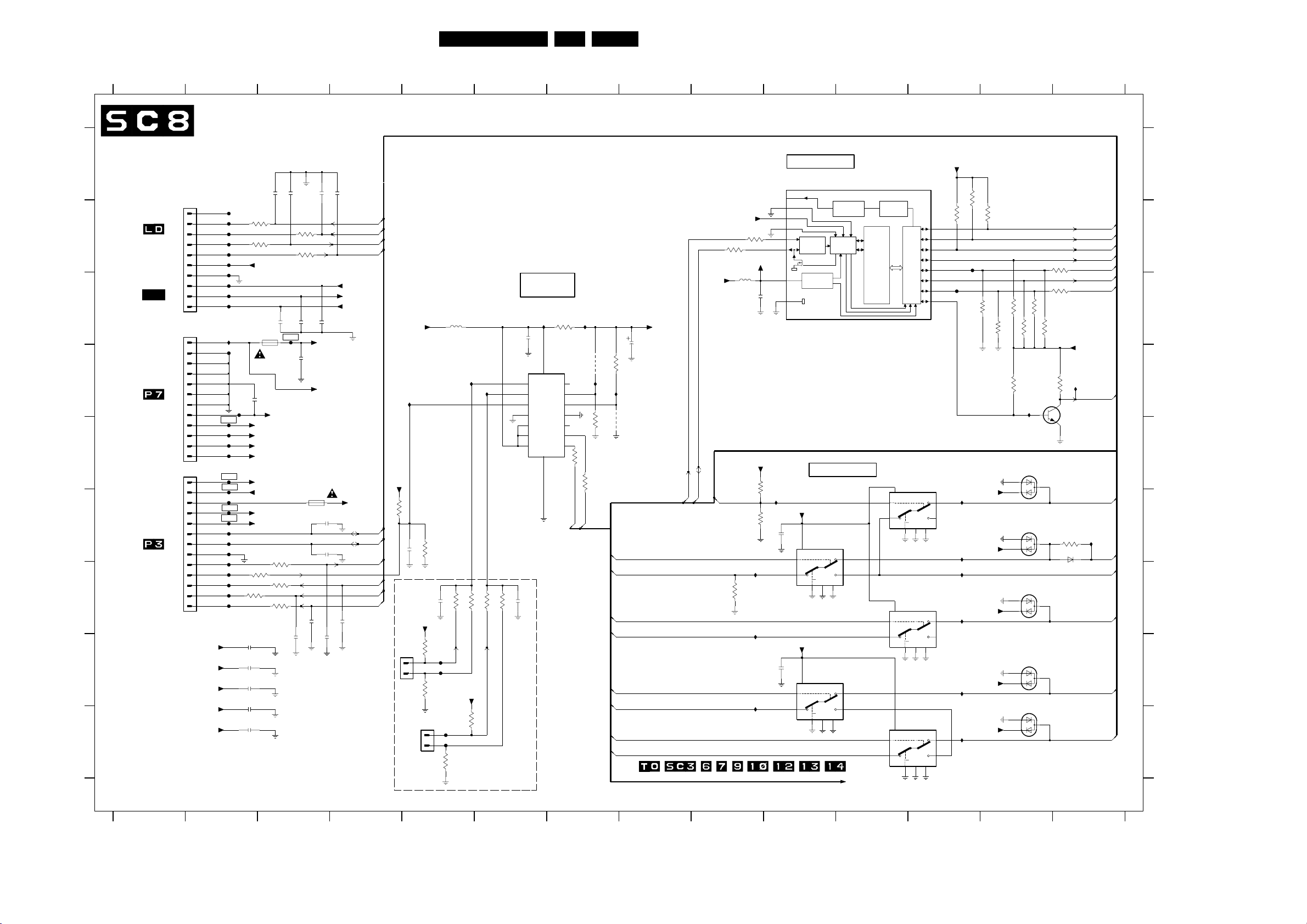
Electrical Diagrams and PWB Layouts
SCAVIO Panel: Control Functions 2
1234567
CONTROL FUNCTIONS 2
(BASIC AND ENHANCED VERSION)
A
B
LED-PANEL
DISPLAY
C
EMC FILTER
PANEL
D
POWER
SUPPLY
E
F
POWER
SUPPLY
G
H
I
3122 123 6001.7
TO
0320
OR
1330
EMC
TO
0305
TO
0319
123
0320
1
0V3
2
3V2
3
3V3
4
5
6
7
8
9
10
0305
1
2
3
4
5
6
7
8
9
10
11
12
0319
1
2
3
4
5
6
7
8
9
3V1
10
11
12
13
+9V_STBY
+9V_STBY_SW
+8V6
+5V_STBY_SW
+3V3_STBY_SW
0V2
F530
F531
3550
F532
100R
F533
3552
F534
100R
F535
F536
F537
F538
F539
F545
F541
F542
F543
F544
F546
F547
F548
F549
F550
F551
F552
F562
F554
F555
F556
F557
0V
F553
0V
I400
F529
+8V6
2537
+3V3
+3V3
+3V3
+3V3
+9V_STBY
+9V_STBY_SW
+5V_STBY_SW
+3V3_STBY_SW
3545
220R
3559
100R
2562
1n
2563
1n
2564
1n
2565
1n
2566
1n
1100
T 1A
1n
47FM242 AB 7.
F549 F2
F550 F2
F551 F2
F552 F2
F553 G2
F554 F2
F555 G2
F556 G2
F557 G2
F558 H5
F559 H5
F560 I5
F561 I5
F562 F2
I400 C2
I401 C6
I402 C7
I403 D7
I404 F14
I405 D5
I406 D6
I407 D5
I408 D14
I409 D13
I410 F10
I411 G9
I412 G9
I413 H9
I414 I12
I415 D8
I416 H12
I417 G12
I418 G12
I419 F12
I420 F12
A
B
C
D
E
F
G
H
I
0305 C2
0315 H5
0316 I5
0319 E2
0320 B2
1100 C3
1105 F3
2530 C8
2531 C6
2533 G5
2534 G6
2535 F5
2537 D2
2538 D3
2541 C9
2543 F3
2544 F3
2546 C3
2547 C3
2548 C3
2550 A3
2551 A3
2552 A3
2553 A4
2554 H10
2555 F10
2557 H4
2558 G4
2559 H3
2560 G3
2562 H2
2563 H2
2564 H2
2565 H2
2566 I2
3530 C7
3531 E7
3532 E7
3533 G5
3534 G6
3535 F5
3536 F4
3537 H5
3538 I5
3539 H5
3540 B9
3541 B9
3542 B12
3543 A12
3544 B13
3545 G3
3546 C13
3547 C13
3548 D14
3549 I5
3550 B3
3551 B3
3552 B3
3553 B3
3554 G5
3555 G6
3556 E9
3557 G3
3558 G3
3559 G2
3560 G3
3561 C12
3562 D13
3563 C13
3564 B14
3565 C14
3566 C13
3567 C13
3568 D7
3569 E7
3570 F9
3572 E7
3573 D7
3577 G9
3578 F14
5530 C5
5541 C9
6551 H13
6552 H13
6553 G13
6554 F13
6555 E13
6556 F14
7530 D6
7540 A10
7550-A I12
7550-B H10
7555-A F10
7555-B E12
7555-C G12
7563 D14
F527 C12
F528 B12
F529 D2
F530 B2
F531 B2
F532 B2
F533 B2
F534 B2
F535 B2
F536 B2
F537 C2
F538 C2
F539 C2
F540 C3
F541 E2
F542 E2
F543 E2
F544 E2
F545 D2
F546 E2
F547 E2
F548 F2
8 9 10 11 12
I/O EXPANDER
7540
PCF8574AT
1n
1n
2550
2552
3551
100R
3553
100R
1n
1n
2547
2546
F540
L 63V
446
+3V3
2538
1n
1n
2551
1n
2548
+5V
+5V_POW
1n
2553
GREEN_LED
LIGHT_SEN_IN
+5V_STBY_SW
+9V_STBY_SW
+9V_STBY
RED_LED
RC_IN
I407
+5V
5530
100MHZ
I405
I406
7530
PCF8591
1
2
3
4
5
6
7
EXTERNAL
ADC
I401
AIN0
AIN1
AIN2
AIN3
A0
A1
A2
100n
VDD
VSS
100R
16
AOUT
VREF
AGND
EXT
OSC
SCL
SDA
8
2531
3530
+5V_EXP
3541
100R
+5V_STBY_SW
I402
3568
I403
15
14
13
12
11
10
9
3532
100R
3569
RES
3573
3572
+5VREF
22u
2530
RES
I415
5541
100MHZ
N.C.
3540
100R
+5V_EXP
2541
100n
+5V_STBY_SW
13
INT_
1
A0
2
A1
3
A2
14
SCL
15
SDA
16
VDD
8
VSS
INPUT
FILTER
POWER-ON
RESET
INTERRUPT
LOGIC
I2C BUS
CONTROL
SHIFT
REGISTER
LP FILTER
8 BIT
I/O
PORTS
P0 4
P1 5
P2 6
P3 7
P4 9
P5 10
P6 11
P7 12
ICONN SWITCH
7555-B
74HC4053D
16
Vdd
S
10
Z
15
E
Vee8Vss
6
7
7555-C
74HC4053D
16
Vdd
S
9
Z
4
E
Vee7Vss
6
7550-A
74HC4053D
16
Vdd
S
11
Z
14
E
Vee8Vss
7
6
3557
100R
3558
100R
3560
100R
2559
1105
F 500mA
RES
RES
2560
1n
1n
2543
2544
1n
1n
1n
L 32V
1n
2557
+8V6
SCL_1
SDA_1
POWER_OK
STANDBY
FAN_SP_1
FAN_SP_2
2558
+5VREF
3536
0315
TO
S - 1
TO
S - 2
RES
2K2
2535
3535
100n
+5VREF
3537
1
2
3539
0316
10K
10K
RES
2533
F558
F559
1
2
F560
F561
3549
3533
100n
TEMP_1
10K
10K
3554
+5VREF
3538
10K
3534
TEMP_2
10K
10K
3555
10K
2534
100n
3531
SDA_SW
SCL_SW
100R
ICONN_NOT
GRN_LED
ICONN_NOT
RED_LED
ICONN_NOT
RC
ICONN_NOT
RC_IN
SCL_1
SDA_1
3577
10K
RES
2K2
3556
I410
+5V_STBY_SW
3K3
3570
100n
2555
I411
I412
2554
I413
16
Vdd
S
11
Z
14
+5V_STBY_SW
100n
16
Vdd
S
10
Z
15
7555-A
74HC4053D
E
Vee7Vss
6
7550-B
74HC4053D
E
Vee7Vss
6
Y0
12
Y1
13
8
Y0
2
Y1
1
8
+5V_EXP
3543
RES
3542
0V
4V8
4V8
2V
F528
0V
3V2
F527
0V
0V
MSP_RESET_NOT
+5V_STBY_SW
I420
Y0
2
Y1
1
+5V_STBY_SW
I419
I418
+5V_STBY_SW
I417
Y0
5
Y1
3
8
+5V_STBY_SW
I416
+5V_STBY_SW
I414
Y0
12
Y1
13
13 14
RES
RES
3544
1K0
3563
RES
3546
1K0
3547
10K
3562
6555
BAV99W
1
2
6554
BAV99W
1
2
6553
BAV99W
1
2
6552
BAV99W
1
2
6551
BAV99W
1
2
3561
I409
3566
1K
RES
3567
3
3
3
3
3
3564
RES
3565
RES
RES
3548
1K
7563
BC847BW
3578
150R
6556
BAT254
RES
SELECT_1
SELECT_2
SELECT_3
SELECT_4
VIDEO_SEL_1
POWER_DOWN
VIDEO_SEL_2
+5V_EXP
I408
MSP_RESET
LD_ICNICONN_NOT
I404
GL_ICN
GREEN_LED
RL_ICN
IR_TX
IR_RX
CL 36532051_021.eps
140703
4567891011121314
Page 48
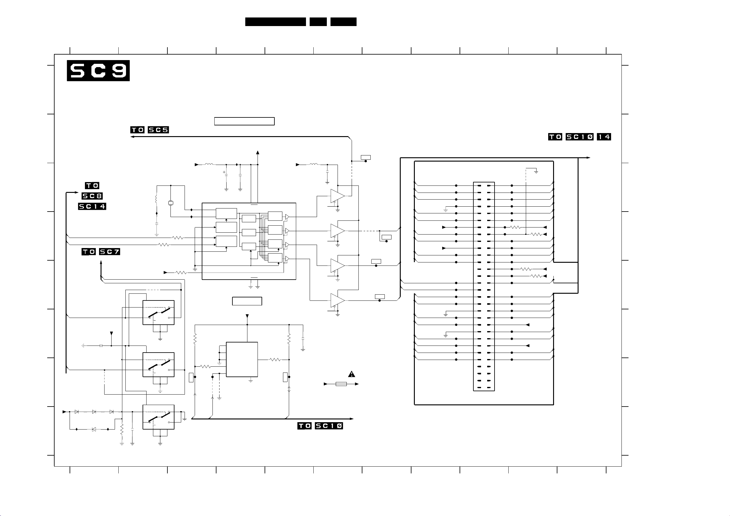
Electrical Diagrams and PWB Layouts
SCAVIO Panel: Scaler Clock Generator
12345
SCALER-CLOCK-GENERATOR
(BASIC AND ENHANCED VERSION)
A
4K7
2581
{VIDCLK}
9
4
10
15
11
14
100n
S
Z
S
Z
S
Z
Vdd
Vdd
Vdd
16
16
16
I433
+5V_0E
4593
5570
2570
RES
74HCT4053D
E
Vee8Vss
6
7571-B
74HCT4053D
Vee8Vss
E
6
7571-A
74HCT4053D
E
Vee8Vss
6
B
C
D
SCL_SW
SDA_SW
E
SCL_SW
F
SDA_SW
G
6500 6502
+5V
H
BZX384-C2V4
3122 123 6001.7
6501
6503
2584
100n
SDA_1
SCL_1
4592
I436I435
RES
RESRESRES
+5V_STBY_SW
3594
10u
1n
3571
100R
7
7
7
1570
7571-C
Y0
Y1
Y0
Y1
Y0
Y1
CX-11F
3016
100R
3575
5
3
2
1
12
13
24M576
1K
+5V
I430
I431
16 SCL
5V
3580
F567
PW_SCL_NVM
CLOCK GENERATOR
5572
100MHZ
10u
2573
7570
FS6377
5 XIN
6 XOUT
3PD
1 SDA
9 ADDR
2 SEL_CD
7OE
4K7
3581
100R
PWR DWN
F568
4582
4581
PW_RESET
REF
OSC
CTRL
2
I C BUS
INTERF
7580
M24C32
1
E0
2
E1
3
E2
6
SCL
7
WC_
0V4
RES
I432
100n
2572
PLL A
PLL B
PLL C
PW-NVM
+3V3_PW
8
VCC
SDA
VSS
+5V_0E
814
VDD
VSS
411
5
4
+3V3_STBY_SW
MUX A
MUX B
MUX C
MUX D
3583
3582
100R
F569
PW_SDA_NVM
4K7
15
13
12
10
2583
5574
100MHZ
7574-A
74LVC125A
74LVC125A
74LVC125A
74LVC125A
100n
+3V3
48FM242 AB 7.
6789
VIDCLK
24.576MHz
F566
2574
2
7574-B
5
7574-C
9
7574-D
12
1
4
10
13
100n
14
7
14
7
14
7
14
7
1575
F 500mA
441
3
6
8
11
L 32V
4572
4574
+3V3_PW
VXCA_18M432
F563
F564
F565
120MHz
DCKEXT
36MHz
MCLK
BOOTWE
ROMOE
A(2)
A(4)
A(6)
A(9)
A(11)
A(12)
A(14)
A(17)
A(19)
D(15)
D(14)
D(5)
D(4)
D(3)
D(2)
D(9)
D(8)
+3V3
+3V3
F570
F571
F572
F573
F574
F576
F577
F578
F579
F580
F581
F582
F583
F584
F585
F586
F587
F588
F589
F590
S86
0386
FTR
1
3
5
78
9
11 12
13
15 16
17 18
19
21 22
23 24
25 26
27 28
29
31 32
33 34
35 36
37 38
39
41 42
43 44
45 46
47 48
49
51 52
53 54
55 56
57 58
59
DEBUG CONNECTOR
2
4
6
10
F597
14
F598
20
30
40
50
60
PW
F591
F592
F593
F594
F595
F596F575
F599
F600
F601
F602
F603
F604
F605
F606
F607
F608
F609
F610
F611
F612
F613
10 11
RES
4591
A(1)
A(3)
A(5)
A(7)
A(8)
A(10)
3591
3K3
3593
3K3
+3V3
+3V3
+3V3
+3V3
A(13)
A(15)
A(16)
A(18)
+3V3
+3V3
ROMWE
D(7)
D(6)
D(13)
D(12)
D(11)
D(10)
D(1)
D(0)
3590
3K3
3592
3K3
A(0:19)
{ROMWE}
D(0:15)
CL 36532051_022.eps
140703
A
B
C
D
E
F
G
H
0386 C9
1570 C2
1575 G6
2570 D2
2572 C4
2573 C4
2574 C6
2581 H2
2583 F5
2584 F1
3016 D3
3571 D2
3575 E3
3580 F3
3581 G3
3582 F5
3583 F5
3590 D10
3591 D10
3592 E10
3593 E10
3594 H2
4572 C6
4574 D7
4581 G3
4582 G4
4591 C10
4592 G1
4593 E2
5570 C2
5572 B3
5574 B5
6500 G1
6501 G1
6502 G1
6503 H1
7570 C3
7571-A G2
7571-B F2
7571-C E3
7574-A C6
7574-B D6
7574-C D6
7574-D E6
7580 F4
F563 E7
F564 E7
F565 D7
F566 B7
F567 G3
F568 G3
F569 G5
F570 C8
F571 C8
F572 C8
F573 C8
F574 C8
F575 D8
F576 D8
F577 D8
F578 D8
F579 D8
F580 D8
F581 E8
F582 E8
F583 E8
F584 E8
F585 F8
F586 F8
F587 F8
F588 F8
F589 F8
F590 F8
F591 C10
F592 C10
F593 C10
F594 C10
F595 C10
F596 D10
F597 D9
F598 D9
F599 D10
F600 D10
F601 D10
F602 D10
F603 E10
F604 E10
F605 E10
F606 E10
F607 E10
F608 E10
F609 F10
F610 F10
F611 F10
F612 F10
F613 F10
I430 C3
I431 D3
I432 B4
I433 D2
I435 H1
I436 H1
12
3456
7891011
Page 49
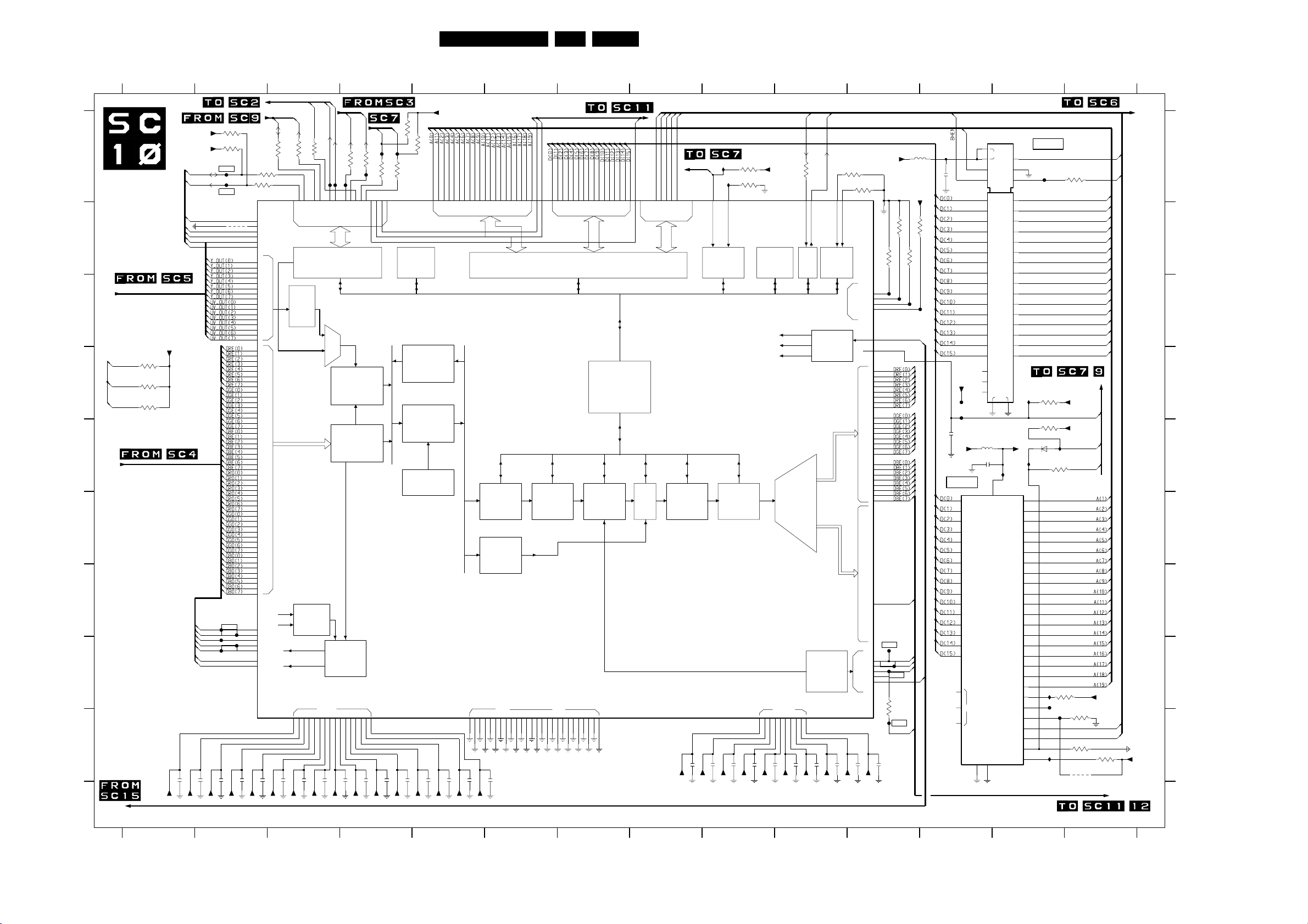
Electrical Diagrams and PWB Layouts
SCAVIO Panel: PW164 Scaler and Memory
1234567891011121314
VPEN
Y_OUT(0:7)
UV_OUT(0:7)
GRE(0:7)
GGE(0:7)
GBE(0:7)
GRO(0:7)
GGO(0:7)
GBO(0:7)
GCLK
ADVS
ADSOG
ADDE
ADHS
GBLKSPL
GCOAST
100n
2601
+2V5
2602
F615
F616
F618
F619
F620
F621
F633
3600
3K3
3601
3K3
100n
+2V5
4605
2603
100n
+2V5
3605
100R
VCLKD12
VCLKEND13
VPENC13
VVSA14
VHSB14
VFIELDA15
VG0D8
VG1C8
VG2B7
VG3A7
VG4B8
VG5D9
VG6C9
VG7A8
VB0B9
VB1A9
VB2B10
VB3A10
VB4D11
VB5A11
VB6C12
VB7B13
GRE0M20
GRE1N19
GRE2N18
GRE3N17
GRE4N20
GRE5P20
GRE6P19
GRE7R20
GGE0F18
GGE1E19
GGE2E20
GGE3J18
GGE4H20
GGE5J19
GGE6J20
GGE7K19
GBE0D16
GBE1A18
GBE2C17
GBE3B18
GBE4A19
GBE5B19
GBE6A20
GBE7D18
GRO0K20
GRO1L17
GRO2L18
GRO3L19
GRO4L20
GRO5M18
GRO6M17
GRO7M19
GGO0E17
GGO1C19
GGO2B20
GGO3C20
GGO4E18
GGO5F17
GGO6D19
GGO7D20
GBO0B15
GBO1A16
GBO2C15
GBO3D15
GBO4B16
GBO5A17
GBO6C16
GBO7B17
GCLKH19
GVSJ17
GHSG19
GPENSOGG20
GFBKH17
GREFH18
GBLKSPLF19
GCOASTF20
2604
3604
PW_SCL_NVM
PW_SDA_NVM
3603
3602
100R
100R
7605
PW164
PORTA0C2PORTA1B1PORTA2B2PORTA3A1PORTA4C4PORTA5D5PORTA6B3PORTA7A2PORTB0A3PORTB1
YUV
TO
RGB
DECODER
AND TIMER
C3
100n
2605
100n
+2V5
+2V5
100R
SYNC
C10
2606
A
SCALER
PW164 +
MEMORY
B
(BASIC
AND ENHANCED
VERSION)
C
VIDEO_SEL_2
VIDEO_SEL_1
D
SYNC_SEL
E
F
G
H
I
{MCLK,DCKEXT}
3122 123 6001.7
+3V3_PW
+3V3_PW
PW_SDA
PW_SCL
CLKOUT_DEINT
VOUT_DEINT
HOUT_DEINT
VFIELD_DEC
+3V3_PW
3625
3K3
3626
3K3
3627
3K3
2600
100n
+2V5
+2V5
123456789101112 13 14
SYNC_SEL
3611
C11
B12
100n
+2V5
VDD2.5
C14
VGA2_EN
VGA2_OUT
100R
F631
F630
F627
I/O
PORTS
VIDEO PORT
PROCESSING
GRAPHICS
PORT PIXEL
PROCESSING
AUTOMATIC
IMAGE
OPTIMIZER
G18
K18
P18
V14
Y14
2607
100n
2608
+2V5
VIDEO_SEL_1
VIDEO_SEL_2
3607
3609
100R
F628
C5
PORTB2D6PORTB3B4PORTB4A4PORTB5C6PORTB6B5PORTB7
PIXEL
OSD
L3
V11V7U5
P3
2609
100n
+2V5
SCL_2
SDA_2
F635
F636
100R
3608
3606
100R
A5
MEMORY IN BUS
G3
100n
100n
2610
+2V5
+2V5
RES
3K3
3612
RES
3K3
3613
100R
16-BIT
MICRO-
PROCESSOR
PROCESSOR
MEMORY
INTERFACE
SDRAM
FRAME
BUFFER
MEMORY
CONTROLLER
2611
100n
2612
+2V5
+3V3_PW
P2
A0P1A1
A2N3A3N4A4R1A5R2A6T1A7T2A8R3A9
2613
100n
+2V5
U2
T3
U1
A13V1A14W1A15V2A16T4A17U3A18Y1A19
A10
A11R4A12
PROCESSOR
MICROPROCESSOR BUS
VERTICAL
IMAGE
SCALAR
ON
SCREEN
DISPLAY
MEMORY OUT BUS
VSS
D10
B11
A12
D14
D17
D4
100n
2614
2615
100n
+2V5
100n
+2V5
{1_2FH,SYNC,FBX_MODE}
A(0:19)
1_2FH
FBX_MODE
W2
PW164
HORIZ.
IMAGE
SCALAR
P17
T19
U17
W17
U14
G17
K17
F3
D0F4D1
D2E1D3F2D4F1D5G2D6G1D7
H3
H1
D8H4D9
ROM/RAM
INTERNAL
REGISTER
INTERFACE
REGISTER BUS
DISPLAY
FIFO
VSS
W14
U12
U11U9U7D7W6W4U4P4L4
K4
G4
49FM242 AB 7.
SYNC
D(0:15)
D10H2D11J1D12J2D13J4D14J3D15
INTERFACE
K1
GAIN
OSD
AND
RD
OSD
2600 I1
2601 I2
2602 I2
2603 I2
2604 I2
2605 I3
2606 I3
2607 I3
2608 I4
2609 I4
2610 I4
2611 I4
2612 I5
A
2613 I5
2614 I5
2615 I6
2616 I8
2617 I9
2618 I9
2619 I9
2620 I9
2621 I10
2622 I10
2623 I10
2624 I11
2625 I11
B
2628 A12
2629 E12
2630 E12
3600 A2
3601 A2
3602 A3
3603 A3
3604 A3
3605 A2
3606 A4
3607 A4
3608 A4
C
3609 A4
3610 H11
3611 A3
3612 A4
3613 A5
3615 A10
3616 A11
3617 A11
3620 B11
3621 B11
3622 B11
D
3623 B11
3625 D1
3626 D1
3627 D1
3628 A14
3630 E13
3631 E13
3632 I14
3633 I14
3634 I14
3636 H14
3637 D13
E
3638 A9
3639 A9
4605 B2
4632 I14
5628 A12
5630 E12
6630 E13
7605 A3
7628 A13
7630 E13
F614 H13
F615 A2
F
F616 A2
F617 D12
F618 G2
F619 G2
F620 H2
F621 H2
F622 D12
F623 C11
F624 C11
F625 C11
F626 C12
G
F627 A4
F628 A4
F629 A13
F630 A3
F631 A3
F632 I13
F633 H2
F634 H11
F635 A4
F636 A4
F637 H11
F638 I11
H
F639 H11
I470 A9
I471 A9
I475 D13
I480 E13
I481 E13
I482 E14
I485 H13
I486 I13
I
ROMOE
BHEN
RAMOE
RAMWE
ROMWE
I470
3639
{PW_START}
N1
L1
K2
M1
L2
M4
M3
N2
WR
CS0M2CS1
BHEN
RAMOE
ROMOE
RAMWE
ROMWE
I471
PW_START
E2
EXTINT
RES
D1
NMI
INTERRUPT
CONTROLLER
1K
3638
1K
+3V3_PW
WATCHDOG
AND
TIMERS
UCLK
DCLK
MCLK
COLOR
LOOKUP
TABLES
COLOR
SPACE
EXPANDER
TXD_PW
RXD_PW
3615
100R
D3
C1
TXD
RXD
UART
DECODERS
TEST
CONTROL
CLOCK
GENERATOR
DISPLAY
TIMING
GENERATOR
IR
3616
D2
IRRCVR0E4IRRCVR1
RES
3617
RES
PTSTEN W3
SCANMODE A13
DTCLK A6
DTMB B6
MCKEXT W13
RESET E3
DRE0 R19
DRE1 T20
DRE2 R18
DRE3 R17
DRE4 T18
DRE5 U19
DRE6 T17
DRE7 V20
DGE0 U18
DGE1 V19
DGE2 W20
DGE3 W19
DGE4 Y20
DGE5 V17
DGE6 U16
DGE7 W18
DBE0 Y19
DBE1 Y18
DBE2 V16
DBE3 U15
DBE4 Y16
DBE5 V15
DBE6 W16
DBE7 W15
DRO0 Y12
DRO1 W11
DRO2 Y11
DRO3 U10
DRO4 V10
DRO5 W10
DRO6 Y10
DRO7 W9
DGO0 Y9
DGO1 W8
DGO2 V8
DGO3 U8
DGO4 Y8
DGO5 Y7
DGO6 W7
DGO7 Y5
DBO0 V6
DBO1 U6
DBO2 W5
DBO3 Y4
DBO4 V5
DBO5 Y3
DBO6 V4
DBO7 Y2
DEN Y15
DHS U13
DVS V13
DCLK W12
DCKEXT Y13
+3V3_PW
3620
F634
F639
PARITY
F637
3621
10K
F623
DEN
DHS
DVS
DCKEXT
100MHZ
10K
3622
F624
MCLK
5628
+3V3_PW
3623
47R
F625
DRE(0:7)DGE(0:7)DBE(0:7)
1K
F626
D(0:15)
100n
2628
2629
+3V3_PW
FLASH
29
31
33
35
38
40
42
44
30
32
34
36
39
41
43
45
A(0)
+3V3
F617
F622
10p
DQ0
DQ1
DQ2
DQ3
DQ4
DQ5
DQ6
DQ7
DQ8
DQ9
DQ10
DQ11
DQ12
DQ13
DQ14
DQ15|A-1
14
13
10
2616
+3V3_PW
2617
100n
+3V3_PW
100n
2618
+3V3_PW
100n
2619
+3V3_PW
C7
C18
100n
2620
+3V3_PW
VDD3.3
U20
V18
Y17
V12V9Y6V3K3
2621
100n
+3V3_PW
100n
2622
+3V3_PW
100n
2623
+3V3_PW
2624
100n
+3V3_PW
100n
2625
+3V3_PW
3610
100n
F638
47R
DCLK
11
VCC
33
39 6
BLE_
40
BHE_
7
I|O1
8
I|O2
9
I|O3
10
I|O4
13
I|O5
14
I|O6
15
I|O7
16
I|O8
29
I|O9
30
I|O10
31
I|O11
32
I|O12
35
I|O13
36
I|O14
37
I|O15
38
I|O16
22
NC1
23
NC2
28
NC3
5630
100MHZ
2630
100n
37
VCC
NC
VSS1
VSS2
46
27
7628
CY62126
17
WE_
CE_
41
OE_
A0
A1
A2
A3
A4
44
A5
43
A6
42
A7
27
A8
26
A9
25
A10
24
A11
21
A12
20
A13
19
A14
18
A15
VSS
1234
+3V3W
I481
I480
7630
M29W160DT
A0
A1
A2
A3
A4
A5
A6
A7
A8
A9
A10
A11
A12
A13
A14
A15
A16
A17
A18
A19
RB_
E_
G_
W_
RP_
BYTE_
SRAM
A(0:19)
RAMWE
F629
3628
RAMOE
100R
5
4
3
2
1
I475
3637
RES
3631
RES
6630
I482
PW_FLASH_RESET
BAT254
3630
1K
A(1)
A(2)
A(3)
A(4)
A(5)
A(6)
A(7)
A(8)
A(9)
A(10)
A(11)
A(12)
A(13)
A(14)
A(15)
A(16)
+3V3_PW
PW_RESET
+3V3W
BOOTWE
25
24
23
22
21
20
19
18
8
7
6
5
4
3
2
1
48
17
16
I485
F614
F632
3636
3K3
3632
3K3
9
15
26
28
11
I486
3633
4K7
4632
RES
12
47
A(0:19)
+3V3W
ROMOE
ROMWE
3634
+3V3W
3K3
CL 36532051_023.eps
140703
Page 50
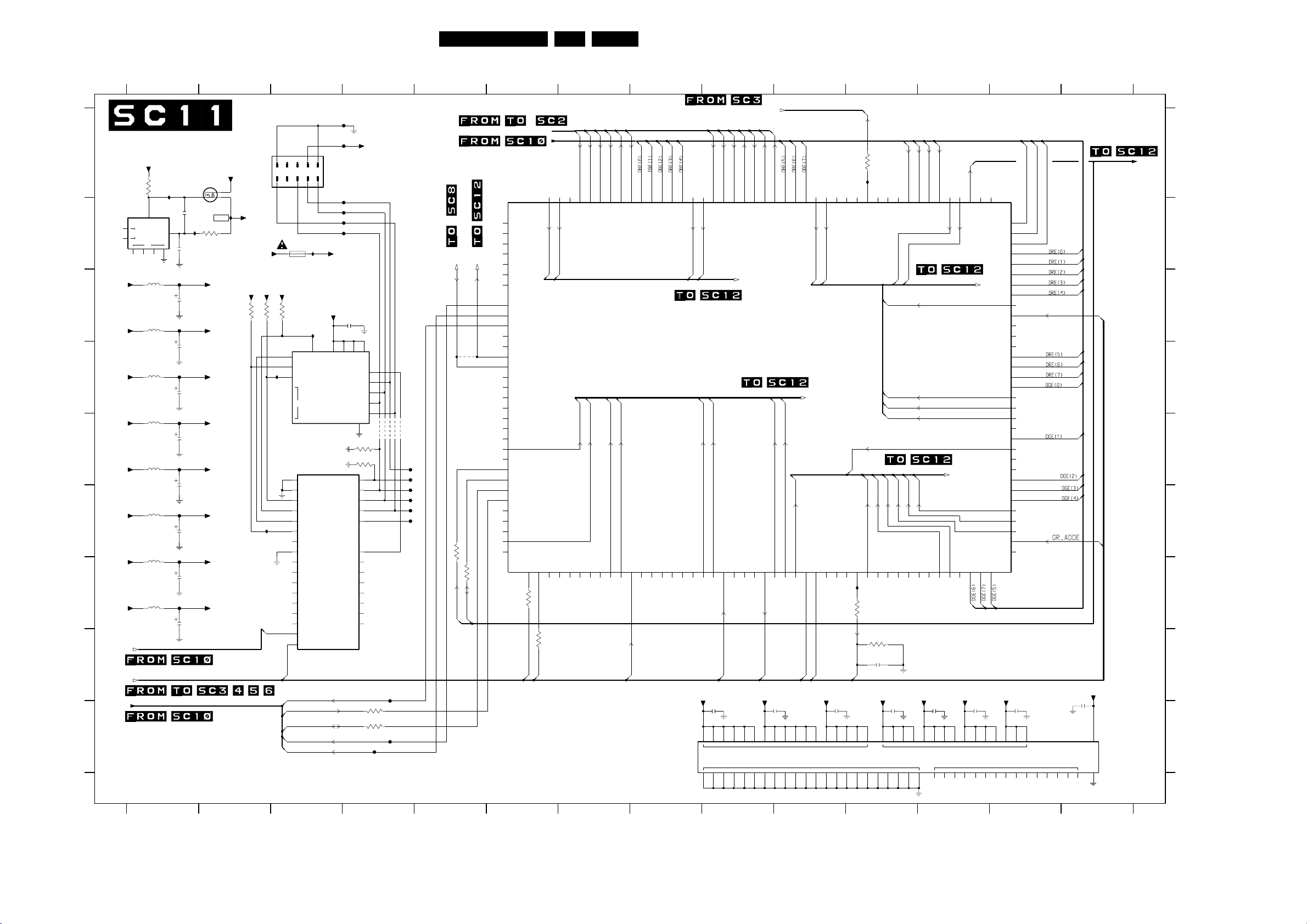
SCAVIO Panel: Back-End EPLD
1234 12 13 14
(BASIC AND ENHANCED VERSION)
A
B
+2V5
C
+2V5
D
+2V5
+3V3_PLD
E
+3V3_PLD
+3V3_PLD
F
+3V3_PLD
G
+3V3_PLD
H
I
3122 123 6001.7
+8V6
7641
I502
8
2641
F646
2642
F647
2643
F648
2644
F649
2645
F650
2646
F651
2647
F652
2648
F653
2649
2640
2V5
100n
I503
1n
10u
10u
10u
10u
10u
10u
10u
10u
STD16NE06L
3641
2K2
3640
4V7
7640
TL431
1
C
5
NC
A
367
5642
100MHZ
5643
100MHZ
5644
100MHZ
5645
100MHZ
5646
100MHZ
5647
100MHZ
5648
100MHZ
5649
100MHZ
REF
2
4
+3V3_PLD
I504
1K
+2V5PLDA
+2V5PLDB
+2V5PLDC
+3V3PLDA
+3V3PLDB
+3V3PLDC
+3V3PLDD
+3V3PLDE
1234567891011
Electrical Diagrams and PWB Layouts
BACK-END-EPLD
6
10
78
9
5
+2V5
1670
+3V3
T 630mA
446
+3V3PLDE
+3V3PLDE
+3V3PLDE
1K
1K
1K
3654
3653
3655
7655
EPC2
4
DCLK
9
CS_
I506
8
OE
6
7
15
NC
16
17
CONTROL
7656-B
EP1K30FC256
P1
MSEL0
R1
MSEL1
T16
STATUS_
N4
CONFIG_
B2
I507
DCLK
DCLK
C15
CONF-DONE
G16
INIT-DONE
B1
CE_
B16
CEO_
B14
WS_
C14
RS_
A16
CS_
A15
CS
G14
RDY-BSY_
D15
CLKUSR
A9
DCP1
L8
DCP2
GR_CLK
FBX_MODE
PW_SCL
PW_SDA
1_2FH
SYNC
F659
+3V3PLDA
F656
2
S85
BYTE BLASTER
0385
CONNECTOR
147279
1
34
F655
F654
F658
F657
I501
+3V3_PLD
L 63V
+3V3PLDE
14
12
13
CASC_
VPPSEL
INIT_|CONF
EEPROM
2655
100n
5
VCCSEL
TRST_
TMS
TCK
TDO
TDI
DATA0
DATA1
DATA2
DATA3
DATA4
DATA5
DATA6
DATA7
18
VPP
DATA
TDO
TCK
TMS
GND
3658
3657
TDI
10K
10K
20
10
R16
P15
B15
C16
C2
A1
B3
A2
C3
B4
A4
D4
B5
I505
VCC
3661
100R
3663
100R
F662
2
1
3
19
11
4657
4658
4655
4659
4656
F640
F641
F642
F643
F644
F645
F660
F661
50FM242 AB 7.
567891011
MATRIX_SEL
3660
POWER_DOWN
POWER_DOWN_EPLD
4654
3662
100R
3664
100R
SCL_1_3V3
SDA_1_3V3
7656-A
EP1K30FC256
B9
DI1
E8
DI2
M9
DI3
R8
DI4
P12
LOCK
D8
DEV_CLR_
C9
DEV-OE
A5
IO1
A6
IO2
A7
IO3
A8
IO4
A10
IO5
A11
IO6
A12
IO7
A13
IO8
B6
IO9
B7
IO10
B8
IO11
B10
IO12
B11
IO13
B12
IO14
B13
IO15
C1
IO16
C4
IO17
C5
IO18
C6
IO19
C8
IO20
C10
IO21
C11
IO22
C12
IO23
C13
IO24
D2
IO25
IO26
D3 D5
3667
VGA2_V
T15
IO148
BLANK_OUT
IO27D6IO28D7IO29
100R
3668
100R
VGA2_H
V_SYNC_POL_N
T12
T13T14
IO145
IO146
IO147
V_SYNC_OUT
R_OUT(6)
IO30D9IO31
D10 D11
V_SYNC_TTL
H_SYNC_TTL
H_SYNC_POL_N
T9
T10
T11
IO142
IO143
IO144
R_OUT(0)
R_OUT(1)
IO32
IO33
IO34
D13
D14
H_HD
75OHM_ON
V_SYNC_CMP
T7
T6
IO140
IO141
IO139
T4T5
IO138
T3
IO137
T2
IO136
T1
IO135
H_SYNC_CMP
R13
R14
R15
IO132
IO133
IO134
PARITY_OUT
H_SYNC_OUT
V_SYNC_LM
C_SYNC_LM
C_SYNC_OUT
R10
R11R12
IO130
IO131
H_PRESENT
R9
IO128
IO129
R7
IO127
I/O PORT PROCESSING
R_OUT(4)
R_OUT(2)
IO36E2IO37
IO35
D16
E1
VGA1_V
IO38
E4 E7
IO39
R_OUT(3)
IO40
IO41
IO42
IO43
IO44F1IO45
E9
E10
E13
+2V5PLDA
VCCINT
GND
IO46
E14
E15
F2 F3
VGA1_H
2656
100n
E11 J10 J11 K9 L5 L7 L12 M11R2F5 F7 F9 F12
A3 G10 H8
IO47F4IO48
IO49
F13
ALT_GR_ADDE
+2V5PLDB
2657
100n
H6 H7 H10 J7 D12
7656-C
EP1K30FC256
F11 G7 G9 T8
V_HD
R5
R6
IO125
IO126
R_OUT(5)
R_OUT(7)
IO50
IO51
F15
F14
P14
P16
R3
R4
IO121
IO122
IO123
IO124
B_OUT(4)
B_OUT(5)
G_OUT(0)
IO52G1IO53G2IO54G4IO55G5IO56
F16
HD_CLAMPN
HD_BLANKN
+2V5PLDC
2658
100n
P13
IO120
P10
P11
IO118
IO119
G_OUT(5)
IO57
IO58
G12
G13G15
I511
3665
TV_MODE
100R
I510
P9
IO117
G_OUT(1)
IO59
100R
3666
RES
2666
RES
+3V3PLDA
P6
P7
P8
IO114
IO115
IO116
B_OUT(3)
B_OUT(1)
B_OUT(7)
B_OUT(6)
B_OUT(0)
G_OUT(7)
G_OUT(6)
G_OUT(2)
IO60
IO61
IO62H5IO63
H2
H3 H4
2659
100n
VCCIO
GROUND AND SUPPLY
DEN
PARITY
P4
P5
IO112
IO113
B_OUT(2)
G_OUT(4)
G_OUT(3)
IO64
H12
+3V3PLDB
DHS
2660
100n
IO111
IO65
H13
DVS
NC
D1 K16 L2 L4 M14M16N15E3 E16 G3 H1 H16H9 J8 J9 K5 K7 K10 L1 L6A14 L11 M5 M12C7 E5 E12 F6
P2P3
IO110
IO66
H14 H15
SYNC_SEL
VIDEO_SEL_1
VIDEO_SEL_2
PWRDWN_LVDS
N10
N11
N13
N14
N16
IO105
IO106
IO107
IO108
IO109
IO67J2IO68J3IO69
+3V3PLDC
G11H11 J6
2661
100n
K6 K8 K11 L10 M6 N12E6 F8 F10 G6 G8
IO70
J4 J5
IO104
IO103
IO102
IO101
IO100
IO99
IO98
IO97
IO96
IO95
IO94
IO93
IO92
IO91
IO90
IO89
IO88
IO87
IO86
IO85
IO84
IO83
IO82
IO81
IO80
IO79
IO78
IO77
IO76
IO75
IO74
IO73
IO72
IO71
+3V3PLDD
J1 K3 K14
N9
N8
N7
N6
N5
N3
N2
N1
M15
M13
M10
M8
M7
M4
M3
M2
M1
L16
L15
L14
L13
L3
K15
K13
K12
K4
K2
K1
J16
J15
J14
J13
J12
2662
100n
DRE(0:7)
VIDCLK
DGE(0:7)
+2V5PLDC
2663
100n
VCC_CKLK
GND_CKLK
12 13 14
L9
CL 36532051_024.eps
140703
0385 A3
1670 B3
2640 B1
2641 B1
2642 C1
2643 D1
2644 D1
2645 E1
2646 F1
2647 F1
2648 G1
2649 G1
A
2655 C4
2656 I9
2657 I10
2658 I10
2659 I11
2660 I12
2661 I12
2662 I13
2663 I14
2666 H11
3640 A1
3641 B2
3653 C2
B
3654 C2
3655 C3
3657 E4
3658 E4
3660 A11
3661 I4
3662 F5
3663 I4
3664 G5
3665 G11
3666 H11
3667 G6
C
3668 H6
4654 D5
4655 E4
4656 E4
4657 E4
4658 E4
4659 E4
5642 C1
5643 C1
5644 D1
5645 E1
5646 E1
D
5647 F1
5648 G1
5649 G1
7640 B1
7641 A2
7655 D3
7656-A A6
7656-B E3
7656-C I9
F640 E4
F641 E4
E
F642 F4
F643 F4
F644 F4
F645 F4
F646 C1
F647 C1
F648 D1
F649 E1
F650 E1
F651 F1
F652 G1
F653 G1
F
F654 B4
F655 B4
F656 A4
F657 B4
F658 B4
F659 A4
F660 H4
F661 I4
F662 I4
I501 B3
I502 A1
I503 B1
G
I504 B2
I505 C3
I506 D3
I507 F2
I510 A11
I511 G11
H
I
Page 51
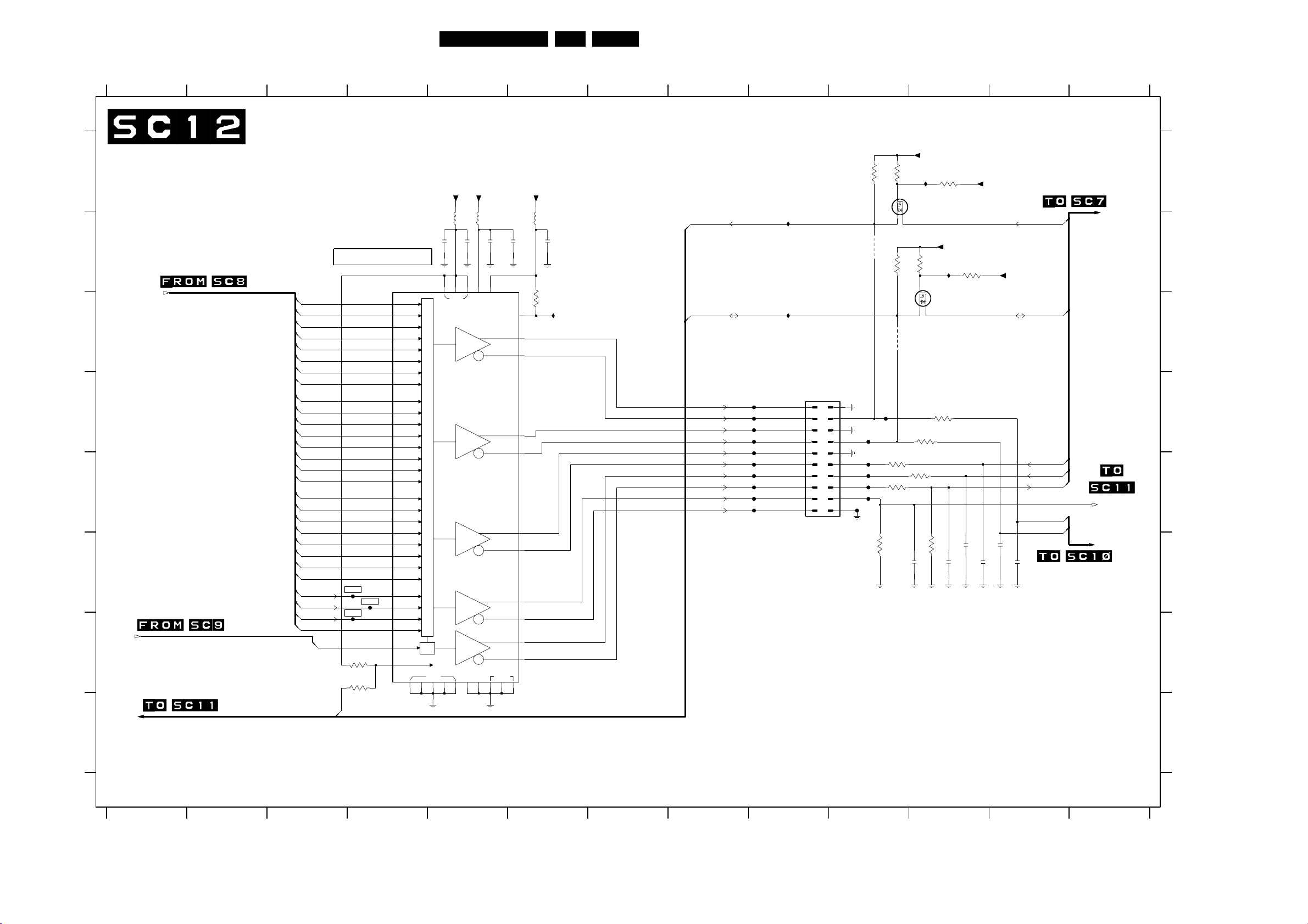
Electrical Diagrams and PWB Layouts
SCAVIO Panel: Back-End LVDS Output
123456
BACK-END-LVDS-OUTPUT
(BASIC AND ENHANCED VERSION)
A
B
C
D
E
F
G
R_OUT(0)
R_OUT(1)
R_OUT(2)
R_OUT(3)
R_OUT(4)
R_OUT(7)
R_OUT(5)
G_OUT(0)
G_OUT(1)
G_OUT(2)
G_OUT(6)
G_OUT(7)
G_OUT(3)
G_OUT(4)
G_OUT(5)
B_OUT(0)
B_OUT(6)
B_OUT(7)
B_OUT(1)
B_OUT(2)
B_OUT(3)
B_OUT(4)
B_OUT(5)
PARITY_OUT
H_SYNC_OUT
V_SYNC_OUT
BLANK_OUT
R_OUT(6)
DCLK
LVDS ENCODER
7670
DS90C385MTD
51 TXIN0
52 TXIN1
54 TXIN2
55 TXIN3
56 TXIN4
2 TXIN5
3 TXIN6
4 TXIN7
6 TXIN8
7 TXIN9
8 TXIN10
10 TXIN11
11 TXIN12
12 TXIN13
14 TXIN14
15 TXIN15
16 TXIN16
18 TXIN17
19 TXIN18
20 TXIN19
22 TXIN20
23 TXIN21
24 TXIN22
25 TXIN23
F690
F692
3675
PWRDWN_LVDS
10K
3679
100R
F691
3V3
27 TXIN24
28 TXIN25
30 TXIN26
50 TXIN27
TXCLKIN31
32 PWRDWN_
5
+3V3_PW
+3V3_PW
5672
5670
2670
100n
VCC
TTL PARALLEL-TO-LVDS
TTL PARALLEL-TO-LVDS
PLL
GND
13 21 29 53 36 43 49
100MHZ
2671
2691
PLL
GND
35 33
100MHZ
100n
2672
34
PLLVCC
100n
44
R-FB 17
LVDSVCC
LSVD
GND
2674
100n
48TXOUT0-
47TXOUT0+
46TXOUT1-
45TXOUT1+
42TXOUT2-
41TXOUT2+
38TXOUT3-
37TXOUT3+
40TXCLKOUT-
39TXCLKOUT+
+3V3_PW
5673
3673
100MHZ
100n
2673
10K
I685
51FM242 AB 7.
7 8 9 10 11 12 13
+3V3_STBY_SW
3K3
3686
SCL_1_3V3
SDA_1_3V3
F670
F671
F672
F673
F674
F675
F676
F677
F678
I682
I683
TxOut0_m
TxOut0_p
TxOut1_m
TxOut1_p
TxOut2_m
TxOut2_p
TxCLKOut_m
TxCLKOut_p
TxOut3_m
TxOut3_p
S01
PDP INTERFACE
CONNECTOR
19
17 18
15 16
13 14
11 12
9
78
56
34
1
DF13
0301
20
F681
F682
10
F683
F684
F685
F686F679
2
3685
4684
F680
3670
3681
4680
3674
100R
3677
100R
RES
470R
I680
7675
BSH103
3K3
3682
470R
7676
BSH103
3671
3672
RES
3676
100R
3687
26941p2695
3688
RES
+3V3_STBY_SW
I681
RES
RES
2696
1p
3689
RES
1p
+5V_STBY_SW
2698
1p
2697
+5V_STBY_SW
1p
1p
2699
SCL_1
SDA_1
CPU_GO
PDP_GO
IRQ_PDP
POWER_DOWN_EPLD
PW_SCL
PW_SDA
A
B
C
D
G
0301 E9
2670 B5
2671 B5
2672 B5
2673 B6
2674 B6
2694 F11
2695 F11
2696 F11
2697 F11
2698 F12
2699 F12
3670 F10
3671 D11
3672 D11
3673 C6
3674 E10
3675 G4
3676 E11
3677 E10
3679 G4
3681 B10
3682 B11
3685 A10
3686 A10
3687 F11
3688 A11
3689 B11
4680 C10
4684 B10
5670 B5
5672 B5
5673 B6
7670 B4
7675 A11
7676 B11
F670 D9
F671 D9
F672 D9
F673 D9
F674 D9
F675 E9
F676 E9
F677 E9
F678 E9
F679 E9
F680 D10
F681 D10
F682 E10
F683 E10
F684 E10
F685 E10
F686 E10
F690 F4
F691 F4
F692 G4
I680 A11
I681 B11
I682 B9
I683 C9
E
I685 C6
F
H
3122 123 6001.7
1
23456
78
H
CL 36532051_025.eps
140703
9 10111213
Page 52
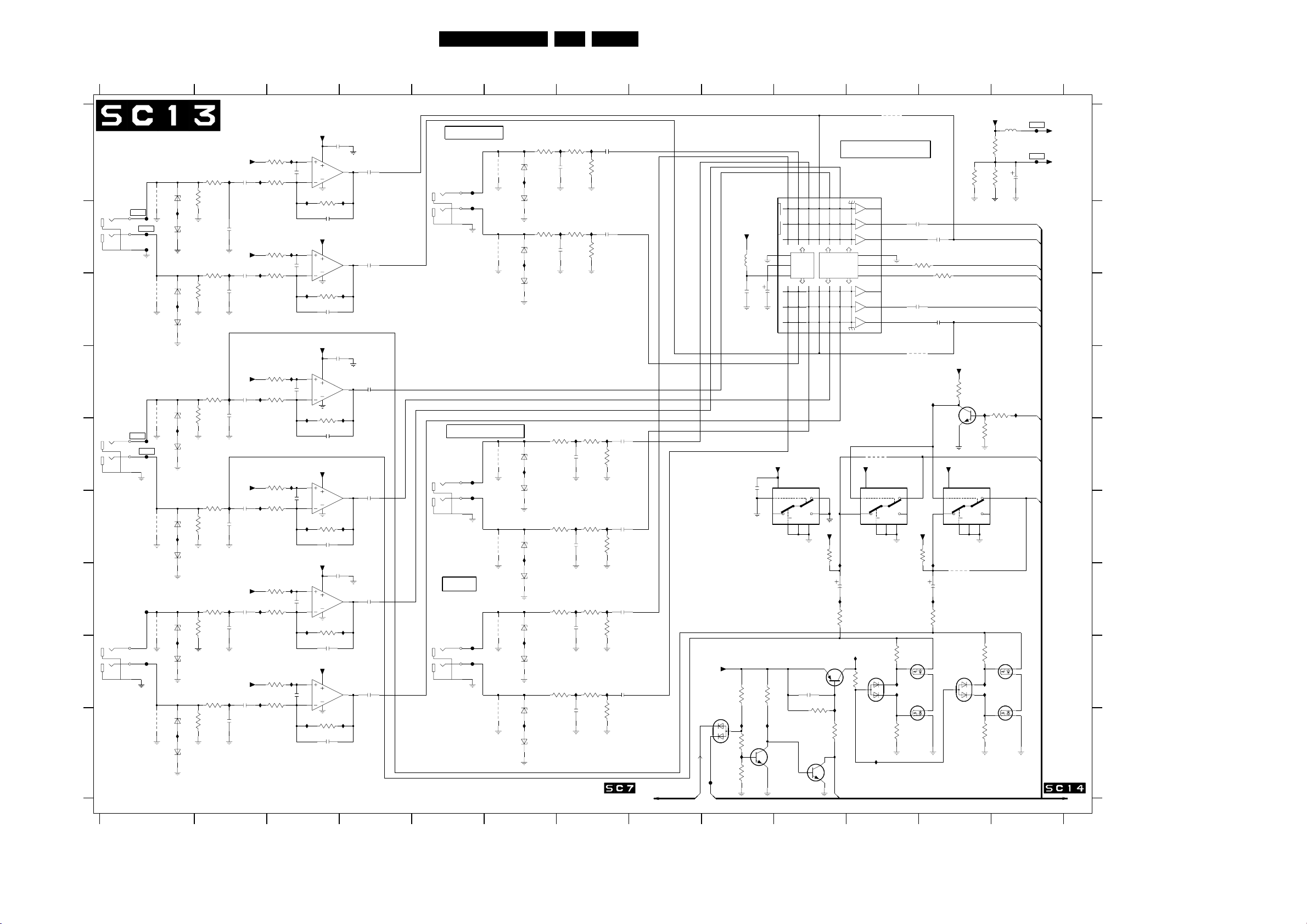
Electrical Diagrams and PWB Layouts
SCAVIO Panel: Audio Source Select
1 2345678910111213
AUDIO SOURCE SELECT
(BASIC AND ENHANCED VERSION)
A
+4V3A
I532
I531
2712
3711
1K
AUDIO_VGA_IN
0378-A
COMBI
F710
1
B
S77
3
2
C
D
AUDIO_FLEX_VGA
0378-B
COMBI
F713
S77
4
6
5
E
F
G
AUDIO_DVI
0378-C
COMBI
7
S77
9
8
H
I
3122 123 6001.7
F711
F712
F714
F715
L
F716
1
3710
BZM55-C33
BZM55-C33
3720
BZM55-C33
BZM55-C33
3730
BZM55-C33
BZM55-C33
3740
BZM55-C33
BZM55-C33
3750
BZM55-C33
BZM55-C33
3760
BZM55-C33
BZM55-C33
33K
3721
33K
3731
330R
33K
3741
330R
33K
3751
33K
3761
33K
RES
471047304750
6710
I537
L
6711
R
RES
47204740
6720
I547
6721
RES
6730
I554
L
6731
R
RESRES
6740
I567
6741
6750
I580
6751
R
RES
4760
6760
I598
6761
1u
2711
100p
+4V3A
I543
I542
2722
1K
1u
100p
2721
+4V3A
I549
I550
2732
1u
2731
100p
+4V3A
I561
I562
2742
1u
100p
2741
+4V3A
I573
I572
2752
1K
1u
2751
100p
+4V3A
I591
I590
2762
1K
1u
100p
2761
2345678910111213
3713
100R
3714
22K
3723
100R
3724
22K
3733
100R
3734
22K
3743
100R
3744
22K
3753
100R
3754
22K
3763
100R
3764
22K
I530
I541
I548
I559
I571
I583
2714
2724
2734
2744
2754
2764
3V9
3V9
3V9
3V9
I535
I545
I551
I563
I578
I593
3
RES
2
5
RES
6
3
RES
2
5
RES
6
3
RES
2
5
RES
6
+8V6A
2716
+8V6A
2726
+8V6A
2736
+8V6A
2746
+8V6A
2756
+8V6A
2766
8
4
3716
15K
47p
8
4
3726
15K
47p
8
4
3736
15K
47p
8
4
3746
15K
47p
8
4
3756
15K
47p
8
4
3766
15K
47p
2715
100n
7714-A
LM833DT
3V9
I536
7714-B
LM833DT
3V9
I546
2735
100n
7734-A
LM833DT
I552
7734-B
LM833DT
I564
2755
100n
7754-A
LM833DT
I579
7754-B
LM833DT
I594
52FM242 AB 7.
0378-A B1
0378-B E1
0378-C G1
0379-B A5
4794
AV1 CVBS
I534
I533
I538
I544
I560
I568
I581
I597
6770
6771
6774
6775
6778
6779
6782
6783
6786
6787
6790
6791
3771
1K
BZM55-C33
BZM55-C33
3775
1K
BZM55-C33
BZM55-C33
BZM55-C33
BZM55-C33
BZM55-C33
BZM55-C33
BZM55-C33
BZM55-C33
BZM55-C33
BZM55-C33
2771
I539
2775
3779
1K
3783
1K
3787
1K
3791
1K
100p
100p
COMBINED WITH
CVBS + Y INPUT
2717
1
1u
2727
7
1u
2737
1
1u
2747
7
1u
ON SC 2
AUDIO_CVBS
0379-B
COMBI
F717
4
F718
6
5
S79
AV2 AUDIO YC
COMBINED WITH
CVBS + Y INPUT
ON SC 2
AUDIO_YC
0379-C
COMBI
F719
7
F720
9
8
S79
RESRESRES
4770
L
R
L
R
RESRES
AV3
2757
1
1u
2767
7
1u
COMBINED WITH
PR + PB + H_HD_EXT
+ V_HD_EXT
ON SC 2
AUDIO_YPbPr
0380-A
COMBI
S80
F721
1
F722
3
2
47864790 4782 4778 4774
L
R
RES
2772
3772
3K3
10K
3773
I540
2776
3776
3K3
10K
3777
I557
I558
3780
3K3
100p
2779
I565 I566
3784
3K3
100p
2783
I576 I577
3788
3K3
2787
100p
I587
I586
3792
3K3
2791
100p
1u
1u
3781
3785
3789
3793
10K
10K
10K
10K
2780
2784
2788
2792
1u
1u
1u
1u
{POWER_OK}
6802
BAW56W
2
1
F725
POWER_OK
+9V_STBY
3
0V6
I599
D_CTR_ONE
3802
3820
3821
+8V6
5798
2798
I595
100MHZ
100n
2801
33K
33K
10K
7798
TEA6422D
2799
+8V6A
100n
9
4
3822
7801
BC847BW
22
21
I596
NC
8
7
GND
1
CAP
2
VS
3
22u
16
Vdd
S
Z
33K
0V
4L15L26
L39L410L511L6
SUPPLY BUS DECODER
R124R223R320R419R5
25
7800-C
74HC4053D
Y0
5
Y1
3
E
Vee8Vss
6
7
+4V3A
3836
100K
2802
3800
7803
BC857BW
2804
7802
BC847BW
8V5
1n
3803
I592
100K
3804
AUDIO_ENABLE
MATRIX SWITCH
LOUT3
16
LOUT2
14
LOUT1
12
ADDR
26
SCL
27
SDA
28
ROUT3
17
ROUT2
15
ROUT1
I582
11
14
3809
+8V6A
Vdd
S
Z
0V9
33K
3
4800
7800-A
74HC4053D
16
E
6
6805
BAW56W
I525
13
Vee8Vss
7
0V
1
2
0V
3805
3806
Y0
Y1
100K
I584
I588
100K
12
13
BSH103
8V5
R6
18
I569
10u
I574
330R
33K
2794
1u
3794
100R
2796
1u
4797
+4V3A
7805
BSH103
7806
3837
I553
100K
2803
3801
0V
2795
1u
3795
100R
2797
1u
BC847BW
+8V6A
Vdd
S
10
Z
15
I570
10u
I575
330R
+8V6A
3719
7718
16
4801
BAW56W
3
3798
33K
7800-B
74HC4053D
Vee7Vss
E
6
6807
+8V6
3796
33K
3797
I555
3717
33K
10K
3718
Y0
2
Y1
1
8
3807
100K
BSH103
0V
1
I585
2
I589
BSH103
0V
3808
100K
5796
100MHZ
4K7
4K7
7807
7808
2800
100u
PRE_OUT2_L
PRE_OUT1_L
SCL_AUDIO
SDA_AUDIO
PRE_OUT2_R
PRE_OUT1_R
I556
D_CTR_NIL
SC1_R
SC1_L
0V
F723
+8V6A
F724
+4V3A
CL 36532051_026.eps
140703
0379-C E5
0380-A G5
2711 B2
2712 A2
2714 A3
2715 A3
2716 B3
2717 A4
A
2721 C2
2722 B2
2724 B3
2726 C3
2727 B4
2731 D2
2732 D2
2734 D3
2735 D3
2736 E3
2737 D4
2741 F2
2742 F2
2744 F3
B
2746 F3
2747 F4
2751 G2
2752 G2
2754 G3
2755 G3
2756 H3
2757 G4
2761 I2
2762 H2
2764 H3
C
2766 I3
2767 H4
2771 A6
2772 A7
2775 B6
2776 B7
2779 E7
2780 E7
2783 F7
2784 F7
2787 G7
2788 G7
D
2791 I7
2792 H7
2794 B11
2795 B12
2796 C11
2797 C12
2798 C9
2799 C9
2800 A13
2801 E9
2802 G10
2803 G12
E
2804 H10
3710 A2
3711 A2
3713 A3
3714 A3
3716 A3
3717 D13
3718 E12
3719 D12
3720 C2
3721 B2
F
3723 B3
3724 B3
3726 C3
3730 D2
3731 D2
3733 D3
3734 D3
3736 D3
3740 F2
3741 F2
3743 E3
3744 F3
G
3746 F3
3750 G2
3751 G2
3753 G3
3754 G3
3756 G3
3760 I2
3761 H2
3763 H3
3764 H3
3766 I3
3771 A6
H
3772 A7
3773 A7
3775 B6
3776 B7
3777 B7
3779 E7
3780 E7
3781 E7
3783 F7
3784 F7
3785 F7
3787 G7
3788 G7
I
3789 G7
3791 H7
3792 H7
3793 I7
3794 B12
3795 B12
3796 A13
3797 A13
3798 A12
3800 G10
3801 G12
3802 H9
3803 H10
3804 I10
3805 H11
3806 I11
3807 H12
3808 I12
3809 H11
3820 I9
3821 I9
3822 H9
3836 F10
3837 F12
4710 A1
4720 C1
4730 D1
4740 F1
4750 G1
4760 I1
4770 A6
4774 B6
4778 E6
4782 F6
4786 G6
4790 I6
4794 A11
4797 D11
4800 E11
4801 G12
5796 A13
5798 B9
6710 A1
6711 B1
6720 C1
6721 C1
6730 D1
6731 E1
6740 F1
6741 F1
6750 G1
6751 H1
6760 I1
6761 I1
6770 A6
6771 A6
6774 B6
6775 C6
6778 E6
6779 E6
6782 F6
6783 G6
6786 G6
6787 H6
6790 I6
6791 I6
6802 I9
6805 H11
6807 H12
7714-A A3
7714-B B3
7718 D12
7734-A D3
7734-B E3
7754-A G3
7754-B H3
7798 A9
7800-A E11
7800-B E12
7800-C E10
7801 I9
7802 I10
7803 H10
7805 H11
7806 H12
7807 H13
7808 H13
F710 B1
F711 B1
F712 B1
F713 E1
F714 E1
F715 G1
F716 H1
F717 A5
F718 B5
F719 E5
F720 F5
F721 H5
F722 H5
F723 A13
F724 A13
F725 I9
I525 I11
I530 A3
I531 A2
I532 A2
I533 A7
I534 A7
I535 A3
I536 A4
I537 B1
I538 A6
I539 B7
I540 B7
I541 B3
I542 B2
I543 B2
I544 B6
I545 C3
I546 C4
I547 C1
I548 D3
I549 D2
I550 D2
I551 D3
I552 D4
I553 D12
I554 E1
I555 D12
I556 D13
I557 E7
I558 E7
I559 E3
I560 E6
I561 F2
I562 F2
I563 F3
I564 F4
I565 F7
I566 F7
I567 F1
I568 F6
I569 G11
I570 G12
I571 G3
I572 G2
I573 G2
I574 G11
I575 G12
I576 G7
I577 G7
I578 G3
I579 G4
I580 H1
I581 H6
I582 H11
I583 H3
I584 H11
I585 H13
I586 H7
I587 H7
I588 H11
I589 H13
I590 H2
I591 H2
I592 I10
I593 I3
I594 I4
I595 I9
I596 I10
I597 I6
I598 I1
I599 I9
Page 53
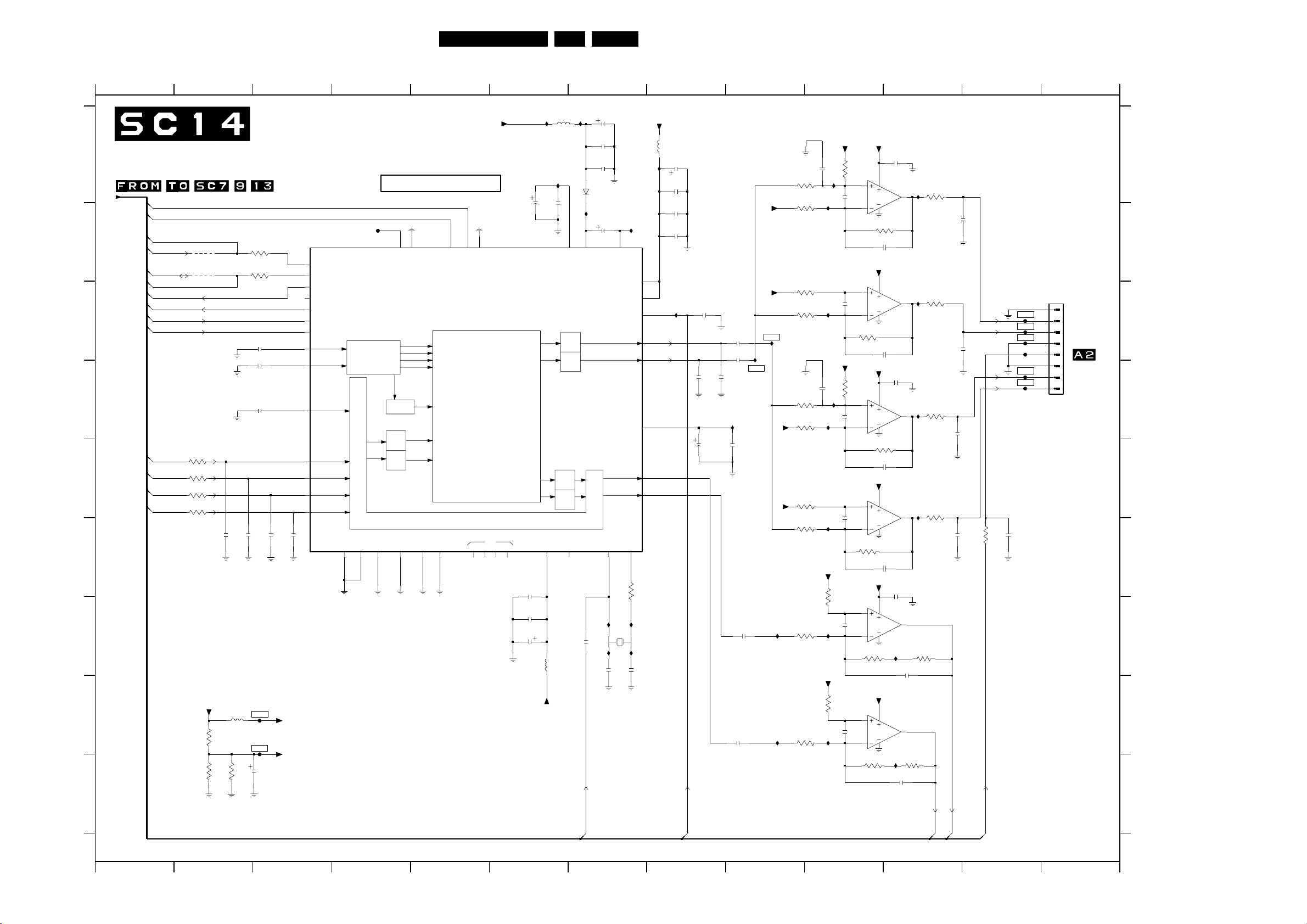
SCAVIO Panel: Audio Processor
1234 12 13
A
D_CTR_NIL
D_CTR_ONE
B
C
SCL_AUDIO
SCL_SW
SDA_SW
SDA_AUDIO
I2S_CLOCK
I2S_DATA_OUT
I2S_DATA_IN1
I2S_DATA_IN2
4810
4811
D
PRE_OUT1_R
E
PRE_OUT1_L
PRE_OUT2_R
PRE_OUT2_L
3815
100R
3816
100R
3817
100R
3818
100R
2811
1n
2815
F
G
+8V6
3810
3814
4K7
RES
5810
100MHZ
4K7
3811
H
I
3122 123 6001.7
123456789
Electrical Diagrams and PWB Layouts
AUDIO PROCESSOR
(BASIC AND ENHANCED VERSION)
AUDIO PROCESSOR
F820
7812
2810
3812
100R
3813
100R
2812
1n
2813
1n
2814
100n
1n
F810
F811
2818
100u
1n
+8V6B
+4V3B
12 I2C_CL
13 I2C_DA
15 I2S_WS
17 I2S_DA_IN1
3 ANA_IN-
2 ANA_IN+
41 SC1_IN_R
3V8
40
3V8
38 SC2_IN_R
3V8
37 SC2_IN_L
3V8
1n
2819
MSP3415G
I2S_CL14
I2S_DA_OUT16
I2S_DA_IN221
MONO_IN43
SC1_IN_L
DEMODULATOR
VREF1
VREF2
25
A/D
A/D
AHVSS
35
IDENT
ASG
18 10
ADR_CL
ADR_SEL
39
53FM242 AB 7.
567891011
I651
100n
42
VREFTOP
D/A
D/A
TP
729
6820
I691
2869
2821
10u
2822
1n5
2838
470p
BAT254
2820
10u
33
AHVSUP
34
CAPL_M
STBYQ
DVSUP
RESETQ
DACM_R 26
LOUDSPEAKER
XTAL_IN
56
I667
1835
1n5
RES
I672
RES
2835
VXCA_18M432
I692
XTAL_OUT
3835
I668
I673
2836
RES
RES
11
19
22
27DACM_L
36AGNDC
30SC1_OUT_R
31SC1_OUT_L
I652
+5V
5822
0V2
0V2
100MHZ
3V8
3V8
10u
2823
2824
1n5
2839
470p
2845
220p
I678
2831
100n
2828
2829
MSP_RESET
1n
10u
2825
1n
I663
2830
2826
1u
2827
1u
2863
1u
100n
2868
1u
I660
+4V3B
+4V3B
I659
I669
I674
+4V3B
+4V3B
3840
22K
3841
22K
3845
100R
3846
22K
3850
22K
3851
22K
3855
100R
3856
22K
3861
22K
3864
22K
2840
I656
I658
2850
I664
I666
+4V3B
3866
I670
+4V3B
3867
I675
I654
I661
27p
27p
+4V3B
3848
2841
2846
+4V3B
3858
2851
2856
100R
2859
100R
2864
4V2
4V2
4V2
4V2
4V2
4V2
4V2
4V2
4V2
4V2
4V2
4V2
39K
RES
RES
39K
RES
RES
RES
RES
3
2
5
6
3847
39K
3
2
5
6
3857
39K
3
2
5
6
+8V6B
+8V6B
+8V6B
+8V6B
+8V6B
3862
27K
+8V6B
3865
27K
8
4
3843
39K
2843
27p
8
4
2848
27p
8
4
3853
39K
2853
27p
8
4
2858
27p
8
4
8
4
2842
100n
7841-A
LM833DT
4V2
7841-B
LM833DT
4V2
2852
100n
7851-A
LM833DT
4V2
7851-B
LM833DT
4V2
2861
100n
7861-A
TS462CD
4V2
I671
2862
47p
7861-B
TS462CD
4V2
I676
2865
47p
I655
3844
1
100R
I657
3849
7
100R
I662
3854
1
100R
I665
3859
7
100R
1
7
3863
8K2
L
3860
8K2
R
SC1_R
AVSS
44
FM1
FM2
NICAM A
NICAM B
IDENT
SCART-L
SCART-R
SCART
DVSS
20
8
9
D_CTR_IO0
D_CTR_IO1
I2SL/R
S1...4
Switching Facilities
+8V6
4
TESTEN
I2SL/R
LOUDSPEAKER R
LOUDSPEAKER L
DFP
HEADPHONE R
HEADPHONE L
NC
23 24 28 32
2816
SCART-R
SCART-L
2837
470p
2833
1n5
2834
10u
I650
10u
5834
+5V
5820
100MHZ
I653
2817
D/A
D/A
AVSUP
1
100MHZ
10 11 12 13
L_POS
2844
L_NEG
2849
R_POS
2854
R_NEG
2857
SC1_L
1n
1n
1n
1n
3870
2867
100R
AUDIO_ENABLE
AUDIO OUTPUT
S88
8
F812
7
F813
6
F814
5
F815
4
3
F816
2
F817
1
0388
PH-S
220n
CL 36532051_027.eps
TO
0388
140703
0388 D13
1835 G7
2810 I2
2811 F2
2812 C3
2813 D3
2814 D3
2815 F2
2816 B6
2817 B6
2818 F3
2819 F3
A
2820 B7
2821 A7
2822 A7
2823 A8
2824 A8
2825 D8
2826 C9
2827 C9
2828 D8
2829 E8
2830 E9
2831 C8
2833 G6
B
2834 G6
2835 G7
2836 G7
2837 F6
2838 A7
2839 B8
2840 A10
2841 A10
2842 A11
2843 B11
2844 B11
C
2845 B8
2846 C10
2848 C11
2849 C11
2850 D10
2851 D10
2852 D11
2853 E11
2854 D11
2856 F10
2857 F11
2858 F11
D
2859 G10
2861 F11
2862 G11
2863 H9
2864 H10
2865 I11
2867 F12
2868 G9
2869 G7
3810 H2
3811 I2
3812 B3
E
3813 B3
3814 I2
3815 E2
3816 E2
3817 E2
3818 E2
3835 F7
3840 A10
3841 B10
3843 B11
3844 A11
F
3845 C10
3846 C10
3847 C10
3848 A10
3849 C11
3850 D10
3851 D10
3853 E11
3854 D11
3855 E10
3856 F10
3857 F10
G
3858 D10
3859 E11
3860 G11
3861 G10
3862 G10
3863 I11
3864 H10
3865 I10
3866 F10
3867 H10
3870 F12
4810 B2
H
4811 B2
5810 H2
5820 A6
5822 A8
5834 G6
6820 A7
7812 B3
7841-A A11
7841-B C11
7851-A D11
7851-B E11
I
7861-A G11
7861-B H11
F810 H3
F811 H3
F812 C12
F813 C12
F814 C12
F815 C12
F816 D12
F817 D12
F820 B4
I650 A6
I651 A7
I652 A8
I653 A6
I654 A10
I655 A11
I656 A10
I657 C11
I658 C10
I659 C9
I660 D9
I661 D10
I662 D11
I663 D9
I664 D10
I665 E11
I666 F10
I667 G7
I668 G7
I669 G9
I670 G10
I671 G11
I672 G7
I673 G7
I674 H9
I675 H10
I676 I11
I678 C8
I691 B7
I692 B7
Page 54
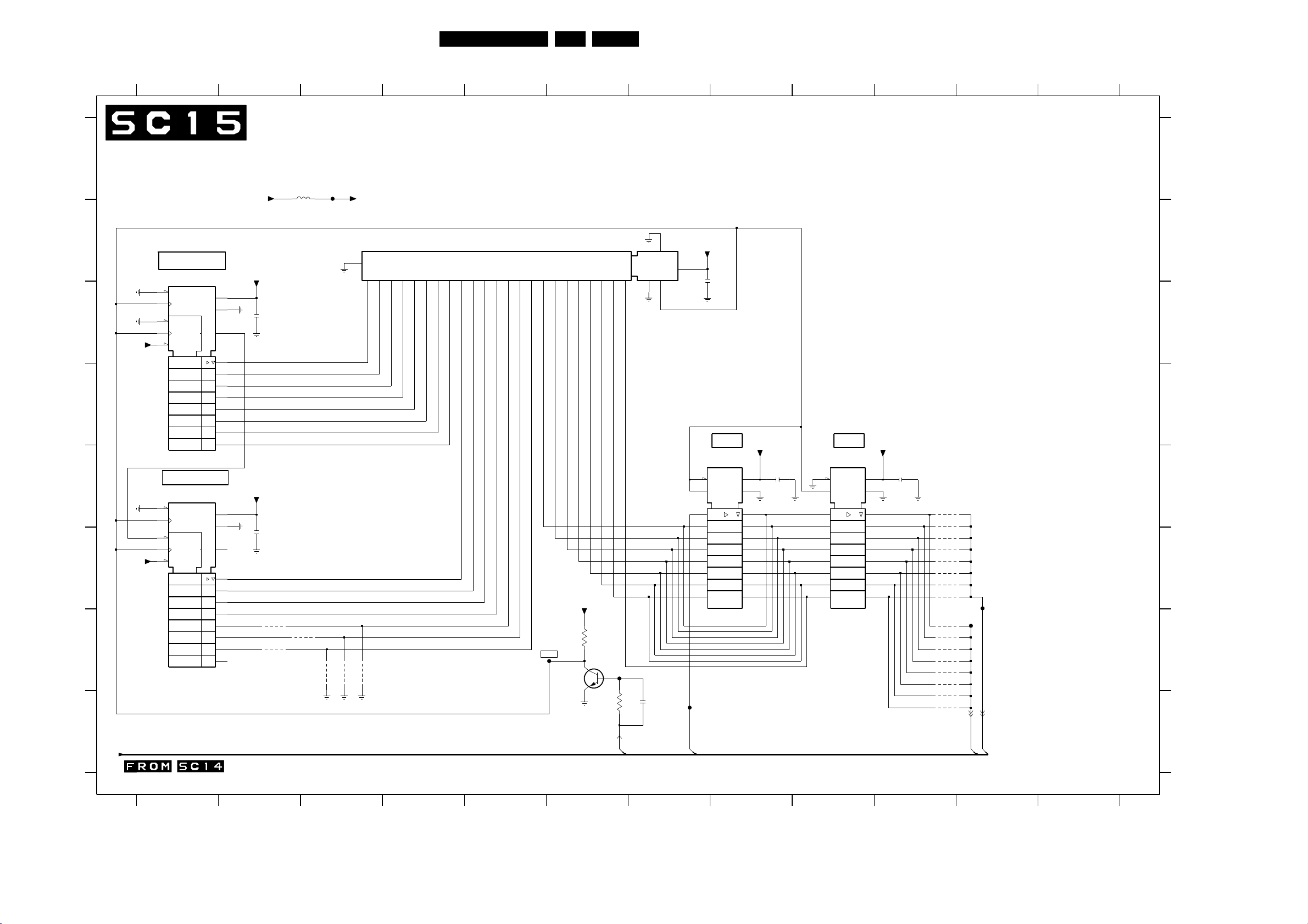
Electrical Diagrams and PWB Layouts
SCAVIO Panel: Audio Delay Line
1234567
A
B
COUNTER
7870
TC74HC590AF
14
C
D
G
EN3
13
C2
12
G1
CTR8
11
(CT=255)Z4
1+
10
+5D
E
F
+5D
CT=0
COUNTER
7874
TC74HC590AF
14
EN3
13
C2
12
G1
CTR8
11
(CT=255)Z4
1+
10
CT=0
VCC
GND
2D 3
VCC
GND
2D 3
16
8
9
4
15
1
2
3
4
5
6
7
16
8
9
4
15
1
2
3
4
5
6
7
AUDIO DELAY LINE
(BASIC AND ENHANCED VERSION)
F870
+5D
2870
+5D
2874
+5V
5870
100MHZ
100n
100n
4871
4872
4873
4874
4875
+5D
7880
CY7C199B
14
4876
GND
A1
21A023
24A225A326
A41A52A63A7
A85A9
4
RAM
A107A11
6
A12
8
A1310A14
9
I|O215I|O316I|O417I|O518I|O619I|O7
I|O1
I|O0
12
13
11
F872
7879
BC847BW
+5D
3880
470R
54FM242 AB 7.
2870 C2
2874 F2
2879 H7
2880 B7
2881 E8
2882 E10
3879 H6
3880 G6
4871 G2
4872 G3
4873 G2
4874 G3
4875 G3
4876 G3
4882 E10
4883 E10
4884 F10
4885 F10
4886 F10
4887 F10
4888 F10
4889 F10
4890 G10
4891 G10
4892 G10
4893 G10
4894 G10
4895 G10
4896 G10
4897 H10
5870 A3
7870 B1
7874 E1
7879 G6
7880 B3
7881 E7
7882 E9
F870 A3
F871 G6
F872 G6
F873 H7
F874 G11
F875 F11
OE_
8 9 10 11 12
A
B
VCC
+5D
28
2880
100n
20
CE_
WE_
22
27
C
D
DFF
7882
74HCT573
1
EN
11
C1
219
1D
318
417
516
615
714
813
9
GND
Vcc
+5D
2882
20
100n
10
12
4882
4883
4884
4885
4886
4887
4888
4889
4890
4891
4892
4893
4894
4895
4896
4897
F875
F874
8ms
16ms
24ms
32ms
40ms
48ms
56ms
64ms
DELAY 1 FOR MONITOR
CONFIGURATION 24ms
DELAY 2 FOR TV
CONFIGURATION 40ms
E
F
G
F871
3879
47K
2879
27p
DFF
7881
74HCT573
120
EN
11 10
C1
219
1D
318
417
516
6
714
813
912
F873
+5D
Vcc
GND
15
2881
100n
H
3122 123 6001.7
12345
I2S_CLOCK
I2S_DATA_OUT
I2S_DATA_IN1
I2S_DATA_IN2
678910
H
CL 36532051_028.eps
140703
11 12
Page 55
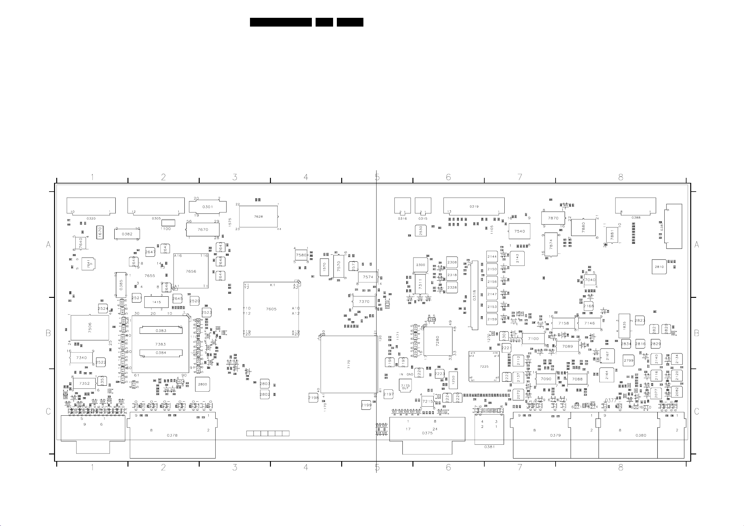
Electrical Diagrams and PWB Layouts
Layout SCAVIO Panel (Overview Top Side)
0301 A3
0305 A2
0315 A6
0316 A5
0318 A6
0319 A6
0320 A1
0375 C6
0376 C1
0378 C2
0379 C7
0380 C8
0381 C7
0382 A1
0383 B2
0384 B2
0385 A1
0387 A8
0388 A8
1100 A2
1105 A7
1170 C4
1171 B5
1250 C6
1270 B7
1415 B2
1570 A4
1575 A3
1670 A1
1835 B8
2002 C8
2003 C8
2004 C8
2005 C8
2008 C8
2012 C8
2014 C8
2015 C8
2021 C8
2030 C8
2040 A8
2041 A8
2042 A8
2060 A7
2072 C7
2077 C8
2082 C8
2088 C8
2089 B7
2090 C7
2097 C8
2103 C7
2105 B7
2106 B7
2107 B7
2108 B7
2109 B7
2110 B7
2111 B8
2112 B7
2113 B7
2114 C8
2115 C7
2116 C8
2117 C8
2118 C7
2119 C6
2120 C8
2123 C7
2124 C7
2127 B8
2128 B7
2134 B8
2137 C7
2140 B8
2142 A7
2143 A7
2144 A7
2145 B8
2146 B5
2147 A7
2150 A7
2151 B5
2152 B5
2153 B7
2156 A7
2157 B8
2158 B5
2159 B7
2161 C8
2164 C8
2165 C8
2166 B8
2167 B8
2168 B8
2195 B5
2196 B5
2197 C5
2198 C4
2199 C5
2217 C6
2220 C6
2221 B7
2222 C7
2223 C6
2224 C6
2225 A8
2226 A8
2228 C6
2252 C6
2253 C6
2254 C6
2260 C6
2261 C6
2262 C6
2263 C6
2264 C6
2265 C7
2266 C6
2267 C6
2268 C7
2269 C7
2270 C7
2274 C7
2275 C7
2276 C7
2277 C7
2278 C7
2279 C7
2300 A6
2301 A6
2302 B7
2308 A6
2311 A6
2318 A6
2328 A6
2335 B5
2336 C3
2337 B3
2338 C3
2340 B1
2343 C1
2351 C1
2352 C1
2353 C1
2354 C1
2355 C1
2365 C1
2370 A5
2372 B5
2375 B5
2376 B5
2383 B2
2433 B2
2435 B2
2437 B2
2438 B2
2446 B2
2447 C2
2499 B1
2520 B2
2521 B2
2522 B1
2523 B3
2524 B1
2530 A6
2541 A7
2543 A6
2544 A6
2557 A6
2558 A6
2559 A6
2560 A6
2562 A7
2563 A7
2564 A7
2565 A7
2566 A6
2570 A4
2572 A4
2573 A5
2574 A5
2583 A4
2628 A3
2640 A1
2641 A1
2642 A2
2643 A3
2644 A3
2645 B2
2646 A2
2647 A2
2648 A3
2649 A2
2657 A3
2662 A3
2663 A3
2799 B8
2800 C3
2802 C3
2803 C3
2810 A8
2816 B8
2820 B8
2821 B8
2823 B8
2829 B8
2831 B8
2834 B8
2870 A8
2874 A7
2879 A8
2881 A8
3001 C8
3002 C8
3003 C8
3004 C8
3005 C8
3006 C8
3008 C8
3009 B3
3010 C8
3011 C8
3012 C8
3013 C8
3014 C8
3015 C8
3016 A5
3040 A8
3041 A8
3042 A8
3043 A8
3044 A8
3045 A8
3050 A8
3051 A8
3071 C8
3072 C7
3073 C7
3074 C7
3075 C7
3076 C8
3077 C8
3078 C8
3079 C8
3080 C8
3081 C8
3082 C8
3083 C8
3084 C8
3085 C8
3086 B8
3087 C8
3088 C8
3089 C8
3090 B7
3091 C7
3092 C8
3093 C7
3094 B8
3095 C8
3096 C8
3097 B8
3098 B8
3099 B7
3100 C8
3101 C7
3102 B7
3103 B7
3104 B8
3105 B8
3106 C8
3107 C8
3108 B7
3109 B7
3110 C8
3111 C7
3112 C7
3113 B7
3114 B8
3115 B7
3116 C8
3117 B8
3118 C8
3119 C8
3120 C8
3121 B8
3122 B7
3123 C8
3124 C7
3125 C8
3126 B8
3127 B8
3128 B8
3129 B8
3130 B8
3131 B7
3133 B5
3134 B8
3135 B8
3136 B8
3137 C7
3138 C7
3139 C7
3140 B8
3141 B8
3142 B8
3144 A6
3145 A7
3146 A7
3147 A6
3148 B7
3149 A7
3150 A6
3151 A7
3152 A7
3153 B6
3154 B7
3155 B7
3156 A6
3157 A7
3158 A7
3159 B6
3160 B7
3161 B7
3162 B5
3163 B8
3164 C8
3165 B7
3166 B5
3170 A6
3171 A6
3172 A6
3173 B7
3174 B7
3175 B7
3176 B7
3177 B7
3178 B8
3179 B7
3180 B8
3181 B8
3182 B8
3183 B7
3184 B7
3186 B7
3188 B7
3189 B8
3193 C7
3194 C6
3195 C7
3200 B5
3203 B5
3204 B5
3205 B5
3209 C5
3210 C5
3213 C6
3214 C6
3215 C6
3216 C6
3217 C6
3218 C6
3219 B5
3220 A8
3250 B7
3251 B7
3260 B7
3261 C6
3262 B7
3263 B7
3271 B7
3274 C8
3275 C6
3276 C7
3277 C8
3278 C7
3279 C7
55FM242 AB 7.
3284 B6
3285 B6
3286 B6
3289 B6
3290 B6
3291 B6
3292 B6
3293 B6
3297 B6
3298 B5
3299 B6
3304 B6
3305 B3
3306 A5
3308 A6
3309 A6
3310 A6
3311 A6
3316 A5
3318 A6
3319 A6
3320 A6
3321 A6
3323 A5
3324 A5
3328 A6
3329 A6
3330 A6
3331 A6
3333 A5
3334 A5
3336 B3
3337 B3
3338 B3
3339 B3
3340 B1
3346 B1
3351 B6
3352 C1
3353 C1
3354 C1
3355 C1
3359 A6
3363 C3
3364 C1
3365 C1
3366 C1
3370 A5
3371 A5
3373 A5
3374 A5
3375 B5
3376 B5
3377 B5
3378 B5
3379 B5
3380 B2
3381 B2
3382 B2
3383 B2
3385 B3
3386 B3
3387 B3
3389 B3
3390 B3
3391 B3
3392 B3
3393 B3
3394 B3
3397 B3
3398 B2
3401 B2
3402 C2
3404 C2
3406 C2
3410 C2
3413 C2
3414 C2
3415 C2
3424 C2
3425 C2
3426 C2
3427 C2
3428 C2
3429 C2
3448 B1
3449 B1
3451 B1
3452 C1
3453 C1
3460 B1
3461 B1
3462 B1
3463 B1
3464 B1
3483 C2
3484 C2
3485 C2
3486 C2
3487 C2
3488 C2
3489 C2
3496 B3
3502 B1
3503 B1
3506 B1
3510 B3
3512 B3
3519 B3
3520 B3
3536 A5
3540 A7
3541 A7
3542 A7
3543 A7
3544 A7
3545 A6
3546 A7
3547 A7
3556 A1
3557 A6
3558 A6
3559 A6
3560 A6
3570 A1
3571 A4
3572 A6
3573 A6
3575 A4
3578 C1
3580 A4
3581 A4
3582 A4
3583 A4
3610 B3
3611 A4
3625 A3
3626 A3
3627 A3
3640 A1
3641 A1
3655 A2
3657 A3
3658 A3
3660 B8
3667 B6
3668 B6
3679 A3
3687 B3
3710 C3
3720 C2
3730 C2
3740 C2
3750 C2
3760 C2
3809 C3
3810 A8
3811 A8
3814 A8
3836 C4
3837 C4
3879 A8
3880 A8
3900 C3
3905 A6
3906 A6
3907 A6
3909 A5
3913 C1
3914 A1
3915 B1
3918 B5
3919 A5
3920 A5
3922 B1
3924 C1
3925 C1
3926 C1
3927 C1
3928 C1
4008 A1
4011 A1
4146 B8
4152 B8
4158 B7
4200 B5
4201 B5
4202 B5
4203 B5
4215 C6
4216 C6
4220 C8
4381 B3
4500 C1
4572 A5
4574 A5
4654 A2
4659 A2
4710 C3
4720 C2
4730 C2
4740 C2
4750 C2
4760 C2
4770 C8
4774 C7
4778 C7
4782 C7
4786 C8
4790 C8
4871 A8
4872 A8
4873 A8
4874 A8
4875 A8
4876 A8
4890 A8
4891 A8
4892 A8
4893 A8
4894 A8
4895 A8
4896 A8
4897 A8
4898 A1
5089 B8
5090 B8
5140 A7
5161 C8
5164 C8
5166 B8
5167 B8
5170 C8
5175 B7
5180 B7
5196 B5
5197 B5
5198 C4
5199 C5
5210 C6
5214 C6
5221 B7
5222 C7
5223 C6
5224 C6
5226 C6
5228 B5
5300 A6
5302 B7
5350 C1
5352 C1
5520 A2
5524 B1
5541 A7
5570 A4
5572 A5
5574 A5
5628 A3
5642 A2
5643 A3
5644 A3
5646 A2
5647 A2
5648 A3
5649 A2
5810 A8
5820 B8
5834 B8
5870 A7
6001 C8
6010 C8
6071 C8
6076 C8
6091 C8
6105 B7
6166 B8
6200 C5
6201 C5
6202 C6
6203 C6
6204 C5
6205 C5
6206 C5
6207 C5
6208 C5
6209 C5
6210 C6
6214 C6
6274 C8
6276 C6
6277 C6
6278 C7
6302 B7
6315 C1
6316 C1
6317 C1
6318 C1
6319 C1
6320 C1
6321 C1
6322 C1
6323 C1
6324 C1
6353 C1
6354 C1
6355 C1
6356 C1
6357 C1
6365 C1
6366 C1
6378 B5
6379 B5
6388 B3
6393 B3
6399 B3
6508 B3
6509 B3
6551 C1
6552 C1
6553 C1
6554 C1
6555 C1
6556 C1
6710 C3
6711 C3
6720 C2
6721 C2
6730 C2
6731 C2
6740 C2
6741 C2
6750 C2
6751 C2
6760 C2
6761 C2
6770 C8
6771 C8
6774 C7
6775 C7
6778 C7
6779 C7
6782 C7
6783 C7
6786 C8
6787 C8
6790 C8
6791 C8
6820 B8
6821 B3
7006 C8
7010 C8
7040 A8
7041 A8
7074 C7
7075 C7
7079 C8
7080 C8
7084 C8
7085 C8
7088 C8
7089 B8
7090 C7
7100 B7
7102 B7
7103 B7
7104 B8
7105 B8
7107 B7
7110 B7
7111 B7
7112 B7
7113 B7
7115 B7
7117 C8
7121 C8
7129 B8
7130 B8
7131 B7
7135 B8
7138 C7
7141 B8
7145 A7
7146 B8
7148 A7
7151 A7
7154 B7
7157 A7
7158 B8
7160 B7
7165 B8
7170 B5
7175 C5
7215 C6
7225 B6
7280 B6
7308 A6
7309 B6
7311 A6
7318 A6
7319 B5
7320 B3
7321 B3
7322 B3
7323 C3
7328 A6
7333 B6
7340 B1
7352 C1
7364 C1
7370 B5
7383 B2
7432 C2
7433 C2
7506 B1
7540 A7
7570 A4
7574 A5
7580 A4
7605 B4
7628 A3
7640 A1
7641 A1
7655 A2
7656 A2
7670 A3
7870 A7
7874 A7
7879 A8
7880 A8
7881 A8
Part 1
CL 36532051_29a.eps
Part 2
CL 36532051_29b.eps
3122 123 6001.7
CL 36532051_029.eps
040703
Page 56
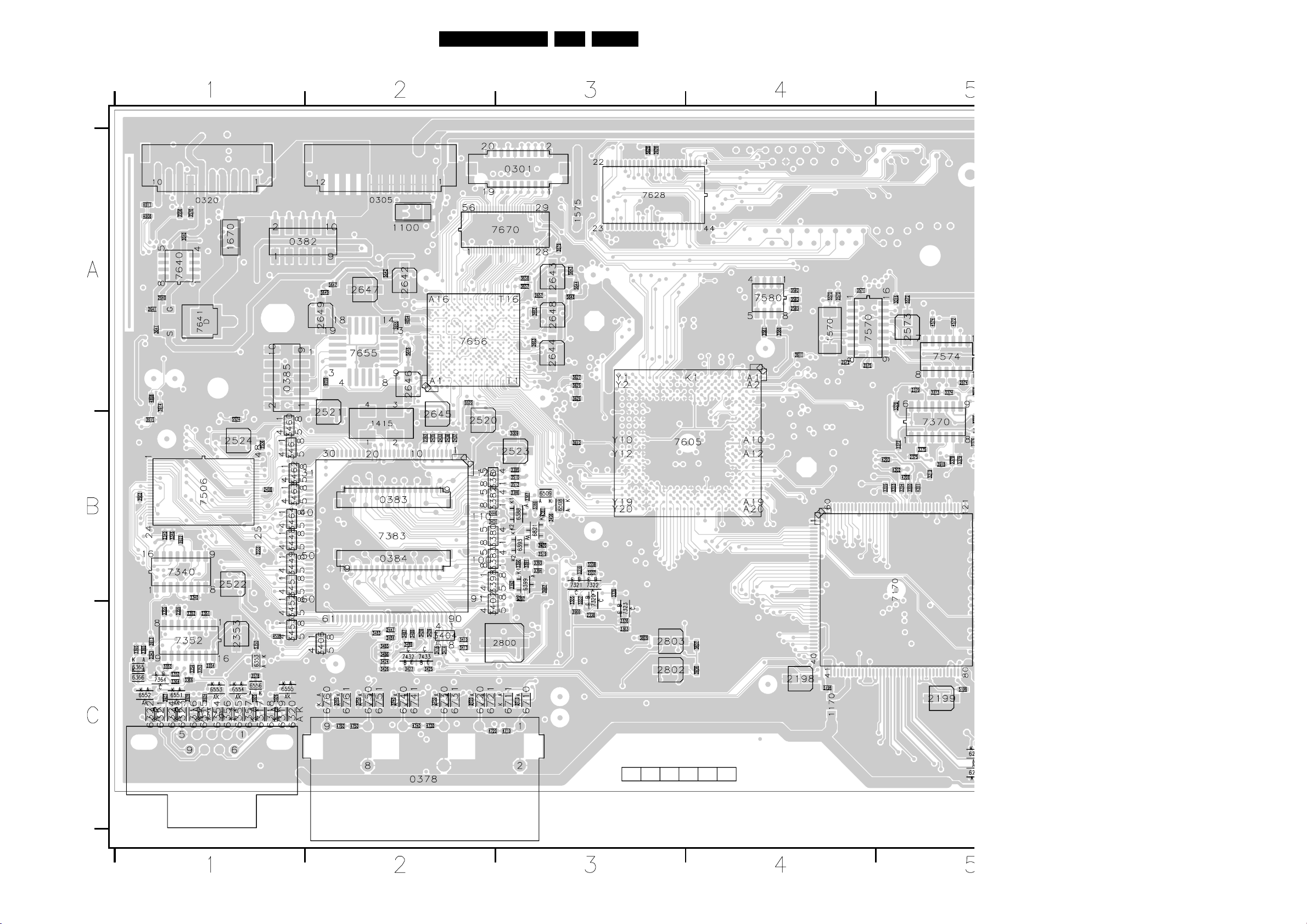
Electrical Diagrams and PWB Layouts
Layout SCAVIO Panel (Part 1 Top Side)
56FM242 AB 7.
CL 36532051_29a.eps
240603
Page 57
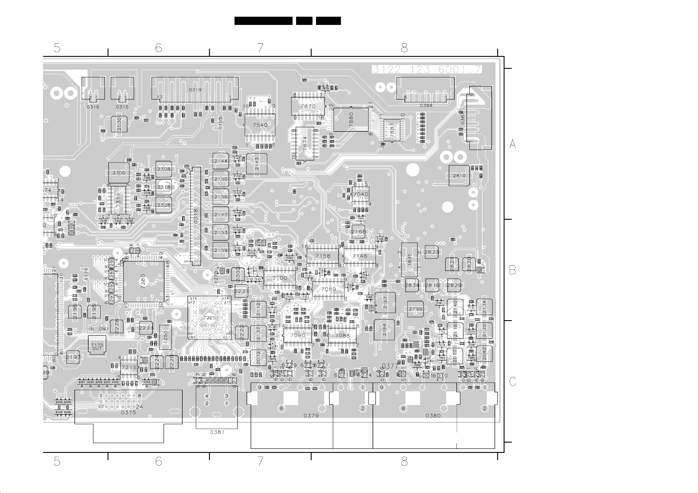
Electrical Diagrams and PWB Layouts
Layout SCAVIO Panel (Part 2 Top Side)
57FM242 AB 7.
CL 36532051_29b.eps
240603
Page 58
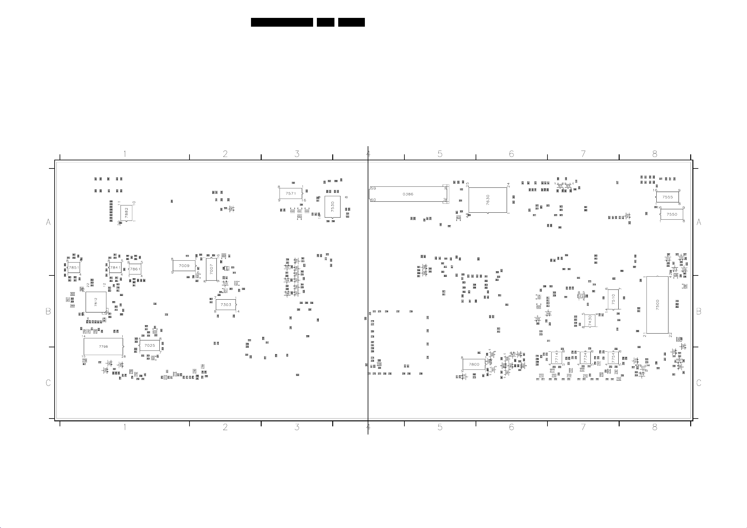
Electrical Diagrams and PWB Layouts
Layout SCAVIO Panel (Overview Bottom Side)
0386 A5
2000 C1
2001 C1
2007 A2
2009 B2
2020 B1
2022 B1
2034 C1
2061 B5
2066 A5
2160 B2
2162 B2
2170 C4
2171 C4
2172 C4
2173 C4
2174 B4
2175 B4
2176 B4
2177 B4
2178 B4
2179 C4
2180 C4
2181 B4
2182 C4
2183 C4
2184 C4
2185 C5
2186 B5
2187 B4
2188 B4
2189 C5
2190 C5
2191 B5
2192 B5
2193 B5
2205 B4
2206 B4
2207 B4
2208 C4
2209 C4
2210 C4
2211 C4
2212 B4
2230 C3
2231 C3
2232 C2
2240 B2
2247 B3
2248 B3
2249 B2
2250 B2
2280 B3
2281 B3
2282 B3
2283 B3
2284 B3
2285 B3
2286 B3
2287 B3
2288 B3
2304 B2
2305 B2
2306 B2
2310 B2
2341 A8
2345 A8
2356 C8
2381 B7
2382 B7
2415 B7
2416 B7
2418 B6
2419 B6
2420 B6
2432 B7
2434 B7
2436 B7
2439 B7
2448 B7
2500 B8
2501 B8
2502 B8
2503 B8
2504 B8
2505 B8
2506 B8
2511 B7
2513 B7
2515 C8
2531 A3
2533 A4
2534 A4
2535 A4
2537 A7
2538 A7
2546 A8
2547 A8
2548 A8
2550 A8
2551 A8
2552 A8
2553 A8
2554 A8
2555 A8
2581 A3
2584 A3
2600 B6
2601 B6
2602 B6
2603 B6
2604 B6
2605 B6
2606 B5
2607 B5
2608 B5
2609 B5
2610 B5
2611 B5
2612 B6
2613 B6
2614 B6
2615 A5
2616 B6
2617 B5
2618 B6
2619 B5
2620 B6
2621 B5
2622 B6
2623 A6
2624 B6
2625 B6
2629 A5
2630 A5
2655 A7
2656 A7
2658 A7
2659 A7
2660 A7
2661 A7
2666 A7
2670 A7
2671 A6
2672 A6
2673 A7
2674 A6
2694 A6
2695 A6
2696 A6
2697 A6
2698 A6
2699 A7
2711 C6
2712 C6
2714 C6
2715 C7
2716 C6
2717 C7
2721 C7
2722 C7
2724 C7
2726 C7
2727 C7
2731 C7
2732 C7
2734 C7
2735 C7
2736 C7
2737 C7
2741 C7
2742 C7
2744 C7
2746 C7
2747 C7
2751 C7
2752 C7
2754 C7
2755 C7
2756 C7
2757 C7
2761 C7
2762 C7
2764 C8
2766 C8
2767 C7
2771 C1
2772 C1
2775 C1
2776 C1
2779 C2
2780 C2
2783 C2
2784 C2
2787 C1
2788 C1
2791 C1
2792 C1
2794 B1
2795 B1
2796 C1
2797 B1
2798 B1
2801 C6
2804 C6
2811 B1
2812 B1
2813 B1
2814 B1
2815 B1
2817 B1
2818 B1
2819 B1
2822 B1
2824 B1
2825 B1
2826 B1
2827 B1
2828 B1
2830 B1
2833 B1
2835 B1
2836 B1
2837 B1
2838 B1
2839 B1
2840 A1
2841 B1
2842 A1
2843 B1
2844 A1
2845 B1
2846 A1
2848 A1
2849 A1
2850 A1
2851 B1
2852 A1
2853 B1
2854 A1
2856 A1
2857 A1
2858 A1
2859 B1
2861 A1
2862 B1
2863 B1
2864 A1
2865 A1
2867 A1
2868 B1
2869 B1
2880 A1
2882 A1
3000 C1
3007 B2
3018 B7
3019 A2
3020 B1
3021 B1
3022 B1
3023 B1
3024 B1
3025 C1
3026 C1
3030 B1
3031 C1
3032 C1
3033 C1
3034 C1
3035 B1
3036 B1
3052 A2
3053 A2
3054 A2
3060 A5
3061 A5
3065 A5
3066 A5
3132 B1
3190 B1
3206 C4
3207 C4
3208 C4
3211 C5
3212 C5
3225 C2
3294 A8
3295 A8
3296 B8
3300 A3
3301 A3
3302 B3
3303 B3
3307 A8
3312 A3
3313 A3
3314 A3
3315 A3
3317 A8
3322 A3
3325 A3
3326 A8
3327 A8
3332 A3
3335 B3
3341 C8
3342 C8
3343 C8
3344 C8
3345 C8
3347 C8
3348 A8
3349 B8
3350 C8
3356 A3
3357 A3
3358 A3
3360 C8
3361 C8
3362 C8
3367 B3
58FM242 AB 7.
3368 B3
3369 B3
3372 A8
3384 B7
3388 B6
3400 A8
3405 B6
3411 B7
3417 A8
3418 B7
3419 A8
3420 A7
3421 A7
3422 A7
3423 A8
3430 B7
3431 B7
3432 B7
3433 B7
3435 B7
3436 B7
3450 B7
3490 B7
3494 B7
3507 B8
3511 B7
3513 B7
3514 C8
3515 C8
3516 C8
3517 C8
3518 C8
3530 A3
3531 A3
3532 A3
3533 A3
3534 A4
3535 A4
3537 A3
3538 A4
3539 A3
3548 A2
3549 A4
3550 A8
3551 A8
3552 A8
3553 A8
3554 A3
3555 A4
3561 A2
3562 A2
3563 A2
3564 A2
3565 A2
3566 A2
3567 A2
3568 A4
3569 A3
3577 A8
3590 A5
3591 A5
3592 A5
3593 A5
3594 A3
3600 A5
3601 A5
3602 A5
3603 A5
3604 A5
3605 A5
3606 B5
3607 A5
3608 B5
3609 A5
3612 B6
3613 B6
3615 B5
3616 A5
3617 A5
3620 A6
3621 B5
3622 B5
3623 B5
3628 A6
3630 A6
3631 A5
3632 A5
3633 A6
3634 A5
3636 A5
3637 A5
3638 A5
3639 A5
3653 A7
3654 A7
3661 A7
3662 A7
3663 A7
3664 A7
3665 A7
3666 A7
3670 A6
3671 A7
3672 A6
3673 A6
3674 A6
3675 A6
3676 A6
3677 A6
3681 A7
3682 A7
3685 A7
3686 A7
3688 A7
3689 A7
3711 C6
3713 C7
3714 C6
3716 C6
3717 C5
3718 C5
3719 C5
3721 C7
3723 C7
3724 C7
3726 C7
3731 C7
3733 C7
3734 C7
3736 C7
3741 C7
3743 C7
3744 C7
3746 C7
3751 C7
3753 C7
3754 C7
3756 C7
3761 C7
3763 C7
3764 C8
3766 C8
3771 C1
3772 C1
3773 C1
3775 C1
3776 C1
3777 C1
3779 C2
3780 C2
3781 C2
3783 C2
3784 C2
3785 C2
3787 C1
3788 C1
3789 C1
3791 C1
3792 C1
3793 C1
3794 B1
3795 B1
3796 C6
3797 C6
3798 C6
3800 C6
3801 C6
3802 C6
3803 C6
3804 C6
3805 C6
3806 C6
3807 C6
3808 C6
3812 B1
3813 B1
3815 B1
3816 B1
3817 C1
3818 B1
3820 C6
3821 C6
3822 C6
3835 B1
3840 A1
3841 B1
3843 B1
3844 A1
3845 A1
3846 A1
3847 A1
3848 B1
3849 A1
3850 A1
3851 B1
3853 B1
3854 A1
3855 A1
3856 A1
3857 A1
3858 B1
3859 A1
3860 B1
3861 B1
3862 B1
3863 A1
3864 A1
3865 A1
3866 B1
3867 B1
3870 A1
3901 A8
3902 A3
3903 A3
3904 B3
3908 B2
3910 A2
3911 B2
3912 B2
3917 B2
3921 C8
3923 B2
4006 A2
4007 A2
4009 B1
4010 A1
4250 C3
4315 A3
4316 A8
4325 B3
4335 B3
4385 B6
4430 B7
4431 B7
4505 B8
4506 B7
4581 A5
4582 A5
4591 A5
4592 A3
4593 A3
4605 B5
4632 A5
4655 A8
4656 A8
4657 A8
4658 A8
4680 A7
4684 A7
4794 B1
4797 C1
4800 C5
4801 C6
4810 B1
4811 B1
4882 A1
4883 A1
4884 A1
4885 A1
4886 A1
4887 A1
4888 A1
4889 A1
5000 C1
5007 A2
5009 A2
5020 B1
5060 A2
5160 B2
5162 B2
5220 C3
5521 B7
5522 C8
5523 B7
5530 A3
5630 A5
5645 B7
5670 A7
5672 A7
5673 A7
5796 C6
5798 B1
5822 B1
6007 B2
6009 A2
6019 A2
6022 B1
6034 C1
6310 B2
6311 B2
6380 A8
6381 B8
6500 A3
6501 A3
6502 A3
6503 A3
6504 B6
6505 B6
6507 B8
6630 A5
6802 C6
6805 C6
6807 C6
7000 C1
7001 C1
7002 C1
7007 A2
7009 A1
7025 B1
7060 A5
7065 A5
7303 B2
7305 A3
7306 B3
7307 B3
7310 B2
7315 A8
7316 A8
7325 A8
7326 A8
7341 C8
7343 C8
7356 A3
7357 A3
7358 A3
7360 C8
7362 B8
7365 B3
7366 B3
7367 B3
7405 B6
7406 B7
7430 B7
7435 A8
7500 B8
7510 B7
7515 C8
7516 C8
7517 C8
7530 A3
7550 A8
7555 A8
7563 A2
7571 A3
7630 A6
7675 A7
7676 A7
7714 C7
7718 C5
7734 C7
7754 C7
7798 B1
7800 C5
7801 C6
7802 C6
7803 C6
7805 C6
7806 C6
7807 C6
7808 C6
7812 B1
7841 A1
7851 A1
7861 A1
7882 A1
Part 1
CL 36532051_30a.eps
Part 2
CL 36532051_30b.eps
3122 123 6001.7
CL 36532051_030.eps
040703
Page 59
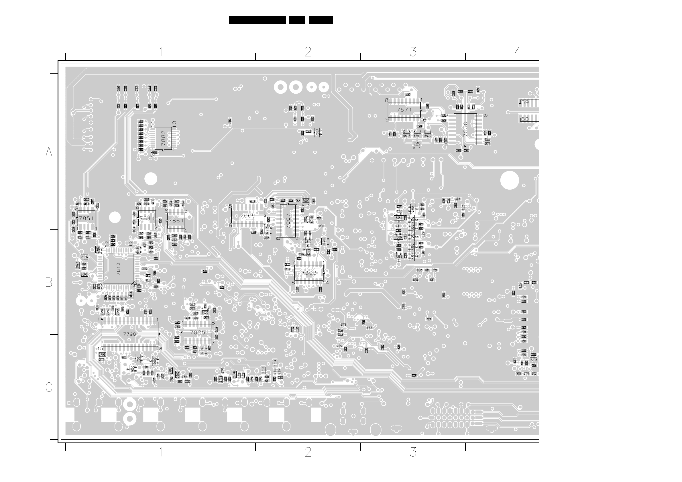
Electrical Diagrams and PWB Layouts
Layout SCAVIO Panel (Part 1 Bottom Side)
59FM242 AB 7.
CL 36532051_30a.eps
240603
Page 60
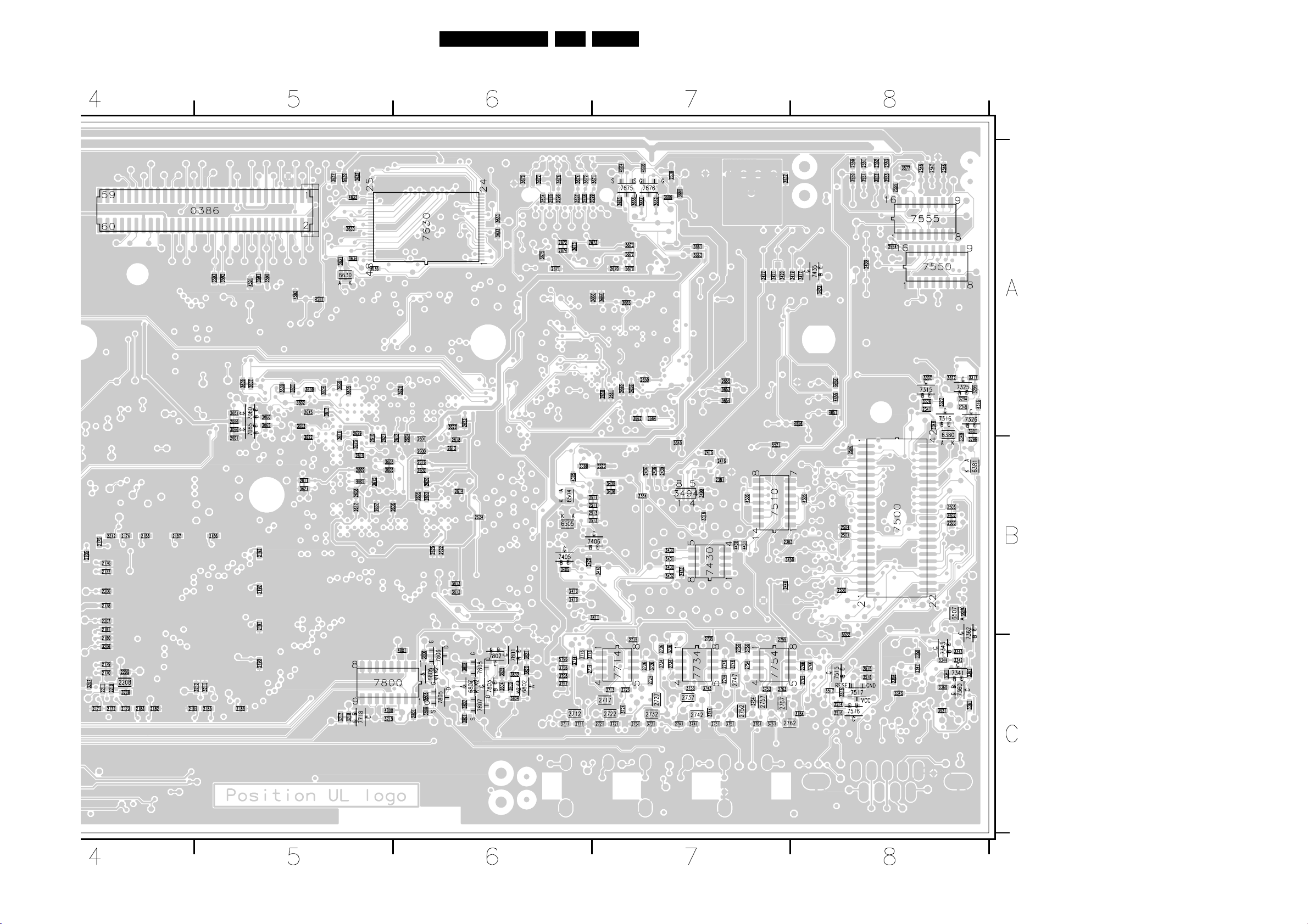
Electrical Diagrams and PWB Layouts
Layout SCAVIO Panel (Part 2 Bottom Side)
60FM242 AB 7.
CL 36532051_30b.eps
240603
Page 61
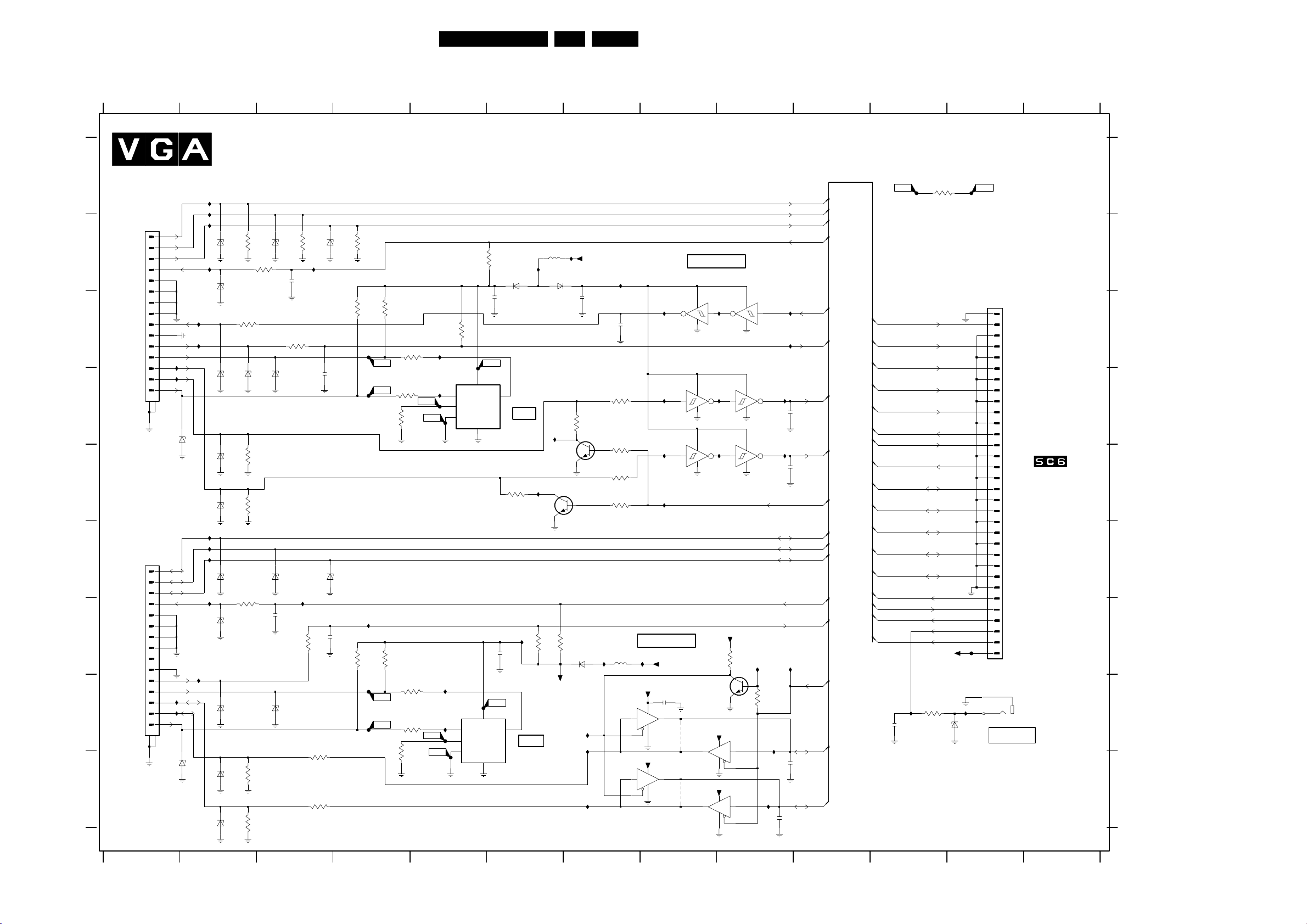
VGA Connector Panel
Electrical Diagrams and PWB Layouts
61FM242 AB 7.
12345678910111213
VGA CONNECTOR
A
I905
I906
6909
6921
I907
I908
I913
I914
DDC_SDA_1
DDC_SCL_1
BZM55-C33
I935
I936
I937
I938
I940
DDC_SDA_2
DDC_SCL_2
BZM55-C33
6900
6903
6906
6910
69116915
6912
6918
6922
6923
3900
BZM55-C33
BZM55-C33
3906
100R
6907
BZM55-C33
3912
BZM55-C33
3914
BZM55-C33
BZM55-C33
3915
100R
BZM55-C33
BZM55-C33
3923
BZM55-C33
3925
BZM55-C33
75R
6901
3903
100R
6908
BZM55-C33
1K
1K
6913
2907
6920
1K
1K
3901
BZM55-C33
100n
2900
3907
BZM55-C33
BZM55-C33
I939
RES
100n
BZM55-C33
I917
RES
100R
3916
75R
3922
100R
3924
100R
100R
2904
6902
6914
2908
BZM55-C33
RES
100n
BZM55-C33
RES
100n
3902
3904
3917
75R
10K
I943
10K
3905
3918
F911
F912
F941
F942
10K
10K
3909
100R
3910
3921
3908
100R
10K
3919
100R
3920
100R
10K
F914
I918
I919
F913
F944
7904
ST24FC21
7
3
I944
ST24FC21
I945
F943
3927
4K7
3928
F915
8
VCC
SCL6SDA
NC1
VCLK
DU
NC2
VSS
4
7907
8
VCC
SCL6SDA
7
VCLK
3
DU
VSS
4
2901
F945
NC1
NC2
4K7
2909
BAT254
100n
5
1
2
100n
5
1
2
6904
NVM
3940
75R
RES
I954
I960
BC847BW
NVM
I920
3929
100MHZ
7940
RES
4K7
I931
5900
6905
BAT254
I933
7937
BC847BW
RES
3930
+5V
2902
3937
4K7
6916
BAT254
I956
I947
I948
+5V_STBY_SW
100n
3911
100R
75R
RES
3913
100R
I946
100MHZ
74HCT125D
74HCT125D
I921
2903
3938
4K7
RES
3939
4K7
RES
5901
7910-A
RES
100n
4 x BUFFER
I955
+5V
14
2
7
1
7910-C
+5V
14
9
7
10
4 x BUFFER
14
I922
7
7900-F
74HCT14D
I923
13 12
7900-A
74HCT14D
I924
12
I962
+5V_STBY_SW
2910
100n
3
4910
8
4911
7900-C
74HCT14D
56
14
7
14
7
BC847BW
14
6
14
11
I932
74HCT14D
I926
74HCT14D
I927
7915
+5V
7
+5V
7
7900-D
74HCT14D
14
98
7
7900-E
14
11 10
7
7900-B
14
34
7
+5V
10K
3934
I957
33K
3935
7910-B
74HCT125D
5
4
7910-D
74HCT125D
12
13
I949
I950
0371
748390
1
2
B
VGA1
C
IN
D
3
4
5
6
7
8
9
10
11
12
I915
13
I916
14
15
1617
E
F
VGA2
G
IN / OUT
H
0372
748390
1
2
3
4
5
6
7
8
9
10
11
12
I941
13
I942
14
15
1617
I
I929
I930
I925
2905
I928
2906
EBOX_PRESENT
I958
2911
100n
2912
VGA1_TXD
RC_VGA1
VGA1_RXD
RES
100n
RES
100n
VGA2_TXD
VGA2_RXD
VGA_OUTN
VGA2_V
RES
100n
VGA2_H
RES
VGA1_R
VGA1_G
VGA1_B
VGA1_V
VGA1_H
VGA2_R
VGA2_G
VGA2_B
F905
VGA1_R
VGA1_G
VGA1_B
VGA1_H
VGA1_V
VGA1_TXD
VGA1_RXD
RC_VGA1
VGA2_R
VGA2_G
VGA2_B
VGA2_H
VGA2_V
VGA2_TXD
VGA2_RXD
EBOX_PRESENT
VGA_OUTN
I952
100n
2925
+5V_STBY_SW
3926
100R
RES
3999
RES
RC_OUT
F900
I951
6925
BZM55-C33
F906
0318
1
2
3
4
5
6
7
8
9
10
11
12
13
14
15
16
17
18
19
20
21
22
23
24
25
26
27
28
29
30
31
32
YKB11-0482
1
2
0374
RC-OUT
TO
0318
SCAVIO
CL 26532038_052.eps
150402
0318 C13
0371 B1
0372 F1
0374 H13
2900 B3
2901 C6
2902 C7
2903 C7
2904 D3
2905 D9
2906 E9
2907 G3
A
2908 G3
2909 G6
2910 H8
2911 I9
2912 I9
2925 H11
3900 B2
3901 B3
3902 B4
3903 B3
3904 C4
3905 C4
B
3906 C2
3907 C3
3908 C5
3909 D5
3910 D5
3911 D7
3912 E2
3913 E7
3914 E2
3915 G2
3916 G3
3917 G4
C
3918 G4
3919 H5
3920 H5
3921 I5
3922 I3
3923 I2
3924 I3
3925 I2
3926 H12
3927 B5
3928 C5
D
3929 G6
3930 G6
3934 G9
3935 H9
3937 D6
3938 E7
3939 E7
3940 E6
3999 A12
4910 H8
4911 I8
5900 B6
E
5901 G7
6900 B2
6901 B3
6902 B3
6903 B2
6904 B6
6905 B6
6906 D2
6907 D2
6908 D3
6909 D1
6910 E2
F
6911 E2
6912 F2
6913 F3
6914 F3
6915 G2
6916 G7
6918 H2
6920 H3
6921 I1
6922 I2
6923 I2
G
6925 H12
7900-A D8
7900-B D9
7900-C C8
7900-D C9
7900-E D9
7900-F D8
7904 D5
7907 H5
7910-A H7
7910-B H9
7910-C I7
H
7910-D I9
7915 H9
7937 E6
7940 E6
F900 G12
F905 A11
F906 A12
F911 C4
F912 D4
F913 D5
F914 D5
F915 D5
I
F941 H4
F942 H4
F943 H5
F944 I5
F945 H5
I905 A2
I906 A2
I907 B2
I908 B2
I913 C2
I914 C2
I915 C1
I916 D1
I917 B3
I918 C5
I919 D5
I920 B6
I921 B7
I922 C8
I923 D8
I924 E8
I925 D9
I926 D9
I927 E9
I928 E9
I929 C9
I930 C9
I931 B7
I932 C9
I933 D6
I935 F2
I936 F2
I937 F2
I938 G2
I939 G3
I940 H2
I941 H1
I942 H1
I943 G4
I944 H5
I945 H5
I946 G7
I947 H6
I948 I6
I949 H9
I950 I9
I951 H12
I952 H12
I954 G6
I955 G8
I956 H7
I957 G9
I958 G9
I960 E6
I962 E8
12345
6789
10 11 12
13
Page 62
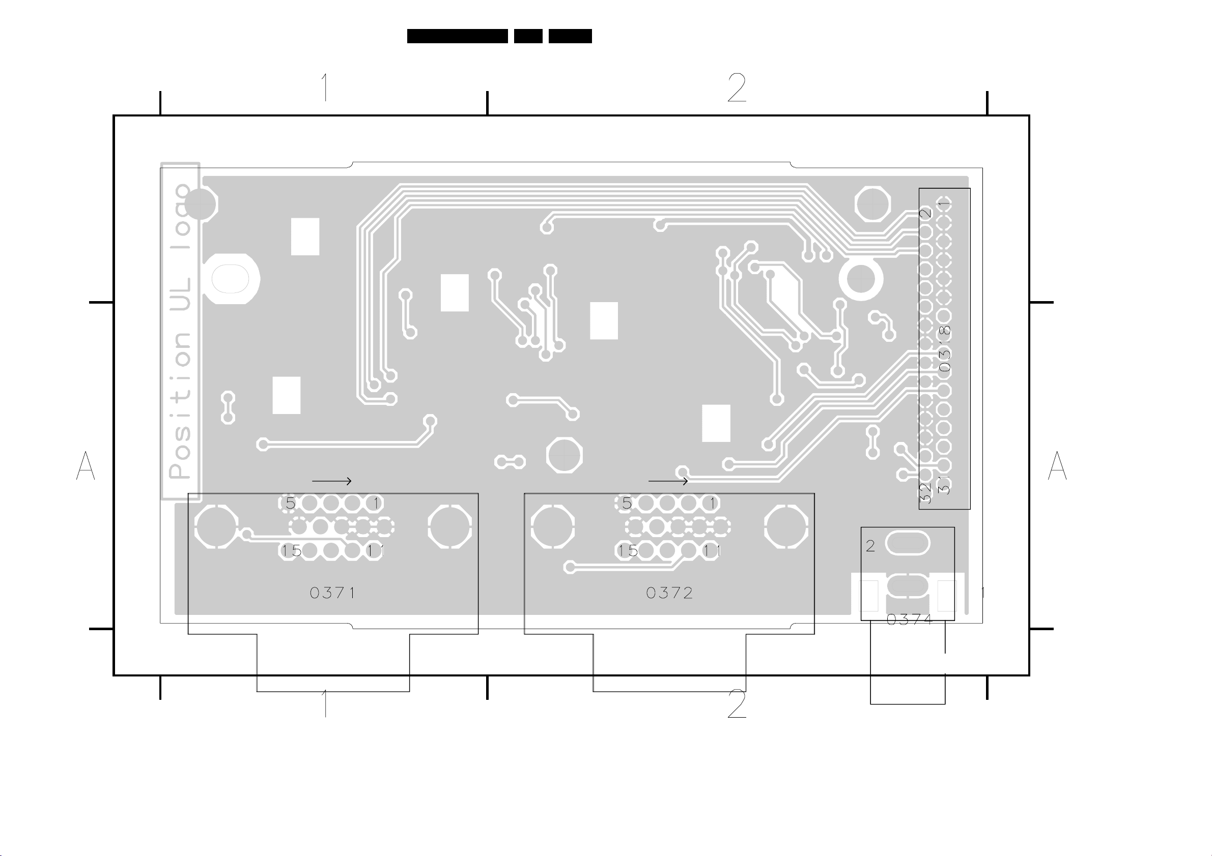
Electrical Diagrams and PWB Layouts
Layout VGA Connector Panel (Top Side)
62FM242 AB 7.
0318 A2
0371 A1
0372 A2
0374 A2
CL 26532038_053.eps
150402
Page 63
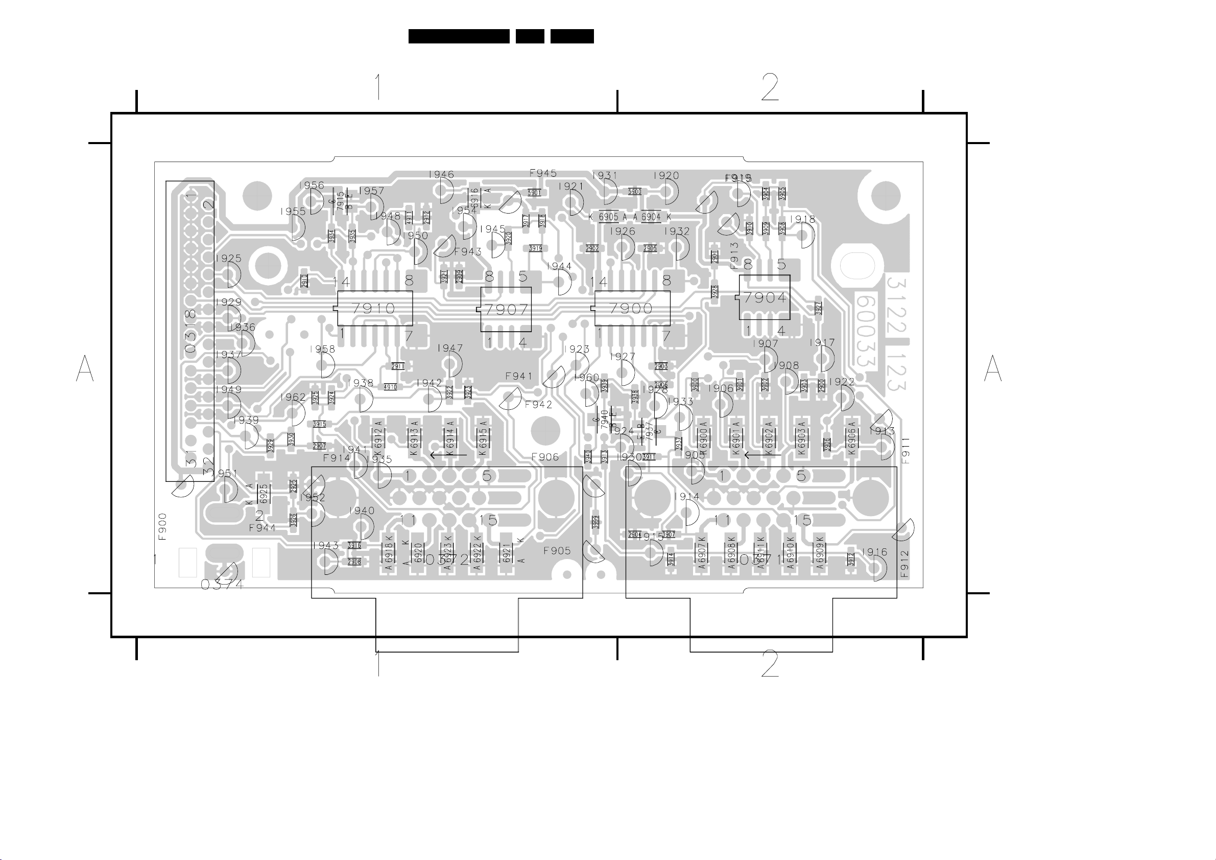
Electrical Diagrams and PWB Layouts
Layout VGA Connector Panel (Bottom Side)
63FM242 AB 7.
CL 26532038_053.eps
150402
0318 A1
0371 A2
0372 A1
0374 A1
2900 A2
2901 A2
2902 A1
2903 A2
2904 A2
2905 A2
2906 A2
2907 A1
2908 A1
2909 A1
2910 A1
2911 A1
2912 A1
2925 A1
3900 A2
3901 A2
3902 A2
3903 A2
3904 A2
3905 A2
3906 A2
3907 A2
3908 A2
3909 A2
3910 A2
3911 A2
3912 A2
3913 A1
3914 A2
3915 A1
3916 A1
3917 A1
3918 A1
3919 A1
3920 A1
3921 A1
3922 A1
3923 A1
3924 A1
3925 A1
3926 A1
3927 A2
3928 A2
3929 A1
3930 A1
3934 A1
3935 A1
3937 A2
3938 A2
3939 A1
3940 A1
3999 A1
4910 A1
4911 A1
5900 A2
5901 A1
6900 A2
6901 A2
6902 A2
6903 A2
6904 A2
6905 A1
6906 A2
6907 A2
6908 A2
6909 A2
6910 A2
6911 A2
6912 A1
6913 A1
6914 A1
6915 A1
6916 A1
6918 A1
6920 A1
6921 A1
6922 A1
6923 A1
6925 A1
7900 A2
7904 A2
7907 A1
7910 A1
7915 A1
7937 A2
7940 A1
Page 64
Electrical Diagrams and PWB Layouts
64FM242 AB 7.
Personal Notes: Personal Notes:
Page 65
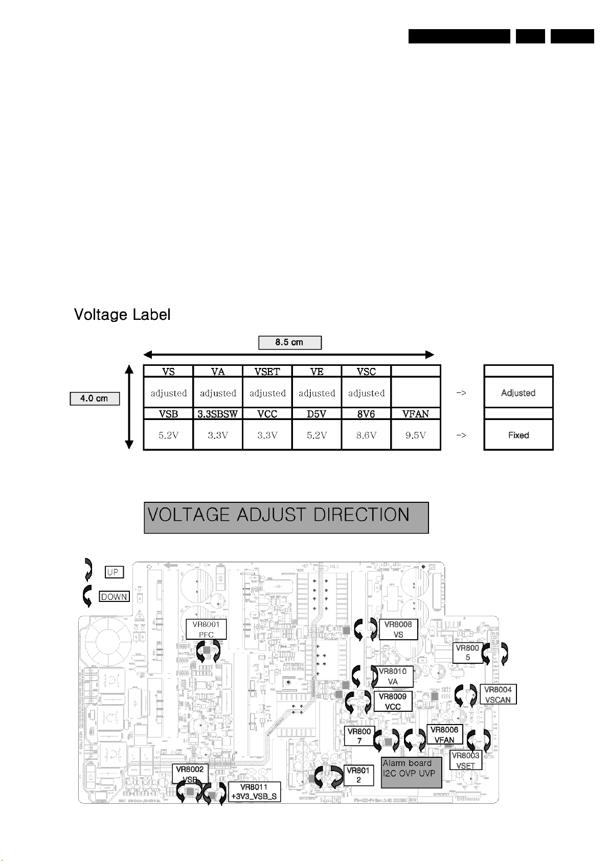
8. Alignments
Alignments
EN 65FM242 AB 8.
Index of this chapter:
1. General Alignment Conditions
2. Hardware Alignments
3. Software Alignments and Settings
Note: The Service Default Mode (SDM) and Service Alignment
Mode (SAM) are described in chapter “Service Modes”.
Menu navigation is done with the "CURSOR UP, DOWN, LEFT
or RIGHT" keys of the remote control transmitter.
8.1 General Alignment Conditions
Perform all electrical adjustments under the following
conditions:
• Mains voltage and frequency: 220 V
otherwise stated.
• Connect the set to the Mains via an isolation transformer.
• Allow the set to warm up for approximately 20 minutes.
• Measure the voltages and waveforms in relation to chassis
ground (with the exception of the voltages on the primary
/ 50 Hz unless
AC
side of the power supply). Never use the cooling fins/plates
as ground.
• Test probe: Ri > 10 MΩ, Ci < 2.5 pF.
• Use an isolated trimmer/screwdriver to perform the
alignments.
Use a VGA-generator or a Personal Computer (contact your
National Service Organisation for the necessary test pattern
files) as test pattern generator and connect it to the VGA1 input
of the FM242 plasma monitor. When you use a PC, start
Microsoft PowerPoint (or Paintbrush), and load the mentioned
file. Then display the picture as full screen.
8.2 Hardware Alignments
There no alignments needed, except in care the pdp has been
exchanged or the pdp-supply has been exchanged.
In that case the both must be matched.
Figure 8-1 Supply Alignment
Page 66
EN 66 FM242 AB8.
Alignments
Procedure:
• See figure above
• The 6 pot meters influencing VSB, 3.3SBSW, VCC, D5V,
8V6, VFAN are not critical for matching. In case of doubt
values can be checked versus mentioned voltages.
• The 5 pot meters VS, VA, VSET, VE, VSC have to be
matched with the values displayed on the pdp-label.
• Start with aligning pot meter VR8008 to adjust VS and then
respectively VR8010 (VA), VR8003 (VSET), VR8005 (VE),
VR8004 (VSCAN)
• To double check, repeat whole sequence again, to check
right value
8.3 Software Alignments
Enter the Service Alignment Mode (see chapter 5). The SAM
menu will now appear on the screen.
Select one of the following alignment menus via the upper
horizontal bar:
1. Scaler (Scal.)
2. Video 1 (Vid.1)
3. Video 2 (Vid.2)
4. Options (Opt.)
Note: the last three items are not available in the Basic
configuration.
8.3.1 General
Table 8-1 SAM Menu "Gen."
Service Alignment Menu General
Type nr. - AG Code 42FD9945/01 **00 00
SW version OTC AAAAAB-X.Y xxxxx
SW version PW AAAABC-X.Y xxxxx
SW version EPLD AAAABC-X.Y xxxxx
Errors 1 xx xx xx xx xx
Errors 2 xx xx xx xx xx
Operational hours xx
Reset error buffer Press OK to reset
Store Press OK to store
Store
Select this item, and press OK, to store the made alignments.
Note: There are several methods to exit the SAM, each with its
own characteristics:
• Switch the set "off" (with the Mains switch or by pulling the
Mains cord); new alignment settings are always stored,
even when item "store" was not activated!
• Switch the set to "Standby" by pressing the power button
on the remote control transmitter; new alignment settings
are always stored, even when item "store" was not
activated!
• Use a standard RC-transmitter and key in the code 00; new
alignment settings are not stored, except when item "store"
was activated!
8.3.2 Scaler
Table 8-2 SAM Menu "Scal."
Service Alignment Menu Scaler
Test pattern On / Off
Color temperature 6500K / 8700K / 10000K
White point Adjust ...
Align ADC Press OK to execute
Clear user settings Press OK to clear
The lower 2 menu lines, only are valid when having a VGAsource. (otherwise low lighted)
Test pattern
This function makes it possible to generate a "colour bar" test
pattern (generated by the PW Scaler IC). You can use this
picture, to check the video path, starting at the PW Scaler IC to
the plasma display.
Colour temperature
Select the appropriate colour temperature for the alignments
(see also "White point" adjustment below).
White Point
Table 8-3 SAM Menu "Scaler - White Point"
Service Alignment Menu Scaler - White point
White point red <-------------|------------> 125
White point green <---------|----------------> 100
White point blue <-----------|--------------> 110
Press OK when done
Method 1 (with colour analyser)
1. Supply, via an external VGA source (e.g. a PC with
1024x768 mode, or a VGA generator), a "White Drive" test
pattern (ask your NSO). This picture consists of a black
picture with in the middle a 100% white square.
2. Set BRIGHTNESS to "53" and CONTRAST to "65" (via the
standard customer menu).
3. Go to the SAM menu.
4. Set COLOUR TEMPERATURE to "8700 K".
5. Measure with a CTV colour analyser (calibrated with the
spectra) on the centre of the white square on the screen.
6. Select "White point" in the SAM Scaler menu, and press
CURSOR RIGHT.
7. Adjust with the CURSOR UP/DOWN or LEFT/RIGHT
command, the three white points Red, Green and Blue to
"128" (do not go above this value!), and align with one or
two of the drivers to the correct coordinates (see table).
8. Repeat the same measurement for respectively colour
temperature "6500 K" and "10000 K".
9. Repeat again if necessary.
Table 8-4 White Point XY-coordinates
Colour Temperature x y
5600 K (Cool) 313 329
8700 K (Normal) 289 299
10000 K (Warm) 280 289
Method 2 (without colour analyser)
Without a CTV colour analyser, it is possible to set some
parameters, which are based on average values from
production.
These values will be communicated in a later stage.
Table 8-5 White point RGB-values
Colour Temperature R G B
5600 K (Cool)
8700 K (Normal)
10000 K (Warm)
Align ADC
1. Supply, via an external VGA source (e.g. a PC, mode
1024x768), the "ADC alignment" test pattern (retrieve this
file of the NSO). This picture consists of a half black and
Page 67
Alignments
EN 67FM242 AB 8.
half white picture: black is 16, and white is 235 on a full
scale of 255 (=770 mV).
2. Go to the SAM menu.
3. Select "Align ADC" in the SAM Scaler menu, and press
CURSOR RIGHT.
4. The alignment is performed automatically.
8.3.3 Video 1 (Enhanced version only)
Table 8-6 SAM Menu "Vid. 1"
Service Alignment Menu Video 1
Test pattern On / Off
Brightness 0 <-----------|---------- > 255
Contrast 0 <-----------|---------- > 255
Sharpness 0 <-----------|---------- > 255
Test pattern
This function makes it possible to generate a "full white" test
pattern (generated by the de-interlacer SDA9400, item 7280).
You can use this picture, to check the video path of the external
inputs AV1, 2 and 3, starting at item 7280
Note: The proper functioning of the Digital Video Decoder
SAA7118 is not tested!
Note: To generate the test pattern, it is necessary to feed a
signal to one of the AV-inputs. (if not the menu lines are low
lighted)
Brightness
This is the setting of IC7225 (SAA7118). Not necessary to
align, fixed value is:
• PAL/SECAM: 132
• NTSC: 139
Contrast
This is the setting of IC7225 (SAA7118). Not necessary to
align, fixed value is:
• PAL/SECAM: 139
• NTSC: 128
Lum. delay NTSC
Apply a NTSC colour bar/grey scale pattern as a test signal.
Adjust value until the transients of the colour and black & white
part of the test area are at the same position. Fixed value is 4.
8.3.5 Options (Enhanced version only)
Table 8-8 SAM Menu "Opt."
Service Alignment Menu Options
Vs/Va control
Display size
Virgin On / Off
ICONN control On / Off
Fan control
Virgin
Normally "off". When this option is set to "on", the display starts
with the language selection menu.
ICONN control
Normally "off". Set this option to "on" in case a so-called
"ICONN"-box (for Hotel TV) is connected to the display.
Caution: When this option is set to "on", without an ICONNBox connected to the monitor, one cannot control the monitor
anymore (because the RC connection is interrupted).
There are two ways to restore the remote control again:
• Connect pin 8 (IR_TX) to pin 9 (IR_RX) on the RS232
connector of the monitor (the easiest way to do this, is to
make a "dummy" connector with these pins connected, and
plug this into the monitor), or
• Set the set in the Service Alignment Mode (SAM) via
shorting jumpers 1 and 2 of connector 0382 on the
SCAVIO panel. After this you can enter the appropriate
menu to set "ICONN control" to "off" again.
Sharpness
Not necessary to align, fixed value is 6.
8.3.4 Video 2 (Enhanced version only)
Table 8-7 SAM Menu "Vid. 2"
Service Alignment Menu Video 2
Lum. delay PAL 0 <-----------|---------- > 7
Lum. delay SECAM 0 <-----------|---------- > 7
Lum. delay NTSC 0 <-----------|---------- > 7
With the "Luminance delays" alignment, you can place the
luminance information on the chrominance information (push
brightness onto the colour). Use a colour bar/grey scale pattern
as test signal.
These values are normally fixed.
Lum. delay PAL
Apply a PAL colour bar/grey scale pattern as a test signal.
Adjust value until the transients of the colour part and black and
white part of the test pattern are at the same position. Fixed
value is 4.
Lum. delay SECAM
Apply a SECAM colour bar/grey scale pattern as a test signal.
Adjust value until the transients of the colour part and black and
white part of the test pattern are at the same position. Fixed
value is 4.
Page 68
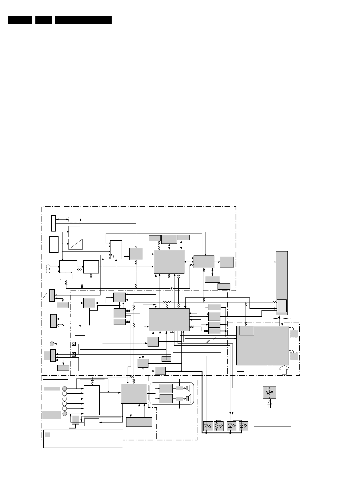
EN 68 FM242 AB9.
Circuit Descriptions and List of Abbreviations
9. Circuit Descriptions and List of Abbreviations
Index of this chapter:
1. General
2. Power Supply unit (very limited)
3. VGA connector panel
4. SCAVIO panel
5. Audio Amplifier panel
6. LED/Switch panel
7. Plasma Display Panel
8. Abbreviations
9. IC Block diagrams
Notes:
• Figures can deviate slightly from the actual situation, due
to different set executions.
• For a good understanding of the following circuit
descriptions, please use the diagrams in chapter 6 and 7.
Where necessary, you will find a separate drawing for
clarification.
9.1 General
The FM242 is the 3rd generation Philips plasma monitors.
Related to the FM242 it is a cost down product. A lower
specified pdp is used here (SDI-pdp), however performing still
very acceptable. In comparison to the FTV1.9DE, it has:
Video
DVI-D
AV3
AV2
AV1
Loop thru of RGB
and H,V s ignals
from VGA1 only
VGA2
RS232-C
VGA1
D
V
I
Y/G
Pb/B
Pr/R
H,V
1fH YUV
YC
CVBS
V
G
IN
A
OUT
2
RS
Sub-D
232
9 P
C
RC
out
V
G
In
A
1
Audio Processing
L/R VGA in
L/R CVBS
L/R YC
L/R HD
L/R DVI
L/R Flex VGA
(only output in
Basic config.)
! All Functional blocks shaded grey are r equired for
the"Basic Configuration".
The remainder is required f or the "Enhanced Configuration".
are optional or prepared
*
Y/H/V
YPbPr
Digital Video
Decoder
SAA7118
3D Comb*
NVM
DDC
R
S232C
ICONN
NVM
DDC
+9V_STBY
NVM
DDC
Sync
decoder
YPbPr
enable
audio
RGB
RGB+HV
RS232
Interrupt
gener.
RGB
RGB+HV
RGB+HV
De-interlacer
SDA9400
ST
RS 232
Driver
+5V_Stby_Sw
RS232C
activity int.
Contro l
Audio Switch
TEA6422D
Output
Switch
RGB+HV
H,V
RGB+HV
RS232C/
TTL
RC5 to E-box
Video +
switching
UART (Ebox)
TMDS
NVM
Flash ROM
32Kbit
UART
PW
Sync.
Interrupt
Gener.
Per channel
2Mbyte
PW
PixelWorks
PW164_10R or 10RK
Video Scaling
Co-processor
Interrupt
OTC
Main Pro cessor
SAA5801H/xx
SAM,
SDM,
RS232c
service
int. pins
UART
Interrupt
gener.
+9V_STBY
HP Filter +
Amp
LP Filter +
Amp
PW
Sync
select
PW/OTC
Switch
4052
IO Exp-
SC1
PCF8574
ADC Exp
PCF8591
H and/or V
from VGA1
I
RGB+HV
ADC +
TMDS
Decoder
AD9887
2
C_Bus -3
MSP Reset
MSP Audio Processor
MSP3415G
I2S
Audio D elay
32KSRAM
I2C_Bus 5
(sw bu s to NVM)
RGB+HV
Digital
YUV
Digital
UART
OTC
H,V
VGA1
switch-
VGA1
Switch
4052
CY7C1399
I2SI2S
Audio Amplifier
Figure 9-1 Control and Data Path
• The power supply has been exchanged by another supplypanel
• A new SCAVIO panel, which takes over the tasks of the
former AVC and LIMESCO panels.
• A new class-D audio amplifier,
• A VGA-resolution pdp. It is possible to use this product as
stand-alone monitor or, in combination with the so-called
F21R Receiver box, for TV applications.
There are two configurations:
• Basic: which has one video input (VGA1) and one video
output (VGA2). The VGA2 video output is directly
connected to the VGA1 video input, without any
processing. The audio output of VGA2 is also directly
connected to the VGA1 audio input.
• Enhanced: which has six video inputs (VGA1, VGA2, DVI-
D, CVBS, YC and HD) and six corresponding audio inputs.
These inputs are internally converted to the appropriate
signals. The VGA2 connection is here bi-directional (FlexVGA).
Note: In all descriptions below, the Enhanced version of the
FM242 is discussed. When there are important differences
between the Basic and Enhanced versions, this is mentioned.
SRAM
128kbyte
Reset
C_Bus -2
2
I
Mute
Mute
+9V_STBY
Tweeter
Low/Mid
video
control
(sw bus to NVM)
Fan Control PW M
Power OK, 5V test,
8V6 test
I2C_Bus 4
EPLD
EP1K30QC
IR RXr
(RC in)
PROM
for EPLD
Power ON
Reset
Flash
ROM
2Mbyte
DRAM
2Mbyte
NVM
32Kbit
generator
I2C_Bus -1
Light
Sensor
LVDS
Encoder
DS90C385
Clock
Red
LED
3v3Stby/
5vStdby
PDP go =>
<= IRQ_PDP
POWER_DOW N =>
PSU
Green
LED
Serial Digital RGB with
clock and Sync information
CPUgo =>
Display
Control
IO expander
PS
U
PCF8574AT
AC/DC, DC/DC converters
Audio supply, 5V,8V6, 3v3, Vs,Va
Protec tion
3v3,5v S tandby PSU
Fan driver
RC / LED / Switch Panel
PDP
MPU
Vs,Va,Vcc Vsago
PSU
ON/OFF switch
(see description)
CL 26532038_006.eps
AC i/p
2x
FAN
*
2x
FAN
010502
Page 69
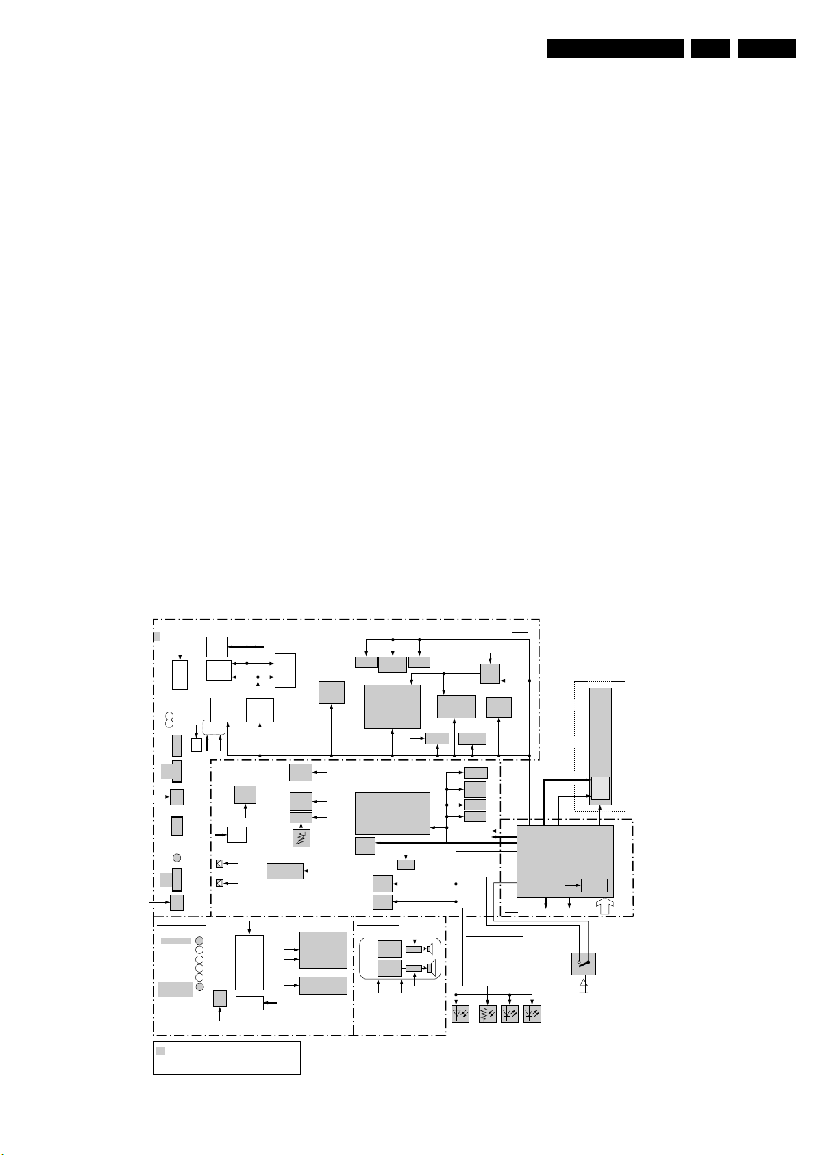
Circuit Descriptions and List of Abbreviations
EN 69FM242 AB 9.
9.1.1 Input/Output
The main inputs are:
• Basic: VGA only,
• Enhanced: VGA, Flex-VGA, DVI-D, HD-RGB+HV, HD-
2fH-YPbPr (sync on Y), 1fH-YCbCr (sync on Y), YC, CVBS
on cinch. Flex-VGA gives the user a choice to configure the
"loop-through VGA output" as an output or as input.
9.1.2 Video
This mainly consists of an analogue processing part and a
digital processing part. The video inputs like VGA (Basic
configuration), CVBS, YC, HD-RGB/YUV (1fH and 2fH) and
DVI-D are received and processed.
The VGA signals are first converted to digital signals and then
processed by the PW Scaler.
The YPbPr (2fH) signal is discretely converted to RGB,
whereas the YCbCr (1fH) signal is processed in the SAA7118
Digital Video decoder.
The base-band video inputs (CVBS and YC) are output from
this decoder as digital YUV, which are then further processed
by the Pixel Works Scaler (PW).
The signals on the digital DVI input are first decoded by the
TMDS decoder inside the AD9887 and then processed by the
PW Scaler.
The PW Scaler output is going through an EPLD and then via
an LVDS Encoder to the SDI PDP (Plasma Display Panel) as
differential serial data. This PDP has a resolution of 852(H) x
480 (V) pixels.
9.1.3 Audio
This mainly hosts the audio inputs for the various video inputs.
They go through an I
2
C controlled source selector. The main
audio processing is done by the Micronas MSP3415G version
with built-in UltraBass-II algorithm.
A digital delay line is created using the I
2
S channel and SRAM.
The delay created can be selected between two values, one for
the Receiver box, and one for the Monitor.
The processed audio signals are then differentially transmitted
to the audio amplifier panel. This amplifier drives a tweeter and
a twin-drive woofer (low/mid range). Active filtering is done
prior to the amplifiers.
9.1.4 Control
The main controller is the OTC, referred to as the "main
processor". This operates in co-ordination with the processor in
the Pixel Works Scaler (PW), referred to as the "co-processor".
When the FM242 monitor is connected to an F21R Receiver
box, the UART commands from the Receiver box will control
the monitor.
In stand-alone mode, the monitor can be controlled via the
Remote Control or via the RS232C port.
DDC1/2B (Digital Data Channel, an I
2
C-based protocol) is
implemented with separate identification NVMs for the two
VGA inputs and the DVI-D input as well. In addition, the
RS232C port can be used for software download to the PW and
the OTC. The target for downloading is controlled via a switch
in the RS232C path; the switch itself is controlled by the OTC.
9.1.5 Power Supply
Connectors
Y/G
Pb/B
Pr/R
AV3
H,V
YC
AV2
AV1
CVBS
D
V
DVI-D
I
Loop thru of RG
and H,V signals
from VGA1 only
V
B
G
Flex
A
2
NVM
DDC
+5V_STBY_SW
RS
Sub-D
232
9 P
C
RC
out
V
G
In
A
1
NVM
DDC
+5V_STB Y_SW
Audio processing Audio amplifier
L/R VGA in
L/R CVBS
L/R YC
L/R HD
L/R DVI
L/R Flex VGA
(only output in
Basic config.)
! All Functional blocks shaded grey are required f or
the"Basic Configuration".
The remainder is required for t he "Enhanced Configuration".
are optional or prepared
*
3D Comb*
+5V_STBY_SW
NVM
DDC
+5V
Sync
decode
YPbPr
+8V6
+5V
enable
+9V_STBY
RGB
Digital Video
Decoder
SAA7118
Cont rol
RC5 to RCout
buffer
RC5 to VGA1
buffer
audio
+8V6
ST
RS 232
Driver
+5V_STBY_SW
RS232
Interrupt
gener.
+5V_STBY_SW
+5V_STBY_SW
Audio Switch
TEA6422D
Output
Switch
+5V
+5V
De-interlacer
SDA9400
+8V6
Video
+3V3 +3V3 +3V3
NVM
ADC +
TMDS
Decoder
AD9887
+3V3
+5V_STBY_SW
+5V_STBY_SW
+5V
CY7C1399
32Kbit
Sync.
Interrupt
Gener.
Per channel
VSND_NEG VSND_POS
Video +
Sync
switching
+8V6
+3V3
PW/OTC
Switch
4052
IO Exp-
SC1
PCF8574
ADC Exp
PCF8591
Temp.Sensor
+8V6
Discrete
electronics
+5V
MSP Audio Processor
MSP3415G
+8V6
Audio Dela y
+5V
32KSRAM
+8V6
Flash ROM
2Mbyte
PW
PixelWorks
PW164_10R or 10RK
Video Scaling
Co-processor
+3V3
OTC
Main Proc essor
SAA5801H/xx
int. pins
VGA1
Switch
4052
UART
Interrupt
gener.
HP Filter +
Amp
LP Filter +
Amp
SRAM
128kbyte
+2V5 +2V5
+5V
service
+9V_STBY
Tweeter
Mute
Mute
Low
+9V_STBY
/Mid
Clock
generator
EP1K30FC
converter
EPLD
PROM
for EPLD
+3V3
Power ON
Reset
Flash
ROM
2Mbyte
DRAM
2Mbyte
NVM
32Kbit
+3V3_STBY_SW
+5V_STBY_SW
RC/LED/switch panel
+8V6
IR RXr
Light
(RC in)
Sensor
+8V6
Local
LVDS
Encoder
DS90C385
+9V_STBY_SW
+9V_STB Y
+8V6
PSU
Red
LED
+5V
+3V3
+3V3_STBY_SW
+5V
PSU
AC/DC, DC/DC converters
Audio supply, 5V,8V6, 3v3, Vs,Va
Protect ion
3v3,5v St andby PSU
Fan driver
+5V_STBY_SW
VSND_NEG VSND_POS
Green
LED
PDP
Vpr2
MPU
Vcc
Vs,Va
*
IO expander
AC i/p
ON/OFF switch
(see description)
CL 26532038_007.eps
010502
Figure 9-2 Power Supply Path
Page 70
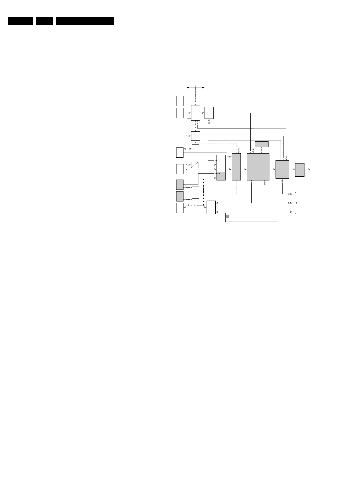
EN 70 FM242 AB9.
Circuit Descriptions and List of Abbreviations
The PSU consists of a pre-conditioner part and a DC/DC
converter part. This converter supplies power to the PDP high
voltages, the auxiliary voltages, and the audio amplifier. There
is a separate standby power supply, which supplies the Main
Processor, PDP microcontroller, interrupt generator and some
other circuits.
The mains inlet module will host the inlet and filtering.
There is a functional "Mains on/off" switch on the LED panel.
This switch is on the secondary side, controlling the relays on
the primary side.
9.2 Power Supply Unit (Diagrams P)
The Power Supply Unit (PSU) is designed to provide regulated
output voltages for the plasma display panel (PDP) and the
built-in electronic panels (such as e.g. the SCAVIO and Audio
Amplifier panels).
It will house the Pre-conditioner, DC/DC converters and the
Standby circuitry. In addition, this panel will house the
protection and the (optional) fan drive circuitry.
For Service this supply-panel is a black-box.
When defect (this can be traced via error-codes in the error
buffer, or by strange phenomena), a new panel must be
ordered, and after receipt, the defective panel must be send for
repair.
In that case before sending it, check if the supply-output lines
match with the values on the pdp-sticker.
9.3 VGA Connector Panel (Diagram VGA)
The Video Graphics Array (VGA) panel serves as an interface
between the peripheral VGA equipment (Receiver box, PC,
etc.) and the SCAVIO panel. Some specifications of this panel:
• Two NVMs are present, which hold identification data for
the DDC line.
• Further, there are buffers present for the incoming and
outgoing sync signals.
• RC_OUT cinch for linking with other equipment.
• Provision to terminate the incoming sync lines with 75 Ω via
the EBOX_PRESENT line.
For a description, see the next SCAVIO chapter.
9.4 SCAVIO Panel (Diagrams SC)
The Scaler Control Audio Video Input Output (SCAVIO) panel
contains:
• All the input connectors,
• Analogue and digital video processing,
• Scaler (co-processor)
• Interface to the PDP,
• Audio processing (excluding the audio amplifier),
• OTC (main processor), and
• RS232C in/out.
Note: There are two versions of this panel, a Basic and an
Enhanced version. Therefore, a lot of components are
therefore not mounted for the Basic version.
For the circuit description, we divide the board into the following
parts:
1. Supply
2. Video processing
3. Audio processing
4. Control
9.4.1 Supply
See figure "Power Supply Part" in paragraph 9.1.5. (even
opletten dat hij goed verwijst)
9.4.2 Video Processing (Diagrams SC3, 4, 5, 6, 10, 11 and 12)
Introduction
7225
SAA7118
Dig.
Video
dec.
7025
sync.
decoder
switch
NVM
DDC
7088, 7090
YPbPr
RGB
NVM
DDC
NVM
DDC
digital
processing
path
7280
De-int.
15,6 KHz = 1fH
31,2 KHz = 2fH
RGB
RGB
RGB
SWITCH
(SW-
download)
TMDS
H+V sync
7146, 7158
AD9887
2fH
Video+
sync.
switch
TXD/RXD-PW
TXD/RXD-OTC
RGB
ADC
RGB
dig.
+
TMDS
DECODER
! All Functional blocks shaded grey are required for
the"Basic Configuration".
The remainder is required for the "Enhanc ed Configuration".
YUV2fH progressive
dig.
I2C BUS 3
MEMORY
76057170
PW164
Pixelworks
7656
RGB
dig.
EPLD
I2C BUS 1
I2C BUS 2
7670
RGB
dig.
LVDS
to OTC (7383)
CL 26532038_011.eps
analogue
processing
path
AV1
CVBS
YC
AV2
0375
DVI-d
HD
AV3
Flex
VGA
2
VGA
1
RS
232
1fH
Figure 9-3 Video path
This mainly consists of a small analogue processing part and
a larger digital signal processing part.
The video inputs like CVBS, YC, High Definition RGB, or YUV
(1fH and 2fH), VGA, and DVI-D are received and processed.
The YPbPr (2fH) is discretely converted to RGB, whereas the
YCbCr (1fH) is processed in the SAA7118 Digital Video
decoder. The base-band video inputs (CVBS and YC) are
output from the digital video decoder as digital YUV, which are
then further processed by the PixelWorks Scaler.
The VGA signals are first AD converted and then processed by
the PW Scaler.
The digital input on the DVI is first decoded by the TMDS
decoder inside the AD9887 and then processed by the PW
Scaler.
The PW Scaler output is going through an EPLD and then via
the LVDS transmitter to the PDP (Plasma Display Panel) as
differential serial data.
Analogue Video
This part describes the analogue video and synchronisation
path of all inputs, until it reaches the "analogue digital
converters" of either the AD9887 (ADC+TMDS Decoder) or the
SAA7118E (Digital Video Decoder).
Also the switching part is described and the necessary control
signals.
In principle, all video control functions are done by the
PixelWorks processor.
Note: This part also includes the VGA connector panel that is
mounted on top of the SCAVIO panel.
Inputs
There are five video inputs, which are divided in three types:
• VGA (2fH): named VGA1 and VGA2. Both are 15-pole
SUB-D connectors for RGB and HV, and are situated on
the VGA connector panel. For automatic identification by a
PC, each VGA input is foreseen with a DDC NVM IC. VGA2
is set default as loop through of VGA1. In the Enhanced
to PDP
240402
Page 71

Circuit Descriptions and List of Abbreviations
EN 71FM242 AB 9.
version, VGA2 can be switched as output, via the control
signals VGA2_OUT and VGA2_EN.
• YPbPr/RGB (combined 2fH and 1fH): named AV3 and
suitable for YCbCr/HD-YPbPr/HD-RGB + HV. These are
cinch inputs. YPbPr and RGB are seen as separate inputs
by the HW and must be properly selected by SW.
• CVBS like (1fH): named AV1 for CVBS and AV2 for Y/C.
These are also cinch inputs.
Video Path
The 1fH signals (including YPbPr) are buffered (item 7113/21/
17) and go directly to a digital video processor, the SAA7118E
(item 7225 on diagram SC5), where they are converted into a
digital signal.
The 2fH signals are also buffered; both YPbPr (item 7074/84/
79) and RGB (item 7141/38/35) buffers get the same input
signals.
When YPbPr signals are connected, the correct input must be
selected, to get a picture with proper colours. Thus, the signals
must pass a video matrix (item 7088/90, see diagram SC3),
where they are converted into RGB. There are two matrices, an
NTSC and an ATSC. With the MATRIX_SEL signal, the correct
matrix is chosen (item 7089). The detection is done automatic,
by an algorithm in the EPLD.
After the matrix, the signals enter a clamp/blanking circuit
(7102/03/04 and 7100), for the removal of the residual sync
signals. The control is done via the lines HD_BLANKN and
HD_CLAMPN coming from the EPLD.
All RGB signals come together at 4-pole switches (item 7146/
58), one for each colour, where they are switched to the AD
converter item 7170 (R_ADC, G_ADC and B_ADC).
Sync Path
All incoming H and V sync signals go to a 4-pole switch (item
7009) where SYNC_SEL and VIDEO_SEL_2 determine, which
signal is available on the ADC.
Before this switch, the VGA sync path is rather straight, only 1
switch (item 7007) is added for the VGA2 sync signals, which
determines if VGA2 sync is input or output (VGA2_OUT).
In the Basic configuration, these switches are omitted, and
replaced by jumpers (4009/4010).
The external sync (AV1 - 3) signals are treated differently. Both
H_HD_EXT and V_HD_EXT go to three circuits:
• A comparator circuitry with an LM319 (item 7025), to
ensure both sync pulses are always positive going (H and
V_SYNC_CMP),
• A level detection circuitry (items 7000 to 7002), to detect if
the sync is of TTL level (H and V_SYNC_TTL),
• A positive/negative going detection circuitry (items 7006 to
7010), to indicate the polarity of the sync in case of TTL
level (H and V_SYNC_POL_N).
All above-mentioned signals go to the EPLD (see also diagram
SC11) for further processing.
Processed sync signals H_HD and V_HD coming from the
EPLD, are also switched to the ADC (H_ADC and V_ADC)
along with the proper RGB signals (R_ADC, G_ADC and
B_ADC).
Digital Video
This part describes the digital video path on the SCAVIO panel,
starting at the AD converters in either the AD9887 (item 7170)
or in the SAA7118E (item 7225) and ending at the output for the
PDP.
For both the Basic as the Enhanced version, everything "after"
the PixelWorks chip, is equal.
For the Basic version, the input for the PixelWorks only
consists of the "Graphics path".
For the Enhanced version, it is both the "Graphics path" as the
"Video path".
The SCAVIO panel contains the following functions in the video
path:
1. The "YPbPr to RGB matrix" and "2fH Video+Sync Switch"
are explained above in the "Analogue Video" part.
2. The "Digital Video" path containing the Digital Video
Decoder and the De-interlacer.
3. The "Digital Graphics" path containing the ADC+TMDS
decoder.
4. The "Scaler" which is the PixelWorks (PW164-10R) plus
Memory.
5. The "EPLD" for sync decoding and video manipulation.
6. The "LVDS" encoder.
The Digital "Graphics Path"
This is a straightforward application of the Analogue Devices
AD9887 (item 7170). Inputs for this device are:
• FTV Receiver box,
• VGA formats (up to SXGA@75 Hz),
• 2fH RGB+HV (only in Enhanced version),
• 2fH YPbPr, which is converted to RGB by the "YUV to
RGB" matrix (only in Enhanced version),
• DVI-d (only in Enhanced version).
Analogue input: The AD9887 is meant to sample "pixel
synchronous". To achieve this, a (software) driver is running on
the PixelWorks processor (PW). After hooking up a source to
the AD9887, the PW starts counting the number of lines per
field and calculates the H-period time. With these two values, it
determines the exact match or the closest match out of a lookup-table (LUT) with VGA standards. When the correct standard
is determined, the PW will set the AD9887 I
correct value. The AD9887 should now sample with exact the
same frequency as the incoming standard requires. This is
done to get an optimal picture performance.
It also is a "must" when a computer graphics card is connected,
because there is no, or very little, post anti-aliasing filtering
done on such cards. Therefore, the outputted RGB samples
need to be exactly aligned with the sampling of the AD
converter.
Analogue input signals can go up to SXGA@75 Hz, which
gives a pixel clock of 135 MHz. In fact, it can handle any
standard with a pixel rate up to 140 MHz.
Special modes are made for the F21R E-box, for both PAL and
NTSC. These are invoked when an E-box is connected to the
SCAVIO panel.
Digital input: Via the DVI connector (Enhanced version only)
it is possible to insert TMDS (Transition Minimised Differential
Signalling) data into the SCAVIO panel. DVI is a fairly new
computer graphics standard, which can be seen as the digital
follow-up of the analogue VGA interface. The TMDS signal is
directly fed into the AD9887, where any DVI standard up to
SXGA@60 Hz can be decoded to RGBHV.
The preferred VGA standard for the FM242 is programmed in
the DDC EEPROM (item 7215), which can be read by the PC.
Via an internal switch, it is possible to choose between the
analogue input and the digital input. The output format is for
both inputs the same (8 bit RGB plus HV). The driver
determines whether the AD9887 outputs single or dual pixels.
For lower standards like VGA@60Hz, the interface will be
single pixel, which means that every clock cycle one byte of R,
G, and B data is outputted. Dual pixel means that on every
clock cycle two bytes of R, G, and B data outputted. These two
bytes are de-multiplexed, which is done to make the interface
more robust for jitter, set-up, and hold times, and to reduce the
digital data rate over the PCB (reduced EMC).
Digital "Video Path"
This path is only available in the Enhanced version of the
SCAVIO panel and is used for the following input signals:
• CVBS input,
• Y/C input, and
• 1fH YPbPr.
2
C registers to the
Page 72
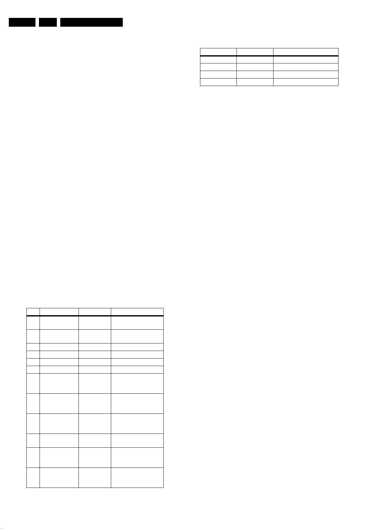
EN 72 FM242 AB9.
Circuit Descriptions and List of Abbreviations
It is a straightforward application of the Philips SAA7118 (item
7225) and the Micronas SDA9400 (item 7280).
The SAA7118 is a PAL/NTSC/SECAM Digital Video Decoder
with adaptive digital comb filter and component video input. It
decodes all input standards to 4:2:2 YCbCr, which then is
processed by the SDA9400.
The SDA9400 is a motion adaptive de-interlacer, which makes
a progressive video signal from the interlaced input.
Depending on the motion in the picture, it will just interleave the
odd and even field (no motion: ABAB) or repeats the same field
twice; this is also known as line doubling (motion: AABB). The
motion detection is pixel based, with a soft-switch between
"motion" and "no motion".
After the de-interlacer, the signal is fed as a 4:2:2 YCbCr
progressive scan signal to the video port of the PixelWorks
processor.
The PixelWorks PW164 Scaler
The PixelWorks PW164 Image Processor is a highly integrated
(Ball Grid Array, BGA) chip, which interfaces video inputs and
computer graphics in virtually any format to the PDP.
Computer images from VGA to UXGA resolution input to the
chip can be resized to fit on the PDP. Horizontal and vertical
image scalers, coupled with intelligent frame locking circuitry
create sharp images, centred on the screen and without user
intervention. An embedded DRAM frame buffer and memory
controller perform the frame rate conversion.
Video data from 4:3 aspect ratio NTSC or PAL and 16:9 aspect
ratio sources such as HDTV and DVD are supported. Nonlinear scaling (only with Receiver Box) and separate horizontal
and vertical scalers allow these inputs to be resized optimally
for the native resolution of the PDP.
For more information, see http://www.pixelworksinc.com/
index.phtml
Table 9-1 PixelWorks Scaler: Ports
Pin Name I/O Remark
C2 PW_SCL +3V3 output to I2C devices, Video
related
B1 PW_SDA +3V3 output to I2C devices, Video
related
A1 PW_SDA_NVM +3V3 output to I2C device NVM
C4 PW_SCL_NVM +3V3 output to I2C device NVM
B3 SCL_2 +3V3 output to I2C device OTC
A2 SDA_2 +3V3 output to I2C device OTC
A3 VIDEO_SEL_1 +3V3 output to video selection
switches (see truth
table)
C5 VIDEO_SEL_2 +3V3 output to video selection
switches (see truth
table)
B4 VGA2_OUTN +3V3 output Selects VGA 2 as
output. (Low =>
Output)
A4 VGA2_EN +3V3 output Enables VGA 2 (High
= Enable)
C6 SYNC Input Is "high" if EPLD
detects separate sync
signals on YPbPr
B5 1_2FH Input Is "high" if sync on
YPbPr is 1fH (from
EPLD)
Table 9-2 PixelWorks Scaler: Video Select
VIDEO_SEL_1 VIDEO_SEL_2 Selected input for AD9887
00RGB 2fh
0 1 YPbPr 2fh
1 0 VGA 1
1 1 VGA 2
Service remark: Desoldering/soldering of this BGA-ICs
requires very specialised (BGA) equipment. This can only be
done by the full-equipped service repair workshops. (See also
chapter “Safety Instructions, warning and notes”).
The EPLD
The main reason to add the EPLD, is the contrast reserve
function. Other reasons:
• Black and white ADC adjustment. The EPLD provides a
high-resolution measurement of the black and white level,
to adjust the gain and offset of the ADC (AD9887). It is read
2
via I
C.
• LVDS reset. This function resets the LVDS transmitter on
the SCAVIO board, in case the LVDS transmitter starts up
without a clock. This could cause an abnormal picture.
Therefore, as soon as the clock is not fast enough (as
during start-up) the EPLD will keep the LVDS transmitter in
reset.
• Receiver-box mode detection. For loop through mode (a
second FTV monitor connected to the output of the first
monitor), a secondary detection is needed to check the
presence of an Receiver or E-box.
• ATSC sync detection/ decoding. Core for proper sync
decoding for ATSC sources.
• Contrast reserve. This function can increase the gain of
the video signal to a factor of two. It will reduce the gain
again if it sees too many overflows (code 255) in any of the
R, G, or B channels. Adjustable via two parameters: user
contrast and overflow limit. Parameters are I
2
C controlled.
The LVDS transmitter
This DS90C385MTD56 IC from National Semiconductors
converts 28 bits of CMOS/TTL data into four LVDS (Low
Voltage Differential Signalling) data streams. A PLL transmit
clock is transmitted in parallel with the data streams over a fifth
LVDS link. Every cycle of the clock, 28 bits of input data are
sampled and transmitted. At a transmit clock frequency of 36
MHz, 24 bits of RGB data and 3 bits of display control data are
transmitted per LVDS data channel. This IC operates at 3.3 V
For more information, see http://www.national.com/
Picture Mute
In some cases, it is necessary to mute the video output:
• In Monitor mode:
– During switch "on/off" of the monitor,
– During source change,
– During video or sync loss, or
– By a user action (A/V-mute or mute)
– In audio only mode (when the ICONN-box is
connected).
• In TV mode:
– During switch "on/off" of the Monitor/Receiver box,
– During source change in the Receiver box,
– During video or sync loss, or
– In audio only mode (Receiver box mutes the picture).
Most of the picture mute controls are done via the PixelWorks
co-processor.
Anti Ageing
In order to prevent visible luminance differences, due to ageing
of the monitor, a special algorithm is implemented. This
algorithm is based on horizontal shifting of the picture in the
Page 73

Circuit Descriptions and List of Abbreviations
EN 73FM242 AB 9.
monitor. For good understanding some terms will now first be
explained:
• Ageing: The effect that the efficiency of a plasma cell
(pixel) decreases as a function of the total time that it is
illuminated. This effect occurs mostly because of phosphor
ageing. As a result, the cell brightness decreases over
time. An alternative name for ageing is "burn-in".
• Picture shifting: Fixed structures, like logo"s, OSDs, and
subtitles, will cause burn-in effects. The only way to mask
this to a certain extends, is picture shifting so that the
"burn-in" effect is smeared out over a larger area, and
makes it less visible.
Most of the anti-ageing controls are implemented in the
PixelWorks co-processor.
Horizontal
Horizontal anti-ageing steps:
• Step width/height, the step width/height shall be 1
horizontal pixel width (approx. 1 mm).
• Number of steps, the maximum number of steps in
horizontal direction shall be 9.
• Time between steps, the time between the steps shall be
5 minutes.
The effect of H anti-ageing is a horizontal movement (start at
0):
0 → 1 → 2 → 3 → 4
12 ← 11← 10 ← 9 ← 8 ← 7 ← 6 ← 5 ←
→ 13→ 14 → 15
With the following sequence:
0 → 1 → 2 → ...... → 14 → 15 → 0 → 1 → etc.
After every step, the updated value is stored in NVM and gives
an indication about the direction (0...4 and 13...15 to the right
and 5...12 to the left).
The horizontal anti-ageing is a process, which is basically
independent of any other processes that are running in SW.
This means that this process should never be reset in order to
get the best anti-ageing effect. Therefore, the horizontal shift
positions and directions need to be stored in NVM, so that he
anti-ageing process returns to its latest position after the set
has been switched off or to standby. There is only one H and
one V shift value for the anti-ageing process that is applicable
for the AV1, AV2, and AV3 inputs.
Note: Horizontal shift cannot be done for sources that are
screen filling and do not have sufficient overscan.
↓
9 15
↓ ↑
10 14
↓ ↑
11 13
↓ ↑
12
With the following sequence:
0 → 1 → 2 → ...... → 14 → 15 → 0 → 1 → etc.
After every step, the vertical shift position and its direction are
stored in NVM. So the anti-ageing process returns to its last
position after the set has been switched off (or to standby).
Also, if by any cause (i.e. VGA-source selection or when
service/factory mode is active), the anti-ageing process is
stopped; the vertical shift position should be restored after
resuming the anti-ageing process.
9.4.3 Audio processing (Diagrams SC13, 14 and 15)
This chapter describes the audio processing on the SCAVIO
board. The circuit enables to connect several audio sources,
selects the source on the desired input, and performs audio
processing and audio delay. It also matches the output signals
for the Audio Amplifier panel.
The sound-related electronics for FM242 are very straight
forward, and consists of a Micronas MSP3415G sound
processor, an active high pass and low pass filter, and
separate Class-D amplifiers for woofers and tweeters.
Vertical
V-shift is done in the F21R Receiver box when the TV mode is
active, or in the enhanced configuration when the monitor
mode is active.
Vertical anti-ageing steps:
• Height/height, the height/height shall be 1 display line
(approximately 1 mm).
• Number of steps, the maximum number of steps in
vertical direction shall be 9.
• Time between steps, the time between the steps shall be
80 minutes, which equals one complete horizontal ageing
shift (16 steps x 5 minutes).
The effect of V anti-ageing is a vertical movement (start at 0):
4
↑ ↓
3 5
↑ ↓
2 6
↑ ↓
1 7
↑ ↓
0 8
Page 74
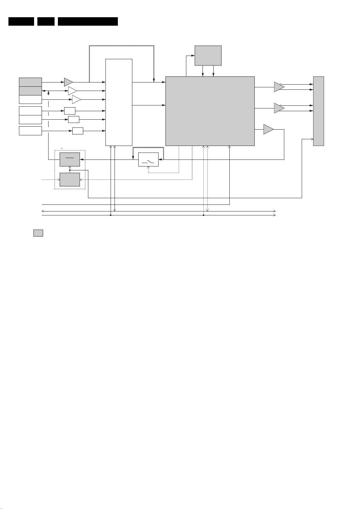
EN 74 FM242 AB9.
Circuit Descriptions and List of Abbreviations
Audio
inputs
VGA1
Audio-VGA-in
VGA2
Audio-Flex-VGA
DVI-D
Audio-DVI
AV1
Audio-CVBS
AV2
Audio-YC
AV3
Audio-YPbPr
Power-ok
MSP-Reset
I2C-SDA
I2C-SCL
(Enhanced only)
(Enhanced only)
(Enhanced only)
7801 : 7808
-4dB
-4dB
Mute
Logic
&
-4dB
-4dB
(Basic only) 7880
7798
(Enhanced only)
Matrix
Switch
TEA6422
Out 1
Out 2
Out 3
PRE-out1 (L)
PRE-out2 (R)
(Basic only)
(Enhanced only)
Switch
7800
-4dB
-4dB
(Enhanced only)
(Enhanced only)(Enhanced only)
(Enhanced only)
(Enhanced only)
(Enhanced only)
In 4
In 5
In 6
In 2
In 3
In 1
I2C-SDA
I2C-SCL
SCART1-in
SCART2-in
I2C
I2S-DA-Out
D-CTRL-0
Digital Audio
Delay Line
T1 T2
I2S
AUDIO DSP
D-CTRL-1
II2S-DA-In1
MSP3415
I2C-SCL
I2C-SDA
I2S7812
I2S-DA-In2
MSP-Reset
DACM-L
DACM-R
SC1-OUT
+3.0dB
2* Differential
Amplifier
7841
+4.9dB
7851
+4.9dB
0388
L-NEG
L-POS
R-NEG
L-NEG
Audio out (to Audio Amplifier)
Audio Enable
= Only for Basic configuration.
Figure 9-4 Audio Path
The processing part consists mainly of the following
components:
• MSP3415G: a DSP sound processor from Micronas. This
component is able to do all kinds of digital signal
processing like volume, bass/treble, UltraBass and
balance. It has analogue inputs and outputs, as well as an
2
I
S in/output used for digital audio delay.
• RAM with its logic to be able to store the I
2
S information for
audio delay.
• Anti-plop/ mute circuit: which is necessary to prevent
disturbances on the audio lines during start-up or
switching.
• TEA6422: a matrix switch of ST. This component is able to
switch six inputs to three different outputs (only used in the
Enhanced version).
MSP3415G
Ultra Bass
Because of the closed box implementation in FM242, a
common DBE solution will not give an optimal bass
performance. A closed box needs a substantial boost over a
wide frequency range, while DBE operates in a limited
frequency region.
Adaptive Ultra Bass 2 (UB2) is a suitable alternative. This
feature is based on the psycho-acoustic effect of the missing
fundamental, and gives the impression of a deep bass while
the loudspeakers do not reproduce these low frequencies. This
feature is implemented in the MSP3415G.
Audio delay
To compensate for "lip sync error" (the difference in time
between the aural and visual perceptions), two different audio
delays are selectable via the customer"s menu (one for the
Receiver box and one for the Monitor).
This is done at the audio processor IC7812 via an I
an additional delay circuit (IC7880 - 7882).
One can select delays of 24 ms (I2S_DATA_IN1) and 40 ms
(I2S_DATA_IN2), or no delay.
In case of a delay, the AUDIO_L/R_IN is re-routed as
I2S_DATA_OUT to the audio delay circuit and, depending on
the selected delay, returned as I2S_DATA_IN1 or
I2S_DATA_IN2, resulting in AUDIO_L/R_OUT.
Anti-plop/Mute
In several cases, it is necessary to mute the sound output. This
muting is handled by the MSP sound processor, or by the
Receiver box in case of TV-mode.
• In Monitor mode:
– During switch "on/off" of the monitor.
– During source change.
– During video or sync loss, or
– By a user action (A/V-mute or mute).
• In TV mode:
– During switch "on/off" of the Monitor/Receiver box.
– During source change in the Receiver box.
– During video or sync loss, or
– By a user action (mute).
9.4.4 Control (Diagrams SC7, 8 and 9)
Introduction
As a main controller, better known as OTC (On screen display,
Teletext and Control). It is a 8051 (XA) based controller from
Philips Semiconductors, the SAA5801H.
Although the OTC is the main controller, it acts as a "slave"
when communicating with the PixelWorks IC via the I
When the monitor is connected to an F21R Receiver box, the
UART commands from the Receiver box will control the
monitor.
CL 26532038_012.eps
280302
2
S bus and
2
C-bus 2.
Page 75
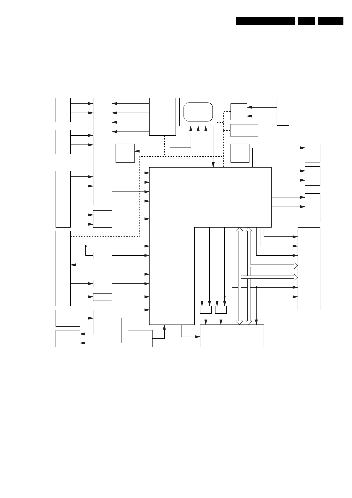
Circuit Descriptions and List of Abbreviations
EN 75FM242 AB 9.
In stand-alone mode, the monitor can be controlled via the
Remote Control or via the RS232C port.
DDC1/2B (Display Data Channel, an I
2
C based protocol) is
implemented with separate NVMs for the two VGA inputs and
the DVI-D input as well.
OTC Processor
7340 7540
UART
RS232
SWITCH
SYNC
DETECT
RESET
5V TEST
8V TEST
SELECT-1
SELECT-2
SELECT-3
SELECT-4
7812
AUDIO
(MSP)
RS-232-ACT
UART-ACT
TXD-OTC
RXD-OTC
SYNC-ACT
I2C-1
3V3-STBY
RESET
STANDBY
POWER-OK
5V-TEST
8V-TEST
MSPRESET
7383
EXPANDER
SAA5801
IO
PCF8574
I2C-1
POWER
DOWN
RS232
VGA2
(FLEX)
VGA1
PSU
TXD
RXD
VGA2-TXD
VGA2-RXD
VGA1-TXD
VGA1-RXD
VGA1-H
VGA1-V
5V
8V
PDP
PDP-GO
OTC
ROM-CS
It is also possible to use the RS232C port for software upload
to the PW Scaler and the OTC. The target for downloading is
controlled via a switch in the RS232C path; the switch itself is
controlled by the OTC.
CPU-GO
IRQ-PDP
RAM-CS
ROM-OE
RAM-OE
7530
ADC
GENERATOR
7656
EPLD
CLOCK
TEMP-1
TEMP-2
CLOCK
GENERATOR
NVM-WE
I2C-NVM
RED-LED
GREEN-LED
PW-RESET
PW-START
I2C-2
RAS
CASL
CASH
AC(0:9)
DC(0:15)
7500
7430
NVM
OTC
LEDS
7605
PW
DRAM
RC
RECEIVER
RC-OUT
RC5-IN
RC-CNTL
SERVICE
INPUT
SERVICE_IN
Figure 9-5 Control Part
This part describes the Main Control part of the SCAVIO panel
and the interfaces with the software. The control function
consists of the following tasks:
• Control of external IOs, like fan speed, temperature,
service and RC5,
• UART communication with Receiver box,
• RS232 control / communication,
• Supports the uploading of new SW into the Flash-ROMs,
• Start-up of monitor and initialisation via I
2
C,
• Error detection and storing.
Start-up and Shut-down
The POR signal is not generated on the PSU, but on the
SCAVIO board. This is done with a fully integrated ADM810T
POR chip (item 7517), which senses the 3.3 V coming from the
PSU. The sense level is 3.08 V. During power-up as well as
power-down, this chip will make the RESET signal high. During
WP
7506
&
&
WE
AC(0:20)
7510
DC(0:15)
FLASH ROM
CL16532099_004.eps
170801
power-up, this signal will be held "high" until 240 ms after V
has become stable.
During power-down, the system will be reset as soon as the
V
drops below 3.08 V.
CC
Start-up from Standby
When the monitor is in standby mode, it can wake-up in several
ways:
• When an RC command is received (RC_IN).
• Detection of H- and/or V-sync on VGA1.
• Detection of UART communication on VGA1.
• Detection of RS232 communication.
• Detection of Service modes.
RC Command Reception
When a RC command is received at the RC receiver on the
LED panel, it will go directly to the RC input of the OTC (RC_IN
CC
Page 76
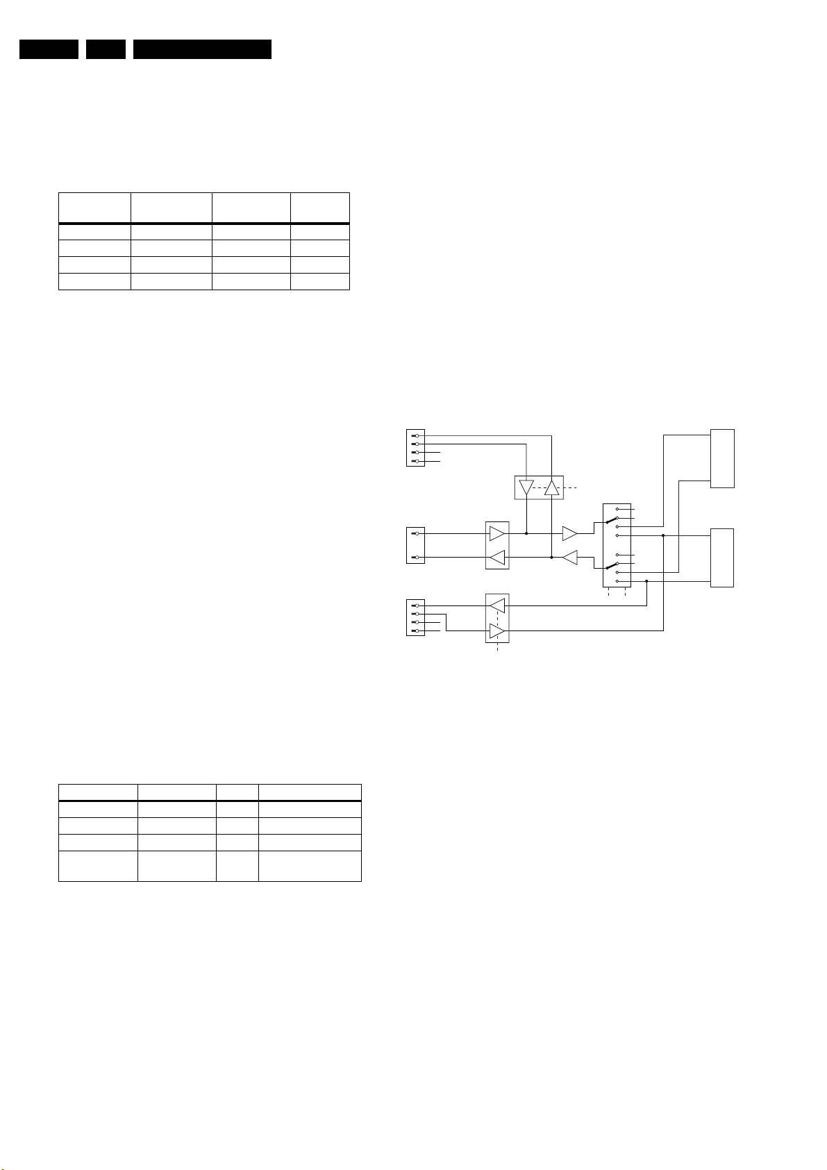
EN 76 FM242 AB9.
Circuit Descriptions and List of Abbreviations
on pin 100). If the monitor is in standby, and a proper RC
command is send, it will wake up.
The RC commands are routed to the Receiver box via the
VGA1 connector pin 9 (RC_VGA1), but this loop through
connection is controlled by RC_CNTL. Below is the truth table.
Table 9-3 RC Commands overview
RC
F21REE-box FM242Monitor
commands RC_CNTL
In Standby In Standby Send to E-box Low
In Standby On Blocked High
On In Standby Send to E-box Low
On On Send to E-box Low
Note: All RC commands are direct available on a separate RCout cinch connector (RC_OUT) on the VGA connector panel.
H- and/or V-sync Detection
When both H and or V sync are present on VGA1, there is a
pulse (low) on SYNC_ACT. When only H is present,
SYNC_ACT is continuously low. The SW disables the
interrupt, once an interrupt is received.
UART Communication Detection
When there is UART communication on VGA1, the UART
detection circuitry generates on every falling edge a pulse on
UART_ACT. This is a negative going pulse with a width of ±
470 s. The first pulse will trigger the main software to check for
the FTV System Protocol (FSP). The SW disables the interrupt,
once an interrupt is received.
RS232 Communication Detection
When an RS232 connection is made, and communication is
started (pulses on RS232_RXD), RS232_ACT becomes
"high". Via a transistor, RS232_ACT will make SERVICE_IN
low. When the Monitor is operating (+5 V available), this signal
is made low (in fact it is disabled).
Service Mode Detection
It is possible to enter four different Service Modes (provided the
OTC is still supplied by the +3V3_STBY).
Via the SERVICE_IN signal, which is an ADC input of the OTC,
a voltage drop is detected from +3.3 V to V
V
is a DC voltage, which represents the mode to be entered:
X
.
X
Table 9-4 Service Mode levels
Service mode Limits Vx [V] Vx [V] Remarks
SDM 3.0 > Vx > 2.4 2.6 0382-2 to GND
SAM 2.4 > Vx > 1.8 2.0 0382-4 to GND
COMPAIR 1.8 > Vx > 1.2 1.4 0382-6 to GND
RS232 active Vx < 0.8 >0.8 Plug in RS232, start
program
2
I
C
There are four I
overview in chapter 6):
2
• I
C bus 1 is a (5 V) device bus, controlled by the OTC, and
2
C busses used in the monitor (see also I2C
connected to the following devices:
– PDP.
– EPLD.
– IO expander SCAVIO - PCF8574A.
– IO expander PSU - PCF8574A.
– ADC - PCF8591.
– Clock generator for PW - FS6377.
– Sound processor MSP3415G.
– Audio switch TEA6422 (Enhanced version only).
2
• I
C bus 2 is used for communication with the PixelWorks
co-processor (PW). Although the OTC is the main
controller, it will act in this case as a "slave", since the PW
can only act as a "master". Before any I
2
C commands are
exchanged, the PW gets an interrupt (PW_START) to
indicate that the OTC wants to talk to the PW.
2
C bus 3 is a (5 V) device bus, controlled by the PW, and
• I
connected to the following devices:
– Video Decoder SAA7118 (Enhanced version only).
– De-interlacer SDA9400 (Enhanced version only).
– ADC/TMDS receiver AD9887.
– 3D Comb filter MN8783LSI (optional).
2
C bus 4 is a (5 V) device bus, only connected to the NVM
• I
(to avoid data corruption).
Notes:
• The PDP and EPLD are in fact 3.3 V bus devices, but they
need to be connected to bus 1, since the OTC is the first
controller to be fully operating at start-up. For this reason,
2
an I
C level shifter (items 7675/76 on diagram SC12) is
included, which converts the 5 V signals into 3V3 and visa
versa.
• One of the first commands is to set the clock generator
(item7570), else the PW can not start-up.
RS232/UART
(FLEX VGA)
VGA2
15 pin Sub-D
RS232
9 pin Sub-D
VGA1
15 pin Sub-D
VGA2_TXD
4
VGA2_RXD
11
12
15
3
2
4
VGA1_TXD
11
12
VGA1_RXD
15
ST232
74HCT
125-A/B
S1
74HCT
125-C/D
RXD
TXD
S4
74HC4052
n.c.
n.c.
n.c.
n.c.
S3 S2
Figure 9-6 RS232/UART
Introduction
The FM242 monitor is equipped with an RS232 interface. Via a
9 pin Sub-D connector, it is possible to connect a PC for special
modes like:
• SW download.
• Factory purposes.
• Service.
• Professional use.
A second option is the connection of a so-called ICONN-box for
Institutional TV (Hotel TV).
For communication with the Receiver Box, UART is used,
because this protocol can handle longer cable distances than
2
I
C. The (Receiver box) UART is interfaced via a 15 pin Sub-D
connector (VGA connector). Via this UART connection, the
F21R Receiver box and the FM242 Monitor can communicate
(via FSP). By doing so, the monitor will know that there is an
Receiver box connected and thus it is operating as a TV
configuration.
RS232/UART Control
The OTC (SELECT_1 to 4) controls the RS232/UART
switches. When the monitor is in Receiver box mode, there is
no RS232 communication possible. The monitor is default set
in Receiver box mode (switch to n.c. position) and the UART
from/to VGA1 is enabled, to allow communication with
Receiver box.
If no Receiver box is detected, the UART is disabled to ensure
that there will be no communication towards the OTC, and the
RXD-PW
PW
TXD-PW
RXD-OTC
OTC
TXD-OTC
S1..S4 = control signals
S1 = SELECT_1
S2 = SELECT_2
S3 = SELECT_3
S4 = SELECT_4
CL 26532038_013.eps
280302
Page 77
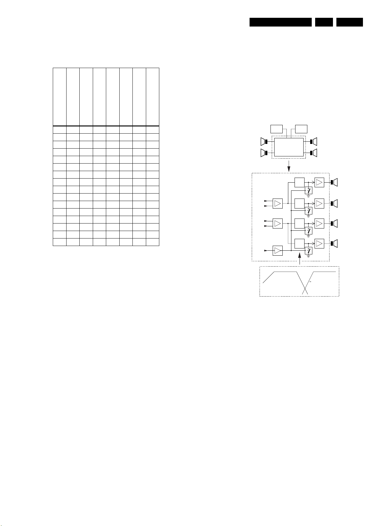
Circuit Descriptions and List of Abbreviations
EN 77FM242 AB 9.
switch is set to OTC. Below the truth table of the switches is
shown, which determine the TXD/RXD path.
Table 9-5 RS232/UART Control
S1= SELECT_1 (P0)
S2 = SELECT_1 (P1)
S3 = SELECT_1 (P3) (3)
S4 = SELECT_4 (P4) (4)
UART VGA1 (E-box)
UART VGA2 (flex)
RS232 set to OTC (1)
RS232 set to PW (2)
00000000
00010000
00100000
00111000
01000000
01010000
01100000
01111000
10000000
10010010
10100100
10110000
11000000
11010001
11100100
11110000
(1) Software download or ComPair mode.
(2) Software download or Debug mode.
(3) When S3 = 1 the 74HCT4052 is in a tri-state ("off" state).
(4) When S4 = 0 the TXD out of RS232 is disabled (S4 may not
become low in any other case).
UART Detection
When the VGA1_RXD line is continuously "low", the OTC
might run slow due the fact that so-called "break" signals are
generated. To prevent this, a small circuitry is added to detect
whether VGA1_RXD is continuously "low" (item 7310).
When the VGA1_RXD line is "low" for about 20 ms, the bufferswitch (item 7303-A) is opened. After this buffer, a second
discrete buffer is placed (items 7315/16), which keeps the
RXD_OTC line "high" and changes the 5 V into a 3.3 V level.
ICONN-box
For application of a Flat TV in a hotel environment, the monitor
is designed to operate with a so-called ICONN-Box. The
ICONN-box will take over the user control of the monitor, by
intercepting the RC5-commands coming from a dedicated RCtransmitter, which sends specific hotel-mode commands and
sending its own RC-commands to the microprocessor in the
monitor.
So in the ICONN-Box, the hotel-mode commands will be
converted to RC5-commands, which than can be interpreted by
the monitor.
When connected to the RS232 input, this box takes over the
control of the IR-receiver in the monitor. It is also able to control
the front LED. The switches (7550 for the IR and 7555 for the
LED signals) are controlled by the ICONN_NOT signal.
The ICONN-Box shall interface the Monitor with the following
signals:
• IR-RX. These are the RC5-commands coming from the
specific hotel RC5 - transmitter, which are received via the
RC5-receiver of the monitor.
• IR_TX. These are the RC5-commands generated by the
ICONN-Box and send to the monitor.
• RL_ICN. Control signal from the microprocessor (of the
monitor), indicating the power state of the monitor. The
ICONN-Box and monitor LED are driven in parallel.
• GL_ICN. Control signal from the microprocessor (of the
monitor), indicating the functionality of the monitor, to drive
the LED on the ICONN-Box.
• LD_ICN. Control signal from the ICONN-Box to drive the
green LED on the monitor.
9.5 Audio Amplifier Panel (Diagram A)
9.5.1 Introduction
AUDIO
AMPLIFIER
MUTE
PSU
7260-A
L-HIGH
HPF
7238-A
L-LOW
LPF
7260-B
R-HIGH
HPF
7238-B
R-LOW
LPF
1kHz 3kHz
LOW
HIGH
(LPF)
(HPF)
TWEETER RIGHT
TWIN-CONE SPEAKER RIGHT
MUTE
MUTE
MUTE
MUTE
6dB/OCT
SCAVIO
TWEETER LEFT
TWIN-CONE SPEAKER LEFT
AUDIO AMPLIFIER
7225-A
L-POS
L-NEG
7225-B
R-POS
R-NEG
AUDIO
ENABLE
63Hz
Figure 9-7 Block diagram Audio Amplifier
This panel houses the audio filters and amplifiers necessary for
driving the speakers. The differential audio inputs (for common
mode immunity) come from the SCAVIO panel (via connector
0388).
The PSU delivers the positive and negative supply voltage of
14.5 V
, as well as the +9V_STBY voltage.
DC
After being filtered and amplified, the signals go to the speaker
section, where the (twin cone) low/mid range speakers and the
tweeters are driven (load impedance is 8 Ω).
9.5.2 Supply (Diagram A7)
The supply voltage is a symmetrical voltage of +/- 14.5 V
generated by the main supply via L5002.
• V
• V
(+14.5 VDC) on connector 0302 pin 5/6, and
SND_POS
(-14.5 VDC) on connector 0302 pin 1/2.
SND_NEG
9.5.3 Filter (Diagram A2)
Electrical filtering is needed for following reasons:
• Limiting the cone excursion, thereby reducing the
distortion.
• Increasing the power handling capacity (PHC).
In the FM242, active second order Sallen-Key filters are used,
with crossover frequencies of 1 kHz for the lowpass filter, and
3 kHz for the highpass filter.
L
R
CL16532099_003.eps
HIGH LEFT
MID/LOW LEFT
HIGH RIGHT
MID/LOW RIGHT
040402
DC
,
Page 78
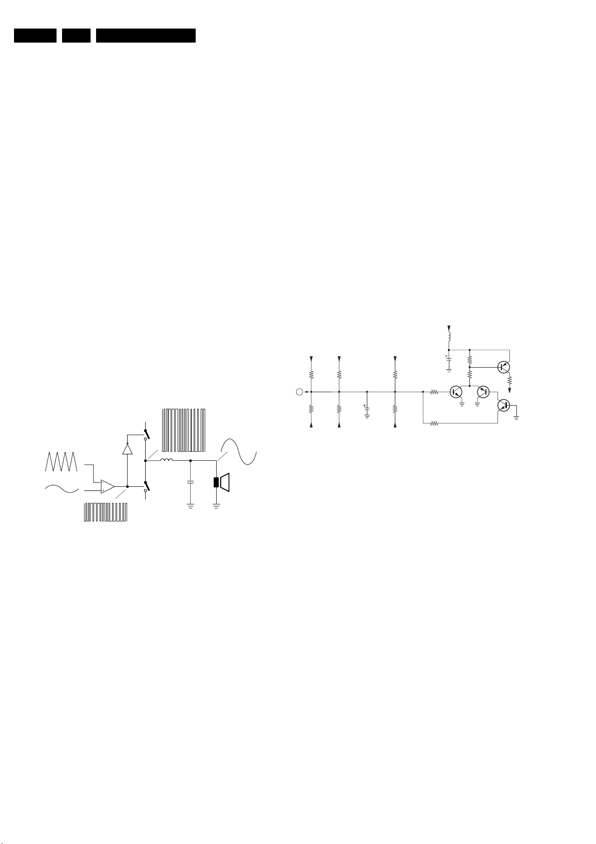
EN 78 FM242 AB9.
Circuit Descriptions and List of Abbreviations
The audio signals are filtered before the amplifier. There are
some reasons for doing this:
• It is now easy to do active filtering, and
• At less costs (no expensive coils and capacitors).
Low Pass Filter (LPF)
For L and R separately, a Low Pass Filter (IC7238A and B) is
processing L_LOW and R_LOW.
The output signal of this filter is then fed to the audio amplifier
(identical for right channel).
High Pass Filter (HPF)
For L and R separately, a High Pass Filter (IC7260A and B) is
processing L_HIGH and R_HIGH.
The output signal of this filter is then fed to the audio amplifier
(identical for right channel).
9.5.4 Amplifier (Diagrams A3 to A6)
Each speaker has its" own 15 W class-D amplifier. These
amplifiers combine a good performance with a high efficiency,
resulting in a big reduction in heat generation.
Principle
Audio-power-amplifier systems have traditionally used linear
amplifiers, which are well known for being inefficient. In fact, a
linear Class AB amplifier is designed to act as a variable
resistor network between the power supply and the load. The
transistors operate in their linear region, and the voltage that is
dropped across the transistors (in their role as variable
resistors) is lost as heat, particularly in the output transistors.
Class D amplifiers were developed as a way to increase the
efficiency of audio-power-amplifier systems.
+V
loss in the load, which causes lower efficiency. An LC filter with
a cut-off frequency less than the Class D switching frequency
(350 kHz), allows the switching current to flow through the filter
instead of the load. The filter is less lossy than the speaker,
which causes less power dissipated at high output power and
increases efficiency in most cases.
9.5.5 Mute (Diagram A2 to A6)
A mute switch (item 7302) is provided at the PWM inputs (item
7315, LM311). This switch is controlled by the
AUDIO_ENABLE line, which checks the availability of the
+9V_STBY voltage.
9.5.6 Protections
Short-circuit Protection (Diagram A3)
A protection is made against a too high temperature of
transistor 7355 in case of a short-circuit of output FET 7365-1.
Transistor 7340 is sensing the current through transistor 7355
via R3355, and activates the DC-protection line (see below) in
case the current becomes too high. This is the same for all four
amplifier parts.
DC-protection (Diagram A7)
+9V_STBY
5753
OUT_LH
A
OUT_RH
3770
3780
OUT_LL
3771
3781
OUT_RL
2760
VCC_10_POS
VCC_10_NEG
3775
3765
3750
3760
3752
2753
3751
7751 7761
7735
3754
DC_PROT
7755
CL16532099_001.eps
200801
-V
CL16532099_002.eps
200801
Figure 9-8 Principle Class-D Amplifier
The Class D amplifier works by varying the duty cycle of a
Pulse Width Modulated (PWM) signal.
By comparing the input voltage to a triangle wave, the amplifier
increases duty cycle to increase output voltage, and decreases
duty cycle to decrease output voltage.
The output transistors (item 7365 on diagram A3) of a Class D
amplifier switch from "full off" to "full on" (saturated) and then
back again, spending very little time in the linear region in
between. Therefore, very little power is lost to heat. If the
transistors have a low "on" resistance (R
), little voltage is
DS(ON)
dropped across them, further reducing losses.
A Low Pass Filter at the output passes only the average of the
output wave, which is an amplified version of the input signal.
In order to keep the distortion low, negative feedback is applied
(via R3308). A second feedback loop (via R3310) is tapped
after the output filter, in order to decrease the distortion at high
frequencies.
The advantage of Class D is increased efficiency (= less heat
dissipation). Class D amplifiers can drive the same output
power as a Class AB amplifier using less supply current.
The disadvantage is the large output filter that drives up cost
and size. The main reason for this filter is that the switching
waveform results in maximum current flow. This causes more
Figure 9-9 DC Protection
Because of the symmetrical supply, a DC-blocking capacitor,
between the amplifier and the speaker, is not necessary.
However, it is still necessary to protect the speaker for DC
voltages.
The following protections are therefore implemented:
• Via R3765 and R3775, each stabilised supply voltage line
(via items 7735 and 7745) is checked on deviations.
• Via R3770/3771/3780/3781, each amplifier output is
checked for DC-voltage.
Via R3765/3775, a virtual earth is imposed on point A. When
one of the supply voltages deviates, a DC voltage will occur on
this point. If point A is positive, T7751 will conduct. If it is
negative, T7761 will conduct.
Both cases will make T7735 conduct, so that the DC-PROT
signal will be made high. This ensures that the power supply is
rapidly trimmed back.
Capacitor C2760 will ensure that only DC-signals at point A will
activate the protection.
9.6 LED/Switch Panel (Diagram LD)
This panel contains:
• The red and green status LEDs,
• The RC input receiver,
• The light sensor, and
• The "on/off" switch.
All signals on this panel come directly from the SCAVIO panel:
• The LED and sensor signals (RED_LED, GREEN_LED
and LIGHT_SEN_IN) are routed to the OTC. When a F21R
Receiver box is connected, the sensor signal is routed to
Page 79

Circuit Descriptions and List of Abbreviations
EN 79FM242 AB 9.
the OTC of this box (via UART), where it will control the
HOP via I
• The RC signal (RC_IN) is routed to the OTC, the VGA1
connector, and the RC-out cinch connector.
• The signals to (+9V_STBY) and from (+9V_STBY_SW) the
"on"/"off" switch are routed to the PSU board.
2
C.
9.7 Plasma Display Panel (PDP)
9.7.1 General
The PDP, which is used in the FM242, is a product of SDI
(Samsung Display Industry) . When defect, a new panel must
be ordered, and after receipt, the defective panel must be send
for repair in the packing (flight case) of the new ordered panel.
9.7.2 Operation
Principle
Plasma displays work by applying a voltage between two
transparent display electrodes on the front glass plate of the
display. The electrodes are separated by an MgO dielectric
layer and surrounded by a mixture of neon and xenon gases.
When the voltage reaches the "firing level", a plasma discharge
occurs on the surface of the dielectric, resulting in the emission
of ultra violet light.
This UV light then excites the phosphor material at the back of
the cell and emits visible light. Each cell or sub-pixel has red,
blue or green phosphor material and three sub-pixels combine
to make up a pixel. The intensity of each colour is controlled by
varying the number and width of voltage pulses applied to the
sub-pixel during a picture frame. This is implemented by
dividing each picture frame into sub-frames.(for 50 Hz-mode
there are 12 sub frames, for the 60 Hz-mode there are 10 sub
frames). During a sub-frame, all cells are first addressed those to be lit are pre-charged to a specific address voltage then during the display time the display voltage is applied to the
entire screen lighting those that were addressed.
Each sub-frame has a weighting-factor. (Time-entity depends
on size and number of pixels on the screen). This is a purely
digital PWM control mechanism, which is a key advantage as it
eliminates any unnecessary digital to analogue conversions.
9.8 Abbreviation list
ADC Analogue to Digital Converter
AM Amplitude Modulation
AP Asia Pacific
AV External Audio Video
B/G Monochrome TV system. Sound
carrier distance is 5.5 MHz
BGA Ball Grid Array
BTSC Broadcast Television Standard
Committee. Multiplex FM stereo sound
system, originating from the USA and
used e.g. in LATAM and AP-NTSC
countries
ComPair Computer aided rePair
CVBS Composite Video Blanking and
Synchronisation
DAC Digital to Analogue Converter
DDC Display Data Channel (a protocol
based on I2C)
D/K Monochrome TV system. Sound
carrier distance is 6.5 MHz
DFU Direction For Use: description for the
end user
DNR Dynamic Noise Reduction
DRAM Dynamic RAM
DSP Digital Signal Processing
DTS Digital Theatre Sound
DVD Digital Versatile Disc
DVI-d Digital Visual Interface, d = digital only
EEPROM Electrically Erasable and
Programmable Read Only Memory
EMI Electro Magnetic Interference
EPLD Erasable Programmable Logic Device
EU Europe
EXT External (source), entering the set via
SCART or Cinch
FLASH Flash memory
FM Frequency Modulation
FSP FTV System Protocol
FTV Flat TeleVision
HP Headphone
I Monochrome TV system. Sound
carrier distance is 6.0 MHz
I2C Integrated IC bus
I2S Integrated IC Sound bus
ICONN Institutional CONNector
IF Intermediate Frequency
Interlaced Scan mode where two fields are used
to form one frame. Each field contains
half the number of the total amount of
lines. The fields are written in "pairs",
causing line flicker.
IR Infra Red
IRQ Interrupt Request
LATAM Latin America
LED Light Emitting Diode
L/L" Monochrome TV system. Sound
carrier distance is 6.5 MHz. L" is Band
I, L is all bands except for Band I
LS Loudspeaker
LVDS Low Voltage Differential Signalling
M/N Monochrome TV system. Sound
carrier distance is 4.5 MHz
MOSFET Metal Oxide Silicon Field Effect
Transistor, switching device
MPEG Motion Pictures Experts Group
NC Not Connected
NICAM Near Instantaneous Compounded
Audio Multiplexing. This is a digital
sound system, mainly used in Europe.
NTC Negative Temperature Coefficient,
non-linear resistor
Page 80

EN 80 FM242 AB9.
Circuit Descriptions and List of Abbreviations
NTSC National Television Standard
Committee. Colour system mainly
used in North America and Japan.
Colour carrier NTSC M/N = 3.579545
MHz, NTSC 4.43 = 4.433619 MHz
(this is a VCR norm, it is not
transmitted off-air)
NVM Non Volatile Memory: IC containing
TV related data e.g. alignments
OC Open Circuit
OSD On Screen Display
OTC On screen display, Teletext and
Control
P50 Project 50 or Easy Link
PAL Phase Alternating Line. Colour system
mainly used in West Europe (colour
carrier = 4.433619 MHz) and South
America (colour carrier PAL M =
3.575612 MHz and PAL N = 3.582056
MHz)
PCB Printed Circuit Board
PCM Pulse Code Modulation
PDP Plasma Display Panel
PFC Power Factor Corrector (or Pre-
conditioner)
PIP Picture In Picture
PLL Phase Locked Loop. Used for e.g.
FST tuning systems. The customer
can give directly the desired frequency
POR Power On Reset, signal to reset the P
Progressive Scan Scan mode, where all scan lines are
displayed in one frame at the same
time, creating a double vertical
resolution.
PTC Positive Temperature Coefficient, non
linear resistor
PW Pixel Works (manufacturer) video
scaling co-processor
PWM Pulse Width Modulation
RAM Random Access Memory
RC Remote Control handset
RC5 Remote Control system 5, signal from
the remote control receiver
RGB Red Green Blue
ROM Read Only Memory
SCART Syndicat des Constructeurs
d"Appareils Radiorecepteurs et
Televisieurs
SCAVIO Scaler Control Audio Video Input and
Output
SCL Serial Clock I2C
SDA Serial Data I2C
SDI Samsung Display Industry
SDRAM Synchronous DRAM
SECAM SEequence Couleur Avec Memoire.
Colour system mainly used in France
and East Europe. Colour carriers =
4.406250 MHz and 4.250000 MHz
SMPS Switched Mode Power Supply
SOG Sync On Green
SOPS Self Oscillating Power Supply
S/PDIF Sony Philips Digital InterFace
SRAM Static RAM
STBY Standby
SVHS Super Video Home System
SW Software
SXGA 1280x1024
THD Total Harmonic Distortion
TMDS Transition Minimised Differential
Signalling
TXT Teletext
UART Universal Asynchronous Receiver
Transmitter, 2-wire bus which can
handle longer cables than I2C.
P Microprocessor
VCR Video Cassette Recorder
Va Addressing voltage for the plasma
display
Vra Setting voltage for Va
Vrs Setting voltage for Vs
Vs Sustain voltage for the plasma display
Y/C Luminance (Y) and Chrominance (C)
signal
YUV Component video
0/6/12 SCART switch control signal on A/V
board. 0 = loop through (AUX to TV), 6
= play 16:9 format, 12 = play 4:3
format
Page 81
10. Spare Parts List
Spare Parts List
EN 81FM242 AB 10.
Audio Panel [A]
Various
0302 2422 025 16846 Connector 9P m h
0303 2422 025 16702 Connector 5P m h
0304 2422 025 16543 Connector 4P m
0388 2422 025 16704 Connector 8P m
1730 4822 071 52502 Fuse 2.5A
1740 4822 071 52502 Fuse 2.5A
g
2201 4822 126 13193 4.7nF 10% 63V
2202 4822 124 23002 10µF 20% 16V
2204 4822 126 14226 82pF 5% 50V 0603
2205 4822 126 13193 4.7nF 10% 63V
2206 4822 124 23002 10µF 20% 16V
2207 4822 126 14226 82pF 5% 50V 0603
2212 5322 126 11578 1nF 10% 50V 0603
2215 4822 126 13193 4.7nF 10% 63V
2216 4822 124 23002 10µF 20% 16V
2218 4822 126 14226 82pF 5% 50V 0603
2220 4822 126 13193 4.7nF 10% 63V
2221 4822 124 23002 10µF 20% 16V
2222 4822 126 14226 82pF 5% 50V 0603
2224 2238 586 59812 100nF 20-80% 50V 0603
2224 4822 126 14305 100nF 10% 16V 0603
2225 2238 586 59812 100nF 20-80% 50V 0603
2225 4822 126 14305 100nF 10% 16V 0603
2233 2020 552 96325 25V 68nF 10%
2233 3198 017 31530 15nF 20% 50V 0603
2233 3198 017 36830 68nF 10% 16V 0603
2234 2238 586 59812 100nF 20-80% 50V 0603
2234 4822 126 14494 22nF 10% 25V 0603
2238 2238 586 59812 100nF 20-80% 50V 0603
2238 4822 126 14305 100nF 10% 16V 0603
2239 2238 586 59812 100nF 20-80% 50V 0603
2239 4822 126 14305 100nF 10% 16V 0603
2243 2020 552 96325 25V 68nF 10%
2243 3198 017 31530 15nF 20% 50V 0603
2243 3198 017 36830 68nF 10% 16V 0603
2244 2238 586 59812 100nF 20-80% 50V 0603
2244 4822 126 14494 22nF 10% 25V 0603
2255 4822 126 13193 4.7nF 10% 63V
2255 4822 126 14494 22nF 10% 25V 0603
2256 4822 126 13193 4.7nF 10% 63V
2256 4822 126 14494 22nF 10% 25V 0603
2260 2238 586 59812 100nF 20-80% 50V 0603
2260 4822 126 14305 100nF 10% 16V 0603
2261 2238 586 59812 100nF 20-80% 50V 0603
2261 4822 126 14305 100nF 10% 16V 0603
2270 4822 126 13193 4.7nF 10% 63V
2270 4822 126 14494 22nF 10% 25V 0603
2271 4822 126 13193 4.7nF 10% 63V
2271 4822 126 14494 22nF 10% 25V 0603
2309 4822 126 14247 1.5nF 50V 0603
2310 4822 126 14226 82pF 5% 50V 0603
2315 4822 124 12084 1µF 20% 50V
2315 4822 124 23002 10µF 20% 16V
2316 2238 586 59812 100nF 20-80% 50V 0603
2316 4822 126 14305 100nF 10% 16V 0603
2318 2238 586 59812 100nF 20-80% 50V 0603
2318 4822 126 14305 100nF 10% 16V 0603
2319 4822 124 12084 1µF 20% 50V
2319 4822 124 23002 10µF 20% 16V
2330 2238 586 59812 100nF 20-80% 50V 0603
2330 4822 126 14305 100nF 10% 16V 0603
2334 2020 012 93764 220µF 20% 35V
2335 2238 586 59812 100nF 20-80% 50V 0603
2335 4822 126 14305 100nF 10% 16V 0603
2340 5322 126 11583 10nF 10% 50V 0603
2355 2238 586 59812 100nF 20-80% 50V 0603
2355 4822 126 14305 100nF 10% 16V 0603
2359 2238 586 59812 100nF 20-80% 50V 0603
2359 4822 126 14305 100nF 10% 16V 0603
2360 2020 012 93764 220µF 20% 35V
2365 2020 552 96326 220nF 10% 16V
2366 2020 552 96326 220nF 10% 16V
2409 4822 126 14247 1.5nF 50V 0603
2410 4822 126 14226 82pF 5% 50V 0603
2415 4822 124 12084 1µF 20% 50V
2415 4822 124 23002 10µF 20% 16V
2416 2238 586 59812 100nF 20-80% 50V 0603
2416 4822 126 14305 100nF 10% 16V 0603
2418 2238 586 59812 100nF 20-80% 50V 0603
2418 4822 126 14305 100nF 10% 16V 0603
2419 4822 124 12084 1µF 20% 50V
2419 4822 124 23002 10µF 20% 16V
2430 2238 586 59812 100nF 20-80% 50V 0603
2430 4822 126 14305 100nF 10% 16V 0603
2434 2020 012 93764 220µF 20% 35V
2435 2238 586 59812 100nF 20-80% 50V 0603
2435 4822 126 14305 100nF 10% 16V 0603
2440 5322 126 11583 10nF 10% 50V 0603
2455 2238 586 59812 100nF 20-80% 50V 0603
2455 4822 126 14305 100nF 10% 16V 0603
2459 2238 586 59812 100nF 20-80% 50V 0603
2459 4822 126 14305 100nF 10% 16V 0603
2460 2020 012 93764 220µF 20% 35V
2465 2020 552 96326 220nF 10% 16V
2466 2020 552 96326 220nF 10% 16V
2509 4822 126 14247 1.5nF 50V 0603
2510 4822 126 14226 82pF 5% 50V 0603
2515 4822 124 12084 1µF 20% 50V
2515 4822 124 23002 10µF 20% 16V
2516 2238 586 59812 100nF 20-80% 50V 0603
2516 4822 126 14305 100nF 10% 16V 0603
2518 2238 586 59812 100nF 20-80% 50V 0603
2518 4822 126 14305 100nF 10% 16V 0603
2519 4822 124 12084 1µF 20% 50V
2519 4822 124 23002 10µF 20% 16V
2530 2238 586 59812 100nF 20-80% 50V 0603
2530 4822 126 14305 100nF 10% 16V 0603
2534 2020 012 93764 220µF 20% 35V
2535 2238 586 59812 100nF 20-80% 50V 0603
2535 4822 126 14305 100nF 10% 16V 0603
2540 5322 126 11583 10nF 10% 50V 0603
2555 2238 586 59812 100nF 20-80% 50V 0603
2555 4822 126 14305 100nF 10% 16V 0603
2559 2238 586 59812 100nF 20-80% 50V 0603
2559 4822 126 14305 100nF 10% 16V 0603
2560 2020 012 93764 220µF 20% 35V
2565 2020 552 96326 220nF 10% 16V
2566 2020 552 96326 220nF 10% 16V
2609 4822 126 14247 1.5nF 50V 0603
2610 4822 126 14226 82pF 5% 50V 0603
2615 4822 124 12084 1µF 20% 50V
2615 4822 124 23002 10µF 20% 16V
2616 2238 586 59812 100nF 20-80% 50V 0603
2616 4822 126 14305 100nF 10% 16V 0603
2618 2238 586 59812 100nF 20-80% 50V 0603
2618 4822 126 14305 100nF 10% 16V 0603
2619 4822 124 12084 1µF 20% 50V
2619 4822 124 23002 10µF 20% 16V
2630 2238 586 59812 100nF 20-80% 50V 0603
2630 4822 126 14305 100nF 10% 16V 0603
2634 2020 012 93764 220µF 20% 35V
2635 2238 586 59812 100nF 20-80% 50V 0603
2635 4822 126 14305 100nF 10% 16V 0603
2640 5322 126 11583 10nF 10% 50V 0603
2655 2238 586 59812 100nF 20-80% 50V 0603
2655 4822 126 14305 100nF 10% 16V 0603
2659 2238 586 59812 100nF 20-80% 50V 0603
2659 4822 126 14305 100nF 10% 16V 0603
2660 2020 012 93764 220µF 20% 35V
2665 2020 552 96326 220nF 10% 16V
2666 2020 552 96326 220nF 10% 16V
2730 2020 012 93764 220µF 20% 35V
2732 2020 012 93764 220µF 20% 35V
2734 4822 124 12084 1µF 20% 50V
2734 4822 124 23002 10µF 20% 16V
2740 2020 012 93764 220µF 20% 35V
2742 2020 012 93764 220µF 20% 35V
2744 4822 124 12084 1µF 20% 50V
2744 4822 124 23002 10µF 20% 16V
2752 4822 124 23002 10µF 20% 16V
2753 4822 124 23002 10µF 20% 16V
2759 5322 126 11578 1nF 10% 50V 0603
2760 5322 124 41945 22µF 20% 35V
2770 5322 126 11578 1nF 10% 50V 0603
2771 5322 126 11578 1nF 10% 50V 0603
2780 5322 126 11578 1nF 10% 50V 0603
2781 5322 126 11578 1nF 10% 50V 0603
2799 5322 126 11583 10nF 10% 50V 0603
f
3201 4822 051 30221 220Ω 5% 0.062W
3202 4822 051 30102 1kΩ 5% 0.062W
3203 4822 051 30272 2.7kΩ 5% 0.062W
3205 4822 051 30221 220Ω 5% 0.062W
3206 4822 051 30102 1kΩ 5% 0.062W
3207 4822 051 30272 2.7kΩ 5% 0.062W
3210 4822 051 30333 33kΩ 5% 0.062W
3211 4822 117 13632 100kΩ 1% 0603 0.62W
3215 4822 051 30221 220Ω 5% 0.062W
3216 4822 051 30102 1kΩ 5% 0.062W
3217 4822 051 30272 2.7kΩ 5% 0.062W
3220 4822 051 30221 220Ω 5% 0.062W
3221 4822 051 30102 1kΩ 5% 0.062W
3222 4822 051 30272 2.7kΩ 5% 0.062W
3230 4822 051 30101 100Ω 5% 0.062W
3231 4822 051 30103 10kΩ 5% 0.062W
3231 4822 051 30222 2.2kΩ 5% 0.062W
3232 4822 051 30152 1.5kΩ 5% 0.062W
3232 4822 051 30682 6.8kΩ 5% 0.062W
3233 4822 051 30103 10kΩ 5% 0.062W
3233 4822 051 30222 2.2kΩ 5% 0.062W
3234 4822 051 30272 2.7kΩ 5% 0.062W
3234 4822 051 30561 560Ω 5% 0.062W
3240 4822 051 30101 100Ω 5% 0.062W
3241 4822 051 30103 10kΩ 5% 0.062W
3241 4822 051 30222 2.2kΩ 5% 0.062W
3242 4822 051 30152 1.5kΩ 5% 0.062W
3242 4822 051 30682 6.8kΩ 5% 0.062W
3243 4822 051 30103 10kΩ 5% 0.062W
3243 4822 051 30222 2.2kΩ 5% 0.062W
3244 4822 051 30272 2.7kΩ 5% 0.062W
3244 4822 051 30561 560Ω 5% 0.062W
3255 4822 051 30562 5.6kΩ 5% 0.063W 0603
3255 4822 117 11817 1.2kΩ 1% 0.062W
3256 4822 051 30153 15kΩ 5% 0.062W
3256 4822 051 30332 3.3kΩ 5% 0.062W
3257 4822 051 30222 2.2kΩ 5% 0.062W
3257 4822 051 30471 470Ω 5% 0.062W
3259 4822 117 12917 1Ω 5% 0.062W 0603
3270 4822 051 30562 5.6kΩ 5% 0.063W 0603
3270 4822 117 11817 1.2kΩ 1% 0.062W
3271 4822 051 30153 15kΩ 5% 0.062W
3271 4822 051 30332 3.3kΩ 5% 0.062W
3272 4822 051 30222 2.2kΩ 5% 0.062W
3272 4822 051 30471 470Ω 5% 0.062W
3274 4822 117 12917 1Ω 5% 0.062W 0603
3301 4822 051 30102 1kΩ 5% 0.062W
3301 4822 117 12902 8.2kΩ 1% 0.063W 0603
3302 4822 051 30103 10kΩ 5% 0.062W
3302 4822 051 30472 4.7kΩ 5% 0.062W
3303 4822 051 30102 1kΩ 5% 0.062W
3304 4822 051 30472 4.7kΩ 5% 0.062W
3306 4822 117 12902 8.2kΩ 1% 0.063W 0603
3306 4822 117 12903 1.8kΩ 1% 0.063W 0603
3307 4822 117 13632 100kΩ 1% 0603 0.62W
3308 4822 117 13632 100kΩ 1% 0603 0.62W
3309 4822 051 30181 180Ω 5% 0.062W
3310 4822 117 12864 82kΩ 5% 0.6W
3311 4822 051 30682 6.8kΩ 5% 0.062W
3311 4822 117 12917 1Ω 5% 0.062W 0603
3315 5322 117 11726 10Ω 5%
3318 5322 117 11726 10Ω 5%
3325 4822 117 11449 2.2kΩ 5% 0.1W 0805
3327 4822 117 11449 2.2kΩ 5% 0.1W 0805
3328 4822 051 30102 1kΩ 5% 0.062W
3330 5322 117 11726 10Ω 5%
3336 4822 051 30475 4.7MΩ 5% 0.062W 0603
3337 5322 117 11726 10Ω 5%
3340 4822 051 30103 10kΩ 5% 0.062W
3355 5322 117 11726 10Ω 5%
3361 4822 051 30475 4.7MΩ 5% 0.062W 0603
3362 5322 117 11726 10Ω 5%
3401 4822 051 30102 1kΩ 5% 0.062W
3401 4822 117 12902 8.2kΩ 1% 0.063W 0603
3402 4822 051 30103 10kΩ 5% 0.062W
3402 4822 051 30472 4.7kΩ 5% 0.062W
3403 4822 051 30102 1kΩ 5% 0.062W
3404 4822 051 30472 4.7kΩ 5% 0.062W
3406 4822 117 12902 8.2kΩ 1% 0.063W 0603
3406 4822 117 12903 1.8kΩ 1% 0.063W 0603
3407 4822 117 13632 100kΩ 1% 0603 0.62W
3408 4822 117 13632 100kΩ 1% 0603 0.62W
3409 4822 051 30181 180Ω 5% 0.062W
3410 4822 117 12864 82kΩ 5% 0.6W
3411 4822 051 30153 15kΩ 5% 0.062W
3415 5322 117 11726 10Ω 5%
3418 5322 117 11726 10Ω 5%
3425 4822 117 11449 2.2kΩ 5% 0.1W 0805
3427 4822 117 11449 2.2kΩ 5% 0.1W 0805
3428 4822 051 30102 1kΩ 5% 0.062W
3430 5322 117 11726 10Ω 5%
3436 4822 051 30475 4.7MΩ 5% 0.062W 0603
3437 5322 117 11726 10Ω 5%
3440 4822 051 30103 10kΩ 5% 0.062W
3455 5322 117 11726 10Ω 5%
3461 4822 051 30475 4.7MΩ 5% 0.062W 0603
3462 5322 117 11726 10Ω 5%
3501 4822 051 30102 1kΩ 5% 0.062W
Page 82
EN 82 FM242 AB10.
Spare Parts List
3501 4822 117 12902 8.2kΩ 1% 0.063W 0603
3502 4822 051 30103 10kΩ 5% 0.062W
3502 4822 051 30472 4.7kΩ 5% 0.062W
3503 4822 051 30102 1kΩ 5% 0.062W
3504 4822 051 30472 4.7kΩ 5% 0.062W
3506 4822 117 12902 8.2kΩ 1% 0.063W 0603
3506 4822 117 12903 1.8kΩ 1% 0.063W 0603
3507 4822 117 13632 100kΩ 1% 0603 0.62W
3508 4822 117 13632 100kΩ 1% 0603 0.62W
3509 4822 051 30181 180Ω 5% 0.062W
3510 4822 117 12864 82kΩ 5% 0.6W
3511 4822 051 30682 6.8kΩ 5% 0.062W
3515 5322 117 11726 10Ω 5%
3518 5322 117 11726 10Ω 5%
3525 4822 117 11449 2.2kΩ 5% 0.1W 0805
3527 4822 117 11449 2.2kΩ 5% 0.1W 0805
3528 4822 051 30102 1kΩ 5% 0.062W
3530 5322 117 11726 10Ω 5%
3536 4822 051 30475 4.7MΩ 5% 0.062W 0603
3537 5322 117 11726 10Ω 5%
3540 4822 051 30103 10kΩ 5% 0.062W
3555 5322 117 11726 10Ω 5%
3561 4822 051 30475 4.7MΩ 5% 0.062W 0603
3562 5322 117 11726 10Ω 5%
3601 4822 051 30102 1kΩ 5% 0.062W
3601 4822 117 12902 8.2kΩ 1% 0.063W 0603
3602 4822 051 30103 10kΩ 5% 0.062W
3602 4822 051 30472 4.7kΩ 5% 0.062W
3603 4822 051 30102 1kΩ 5% 0.062W
3604 4822 051 30472 4.7kΩ 5% 0.062W
3606 4822 117 12902 8.2kΩ 1% 0.063W 0603
3606 4822 117 12903 1.8kΩ 1% 0.063W 0603
3607 4822 117 13632 100kΩ 1% 0603 0.62W
3608 4822 117 13632 100kΩ 1% 0603 0.62W
3609 4822 051 30181 180Ω 5% 0.062W
3610 4822 117 12864 82kΩ 5% 0.6W
3611 4822 051 30153 15kΩ 5% 0.062W
3611 4822 051 30223 22kΩ 5% 0.062W
3615 5322 117 11726 10Ω 5%
3618 5322 117 11726 10Ω 5%
3625 4822 117 11449 2.2kΩ 5% 0.1W 0805
3627 4822 117 11449 2.2kΩ 5% 0.1W 0805
3628 4822 051 30102 1kΩ 5% 0.062W
3630 5322 117 11726 10Ω 5%
3636 4822 051 30475 4.7MΩ 5% 0.062W 0603
3637 5322 117 11726 10Ω 5%
3640 4822 051 30103 10kΩ 5% 0.062W
3655 5322 117 11726 10Ω 5%
3661 4822 051 30475 4.7MΩ 5% 0.062W 0603
3662 5322 117 11726 10Ω 5%
3732 4822 051 30272 2.7kΩ 5% 0.062W
3733 4822 051 30102 1kΩ 5% 0.062W
3742 4822 051 30272 2.7kΩ 5% 0.062W
3743 4822 051 30102 1kΩ 5% 0.062W
3749 4822 051 30103 10kΩ 5% 0.062W
3750 4822 051 30471 470Ω 5% 0.062W
3751 4822 117 12925 47kΩ 1% 0.063W 0603
3752 4822 117 12925 47kΩ 1% 0.063W 0603
3754 4822 051 30102 1kΩ 5% 0.062W
3755 4822 117 13632 100kΩ 1% 0603 0.62W
3760 4822 051 30471 470Ω 5% 0.062W
3765 4822 117 13632 100kΩ 1% 0603 0.62W
3770 4822 117 13632 100kΩ 1% 0603 0.62W
3771 4822 117 13632 100kΩ 1% 0603 0.62W
3780 4822 117 13632 100kΩ 1% 0603 0.62W
3781 4822 117 13632 100kΩ 1% 0603 0.62W
b
5335 4822 157 11717 BLM31P500SPT
5360 4822 157 11717 BLM31P500SPT
5365 2422 536 00338 33µH 10% SMD 10mm
5435 4822 157 11717 BLM31P500SPT
5460 4822 157 11717 BLM31P500SPT
5465 2422 536 00338 33µH 10% SMD 10mm
5535 4822 157 11717 BLM31P500SPT
5560 4822 157 11717 BLM31P500SPT
5565 2422 536 00338 33µH 10% SMD 10mm
5635 4822 157 11717 BLM31P500SPT
5660 4822 157 11717 BLM31P500SPT
5665 2422 536 00338 33µH 10% SMD 10mm
5714 4822 157 11717 BLM31P500SPT
5719 4822 157 11717 BLM31P500SPT
5725 4822 157 11717 BLM31P500SPT
5753 2422 549 43769 Bead 30Ω at 100MHz
d
6328 4822 130 11397 BAS316
6334 4822 130 11148 UDZ4.7B
6335 4822 130 11148 UDZ4.7B
6355 4822 130 11148 UDZ4.7B
6356 4822 130 11148 UDZ4.7B
6359 4822 130 11148 UDZ4.7B
6360 4822 130 11148 UDZ4.7B
6428 4822 130 11397 BAS316
6434 4822 130 11148 UDZ4.7B
6435 4822 130 11148 UDZ4.7B
6455 4822 130 11148 UDZ4.7B
6456 4822 130 11148 UDZ4.7B
6459 4822 130 11148 UDZ4.7B
6460 4822 130 11148 UDZ4.7B
6528 4822 130 11397 BAS316
6534 4822 130 11148 UDZ4.7B
6535 4822 130 11148 UDZ4.7B
6555 4822 130 11148 UDZ4.7B
6556 4822 130 11148 UDZ4.7B
6559 4822 130 11148 UDZ4.7B
6560 4822 130 11148 UDZ4.7B
6628 4822 130 11397 BAS316
6634 4822 130 11148 UDZ4.7B
6635 4822 130 11148 UDZ4.7B
6655 4822 130 11148 UDZ4.7B
6656 4822 130 11148 UDZ4.7B
6659 4822 130 11148 UDZ4.7B
6660 4822 130 11148 UDZ4.7B
6732 4822 130 11551 UDZS10B
6742 4822 130 11551 UDZS10B
6750 4822 130 10328 BAV99W
6760 4822 130 10328 BAV99W
ce
7211 3198 010 42320 BC857BW
7211 5322 130 42756 BC857C
7225 4822 209 30095 LM833D
7238 4822 209 30095 LM833D
7260 4822 209 30095 LM833D
7302 3198 010 42310 BC847BW
7303 3198 010 42310 BC847BW
7315 9338 028 20668 LM311D
7330 4822 130 42804 BC817-25
7340 3198 010 42310 BC847BW
7355 5322 130 60845 BC807-25
7365 9322 161 86668 IRF7343
7402 3198 010 42310 BC847BW
7403 3198 010 42310 BC847BW
7415 9338 028 20668 LM311D
7430 4822 130 42804 BC817-25
7440 3198 010 42310 BC847BW
7455 5322 130 60845 BC807-25
7465 9322 161 86668 IRF7343
7502 3198 010 42310 BC847BW
7503 3198 010 42310 BC847BW
7515 9338 028 20668 LM311D
7530 4822 130 42804 BC817-25
7540 3198 010 42310 BC847BW
7555 5322 130 60845 BC807-25
7565 9322 161 86668 IRF7343
7602 3198 010 42310 BC847BW
7603 3198 010 42310 BC847BW
7615 9338 028 20668 LM311D
7630 4822 130 42804 BC817-25
7640 3198 010 42310 BC847BW
7655 5322 130 60845 BC807-25
7665 9322 161 86668 IRF7343
7735 4822 130 60142 BC869
7736 3198 010 42310 BC847BW
7745 5322 130 61569 BC868
7746 3198 010 42320 BC857BW
7746 5322 130 42756 BC857C
7751 3198 010 42310 BC847BW
7753 3198 010 42320 BC857BW
7753 5322 130 42756 BC857C
7755 3198 010 42310 BC847BW
7761 3198 010 42320 BC857BW
7761 5322 130 42756 BC857C
LED/Switch Panel [LD]
Various
0040 3122 128 14292 Mains knob FM24 SL
0040 3122 128 14901 Mains knop FM23
0044 3122 124 36081 Day light filter
0317 2422 025 13369 Socket 6P (Telephone)
0320 2422 025 16545 Connector 10P m
1101 2422 128 02927 Switch push 2P
1101 4822 276 13483 Switch push 2P 25V h
1320 2422 025 16545 Connector 10P m
8320 3122 358 76521 Cable L20-S20 FM24
g
2107 4822 124 12095 100µF 20% 16V
2120 2020 024 90166 10µF 20% 35V
2126 2020 552 96326 220nF 10% 16V
f
3101 4822 051 30151 150Ω 5% 0.062W
3102 4822 117 13632 100kΩ 1% 0603 0.62W
3103 4822 051 30102 1kΩ 5% 0.062W
3103 4822 051 30221 220Ω 5% 0.062W
3104 4822 117 13632 100kΩ 1% 0603 0.62W
3105 4822 051 30102 1kΩ 5% 0.062W
3105 4822 051 30331 330Ω 5% 0.062W
3106 4822 051 30151 150Ω 5% 0.062W
3107 4822 051 30471 470Ω 5% 0.062W
3108 4822 051 30103 10kΩ 5% 0.062W
3109 4822 051 30101 100Ω 5% 0.062W
3120 4822 051 30472 4.7kΩ 5% 0.062W
3121 4822 051 30472 4.7kΩ 5% 0.062W
3122 4822 051 30102 1kΩ 5% 0.062W
3123 4822 051 30103 10kΩ 5% 0.062W
3124 4822 051 30102 1kΩ 5% 0.062W
3125 4822 051 30332 3.3kΩ 5% 0.062W
3126 4822 051 30474 470kΩ 5% 0.062W
3127 4822 051 30474 470kΩ 5% 0.062W
4101 4822 051 30008 Jumper 0603
4107 4822 051 30008 Jumper 0603
b
5100 2422 549 43769 Bead 30Ω at 100MHz
d
6101 4822 130 11564 UDZ3.9B
6103 4822 130 83915 TLMV3100
6105 4822 130 11564 UDZ3.9B
6127 9322 140 63685 TEMD5000
ce
7103 3198 010 42320 BC857BW
7103 5322 130 42756 BC857C
7103 9340 218 50115 BC857BW
7105 3198 010 42320 BC857BW
7105 5322 130 42756 BC857C
7105 9340 218 50115 BC857BW
7107 9322 155 82667 TSOP2236
7107 9322 155 98667 TSOP2236YA1
7107 9322 178 03667 TSOP2136YA1
7120 5322 209 82941 LM358D
SCAVIO Panel [SC]
Various
0020 3122 128 14831 Connector Plate
0252 3122 121 67261 Earth sheet
0301 2422 025 17396 Connector 20P m
0305 2422 025 16705 Connector 12P m
0318 2422 025 17233 Connector 32P f
0319 2422 025 17047 Connector 13p m
0320 2422 015 19565 D-lock 12.7mm
0320 2422 025 16545 Connector 10P m
0375 2422 033 00464 Socket DVI 24P f h
0376 2422 025 16768 Connector 9P f
0377 2422 026 05319 Socket 6P f
0378 2422 026 05071 Socket 4P f Wh/Rd
0378 2422 026 05273 Socket 6P f Wh/Rd
0379 2422 026 05274 Socket 6P 1xGnYe 2x/
0380 2422 026 05275 Socket cinch 6P 1xBuBl
0381 4822 267 10994 Socket SVHS
0382 2422 025 17274 Connector 10P m
0385 2422 025 17274 Connector 10P m
0388 2422 025 16704 Connector 8P m
0600 3122 357 00421 Software (check
0600 3122 357 00422 Software (Check Prod.
0603 3122 357 00285 Software (check
0603 3122 357 00287 Software (Check Prod.
YeBuWhGnBlRd
WhRd
2xWhRd
Prod.Surv.)
Serv.)
Prod.Surv.)
Serv.)
Page 83
Spare Parts List
EN 83FM242 AB 10.
0603 3122 357 00404 Software (check
0603 3122 357 00406 Software (Check Prod.
0603 3122 357 00407 Software (check Prod.
0607 3122 357 00371 Software (check
h 3122 357 21643 VGA Connector panel
1032
1061 3122 358 76342 Mains inlet unit
h 3122 357 22202 SCAVIO Panel
1063
h 2422 086 11009 Fuse T1.A 63V 2410
1100
h 2422 086 11064 Fuse F0.5A 32V 1206
1105
h 2422 086 11092 Fuse F0.5A 50V 1206
1105
h 2422 086 11064 Fuse F0.5A 32V 1206
1170
h 2422 086 11092 Fuse F0.5A 50V 1206
1170
h 2422 086 11013 Fuse F0.315A 32V 1206
1171
h 2422 086 11092 Fuse F0.5A 50V 1206
1270
1415 2422 543 89022 Xtal 6MHz 20pF CX5F
1570 2422 543 01115 Crystal 24.576MHz
h 2422 086 11064 Fuse F0.5A 32V 1206
1575
h 2422 086 11092 Fuse F0.5A 50V 1206
1575
h 2422 086 10964 Fuse T0.630A 63V
1670
8305 3104 311 05181 Cable 12P/315/12P
8305 3122 358 76871 Tree assy S05-P05
8318 3122 358 76621 Foil S18-V18
8319 3104 311 04231 Cable 13P/120/13P
8391 3122 358 76331 Tree assy M91-CP91
Prod.Surv.)
Serv.)
surv.)
Prod.Surv.)
g
2000 2238 586 59812 100nF 20-80% 50V 0603
2001 2238 586 59812 100nF 20-80% 50V 0603
2002 4822 126 14491 2.2µF -20+80% 10V 0805
2003 2238 586 59812 100nF 20-80% 50V 0603
2004 4822 126 14491 2.2µF -20+80% 10V 0805
2005 4822 126 14491 2.2µF -20+80% 10V 0805
2007 2238 586 59812 100nF 20-80% 50V 0603
2008 4822 126 11785 47pF 5% 50V 0603
2009 2238 586 59812 100nF 20-80% 50V 0603
2012 2238 586 59812 100nF 20-80% 50V 0603
2014 5322 126 11583 10nF 10% 50V 0603
2015 4822 126 11785 47pF 5% 50V 0603
2020 2238 586 59812 100nF 20-80% 50V 0603
2021 3198 017 44740 470nF 10V 0603
2022 2238 586 59812 100nF 20-80% 50V 0603
2030 3198 017 44740 470nF 10V 0603
2034 5322 126 11583 10nF 10% 50V 0603
2040 2238 586 59812 100nF 20-80% 50V 0603
2041 2238 586 59812 100nF 20-80% 50V 0603
2042 2238 586 59812 100nF 20-80% 50V 0603
2042 4822 126 13879 220nF 20% 16V
2060 2238 586 59812 100nF 20-80% 50V 0603
2061 2238 586 59812 100nF 20-80% 50V 0603
2066 2238 586 59812 100nF 20-80% 50V 0603
2072 5322 124 41945 22µF 20% 35V
2077 5322 124 41945 22µF 20% 35V
2082 5322 124 41945 22µF 20% 35V
2088 2238 586 59812 100nF 20-80% 50V 0603
2089 2238 586 59812 100nF 20-80% 50V 0603
2090 2238 586 59812 100nF 20-80% 50V 0603
2097 3198 016 31080 1pF 25% 50V 0603
2103 3198 016 31080 1pF 25% 50V 0603
2105 2238 586 59812 100nF 20-80% 50V 0603
2106 4822 126 14491 2.2µF -20+80% 10V 0805
2107 2238 586 59812 100nF 20-80% 50V 0603
2108 2238 586 59812 100nF 20-80% 50V 0603
2109 3198 017 44740 470nF 10V 0603
2110 3198 017 44740 470nF 10V 0603
2111 3198 017 44740 470nF 10V 0603
2112 5322 124 41945 22µF 20% 35V
2113 2238 586 59812 100nF 20-80% 50V 0603
2114 3198 016 31080 1pF 25% 50V 0603
2115 3198 017 34730 47nF 16V 0603
2116 5322 124 41945 22µF 20% 35V
2117 2238 586 59812 100nF 20-80% 50V 0603
2118 3198 017 34730 47nF 16V 0603
2119 3198 017 34730 47nF 16V 0603
2120 5322 124 41945 22µF 20% 35V
2123 3198 017 34730 47nF 16V 0603
2124 3198 016 31080 1pF 25% 50V 0603
2127 3198 016 31080 1pF 25% 50V 0603
2128 3198 016 31080 1pF 25% 50V 0603
2134 5322 124 41945 22µF 20% 35V
2137 5322 124 41945 22µF 20% 35V
2140 5322 124 41945 22µF 20% 35V
2142 2238 586 59812 100nF 20-80% 50V 0603
2143 4822 124 12095 100µF 20% 16V
2144 5322 124 41945 22µF 20% 35V
2145 2238 586 59812 100nF 20-80% 50V 0603
2146 3198 017 34730 47nF 16V 0603
2147 5322 124 41945 22µF 20% 35V
2150 5322 124 41945 22µF 20% 35V
2151 3198 016 31020 1nF 10% 25V 0603
2152 3198 017 34730 47nF 16V 0603
2153 5322 124 41945 22µF 20% 35V
2156 5322 124 41945 22µF 20% 35V
2157 2238 586 59812 100nF 20-80% 50V 0603
2158 3198 017 34730 47nF 16V 0603
2159 5322 124 41945 22µF 20% 35V
2160 2238 586 59812 100nF 20-80% 50V 0603
2161 2238 586 59812 100nF 20-80% 50V 0603
2162 2238 586 59812 100nF 20-80% 50V 0603
2164 4822 124 12095 100µF 20% 16V
2165 2238 586 59812 100nF 20-80% 50V 0603
2166 2238 586 59812 100nF 20-80% 50V 0603
2167 4822 124 12095 100µF 20% 16V
2168 4822 124 23002 10µF 20% 16V
2170 2238 586 59812 100nF 20-80% 50V 0603
2171 2238 586 59812 100nF 20-80% 50V 0603
2172 2238 586 59812 100nF 20-80% 50V 0603
2173 2238 586 59812 100nF 20-80% 50V 0603
2174 2238 586 59812 100nF 20-80% 50V 0603
2175 2238 586 59812 100nF 20-80% 50V 0603
2176 2238 586 59812 100nF 20-80% 50V 0603
2177 2238 586 59812 100nF 20-80% 50V 0603
2178 2238 586 59812 100nF 20-80% 50V 0603
2179 2238 586 59812 100nF 20-80% 50V 0603
2180 2238 586 59812 100nF 20-80% 50V 0603
2181 2238 586 59812 100nF 20-80% 50V 0603
2182 2238 586 59812 100nF 20-80% 50V 0603
2183 2238 586 59812 100nF 20-80% 50V 0603
2184 2238 586 59812 100nF 20-80% 50V 0603
2185 2238 586 59812 100nF 20-80% 50V 0603
2186 2238 586 59812 100nF 20-80% 50V 0603
2187 2238 586 59812 100nF 20-80% 50V 0603
2188 2238 586 59812 100nF 20-80% 50V 0603
2189 2238 586 59812 100nF 20-80% 50V 0603
2190 2238 586 59812 100nF 20-80% 50V 0603
2191 2238 586 59812 100nF 20-80% 50V 0603
2192 2238 586 59812 100nF 20-80% 50V 0603
2193 2238 586 59812 100nF 20-80% 50V 0603
2195 4822 124 23002 10µF 20% 16V
2196 4822 124 23002 10µF 20% 16V
2197 4822 124 23002 10µF 20% 16V
2198 4822 124 23002 10µF 20% 16V
2199 4822 124 23002 10µF 20% 16V
2205 2238 586 59812 100nF 20-80% 50V 0603
2206 2238 586 59812 100nF 20-80% 50V 0603
2207 2238 586 59812 100nF 20-80% 50V 0603
2208 4822 126 14127 39nF 10% 50V 0805
2210 5322 126 11581 3.9nF 10% 63V 0603
2212 2238 586 59812 100nF 20-80% 50V 0603
2217 2238 586 59812 100nF 20-80% 50V 0603
2220 4822 124 23002 10µF 20% 16V
2221 4822 124 23002 10µF 20% 16V
2222 4822 124 23002 10µF 20% 16V
2223 4822 124 23002 10µF 20% 16V
2224 4822 124 23002 10µF 20% 16V
2228 4822 124 23002 10µF 20% 16V
2230 2238 586 59812 100nF 20-80% 50V 0603
2231 2238 586 59812 100nF 20-80% 50V 0603
2232 2238 586 59812 100nF 20-80% 50V 0603
2240 2238 586 59812 100nF 20-80% 50V 0603
2247 2238 586 59812 100nF 20-80% 50V 0603
2248 2238 586 59812 100nF 20-80% 50V 0603
2249 2238 586 59812 100nF 20-80% 50V 0603
2250 2238 586 59812 100nF 20-80% 50V 0603
2260 3198 017 34730 47nF 16V 0603
2261 3198 017 34730 47nF 16V 0603
2262 3198 017 34730 47nF 16V 0603
2263 3198 017 34730 47nF 16V 0603
2264 3198 017 34730 47nF 16V 0603
2265 3198 017 34730 47nF 16V 0603
2266 3198 017 34730 47nF 16V 0603
2267 3198 017 34730 47nF 16V 0603
2268 3198 017 34730 47nF 16V 0603
2269 3198 017 34730 47nF 16V 0603
2270 3198 017 34730 47nF 16V 0603
2274 3198 017 34730 47nF 16V 0603
2275 3198 017 34730 47nF 16V 0603
2276 3198 017 34730 47nF 16V 0603
2280 2238 586 59812 100nF 20-80% 50V 0603
2281 2238 586 59812 100nF 20-80% 50V 0603
2282 2238 586 59812 100nF 20-80% 50V 0603
2283 2238 586 59812 100nF 20-80% 50V 0603
2284 2238 586 59812 100nF 20-80% 50V 0603
2285 2238 586 59812 100nF 20-80% 50V 0603
2286 2238 586 59812 100nF 20-80% 50V 0603
2287 2238 586 59812 100nF 20-80% 50V 0603
2288 2238 586 59812 100nF 20-80% 50V 0603
2300 4822 124 12095 100µF 20% 16V
2301 2238 586 59812 100nF 20-80% 50V 0603
2302 4822 124 23002 10µF 20% 16V
2304 2238 586 59812 100nF 20-80% 50V 0603
2308 5322 124 41945 22µF 20% 35V
2310 2238 586 59812 100nF 20-80% 50V 0603
2311 2238 586 59812 100nF 20-80% 50V 0603
2318 5322 124 41945 22µF 20% 35V
2328 5322 124 41945 22µF 20% 35V
2337 2020 552 94427 100pF 5% 50v 0603
2340 2238 586 59812 100nF 20-80% 50V 0603
2351 2238 586 59812 100nF 20-80% 50V 0603
2352 2238 586 59812 100nF 20-80% 50V 0603
2353 4822 124 23002 10µF 20% 16V
2354 2238 586 59812 100nF 20-80% 50V 0603
2355 2238 586 59812 100nF 20-80% 50V 0603
2356 2238 586 59812 100nF 20-80% 50V 0603
2365 2238 586 59812 100nF 20-80% 50V 0603
2370 2238 586 59812 100nF 20-80% 50V 0603
2372 2238 586 59812 100nF 20-80% 50V 0603
2375 2238 586 59812 100nF 20-80% 50V 0603
2381 2238 586 59812 100nF 20-80% 50V 0603
2382 2238 586 59812 100nF 20-80% 50V 0603
2383 2238 586 59812 100nF 20-80% 50V 0603
2415 2238 867 75339 33pF 5% 50V 0603
2416 4822 126 11669 27pF 5% 50V 0603
2418 3198 016 31020 1nF 10% 25V 0603
2419 3198 016 31020 1nF 10% 25V 0603
2420 2238 586 59812 100nF 20-80% 50V 0603
2432 2238 586 59812 100nF 20-80% 50V 0603
2433 2238 586 59812 100nF 20-80% 50V 0603
2434 2238 586 59812 100nF 20-80% 50V 0603
2435 2238 586 59812 100nF 20-80% 50V 0603
2436 2238 586 59812 100nF 20-80% 50V 0603
2437 2238 586 59812 100nF 20-80% 50V 0603
2438 4822 126 13879 220nF 20% 16V
2439 4822 126 13879 220nF 20% 16V
2446 2238 586 59812 100nF 20-80% 50V 0603
2447 2238 586 59812 100nF 20-80% 50V 0603
2448 2238 586 59812 100nF 20-80% 50V 0603
2499 2238 586 59812 100nF 20-80% 50V 0603
2500 2238 586 59812 100nF 20-80% 50V 0603
2501 4822 126 14226 82pF 5% 50V 0603
2502 4822 126 14226 82pF 5% 50V 0603
2503 4822 126 14226 82pF 5% 50V 0603
2504 4822 126 14226 82pF 5% 50V 0603
2505 4822 126 14226 82pF 5% 50V 0603
2506 2238 586 59812 100nF 20-80% 50V 0603
2511 2238 586 59812 100nF 20-80% 50V 0603
2513 2238 586 59812 100nF 20-80% 50V 0603
2515 2238 586 59812 100nF 20-80% 50V 0603
2520 4822 124 23002 10µF 20% 16V
2521 4822 124 23002 10µF 20% 16V
2522 4822 124 23002 10µF 20% 16V
2523 4822 124 23002 10µF 20% 16V
2524 4822 124 23002 10µF 20% 16V
2530 5322 124 41945 22µF 20% 35V
2531 2238 586 59812 100nF 20-80% 50V 0603
2533 2238 586 59812 100nF 20-80% 50V 0603
2534 2238 586 59812 100nF 20-80% 50V 0603
2535 2238 586 59812 100nF 20-80% 50V 0603
2537 2238 586 59812 100nF 20-80% 50V 0603
2538 3198 016 31020 1nF 10% 25V 0603
2541 2238 586 59812 100nF 20-80% 50V 0603
2546 3198 016 31020 1nF 10% 25V 0603
2547 3198 016 31020 1nF 10% 25V 0603
2548 3198 016 31020 1nF 10% 25V 0603
2550 3198 016 31020 1nF 10% 25V 0603
2551 3198 016 31020 1nF 10% 25V 0603
2552 3198 016 31020 1nF 10% 25V 0603
2553 3198 016 31020 1nF 10% 25V 0603
2554 2238 586 59812 100nF 20-80% 50V 0603
2555 2238 586 59812 100nF 20-80% 50V 0603
2557 3198 016 31020 1nF 10% 25V 0603
2558 3198 016 31020 1nF 10% 25V 0603
2559 3198 016 31020 1nF 10% 25V 0603
2560 3198 016 31020 1nF 10% 25V 0603
2562 3198 016 31020 1nF 10% 25V 0603
2563 3198 016 31020 1nF 10% 25V 0603
2564 3198 016 31020 1nF 10% 25V 0603
2565 3198 016 31020 1nF 10% 25V 0603
2566 3198 016 31020 1nF 10% 25V 0603
2570 3198 016 31020 1nF 10% 25V 0603
2572 2238 586 59812 100nF 20-80% 50V 0603
2573 4822 124 23002 10µF 20% 16V
2574 2238 586 59812 100nF 20-80% 50V 0603
2581 2238 586 59812 100nF 20-80% 50V 0603
2583 2238 586 59812 100nF 20-80% 50V 0603
2584 2238 586 59812 100nF 20-80% 50V 0603
2600 2238 586 59812 100nF 20-80% 50V 0603
2601 2238 586 59812 100nF 20-80% 50V 0603
2602 2238 586 59812 100nF 20-80% 50V 0603
2603 2238 586 59812 100nF 20-80% 50V 0603
2604 2238 586 59812 100nF 20-80% 50V 0603
2605 2238 586 59812 100nF 20-80% 50V 0603
2606 2238 586 59812 100nF 20-80% 50V 0603
2607 2238 586 59812 100nF 20-80% 50V 0603
2608 2238 586 59812 100nF 20-80% 50V 0603
2609 2238 586 59812 100nF 20-80% 50V 0603
2610 2238 586 59812 100nF 20-80% 50V 0603
Page 84
EN 84 FM242 AB10.
Spare Parts List
2611 2238 586 59812 100nF 20-80% 50V 0603
2612 2238 586 59812 100nF 20-80% 50V 0603
2613 2238 586 59812 100nF 20-80% 50V 0603
2614 2238 586 59812 100nF 20-80% 50V 0603
2615 2238 586 59812 100nF 20-80% 50V 0603
2616 2238 586 59812 100nF 20-80% 50V 0603
2617 2238 586 59812 100nF 20-80% 50V 0603
2618 2238 586 59812 100nF 20-80% 50V 0603
2619 2238 586 59812 100nF 20-80% 50V 0603
2620 2238 586 59812 100nF 20-80% 50V 0603
2621 2238 586 59812 100nF 20-80% 50V 0603
2622 2238 586 59812 100nF 20-80% 50V 0603
2623 2238 586 59812 100nF 20-80% 50V 0603
2624 2238 586 59812 100nF 20-80% 50V 0603
2625 2238 586 59812 100nF 20-80% 50V 0603
2628 2238 586 59812 100nF 20-80% 50V 0603
2629 4822 122 33741 10pF 10% 50V
2630 2238 586 59812 100nF 20-80% 50V 0603
2640 2238 586 59812 100nF 20-80% 50V 0603
2641 3198 016 31020 1nF 10% 25V 0603
2642 4822 124 23002 10µF 20% 16V
2643 4822 124 23002 10µF 20% 16V
2644 4822 124 23002 10µF 20% 16V
2645 4822 124 23002 10µF 20% 16V
2646 4822 124 23002 10µF 20% 16V
2647 4822 124 23002 10µF 20% 16V
2648 4822 124 23002 10µF 20% 16V
2649 4822 124 23002 10µF 20% 16V
2655 2238 586 59812 100nF 20-80% 50V 0603
2656 2238 586 59812 100nF 20-80% 50V 0603
2657 2238 586 59812 100nF 20-80% 50V 0603
2658 2238 586 59812 100nF 20-80% 50V 0603
2659 2238 586 59812 100nF 20-80% 50V 0603
2660 2238 586 59812 100nF 20-80% 50V 0603
2661 2238 586 59812 100nF 20-80% 50V 0603
2662 2238 586 59812 100nF 20-80% 50V 0603
2663 2238 586 59812 100nF 20-80% 50V 0603
2670 2238 586 59812 100nF 20-80% 50V 0603
2671 2238 586 59812 100nF 20-80% 50V 0603
2672 2238 586 59812 100nF 20-80% 50V 0603
2673 2238 586 59812 100nF 20-80% 50V 0603
2674 2238 586 59812 100nF 20-80% 50V 0603
2694 3198 016 31080 1pF 25% 50V 0603
2695 3198 016 31080 1pF 25% 50V 0603
2696 3198 016 31080 1pF 25% 50V 0603
2697 3198 016 31080 1pF 25% 50V 0603
2698 3198 016 31080 1pF 25% 50V 0603
2699 3198 016 31080 1pF 25% 50V 0603
2711 2020 552 94427 100pF 5% 50v 0603
2712 4822 126 14472 1µF 10% 10V 0805
2715 2238 586 59812 100nF 20-80% 50V 0603
2716 4822 126 11785 47pF 5% 50V 0603
2717 4822 126 14472 1µF 10% 10V 0805
2721 2020 552 94427 100pF 5% 50v 0603
2722 4822 126 14472 1µF 10% 10V 0805
2726 4822 126 11785 47pF 5% 50V 0603
2727 4822 126 14472 1µF 10% 10V 0805
2731 2020 552 94427 100pF 5% 50v 0603
2732 4822 126 14472 1µF 10% 10V 0805
2735 2238 586 59812 100nF 20-80% 50V 0603
2736 4822 126 11785 47pF 5% 50V 0603
2737 4822 126 14472 1µF 10% 10V 0805
2741 2020 552 94427 100pF 5% 50v 0603
2742 4822 126 14472 1µF 10% 10V 0805
2746 4822 126 11785 47pF 5% 50V 0603
2747 4822 126 14472 1µF 10% 10V 0805
2751 2020 552 94427 100pF 5% 50v 0603
2752 4822 126 14472 1µF 10% 10V 0805
2755 2238 586 59812 100nF 20-80% 50V 0603
2756 4822 126 11785 47pF 5% 50V 0603
2757 4822 126 14472 1µF 10% 10V 0805
2761 2020 552 94427 100pF 5% 50v 0603
2762 4822 126 14472 1µF 10% 10V 0805
2766 4822 126 11785 47pF 5% 50V 0603
2767 4822 126 14472 1µF 10% 10V 0805
2771 2020 552 94427 100pF 5% 50v 0603
2772 4822 126 14472 1µF 10% 10V 0805
2775 2020 552 94427 100pF 5% 50v 0603
2776 4822 126 14472 1µF 10% 10V 0805
2779 2020 552 94427 100pF 5% 50v 0603
2780 4822 126 14472 1µF 10% 10V 0805
2783 2020 552 94427 100pF 5% 50v 0603
2784 4822 126 14472 1µF 10% 10V 0805
2787 2020 552 94427 100pF 5% 50v 0603
2788 4822 126 14472 1µF 10% 10V 0805
2791 2020 552 94427 100pF 5% 50v 0603
2792 4822 126 14472 1µF 10% 10V 0805
2794 4822 126 14472 1µF 10% 10V 0805
2795 4822 126 14472 1µF 10% 10V 0805
2796 4822 126 14472 1µF 10% 10V 0805
2797 4822 126 14472 1µF 10% 10V 0805
2798 2238 586 59812 100nF 20-80% 50V 0603
2799 5322 124 41945 22µF 20% 35V
2800 4822 124 12095 100µF 20% 16V
2801 2238 586 59812 100nF 20-80% 50V 0603
2802 4822 124 23002 10µF 20% 16V
2803 4822 124 23002 10µF 20% 16V
2804 3198 016 31020 1nF 10% 25V 0603
2810 4822 124 12095 100µF 20% 16V
2811 3198 016 31020 1nF 10% 25V 0603
2812 3198 016 31020 1nF 10% 25V 0603
2813 3198 016 31020 1nF 10% 25V 0603
2814 4822 126 14585 100nF 10% 50V
2815 3198 016 31020 1nF 10% 25V 0603
2816 4822 124 23002 10µF 20% 16V
2817 2238 586 59812 100nF 20-80% 50V 0603
2818 3198 016 31020 1nF 10% 25V 0603
2819 3198 016 31020 1nF 10% 25V 0603
2820 4822 124 23002 10µF 20% 16V
2821 4822 124 23002 10µF 20% 16V
2822 4822 126 14247 1.5nF 50V 0603
2823 4822 124 23002 10µF 20% 16V
2824 4822 126 14247 1.5nF 50V 0603
2825 3198 016 31020 1nF 10% 25V 0603
2826 4822 126 14472 1µF 10% 10V 0805
2827 4822 126 14472 1µF 10% 10V 0805
2828 3198 016 31020 1nF 10% 25V 0603
2829 4822 124 23002 10µF 20% 16V
2830 2238 586 59812 100nF 20-80% 50V 0603
2831 2238 586 59812 100nF 20-80% 50V 0603
2833 4822 126 14247 1.5nF 50V 0603
2834 4822 124 23002 10µF 20% 16V
2837 4822 126 13881 470pF 5% 50V
2838 4822 126 13881 470pF 5% 50V
2839 4822 126 13881 470pF 5% 50V
2840 4822 126 11669 27pF 5% 50V 0603
2842 2238 586 59812 100nF 20-80% 50V 0603
2843 4822 126 11669 27pF 5% 50V 0603
2844 3198 016 31020 1nF 10% 25V 0603
2845 4822 126 13883 220pF 5% 50V
2848 4822 126 11669 27pF 5% 50V 0603
2849 3198 016 31020 1nF 10% 25V 0603
2850 4822 126 11669 27pF 5% 50V 0603
2852 2238 586 59812 100nF 20-80% 50V 0603
2853 4822 126 11669 27pF 5% 50V 0603
2854 3198 016 31020 1nF 10% 25V 0603
2857 3198 016 31020 1nF 10% 25V 0603
2858 4822 126 11669 27pF 5% 50V 0603
2861 2238 586 59812 100nF 20-80% 50V 0603
2862 4822 126 11785 47pF 5% 50V 0603
2863 4822 126 14472 1µF 10% 10V 0805
2865 4822 126 11785 47pF 5% 50V 0603
2867 4822 126 13879 220nF 20% 16V
2868 4822 126 14472 1µF 10% 10V 0805
2869 4822 126 14247 1.5nF 50V 0603
2870 2238 586 59812 100nF 20-80% 50V 0603
2874 2238 586 59812 100nF 20-80% 50V 0603
2879 4822 126 11669 27pF 5% 50V 0603
2880 2238 586 59812 100nF 20-80% 50V 0603
2881 2238 586 59812 100nF 20-80% 50V 0603
2882 2238 586 59812 100nF 20-80% 50V 0603
f
3000 4822 051 30474 470kΩ 5% 0.062W
3001 4822 051 30759 75Ω 5% 0.062W
3002 4822 051 30101 100Ω 5% 0.062W
3003 4822 051 30472 4.7kΩ 5% 0.062W
3004 4822 051 30474 470kΩ 5% 0.062W
3005 4822 117 12891 220kΩ 1% 0.063W 0603
3006 4822 051 30103 10kΩ 5% 0.062W
3007 4822 051 30103 10kΩ 5% 0.062W
3008 4822 051 30474 470kΩ 5% 0.062W
3009 4822 051 30102 1kΩ 5% 0.062W
3010 4822 051 30759 75Ω 5% 0.062W
3011 4822 051 30101 100Ω 5% 0.062W
3012 4822 051 30472 4.7kΩ 5% 0.062W
3013 4822 051 30474 470kΩ 5% 0.062W
3014 4822 117 12891 220kΩ 1% 0.063W 0603
3015 4822 051 30103 10kΩ 5% 0.062W
3016 4822 051 30101 100Ω 5% 0.062W
3018 4822 051 30101 100Ω 5% 0.062W
3019 4822 051 30103 10kΩ 5% 0.062W
3020 4822 117 13632 100kΩ 1% 0603 0.62W
3021 4822 051 30472 4.7kΩ 5% 0.062W
3022 4822 051 30222 2.2kΩ 5% 0.062W
3023 4822 051 30223 22kΩ 5% 0.062W
3024 4822 117 13632 100kΩ 1% 0603 0.62W
3025 4822 051 30222 2.2kΩ 5% 0.062W
3026 4822 051 30102 1kΩ 5% 0.062W
3030 4822 117 13632 100kΩ 1% 0603 0.62W
3031 4822 051 30222 2.2kΩ 5% 0.062W
3032 4822 051 30223 22kΩ 5% 0.062W
3033 4822 051 30472 4.7kΩ 5% 0.062W
3034 4822 051 30103 10kΩ 5% 0.062W
3035 4822 051 30102 1kΩ 5% 0.062W
3036 4822 051 30222 2.2kΩ 5% 0.062W
3040 4822 051 30332 3.3kΩ 5% 0.062W
3041 4822 051 30222 2.2kΩ 5% 0.062W
3042 4822 117 12891 220kΩ 1% 0.063W 0603
3043 4822 051 30222 2.2kΩ 5% 0.062W
3044 4822 051 30332 3.3kΩ 5% 0.062W
3045 4822 051 30684 680kΩ 5% 0.062W
3050 4822 051 30102 1kΩ 5% 0.062W
3050 4822 051 30332 3.3kΩ 5% 0.062W
3051 4822 051 30102 1kΩ 5% 0.062W
3052 4822 051 30102 1kΩ 5% 0.062W
3053 4822 051 30102 1kΩ 5% 0.062W
3054 4822 051 30222 2.2kΩ 5% 0.062W
3060 4822 051 30103 10kΩ 5% 0.062W
3061 4822 051 30472 4.7kΩ 5% 0.062W
3065 4822 051 30103 10kΩ 5% 0.062W
3066 4822 051 30102 1kΩ 5% 0.062W
3071 4822 051 30759 75Ω 5% 0.062W
3072 4822 051 30271 270Ω 5% 0.062W
3073 4822 051 30223 22kΩ 5% 0.062W
3074 4822 051 30221 220Ω 5% 0.062W
3075 4822 051 30561 560Ω 5% 0.062W
3076 4822 051 30759 75Ω 5% 0.062W
3077 4822 051 30271 270Ω 5% 0.062W
3078 4822 051 30223 22kΩ 5% 0.062W
3079 4822 051 30221 220Ω 5% 0.062W
3080 4822 051 30561 560Ω 5% 0.062W
3081 4822 051 30759 75Ω 5% 0.062W
3082 4822 051 30271 270Ω 5% 0.062W
3083 4822 051 30223 22kΩ 5% 0.062W
3084 4822 051 30221 220Ω 5% 0.062W
3085 4822 051 30561 560Ω 5% 0.062W
3086 5322 117 13034 1.5kΩ 1% 0.063W 0603
3087 5322 117 13057 820Ω 1% 0.063W 0603
3088 5322 117 13057 820Ω 1% 0.063W 0603
3089 5322 117 13034 1.5kΩ 1% 0.063W 0603
3090 5322 117 13051 680Ω 1% 0.063W 0603
3091 5322 117 13047 330Ω 1% 0.063W 0603
3092 5322 117 13047 330Ω 1% 0.063W 0603
3093 5322 117 13051 680Ω 1% 0.063W 0603
3094 5322 117 13018 1kΩ 1% 0.063W 0603
3095 5322 117 13036 1.2kΩ 1% 0.063W 0603
3096 5322 117 13049 470Ω 1% 0.063W 0603
3097 5322 117 13062 390Ω 1% 0.063W 0603
3098 5322 117 13018 1kΩ 1% 0.063W 0603
3099 5322 117 13018 1kΩ 1% 0.063W 0603
3100 5322 117 13034 1.5kΩ 1% 0.063W 0603
3101 5322 117 13051 680Ω 1% 0.063W 0603
3102 5322 117 13046 1.8kΩ 1% 0.063W 0603
3103 5322 117 13047 330Ω 1% 0.063W 0603
3104 5322 117 13042 3.9kΩ 1% 0.063W 0603
3105 5322 117 13036 1.2kΩ 1% 0.063W 0603
3106 5322 117 13036 1.2kΩ 1% 0.063W 0603
3107 5322 117 13042 3.9kΩ 1% 0.063W 0603
3108 5322 117 13037 2.2kΩ 0.063W 0603
3109 5322 117 13036 1.2kΩ 1% 0.063W 0603
3110 5322 117 13036 1.2kΩ 1% 0.063W 0603
3111 5322 117 13037 2.2kΩ 0.063W 0603
3112 4822 051 30271 270Ω 5% 0.062W
3113 4822 051 30223 22kΩ 5% 0.062W
3114 5322 117 13026 4.7kΩ 1% 0.063W 0603
3115 4822 051 30102 1kΩ 5% 0.062W
3116 4822 051 30271 270Ω 5% 0.062W
3117 4822 051 30223 22kΩ 5% 0.062W
3118 5322 117 13026 4.7kΩ 1% 0.063W 0603
3119 4822 051 30102 1kΩ 5% 0.062W
3120 4822 051 30271 270Ω 5% 0.062W
3121 4822 051 30223 22kΩ 5% 0.062W
3122 5322 117 13037 2.2kΩ 0.063W 0603
3123 4822 051 30102 1kΩ 5% 0.062W
3124 5322 117 13037 2.2kΩ 0.063W 0603
3125 5322 117 13026 4.7kΩ 1% 0.063W 0603
3126 5322 117 13042 3.9kΩ 1% 0.063W 0603
3127 5322 117 13026 4.7kΩ 1% 0.063W 0603
3128 5322 117 13026 4.7kΩ 1% 0.063W 0603
3129 4822 051 30331 330Ω 5% 0.062W
3130 4822 051 30331 330Ω 5% 0.062W
3131 4822 051 30331 330Ω 5% 0.062W
3132 4822 051 30221 220Ω 5% 0.062W
3133 4822 051 30101 100Ω 5% 0.062W
3133 4822 051 30331 330Ω 5% 0.062W
3134 4822 051 30271 270Ω 5% 0.062W
3135 4822 051 30223 22kΩ 5% 0.062W
3136 4822 051 30561 560Ω 5% 0.062W
3137 4822 051 30271 270Ω 5% 0.062W
3138 4822 051 30223 22kΩ 5% 0.062W
3139 4822 051 30561 560Ω 5% 0.062W
3140 4822 051 30271 270Ω 5% 0.062W
3141 4822 051 30223 22kΩ 5% 0.062W
3142 4822 051 30561 560Ω 5% 0.062W
3144 4822 051 30271 270Ω 5% 0.062W
3145 4822 051 30223 22kΩ 5% 0.062W
3146 4822 051 30561 560Ω 5% 0.062W
3147 4822 051 30271 270Ω 5% 0.062W
3148 4822 051 30223 22kΩ 5% 0.062W
Page 85
Spare Parts List
EN 85FM242 AB 10.
3149 4822 051 30561 560Ω 5% 0.062W
3150 4822 051 30271 270Ω 5% 0.062W
3151 4822 051 30223 22kΩ 5% 0.062W
3152 4822 051 30561 560Ω 5% 0.062W
3153 4822 051 30271 270Ω 5% 0.062W
3154 4822 051 30223 22kΩ 5% 0.062W
3155 4822 051 30561 560Ω 5% 0.062W
3156 4822 051 30271 270Ω 5% 0.062W
3157 4822 051 30223 22kΩ 5% 0.062W
3158 4822 051 30561 560Ω 5% 0.062W
3159 4822 051 30271 270Ω 5% 0.062W
3160 4822 051 30223 22kΩ 5% 0.062W
3161 4822 051 30561 560Ω 5% 0.062W
3162 4822 051 30101 100Ω 5% 0.062W
3162 4822 051 30331 330Ω 5% 0.062W
3163 4822 051 30101 100Ω 5% 0.062W
3164 4822 051 30471 470Ω 5% 0.062W
3165 4822 051 30221 220Ω 5% 0.062W
3166 4822 051 30101 100Ω 5% 0.062W
3166 4822 051 30331 330Ω 5% 0.062W
3170 4822 051 30101 100Ω 5% 0.062W
3171 4822 051 30101 100Ω 5% 0.062W
3172 4822 051 30101 100Ω 5% 0.062W
3173 4822 051 30103 10kΩ 5% 0.062W
3174 4822 051 30102 1kΩ 5% 0.062W
3175 4822 051 30102 1kΩ 5% 0.062W
3176 4822 051 30103 10kΩ 5% 0.062W
3177 4822 051 30561 560Ω 5% 0.062W
3178 4822 051 30103 10kΩ 5% 0.062W
3179 4822 051 30561 560Ω 5% 0.062W
3180 4822 051 30561 560Ω 5% 0.062W
3181 4822 051 30103 10kΩ 5% 0.062W
3182 4822 051 30103 10kΩ 5% 0.062W
3183 4822 051 30103 10kΩ 5% 0.062W
3184 4822 051 30103 10kΩ 5% 0.062W
3186 4822 051 30103 10kΩ 5% 0.062W
3188 4822 051 30221 220Ω 5% 0.062W
3189 4822 051 30221 220Ω 5% 0.062W
3190 4822 051 30221 220Ω 5% 0.062W
3200 4822 051 30101 100Ω 5% 0.062W
3203 4822 051 30101 100Ω 5% 0.062W
3204 4822 051 30101 100Ω 5% 0.062W
3205 4822 051 30101 100Ω 5% 0.062W
3206 4822 051 30102 1kΩ 5% 0.062W
3207 4822 051 30103 10kΩ 5% 0.062W
3208 4822 051 30332 3.3kΩ 5% 0.062W
3209 4822 051 30101 100Ω 5% 0.062W
3210 4822 051 30101 100Ω 5% 0.062W
3211 4822 051 30102 1kΩ 5% 0.062W
3212 4822 051 30102 1kΩ 5% 0.062W
3214 4822 051 30472 4.7kΩ 5% 0.062W
3215 4822 051 30101 100Ω 5% 0.062W
3216 4822 051 30103 10kΩ 5% 0.062W
3217 4822 051 30101 100Ω 5% 0.062W
3218 4822 051 30472 4.7kΩ 5% 0.062W
3219 4822 117 12139 22Ω 5% 0.062W
3225 4822 051 30472 4.7kΩ 5% 0.062W
3250 4822 051 30101 100Ω 5% 0.062W
3251 4822 051 30101 100Ω 5% 0.062W
3260 4822 051 30472 4.7kΩ 5% 0.062W
3261 4822 051 30471 470Ω 5% 0.062W
3263 4822 051 30472 4.7kΩ 5% 0.062W
3271 4822 051 30101 100Ω 5% 0.062W
3274 5322 117 12534 18Ω 2% 0.1W 0805
3275 5322 117 12534 18Ω 2% 0.1W 0805
3276 5322 117 12534 18Ω 2% 0.1W 0805
3277 2322 734 65609 56Ω 1% 0.125W 0805
3278 2322 734 65609 56Ω 1% 0.125W 0805
3279 2322 734 65609 56Ω 1% 0.125W 0805
3284 4822 051 30101 100Ω 5% 0.062W
3285 4822 051 30101 100Ω 5% 0.062W
3286 3198 031 11010 4 x 100Ω 5% 1206
3289 3198 031 11010 4 x 100Ω 5% 1206
3290 3198 031 11010 4 x 100Ω 5% 1206
3291 3198 031 11010 4 x 100Ω 5% 1206
3292 3198 031 11010 4 x 100Ω 5% 1206
3293 4822 051 30101 100Ω 5% 0.062W
3294 4822 051 30102 1kΩ 5% 0.062W
3295 4822 051 30103 10kΩ 5% 0.062W
3296 4822 051 30474 470kΩ 5% 0.062W
3297 4822 051 30103 10kΩ 5% 0.062W
3298 4822 051 30103 10kΩ 5% 0.062W
3299 4822 051 30103 10kΩ 5% 0.062W
3300 4822 051 30153 15kΩ 5% 0.062W
3301 4822 051 30103 10kΩ 5% 0.062W
3302 4822 051 30103 10kΩ 5% 0.062W
3303 4822 051 30472 4.7kΩ 5% 0.062W
3304 4822 051 30689 68Ω 5% 0.063W 0603
3305 4822 051 30472 4.7kΩ 5% 0.062W
3306 4822 051 30153 15kΩ 5% 0.062W
3307 4822 051 30472 4.7kΩ 5% 0.062W
3308 4822 051 30271 270Ω 5% 0.062W
3309 4822 051 30273 27kΩ 5% 0.062W
3310 4822 051 30102 1kΩ 5% 0.062W
3311 4822 051 30102 1kΩ 5% 0.062W
3312 4822 117 12903 1.8kΩ 1% 0.063W 0603
3313 4822 051 30103 10kΩ 5% 0.062W
3314 4822 117 12903 1.8kΩ 1% 0.063W 0603
3315 4822 051 30471 470Ω 5% 0.062W
3316 4822 051 30153 15kΩ 5% 0.062W
3317 4822 051 30472 4.7kΩ 5% 0.062W
3318 4822 051 30271 270Ω 5% 0.062W
3319 4822 051 30273 27kΩ 5% 0.062W
3320 4822 051 30102 1kΩ 5% 0.062W
3321 4822 051 30102 1kΩ 5% 0.062W
3322 4822 117 12903 1.8kΩ 1% 0.063W 0603
3323 4822 051 30103 10kΩ 5% 0.062W
3324 4822 117 12903 1.8kΩ 1% 0.063W 0603
3325 4822 051 30471 470Ω 5% 0.062W
3326 4822 051 30102 1kΩ 5% 0.062W
3327 4822 051 30103 10kΩ 5% 0.062W
3328 4822 051 30271 270Ω 5% 0.062W
3329 4822 051 30273 27kΩ 5% 0.062W
3330 4822 051 30102 1kΩ 5% 0.062W
3331 4822 051 30102 1kΩ 5% 0.062W
3332 4822 117 12903 1.8kΩ 1% 0.063W 0603
3333 4822 051 30103 10kΩ 5% 0.062W
3334 4822 117 12903 1.8kΩ 1% 0.063W 0603
3335 4822 051 30471 470Ω 5% 0.062W
3336 4822 051 30103 10kΩ 5% 0.062W
3337 4822 051 30103 10kΩ 5% 0.062W
3338 4822 051 30333 33kΩ 5% 0.062W
3339 4822 051 30103 10kΩ 5% 0.062W
3340 4822 051 30103 10kΩ 5% 0.062W
3344 4822 051 30472 4.7kΩ 5% 0.062W
3346 4822 051 30103 10kΩ 5% 0.062W
3348 4822 051 30474 470kΩ 5% 0.062W
3349 4822 051 30333 33kΩ 5% 0.062W
3350 4822 051 30101 100Ω 5% 0.062W
3351 4822 051 30689 68Ω 5% 0.063W 0603
3352 4822 051 30103 10kΩ 5% 0.062W
3353 4822 051 30101 100Ω 5% 0.062W
3354 4822 051 30101 100Ω 5% 0.062W
3355 4822 051 30103 10kΩ 5% 0.062W
3356 4822 051 30103 10kΩ 5% 0.062W
3357 4822 051 30103 10kΩ 5% 0.062W
3358 4822 051 30472 4.7kΩ 5% 0.062W
3359 4822 051 30689 68Ω 5% 0.063W 0603
3363 4822 051 30472 4.7kΩ 5% 0.062W
3364 4822 117 12925 47kΩ 1% 0.063W 0603
3365 4822 051 30474 470kΩ 5% 0.062W
3366 4822 051 30102 1kΩ 5% 0.062W
3367 4822 051 30103 10kΩ 5% 0.062W
3368 4822 051 30103 10kΩ 5% 0.062W
3369 4822 051 30472 4.7kΩ 5% 0.062W
3370 4822 051 30474 470kΩ 5% 0.062W
3371 4822 051 30101 100Ω 5% 0.062W
3372 4822 051 30103 10kΩ 5% 0.062W
3373 4822 051 30222 2.2kΩ 5% 0.062W
3375 4822 117 13632 100kΩ 1% 0603 0.62W
3376 4822 051 30472 4.7kΩ 5% 0.062W
3377 4822 051 30101 100Ω 5% 0.062W
3379 4822 051 30222 2.2kΩ 5% 0.062W
3380 3198 031 11010 4 x 100Ω 5% 1206
3381 3198 031 11010 4 x 100Ω 5% 1206
3382 3198 031 11010 4 x 100Ω 5% 1206
3383 3198 031 11010 4 x 100Ω 5% 1206
3384 4822 051 30101 100Ω 5% 0.062W
3385 4822 051 30102 1kΩ 5% 0.062W
3386 4822 051 30222 2.2kΩ 5% 0.062W
3387 4822 051 30102 1kΩ 5% 0.062W
3388 4822 051 30102 1kΩ 5% 0.062W
3389 4822 051 30101 100Ω 5% 0.062W
3390 4822 051 30102 1kΩ 5% 0.062W
3391 4822 051 30333 33kΩ 5% 0.062W
3392 4822 051 30101 100Ω 5% 0.062W
3393 4822 051 30102 1kΩ 5% 0.062W
3394 4822 051 30222 2.2kΩ 5% 0.062W
3398 3198 031 11010 4 x 100Ω 5% 1206
3400 4822 051 30103 10kΩ 5% 0.062W
3400 4822 051 30222 2.2kΩ 5% 0.062W
3400 4822 051 30393 39kΩ 5% 0.062W
3400 4822 051 30472 4.7kΩ 5% 0.062W
3402 3198 031 11010 4 x 100Ω 5% 1206
3404 3198 031 11010 4 x 100Ω 5% 1206
3405 4822 051 30332 3.3kΩ 5% 0.062W
3406 3198 031 11010 4 x 100Ω 5% 1206
3410 4822 051 30222 2.2kΩ 5% 0.062W
3411 4822 051 30332 3.3kΩ 5% 0.062W
3413 4822 051 30222 2.2kΩ 5% 0.062W
3414 4822 051 30472 4.7kΩ 5% 0.062W
3415 4822 051 30472 4.7kΩ 5% 0.062W
3417 4822 051 30221 220Ω 5% 0.062W
3418 4822 051 30102 1kΩ 5% 0.062W
3419 4822 051 30392 3.9kΩ 5% 0.063W 0603
3420 4822 051 30222 2.2kΩ 5% 0.062W
3421 4822 051 30102 1kΩ 5% 0.062W
3422 4822 051 30152 1.5kΩ 5% 0.062W
3423 4822 051 30103 10kΩ 5% 0.062W
3424 4822 051 30332 3.3kΩ 5% 0.062W
3426 4822 051 30332 3.3kΩ 5% 0.062W
3428 4822 051 30101 100Ω 5% 0.062W
3429 4822 051 30101 100Ω 5% 0.062W
3430 4822 051 30472 4.7kΩ 5% 0.062W
3431 4822 051 30101 100Ω 5% 0.062W
3432 4822 051 30472 4.7kΩ 5% 0.062W
3433 4822 051 30101 100Ω 5% 0.062W
3435 4822 051 30273 27kΩ 5% 0.062W
3436 4822 117 12891 220kΩ 1% 0.063W 0603
3448 3198 031 11010 4 x 100Ω 5% 1206
3449 3198 031 11010 4 x 100Ω 5% 1206
3450 4822 051 30101 100Ω 5% 0.062W
3451 3198 031 11010 4 x 100Ω 5% 1206
3452 3198 031 11010 4 x 100Ω 5% 1206
3453 3198 031 11010 4 x 100Ω 5% 1206
3460 3198 031 11010 4 x 100Ω 5% 1206
3461 3198 031 11010 4 x 100Ω 5% 1206
3462 3198 031 11010 4 x 100Ω 5% 1206
3463 3198 031 11010 4 x 100Ω 5% 1206
3464 3198 031 11010 4 x 100Ω 5% 1206
3483 4822 051 30471 470Ω 5% 0.062W
3485 4822 051 30151 150Ω 5% 0.062W
3486 4822 051 30151 150Ω 5% 0.062W
3487 4822 051 30151 150Ω 5% 0.062W
3488 4822 051 30222 2.2kΩ 5% 0.062W
3489 4822 051 30222 2.2kΩ 5% 0.062W
3490 4822 051 30102 1kΩ 5% 0.062W
3494 3198 031 14710 4 x 470Ω 5% 1206
3496 4822 051 30103 10kΩ 5% 0.062W
3502 4822 051 30008 Jumper 0603
3506 4822 051 30332 3.3kΩ 5% 0.062W
3507 4822 051 30472 4.7kΩ 5% 0.062W
3510 4822 051 30102 1kΩ 5% 0.062W
3511 4822 051 30222 2.2kΩ 5% 0.062W
3512 4822 051 30562 5.6kΩ 5% 0.063W 0603
3513 4822 051 30332 3.3kΩ 5% 0.062W
3514 4822 051 30472 4.7kΩ 5% 0.062W
3515 4822 117 12925 47kΩ 1% 0.063W 0603
3516 4822 117 12925 47kΩ 1% 0.063W 0603
3517 4822 051 30102 1kΩ 5% 0.062W
3518 4822 117 13632 100kΩ 1% 0603 0.62W
3519 4822 051 30222 2.2kΩ 5% 0.062W
3520 4822 051 30222 2.2kΩ 5% 0.062W
3530 4822 051 30101 100Ω 5% 0.062W
3531 4822 051 30101 100Ω 5% 0.062W
3532 4822 051 30101 100Ω 5% 0.062W
3536 5322 117 13037 2.2kΩ 0.063W 0603
3540 4822 051 30101 100Ω 5% 0.062W
3541 4822 051 30101 100Ω 5% 0.062W
3545 4822 051 30008 Jumper 0603
3547 4822 051 30102 1kΩ 5% 0.062W
3548 4822 051 30102 1kΩ 5% 0.062W
3550 4822 051 30101 100Ω 5% 0.062W
3551 4822 051 30101 100Ω 5% 0.062W
3552 4822 051 30101 100Ω 5% 0.062W
3553 4822 051 30101 100Ω 5% 0.062W
3556 4822 051 30222 2.2kΩ 5% 0.062W
3557 4822 051 30101 100Ω 5% 0.062W
3558 4822 051 30101 100Ω 5% 0.062W
3559 4822 051 30101 100Ω 5% 0.062W
3560 4822 051 30101 100Ω 5% 0.062W
3561 4822 051 30008 Jumper 0603
3562 4822 051 30103 10kΩ 5% 0.062W
3563 4822 051 30008 Jumper 0603
3566 4822 051 30103 10kΩ 5% 0.062W
3567 4822 051 30103 10kΩ 5% 0.062W
3568 4822 051 30008 Jumper 0603
3570 4822 051 30332 3.3kΩ 5% 0.062W
3571 4822 051 30101 100Ω 5% 0.062W
3572 4822 051 30008 Jumper 0603
3575 4822 051 30102 1kΩ 5% 0.062W
3578 4822 051 30151 150Ω 5% 0.062W
3580 4822 051 30472 4.7kΩ 5% 0.062W
3581 4822 051 30101 100Ω 5% 0.062W
3582 4822 051 30101 100Ω 5% 0.062W
3583 4822 051 30472 4.7kΩ 5% 0.062W
3590 4822 051 30332 3.3kΩ 5% 0.062W
3591 4822 051 30332 3.3kΩ 5% 0.062W
3592 4822 051 30332 3.3kΩ 5% 0.062W
3593 4822 051 30332 3.3kΩ 5% 0.062W
3594 4822 051 30472 4.7kΩ 5% 0.062W
3600 4822 051 30332 3.3kΩ 5% 0.062W
3601 4822 051 30332 3.3kΩ 5% 0.062W
3602 4822 051 30101 100Ω 5% 0.062W
3603 4822 051 30101 100Ω 5% 0.062W
3604 4822 051 30101 100Ω 5% 0.062W
3605 4822 051 30101 100Ω 5% 0.062W
3606 4822 051 30101 100Ω 5% 0.062W
3607 4822 051 30101 100Ω 5% 0.062W
3608 4822 051 30101 100Ω 5% 0.062W
3609 4822 051 30101 100Ω 5% 0.062W
3610 4822 051 30479 47Ω 5% 0.062W
Page 86
EN 86 FM242 AB10.
Spare Parts List
3611 4822 051 30101 100Ω 5% 0.062W
3612 4822 051 30332 3.3kΩ 5% 0.062W
3613 4822 051 30332 3.3kΩ 5% 0.062W
3615 4822 051 30101 100Ω 5% 0.062W
3616 4822 051 30102 1kΩ 5% 0.062W
3617 4822 051 30102 1kΩ 5% 0.062W
3620 4822 051 30103 10kΩ 5% 0.062W
3621 4822 051 30103 10kΩ 5% 0.062W
3622 4822 051 30479 47Ω 5% 0.062W
3623 4822 051 30102 1kΩ 5% 0.062W
3625 4822 051 30332 3.3kΩ 5% 0.062W
3626 4822 051 30332 3.3kΩ 5% 0.062W
3627 4822 051 30332 3.3kΩ 5% 0.062W
3628 4822 051 30101 100Ω 5% 0.062W
3630 4822 051 30102 1kΩ 5% 0.062W
3632 4822 051 30332 3.3kΩ 5% 0.062W
3633 4822 051 30472 4.7kΩ 5% 0.062W
3634 4822 051 30332 3.3kΩ 5% 0.062W
3636 4822 051 30332 3.3kΩ 5% 0.062W
3637 4822 051 30102 1kΩ 5% 0.062W
3638 4822 051 30102 1kΩ 5% 0.062W
3639 4822 051 30102 1kΩ 5% 0.062W
3640 4822 051 30222 2.2kΩ 5% 0.062W
3641 4822 051 30101 100Ω 5% 0.062W
3641 4822 051 30102 1kΩ 5% 0.062W
3653 4822 051 30102 1kΩ 5% 0.062W
3654 4822 051 30102 1kΩ 5% 0.062W
3655 4822 051 30102 1kΩ 5% 0.062W
3657 4822 051 30103 10kΩ 5% 0.062W
3658 4822 051 30103 10kΩ 5% 0.062W
3660 4822 051 30101 100Ω 5% 0.062W
3661 4822 051 30101 100Ω 5% 0.062W
3662 4822 051 30101 100Ω 5% 0.062W
3663 4822 051 30101 100Ω 5% 0.062W
3664 4822 051 30101 100Ω 5% 0.062W
3665 4822 051 30101 100Ω 5% 0.062W
3667 4822 051 30101 100Ω 5% 0.062W
3668 4822 051 30101 100Ω 5% 0.062W
3673 4822 051 30103 10kΩ 5% 0.062W
3674 4822 051 30101 100Ω 5% 0.062W
3675 4822 051 30103 10kΩ 5% 0.062W
3676 4822 051 30101 100Ω 5% 0.062W
3677 4822 051 30101 100Ω 5% 0.062W
3679 4822 051 30101 100Ω 5% 0.062W
3681 4822 051 30332 3.3kΩ 5% 0.062W
3682 4822 051 30471 470Ω 5% 0.062W
3685 4822 051 30332 3.3kΩ 5% 0.062W
3686 4822 051 30471 470Ω 5% 0.062W
3688 4822 051 30471 470Ω 5% 0.062W
3689 4822 051 30471 470Ω 5% 0.062W
3710 4822 051 30333 33kΩ 5% 0.062W
3711 4822 051 30102 1kΩ 5% 0.062W
3713 4822 051 30101 100Ω 5% 0.062W
3714 4822 051 30223 22kΩ 5% 0.062W
3716 4822 051 30153 15kΩ 5% 0.062W
3717 4822 051 30333 33kΩ 5% 0.062W
3718 4822 051 30103 10kΩ 5% 0.062W
3719 4822 051 30333 33kΩ 5% 0.062W
3720 4822 051 30333 33kΩ 5% 0.062W
3721 4822 051 30102 1kΩ 5% 0.062W
3723 4822 051 30101 100Ω 5% 0.062W
3724 4822 051 30223 22kΩ 5% 0.062W
3726 4822 051 30153 15kΩ 5% 0.062W
3730 4822 051 30333 33kΩ 5% 0.062W
3731 4822 051 30331 330Ω 5% 0.062W
3733 4822 051 30101 100Ω 5% 0.062W
3734 4822 051 30223 22kΩ 5% 0.062W
3736 4822 051 30153 15kΩ 5% 0.062W
3740 4822 051 30333 33kΩ 5% 0.062W
3741 4822 051 30331 330Ω 5% 0.062W
3743 4822 051 30101 100Ω 5% 0.062W
3744 4822 051 30223 22kΩ 5% 0.062W
3746 4822 051 30153 15kΩ 5% 0.062W
3750 4822 051 30333 33kΩ 5% 0.062W
3751 4822 051 30102 1kΩ 5% 0.062W
3753 4822 051 30101 100Ω 5% 0.062W
3754 4822 051 30223 22kΩ 5% 0.062W
3756 4822 051 30153 15kΩ 5% 0.062W
3760 4822 051 30333 33kΩ 5% 0.062W
3761 4822 051 30102 1kΩ 5% 0.062W
3763 4822 051 30101 100Ω 5% 0.062W
3764 4822 051 30223 22kΩ 5% 0.062W
3766 4822 051 30153 15kΩ 5% 0.062W
3771 4822 051 30102 1kΩ 5% 0.062W
3772 4822 051 30332 3.3kΩ 5% 0.062W
3773 4822 051 30103 10kΩ 5% 0.062W
3775 4822 051 30102 1kΩ 5% 0.062W
3776 4822 051 30332 3.3kΩ 5% 0.062W
3777 4822 051 30103 10kΩ 5% 0.062W
3779 4822 051 30102 1kΩ 5% 0.062W
3780 4822 051 30332 3.3kΩ 5% 0.062W
3781 4822 051 30103 10kΩ 5% 0.062W
3783 4822 051 30102 1kΩ 5% 0.062W
3784 4822 051 30332 3.3kΩ 5% 0.062W
3785 4822 051 30103 10kΩ 5% 0.062W
3787 4822 051 30102 1kΩ 5% 0.062W
3788 4822 051 30332 3.3kΩ 5% 0.062W
3789 4822 051 30103 10kΩ 5% 0.062W
3791 4822 051 30102 1kΩ 5% 0.062W
3792 4822 051 30332 3.3kΩ 5% 0.062W
3793 4822 051 30103 10kΩ 5% 0.062W
3794 4822 051 30101 100Ω 5% 0.062W
3795 4822 051 30101 100Ω 5% 0.062W
3796 4822 051 30472 4.7kΩ 5% 0.062W
3797 4822 051 30472 4.7kΩ 5% 0.062W
3798 4822 051 30333 33kΩ 5% 0.062W
3800 4822 051 30331 330Ω 5% 0.062W
3801 4822 051 30331 330Ω 5% 0.062W
3802 4822 051 30333 33kΩ 5% 0.062W
3803 4822 117 13632 100kΩ 1% 0603 0.62W
3804 4822 051 30333 33kΩ 5% 0.062W
3805 4822 117 13632 100kΩ 1% 0603 0.62W
3806 4822 117 13632 100kΩ 1% 0603 0.62W
3807 4822 117 13632 100kΩ 1% 0603 0.62W
3808 4822 117 13632 100kΩ 1% 0603 0.62W
3809 4822 051 30333 33kΩ 5% 0.062W
3810 4822 051 30472 4.7kΩ 5% 0.062W
3811 4822 051 30472 4.7kΩ 5% 0.062W
3812 4822 051 30101 100Ω 5% 0.062W
3813 4822 051 30101 100Ω 5% 0.062W
3815 4822 051 30101 100Ω 5% 0.062W
3816 4822 051 30101 100Ω 5% 0.062W
3817 4822 051 30101 100Ω 5% 0.062W
3818 4822 051 30101 100Ω 5% 0.062W
3820 4822 051 30333 33kΩ 5% 0.062W
3821 4822 051 30103 10kΩ 5% 0.062W
3822 4822 051 30333 33kΩ 5% 0.062W
3836 4822 117 13632 100kΩ 1% 0603 0.62W
3837 4822 117 13632 100kΩ 1% 0603 0.62W
3840 4822 051 30223 22kΩ 5% 0.062W
3841 4822 051 30223 22kΩ 5% 0.062W
3843 4822 051 30393 39kΩ 5% 0.062W
3844 4822 051 30101 100Ω 5% 0.062W
3845 4822 051 30101 100Ω 5% 0.062W
3846 4822 051 30223 22kΩ 5% 0.062W
3847 4822 051 30393 39kΩ 5% 0.062W
3848 4822 051 30393 39kΩ 5% 0.062W
3849 4822 051 30101 100Ω 5% 0.062W
3850 4822 051 30223 22kΩ 5% 0.062W
3851 4822 051 30223 22kΩ 5% 0.062W
3853 4822 051 30393 39kΩ 5% 0.062W
3854 4822 051 30101 100Ω 5% 0.062W
3855 4822 051 30101 100Ω 5% 0.062W
3856 4822 051 30223 22kΩ 5% 0.062W
3857 4822 051 30393 39kΩ 5% 0.062W
3858 4822 051 30393 39kΩ 5% 0.062W
3859 4822 051 30101 100Ω 5% 0.062W
3860 4822 117 12902 8.2kΩ 1% 0.063W 0603
3861 4822 051 30223 22kΩ 5% 0.062W
3862 4822 051 30273 27kΩ 5% 0.062W
3863 4822 117 12902 8.2kΩ 1% 0.063W 0603
3864 4822 051 30223 22kΩ 5% 0.062W
3865 4822 051 30273 27kΩ 5% 0.062W
3866 4822 051 30101 100Ω 5% 0.062W
3867 4822 051 30101 100Ω 5% 0.062W
3870 4822 051 30101 100Ω 5% 0.062W
3879 4822 117 12925 47kΩ 1% 0.063W 0603
3880 4822 051 30471 470Ω 5% 0.062W
3900 4822 051 30472 4.7kΩ 5% 0.062W
3901 4822 051 30333 33kΩ 5% 0.062W
3902 4822 051 30471 470Ω 5% 0.062W
3903 4822 051 30471 470Ω 5% 0.062W
3904 4822 051 30471 470Ω 5% 0.062W
3905 4822 051 30103 10kΩ 5% 0.062W
3906 4822 051 30103 10kΩ 5% 0.062W
3907 4822 051 30103 10kΩ 5% 0.062W
3908 4822 051 30103 10kΩ 5% 0.062W
3909 4822 051 30152 1.5kΩ 5% 0.062W
3910 4822 051 30102 1kΩ 5% 0.062W
3911 4822 117 12925 47kΩ 1% 0.063W 0603
3912 4822 051 30472 4.7kΩ 5% 0.062W
3913 4822 051 30101 100Ω 5% 0.062W
3917 4822 051 30472 4.7kΩ 5% 0.062W
3918 4822 051 30102 1kΩ 5% 0.062W
3919 4822 051 30102 1kΩ 5% 0.062W
3922 4822 051 30102 1kΩ 5% 0.062W
3923 4822 051 30472 4.7kΩ 5% 0.062W
3924 4822 051 30331 330Ω 5% 0.062W
3925 4822 051 30151 150Ω 5% 0.062W
3925 4822 051 30331 330Ω 5% 0.062W
3926 4822 051 30331 330Ω 5% 0.062W
3927 4822 051 30331 330Ω 5% 0.062W
3928 4822 051 30331 330Ω 5% 0.062W
4006 4822 051 30008 Jumper 0603
4007 4822 051 30008 Jumper 0603
4009 4822 051 30008 Jumper 0603
4010 4822 051 30008 Jumper 0603
4146 4822 051 30008 Jumper 0603
4152 4822 051 30008 Jumper 0603
4158 4822 051 30008 Jumper 0603
4201 4822 051 30008 Jumper 0603
4202 4822 051 30008 Jumper 0603
4203 4822 051 30008 Jumper 0603
4250 4822 051 30008 Jumper 0603
4315 4822 051 30008 Jumper 0603
4325 4822 051 30008 Jumper 0603
4335 4822 051 30008 Jumper 0603
4385 4822 051 30008 Jumper 0603
4431 4822 051 30008 Jumper 0603
4572 4822 051 30008 Jumper 0603
4574 4822 051 30008 Jumper 0603
4582 4822 051 30008 Jumper 0603
4605 4822 051 30008 Jumper 0603
4659 4822 051 30008 Jumper 0603
4680 4822 051 30008 Jumper 0603
4684 4822 051 30008 Jumper 0603
4794 4822 051 30008 Jumper 0603
4797 4822 051 30008 Jumper 0603
4800 4822 051 30008 Jumper 0603
4801 4822 051 30008 Jumper 0603
4810 4822 051 30008 Jumper 0603
4811 4822 051 30008 Jumper 0603
4871 4822 051 30008 Jumper 0603
4874 4822 051 30008 Jumper 0603
4875 4822 051 30008 Jumper 0603
4884 4822 051 30008 Jumper 0603
4894 4822 051 30008 Jumper 0603
b
5000 2422 549 43769 Bead 30Ω at 100MHz
5007 2422 549 43769 Bead 30Ω at 100MHz
5009 2422 549 43769 Bead 30Ω at 100MHz
5020 2422 549 43769 Bead 30Ω at 100MHz
5060 2422 549 43769 Bead 30Ω at 100MHz
5089 2422 549 43062 Bead 600Ω at 100MHz
5140 2422 549 43062 Bead 600Ω at 100MHz
5160 2422 549 43062 Bead 600Ω at 100MHz
5161 2422 549 43062 Bead 600Ω at 100MHz
5162 2422 549 43062 Bead 600Ω at 100MHz
5164 2422 549 43062 Bead 600Ω at 100MHz
5166 2422 549 43769 Bead 30Ω at 100MHz
5170 2422 549 43769 Bead 30Ω at 100MHz
5175 2422 549 43062 Bead 600Ω at 100MHz
5180 2422 549 43062 Bead 600Ω at 100MHz
5196 2422 549 43062 Bead 600Ω at 100MHz
5197 2422 549 43769 Bead 30Ω at 100MHz
5198 2422 549 43062 Bead 600Ω at 100MHz
5199 2422 549 43062 Bead 600Ω at 100MHz
5210 2422 549 43062 Bead 600Ω at 100MHz
5214 2422 549 43062 Bead 600Ω at 100MHz
5220 2422 549 43062 Bead 600Ω at 100MHz
5221 2422 549 43062 Bead 600Ω at 100MHz
5222 2422 549 43062 Bead 600Ω at 100MHz
5223 2422 549 43062 Bead 600Ω at 100MHz
5224 2422 549 43062 Bead 600Ω at 100MHz
5228 2422 549 43062 Bead 600Ω at 100MHz
5300 2422 549 43062 Bead 600Ω at 100MHz
5302 2422 549 43062 Bead 600Ω at 100MHz
5352 2422 549 43769 Bead 30Ω at 100MHz
5520 2422 549 43062 Bead 600Ω at 100MHz
5521 2422 549 43062 Bead 600Ω at 100MHz
5522 2422 549 43062 Bead 600Ω at 100MHz
5523 2422 549 43062 Bead 600Ω at 100MHz
5524 2422 549 43062 Bead 600Ω at 100MHz
5530 2422 549 43769 Bead 30Ω at 100MHz
5541 2422 549 43062 Bead 600Ω at 100MHz
5570 3198 018 51090 10µH 10% 0603
5572 2422 549 43769 Bead 30Ω at 100MHz
5574 2422 549 43062 Bead 600Ω at 100MHz
5628 2422 549 43062 Bead 600Ω at 100MHz
5630 2422 549 43062 Bead 600Ω at 100MHz
5642 2422 549 43062 Bead 600Ω at 100MHz
5643 2422 549 43062 Bead 600Ω at 100MHz
5644 2422 549 43062 Bead 600Ω at 100MHz
5645 2422 549 43062 Bead 600Ω at 100MHz
5646 2422 549 43062 Bead 600Ω at 100MHz
5647 2422 549 43062 Bead 600Ω at 100MHz
5648 2422 549 43062 Bead 600Ω at 100MHz
5649 2422 549 43062 Bead 600Ω at 100MHz
5670 2422 549 43062 Bead 600Ω at 100MHz
5672 2422 549 43062 Bead 600Ω at 100MHz
5673 2422 549 43062 Bead 600Ω at 100MHz
5796 2422 549 43062 Bead 600Ω at 100MHz
5798 2422 549 43062 Bead 600Ω at 100MHz
5810 2422 549 43062 Bead 600Ω at 100MHz
5820 2422 549 43062 Bead 600Ω at 100MHz
5822 2422 549 43769 Bead 30Ω at 100MHz
5834 2422 549 43769 Bead 30Ω at 100MHz
5870 2422 549 43769 Bead 30Ω at 100MHz
Page 87
Spare Parts List
EN 87FM242 AB 10.
d
6001 9340 548 71115 SM PDZ33B
6007 9322 149 96685 BZX384-C2V4
6010 9340 548 71115 SM PDZ33B
6019 9322 149 96685 BZX384-C2V4
6022 4822 130 10654 BAT254
6034 4822 130 10654 BAT254
6071 9340 548 71115 SM PDZ33B
6076 9340 548 71115 SM PDZ33B
6091 9340 548 71115 SM PDZ33B
6105 9322 149 96685 BZX384-C2V4
6166 9322 149 96685 BZX384-C2V4
6200 4822 130 10328 BAV99W
6201 4822 130 10328 BAV99W
6202 4822 130 10328 BAV99W
6203 4822 130 10328 BAV99W
6204 4822 130 10328 BAV99W
6205 4822 130 10328 BAV99W
6206 4822 130 10328 BAV99W
6207 4822 130 10328 BAV99W
6208 4822 130 10328 BAV99W
6209 4822 130 10328 BAV99W
6210 4822 130 83757 BAS216
6214 4822 130 83757 BAS216
6274 9340 548 71115 SM PDZ33B
6276 9340 548 71115 SM PDZ33B
6277 9340 548 71115 SM PDZ33B
6278 9340 548 71115 SM PDZ33B
6302 4822 130 10654 BAT254
6310 4822 130 10654 BAT254
6311 4822 130 10654 BAT254
6315 9340 548 71115 SM PDZ33B
6316 9340 548 71115 SM PDZ33B
6317 9340 548 71115 SM PDZ33B
6318 9340 548 71115 SM PDZ33B
6319 9340 548 71115 SM PDZ33B
6320 9340 548 71115 SM PDZ33B
6321 9340 548 71115 SM PDZ33B
6322 9340 548 71115 SM PDZ33B
6323 9340 548 71115 SM PDZ33B
6324 9340 548 71115 SM PDZ33B
6354 9340 548 71115 SM PDZ33B
6355 9340 548 71115 SM PDZ33B
6356 9340 548 71115 SM PDZ33B
6357 9340 548 71115 SM PDZ33B
6365 9322 129 38685 BZM55-C6V8
6366 4822 130 10654 BAT254
6378 4822 130 83757 BAS216
6380 4822 130 10654 BAT254
6381 4822 130 10654 BAT254
6388 4822 130 11422 PLVA2650A
6393 4822 130 11422 PLVA2650A
6399 4822 130 11422 PLVA2650A
6503 9322 149 96685 BZX384-C2V4
6507 4822 130 10654 BAT254
6508 4822 130 10654 BAT254
6509 4822 130 10654 BAT254
6551 4822 130 10328 BAV99W
6552 4822 130 10328 BAV99W
6553 4822 130 10328 BAV99W
6554 4822 130 10328 BAV99W
6555 4822 130 10328 BAV99W
6630 4822 130 10654 BAT254
6710 9340 548 71115 SM PDZ33B
6711 9340 548 71115 SM PDZ33B
6720 9340 548 71115 SM PDZ33B
6721 9340 548 71115 SM PDZ33B
6730 9340 548 71115 SM PDZ33B
6731 9340 548 71115 SM PDZ33B
6740 9340 548 71115 SM PDZ33B
6741 9340 548 71115 SM PDZ33B
6750 9340 548 71115 SM PDZ33B
6751 9340 548 71115 SM PDZ33B
6760 9340 548 71115 SM PDZ33B
6761 9340 548 71115 SM PDZ33B
6770 9340 548 71115 SM PDZ33B
6771 9340 548 71115 SM PDZ33B
6774 9340 548 71115 SM PDZ33B
6775 9340 548 71115 SM PDZ33B
6778 9340 548 71115 SM PDZ33B
6779 9340 548 71115 SM PDZ33B
6782 9340 548 71115 SM PDZ33B
6783 9340 548 71115 SM PDZ33B
6786 9340 548 71115 SM PDZ33B
6787 9340 548 71115 SM PDZ33B
6790 9340 548 71115 SM PDZ33B
6791 9340 548 71115 SM PDZ33B
6802 9340 260 20115 BAW56W
6805 9340 260 20115 BAW56W
6807 9340 260 20115 BAW56W
6820 4822 130 10654 BAT254
6821 4822 130 11422 PLVA2650A
ce
7000 3198 010 42310 BC847BW
7001 3198 010 42310 BC847BW
7002 3198 010 42310 BC847BW
7006 3198 010 42310 BC847BW
7007 5322 209 11598 PC74HCT4538T
7009 9337 153 10118 74HCT4052D
7010 3198 010 42310 BC847BW
7025 4822 209 30732 LM319D
7040 4822 209 60767 LM1881M
7041 3198 010 42310 BC847BW
7060 3198 010 42310 BC847BW
7065 3198 010 42310 BC847BW
7074 3198 010 42310 BC847BW
7075 3198 010 42320 BC857BW
7079 3198 010 42310 BC847BW
7080 3198 010 42320 BC857BW
7084 3198 010 42310 BC847BW
7085 3198 010 42320 BC857BW
7088 9322 145 66668 TSH93ID
7089 4822 209 60792 74HC4053D
7090 9322 145 66668 TSH93ID
7100 4822 209 60792 74HC4053D
7102 3198 010 42310 BC847BW
7103 3198 010 42310 BC847BW
7104 3198 010 42310 BC847BW
7105 3198 010 42310 BC847BW
7107 4822 209 73852 PMBT2369
7110 3198 010 42310 BC847BW
7111 3198 010 42310 BC847BW
7112 3198 010 42310 BC847BW
7113 3198 010 42310 BC847BW
7115 4822 209 73852 PMBT2369
7117 3198 010 42310 BC847BW
7121 3198 010 42310 BC847BW
7129 9340 217 80115 BC847CW
7130 9340 217 80115 BC847CW
7131 9340 217 80115 BC847CW
7135 3198 010 42310 BC847BW
7138 3198 010 42310 BC847BW
7141 3198 010 42310 BC847BW
7145 3198 010 42310 BC847BW
7146 9337 153 10118 74HCT4052D
7148 3198 010 42310 BC847BW
7151 3198 010 42310 BC847BW
7154 3198 010 42310 BC847BW
7157 3198 010 42310 BC847BW
7158 9337 153 10118 74HCT4052D
7160 3198 010 42310 BC847BW
7165 3198 010 42310 BC847BW
7170 9322 160 96671 AD9887KS-140
7175 4822 209 17398 LD1117DT33
7215 9322 046 99668 ST24FC21M6
7225 9352 673 95518 SAA7118E/V1
7280 9322 158 95668 SDA9400
7303 4822 209 30212 PC74HCT125T
7305 3198 010 42310 BC847BW
7306 3198 010 42310 BC847BW
7307 3198 010 42310 BC847BW
7308 3198 010 42310 BC847BW
7309 3198 010 42310 BC847BW
7310 3198 010 42310 BC847BW
7311 9322 145 66668 TSH93ID
7315 3198 010 42310 BC847BW
7316 3198 010 42310 BC847BW
7318 3198 010 42310 BC847BW
7319 3198 010 42310 BC847BW
7320 3198 010 42310 BC847BW
7321 3198 010 42310 BC847BW
7322 3198 010 42310 BC847BW
7323 3198 010 42310 BC847BW
7325 3198 010 42310 BC847BW
7326 3198 010 42310 BC847BW
7328 3198 010 42310 BC847BW
7333 3198 010 42310 BC847BW
7340 9337 153 10118 74HCT4052D
7352 9322 160 17668 ST202ECD
7356 3198 010 42310 BC847BW
7357 3198 010 42310 BC847BW
7358 3198 010 42310 BC847BW
7364 4822 130 61553 DTC124EU
7365 3198 010 42310 BC847BW
7366 3198 010 42310 BC847BW
7367 3198 010 42310 BC847BW
7370 4822 209 71585 74HCT4538N
7383 9352 684 81557 SAA5801H/015
7405 3198 010 42310 BC847BW
7406 3198 010 42310 BC847BW
7430 9322 156 81668 M24C32-WMN6TNKSA
7435 3198 010 42310 BC847BW
7500 9322 157 20668 MSM51V18165F-60J
7506 9322 168 18668 Software (check Prod.
7510 9352 499 60118 74LVC00AD
7515 3198 010 42310 BC847BW
7516 3198 010 42320 BC857BW
7517 9322 158 67685 ADM810TART
7530 4822 209 90188 PCF8591T
7540 5322 209 33172 PCF8574AT
7550 5322 209 11598 PC74HCT4538T
7555 5322 209 11598 PC74HCT4538T
7563 3198 010 42310 BC847BW
7570 9322 137 99668 FS6377-01
7571 5322 209 11598 PC74HCT4538T
7574 9352 317 00118 74LVC125AD
7580 9322 156 81668 M24C32-WMN6TNKSA
7605 9322 158 73671 PW164-10R
7628 9322 164 75682 CY62126BVLL-70ZI
7630 9322 168 18668 Software (check Prod.
7640 4822 209 16406 TL431ACD
7641 9322 157 95668 STD16NE06L
7655 9322 141 53682 EPC2LC20
7656 9322 165 40671 Software (check Prod.
7656 9322 186 23671 EP1K50FC256-3
7670 9322 159 45668 DS90C385MTD
7675 9340 560 36235 BSH111
7676 9340 560 36235 BSH111
7714 4822 209 30095 LM833D
7718 3198 010 42310 BC847BW
7734 4822 209 30095 LM833D
7754 4822 209 30095 LM833D
7798 9322 116 87668 TEA6422D
7800 4822 209 60792 74HC4053D
7801 3198 010 42310 BC847BW
7802 3198 010 42310 BC847BW
7803 3198 010 42320 BC857BW
7805 9340 547 13215 BSH103
7806 9340 547 13215 BSH103
7807 9340 547 13215 BSH103
7808 9340 547 13215 BSH103
7812 9322 167 63668 MSP3415G-QG-B8
7812 9322 186 87668 SP3415G-QG-B8V3
7841 4822 209 30095 LM833D
7851 4822 209 30095 LM833D
7861 9322 173 77668 TS462CD
7870 9322 167 76668 TC74HC590AF
7874 9322 167 76668 TC74HC590AF
7879 3198 010 42310 BC847BW
7880 9322 153 66668 CY7C199-15ZC
7881 9351 869 80118 74HCT573DB
7882 9351 869 80118 74HCT573DB
Surv.)
Surv.)
Surv.)
VGA Connector Panel [VGA]
Various
0318 2422 025 17183 Connector 32p f
0371 2422 025 17027 Connector 15p F
0371 4822 267 51477 Socket 15p f
0372 2422 025 17027 Connector 15p F
0372 4822 267 51477 Socket 15p f
0374 2422 026 05276 Socket 1p f or
0604 3122 357 00301 Software (check
0605 3122 357 00311 Software (check
g
2901 2238 586 59812 100nF 20-80% 50V 0603
2902 2238 586 59812 100nF 20-80% 50V 0603
2909 2238 586 59812 100nF 20-80% 50V 0603
2910 2238 586 59812 100nF 20-80% 50V 0603
2925 2020 552 94427 100pF 5% 50v 0603
f
3900 4822 051 30331 330Ω 5% 0.062W
3901 4822 051 30331 330Ω 5% 0.062W
3902 4822 051 30331 330Ω 5% 0.062W
3903 4822 051 30101 100Ω 5% 0.062W
3904 4822 051 30103 10kΩ 5% 0.062W
3905 4822 051 30103 10kΩ 5% 0.062W
3906 4822 051 30101 100Ω 5% 0.062W
3907 4822 051 30101 100Ω 5% 0.062W
3908 4822 051 30101 100Ω 5% 0.062W
3909 4822 051 30101 100Ω 5% 0.062W
3910 4822 051 30103 10kΩ 5% 0.062W
3911 4822 051 30101 100Ω 5% 0.062W
Prod.Surv.)
Prod.Surv.)
Page 88
EN 88 FM242 AB10.
3912 4822 051 30102 1kΩ 5% 0.062W
3913 4822 051 30101 100Ω 5% 0.062W
3914 4822 051 30102 1kΩ 5% 0.062W
3915 4822 051 30101 100Ω 5% 0.062W
3916 4822 051 30101 100Ω 5% 0.062W
3917 4822 051 30103 10kΩ 5% 0.062W
3918 4822 051 30103 10kΩ 5% 0.062W
3919 4822 051 30101 100Ω 5% 0.062W
3920 4822 051 30101 100Ω 5% 0.062W
3921 4822 051 30103 10kΩ 5% 0.062W
3922 4822 051 30101 100Ω 5% 0.062W
3923 4822 051 30102 1kΩ 5% 0.062W
3924 4822 051 30101 100Ω 5% 0.062W
3925 4822 051 30102 1kΩ 5% 0.062W
3926 4822 051 30101 100Ω 5% 0.062W
3927 4822 051 30472 4.7kΩ 5% 0.062W
3929 4822 051 30472 4.7kΩ 5% 0.062W
3930 4822 051 30472 4.7kΩ 5% 0.062W
3934 4822 051 30103 10kΩ 5% 0.062W
3935 4822 051 30333 33kΩ 5% 0.062W
3999 4822 051 30152 1.5kΩ 5% 0.062W
b
5900 2422 549 43062 Bead 600Ω at 100MHz
5901 2422 549 43062 Bead 600Ω at 100MHz
d
6900 9322 149 10685 BZM55-C33
6901 9322 149 10685 BZM55-C33
6902 9322 149 10685 BZM55-C33
6903 9322 149 10685 BZM55-C33
6904 4822 130 10654 BAT254
6905 4822 130 10654 BAT254
6906 9322 149 10685 BZM55-C33
6907 9322 149 10685 BZM55-C33
6908 9322 149 10685 BZM55-C33
6909 9322 149 10685 BZM55-C33
6910 9322 149 10685 BZM55-C33
6911 9322 149 10685 BZM55-C33
6912 9322 149 10685 BZM55-C33
6913 9322 149 10685 BZM55-C33
6914 9322 149 10685 BZM55-C33
6915 9322 149 10685 BZM55-C33
6916 4822 130 10654 BAT254
6918 9322 149 10685 BZM55-C33
6920 9322 149 10685 BZM55-C33
6921 9322 149 10685 BZM55-C33
6922 9322 149 10685 BZM55-C33
6923 9322 149 10685 BZM55-C33
6925 9322 149 10685 BZM55-C33
Spare Parts List
ce
7900 5322 209 71568 PC74HCT14T
7904 9322 046 99668 ST24FC21M6
7907 9322 046 99668 ST24FC21M6
7910 4822 209 30212 PC74HCT125T
7915 3198 010 42310 BC847BW
Page 89

11. Revision List
First release.
Revision List
EN 89FM242 AB 11.
 Loading...