

Philips FL9.2 Service Manual
LCD TV
chassis FL9.2
Service Manual
Contents
42” 42PFL3704D/F7 (Serial No. : DS1A**********)
42” 42PFL3704D/F7 (Serial No. : YA1A**********)
42” 42PFL3704D/F7 (Serial No. : YA2A**********)
© 2009 Funai Electric Co., Ltd.
All rights reserved. No part of this manual may be reproduced, copied, transmitted, disseminated, transcribed,
downloaded or stored in any storage medium, in any form or for any purpose without the express prior written
consent of Funai. Furthermore, any unauthorized commercial distribution of this manual or any revision hereto
is strictly prohibited.
Information in this document is subject to change without notice. Funai reserves the right to change the content
herein without the obligation to notify any person or organization of such changes.
with the design is a registered trademark of Funai Electric Co., Ltd and may not be used in any way
without the express written consent of Funai. All other trademarks used herein remain the exclusive property of
their respective owners. Nothing contained in this manual should be construed as granting, by implication or
otherwise, any license or right to use any of the trademarks displayed herein. Misuse of any trademarks or any
other content in this manual is strictly prohibited. Funai shall aggressively enforce its intellectual property rights
to the fullest extent of the law.
A91H2UH/A91H5UF/A91H9UF
091109

IMPORTANT SAFETY NOTICE
Proper service and repair is important to the safe, reliable operation of all
P&F Equipment. The service procedures recommended by P&F and
described in this service manual are effective methods of performing
service operations. Some of these service special tools should be used
when and as recommended.
It is important to note that this service manual contains various CAUTIONS
and NOTICES which should be carefully read in order to minimize the risk
of personal injury to service personnel. The possibility exists that improper
service methods may damage the equipment. It also is important to
understand that these CAUTIONS and NOTICES ARE NOT EXHAUSTIVE.
P&F could not possibly know, evaluate and advice the service trade of all
conceivable ways in which service might be done or of the possible
hazardous consequences of each way. Consequently, P&F has not
undertaken any such broad evaluation. Accordingly, a servicer who uses a
service procedure or tool which is not recommended by P&F must first use
all precautions thoroughly so that neither his safety nor the safe operation
of the equipment will be jeopardized by the service method selected.
The LCD panel is manufactured to provide many years of useful life.
Occasionally a few non active pixels may appear as a tiny spec of color.
This is not to be considered a defect in the LCD screen.

TABLE OF CONTENTS
Specifications . . . . . . . . . . . . . . . . . . . . . . . . . . . . . . . . . . . . . . . . . . . . . . . . . . . . . . . . . . . . . . . . . . . . . . . . . . . 1-1
Important Safety Precautions . . . . . . . . . . . . . . . . . . . . . . . . . . . . . . . . . . . . . . . . . . . . . . . . . . . . . . . . . . . . . . . 2-1
Standard Notes for Servicing . . . . . . . . . . . . . . . . . . . . . . . . . . . . . . . . . . . . . . . . . . . . . . . . . . . . . . . . . . . . . . . 3-1
Cabinet Disassembly Instructions . . . . . . . . . . . . . . . . . . . . . . . . . . . . . . . . . . . . . . . . . . . . . . . . . . . . . . . . . . . . 4-1
Electrical Adjustment Instructions . . . . . . . . . . . . . . . . . . . . . . . . . . . . . . . . . . . . . . . . . . . . . . . . . . . . . . . . . . . . 5-1
How to Initialize the LCD TV . . . . . . . . . . . . . . . . . . . . . . . . . . . . . . . . . . . . . . . . . . . . . . . . . . . . . . . . . . . . . . . . 6-1
Firmware Renewal Mode . . . . . . . . . . . . . . . . . . . . . . . . . . . . . . . . . . . . . . . . . . . . . . . . . . . . . . . . . . . . . . . . . . 7-1
Troubleshooting. . . . . . . . . . . . . . . . . . . . . . . . . . . . . . . . . . . . . . . . . . . . . . . . . . . . . . . . . . . . . . . . . . . . . . . . . . 8-1
Block Diagrams. . . . . . . . . . . . . . . . . . . . . . . . . . . . . . . . . . . . . . . . . . . . . . . . . . . . . . . . . . . . . . . . . . . . . . . . . . 9-1
Schematic Diagrams / CBA and Test Points . . . . . . . . . . . . . . . . . . . . . . . . . . . . . . . . . . . . . . . . . . . . . . . . . . . 10-1
Waveforms . . . . . . . . . . . . . . . . . . . . . . . . . . . . . . . . . . . . . . . . . . . . . . . . . . . . . . . . . . . . . . . . . . . . . . . . . . . . 11-1
Wiring Diagram . . . . . . . . . . . . . . . . . . . . . . . . . . . . . . . . . . . . . . . . . . . . . . . . . . . . . . . . . . . . . . . . . . . . . . . . . 12-1
Exploded Views. . . . . . . . . . . . . . . . . . . . . . . . . . . . . . . . . . . . . . . . . . . . . . . . . . . . . . . . . . . . . . . . . . . . . . . . . 13-1
Mechanical Parts List . . . . . . . . . . . . . . . . . . . . . . . . . . . . . . . . . . . . . . . . . . . . . . . . . . . . . . . . . . . . . . . . . . . . 14-1
Electrical Parts List . . . . . . . . . . . . . . . . . . . . . . . . . . . . . . . . . . . . . . . . . . . . . . . . . . . . . . . . . . . . . . . . . . . . . . 15-1
Revision History . . . . . . . . . . . . . . . . . . . . . . . . . . . . . . . . . . . . . . . . . . . . . . . . . . . . . . . . . . . . . . . . . . . . . . . . 16-1

SPECIFICATIONS
< TUNER / NTSC >
ANT. Input ---------------------- 75 Ω Unbal., F type
Description Condition Unit Nominal Limit
1. AFT Pull-In Range --- MHz ±2.3 ±2.1
2. Synchronizing Sens.
TV.ch.4
CA.ch.31
CA.ch.87
dBµ
dBµ
dBµ
18
18
18
20
20
23
< TUNER / ATSC >
Description Condition Unit Nominal Limit
1. Received Freq. Range (-28dBm) --- kHz --- ±100
2. ATSC Dynamic Range (min / max)
ch.4
ch.10
ch.41
dBm
dBm
dBm
---
---
---
-76/0
-76/0
-76/+4
< LCD PANEL >
Description Condition Unit Nominal Limit
1. Native Pixel Resolution
2. Brightness (w / filter) --- cd/m
3. Viewing Angle
Horizontal
Verti cal
Horizontal
Verti cal
pixels
pixels
°
°
1366
768
2
320 ---
-88 to 88
-88 to 88
---
---
---
---
< VIDEO >
Description Condition Unit Nominal Limit
1. Over Scan
2. Color Temperature
3. Resolution (composite video)
Horizontal
Verti cal
--x
y
Horizontal
Verti cal
%
%
°K 12000
line
line
5
5
0.272
0.278
400
350
5±5
5±5
--±3%
±3%
---
---
< AUDIO >
All items are measured across 8 Ω load at speaker output terminal with L.P.F.
Description Condition Unit Nominal Limit
1. Audio Output 10% Distortion
(ATSC 0 dBfs)
2. Audio Distortion (NTSC) 500mW: Lch/Rch % 0.5/0.5 2.0/2.0
3. Audio Freq. Response (NTSC)
Lch/Rch W 10.0/10.0 8.0/8.0
-
6dB: Lch
-
6dB: Rch
Hz
Hz
70 to 10 k
70 to 10 k
---
---
1-1 A91H2SP

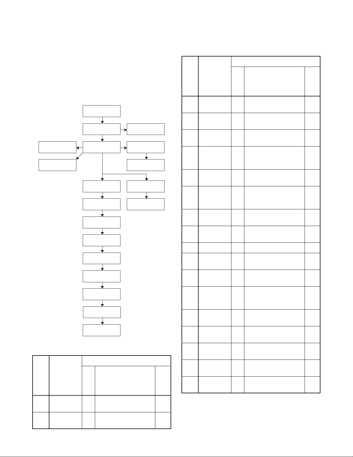
IMPORTANT SAFETY PRECAUTIONS
Prior to shipment from the factory, our products are strictly inspected for recognized product safety and electrical
codes of the countries in which they are to be sold. However, in order to maintain such compliance, it is equally
important to implement the following precautions when a set is being serviced.
Safety Precautions for LCD TV
Circuit
1. Before returning an instrument to the
customer, always make a safety check of the
entire instrument, including, but not limited to, the
following items:
a. Be sure that no built-in protective devices are
defective and have been defeated during
servicing. (1) Protective shields are provided
on this chassis to protect both the technician
and the customer. Correctly replace all missing
protective shields, including any removed for
servicing convenience. (2) When reinstalling
the chassis and/or other assembly in the
cabinet, be sure to put back in place all
protective devices, including but not limited to,
nonmetallic control knobs, insulating
fishpapers, adjustment and compartment
covers/shields, and isolation resistor/capacitor
networks. Do not operate this instrument or
permit it to be operated without all
protective devices correctly installed and
functioning. Servicers who defeat safety
features or fail to perform safety checks
may be liable for any resulting damage.
b. Be sure that there are no cabinet openings
through which an adult or child might be able to
insert their fingers and contact a hazardous
voltage. Such openings include, but are not
limited to, (1) spacing between the Liquid
Crystal Panel and the cabinet mask, (2)
excessively wide cabinet ventilation slots, and
(3) an improperly fitted and/or incorrectly
secured cabinet back cover.
c. Antenna Cold Check - With the instrument AC
plug removed from any AC source, connect an
electrical jumper across the two AC plug
prongs. Place the instrument AC switch in the
on position. Connect one lead of an ohmmeter
to the AC plug prongs tied together and touch
the other ohmmeter lead in turn to each tuner
antenna input exposed terminal screw and, if
applicable, to the coaxial connector. If the
measured resistance is less than 1.0 megohm
or greater than 5.2 megohm, an abnormality
exists that must be corrected before the
instrument is returned to the customer. Repeat
this test with the instrument AC switch in the off
position.
d. Leakage Current Hot Check - With the
instrument completely reassembled, plug the
AC line cord directly into a 120 V AC outlet. (Do
not use an isolation transformer during this
test.) Use a leakage current tester or a
metering system that complies with American
National Standards Institute (ANSI) C101.1
Leakage Current for Appliances and
Underwriters Laboratories (UL) 1410, (50.7).
With the instrument AC switch first in the on
position and then in the off position, measure
from a known earth ground (metal water pipe,
conduit, etc.) to all exposed metal parts of the
instrument (antennas, handle brackets, metal
cabinet, screw heads, metallic overlays, control
shafts, etc.), especially any exposed metal
parts that offer an electrical return path to the
chassis. Any current measured must not
exceed 0.5 milli-ampere. Reverse the
instrument power cord plug in the outlet and
repeat the test.
READING SHOULD
NOT BE ABOVE 0.5 mA
LEAKAGE
DEVICE
BEING
TESTED
TEST ALL EXPOSED
METAL SURFACES
ALSO TEST WITH
PLUG REVERSED
USING AC
ADAPTER PLUG
AS REQUIRED
ANY MEASUREMENTS NOT WITHIN THE
LIMITS SPECIFIED HEREIN INDICATE A
POTENTIAL SHOCK HAZARD THAT MUST
BE ELIMINATED BEFORE RETURNING THE
INSTRUMENT TO THE CUSTOMER OR
BEFORE CONNECTING THE ANTENNA OR
ACCESSORIES.
2. Read and comply with all caution and safety-
related notes on or inside the receiver cabinet, on
the receiver chassis, or on the Liquid Crystal
Panel.
CURRENT
TESTER
+
EARTH
GROUND
_
2-1 LTVN_ISP

3. Design Alteration Warning - Do not alter or add
to the mechanical or electrical design of this TV
receiver. Design alterations and additions,
including, but not limited to circuit modifications
and the addition of items such as auxiliary audio
and/or video output connections, might alter the
safety characteristics of this receiver and create a
hazard to the user. Any design alterations or
additions will void the manufacturer's warranty and
may make you, the servicer, responsible for
personal injury or property damage resulting
therefrom.
4. Hot Chassis Warning a. Some TV receiver chassis are electrically
connected directly to one conductor of the AC
power cord and maybe safety-serviced without
an isolation transformer only if the AC power
plug is inserted so that the chassis is
connected to the ground side of the AC power
source. To confirm that the AC power plug is
inserted correctly, with an AC voltmeter,
measure between the chassis and a known
earth ground. If a voltage reading in excess of
1.0 V is obtained, remove and reinsert the AC
power plug in the opposite polarity and again
measure the voltage potential between the
chassis and a known earth ground.
b. Some TV receiver chassis normally have 85V
AC(RMS) between chassis and earth ground
regardless of the AC plug polarity. This chassis
can be safety-serviced only with an isolation
transformer inserted in the power line between
the receiver and the AC power source, for both
personnel and test equipment protection.
c. Some TV receiver chassis have a secondary
ground system in addition to the main chassis
ground. This secondary ground system is not
isolated from the AC power line. The two
ground systems are electrically separated by
insulation material that must not be defeated or
altered.
5. Observe original lead dress. Take extra care to
assure correct lead dress in the following areas: a.
near sharp edges, b. near thermally hot parts-be
sure that leads and components do not touch
thermally hot parts, c. the AC supply, d. high
voltage, and, e. antenna wiring. Always inspect in
all areas for pinched, out of place, or frayed wiring.
Check AC power cord for damage.
6. Components, parts, and/or wiring that appear to
have overheated or are otherwise damaged
should be replaced with components, parts, or
wiring that meet original specifications.
Additionally, determine the cause of overheating
and/or damage and, if necessary, take corrective
action to remove any potential safety hazard.
7. Product Safety Notice - Some electrical and
mechanical parts have special safety-related
characteristics which are often not evident from
visual inspection, nor can the protection they give
necessarily be obtained by replacing them with
components rated for higher voltage, wattage, etc.
Parts that have special safety characteristics are
identified by a # on schematics and in parts lists.
Use of a substitute replacement that does not
have the same safety characteristics as the
recommended replacement part might create
shock, fire, and/or other hazards. The product's
safety is under review continuously and new
instructions are issued whenever appropriate.
Prior to shipment from the factory, our products
are strictly inspected to confirm they comply with
the recognized product safety and electrical codes
of the countries in which they are to be sold.
However, in order to maintain such compliance, it
is equally important to implement the following
precautions when a set is being serviced.
2-2 LTVN_ISP

Precautions during Servicing
A. Parts identified by the # symbol are critical for
safety.
Replace only with part number specified.
B. In addition to safety, other parts and assemblies
are specified for conformance with regulations
applying to spurious radiation. These must also be
replaced only with specified replacements.
Examples: RF converters, RF cables, noise
blocking capacitors, and noise blocking filters, etc.
C. Use specified internal wiring. Note especially:
1) Wires covered with PVC tubing
2) Double insulated wires
3) High voltage leads
D. Use specified insulating materials for hazardous
live parts. Note especially:
1) Insulation Tape
2) PVC tubing
3) Spacers
4) Insulators for transistors.
E. When replacing AC primary side components
(transformers, power cord, etc.), wrap ends of
wires securely about the terminals before
soldering.
F. Observe that the wires do not contact heat
producing parts (heat sinks, oxide metal film
resistors, fusible resistors, etc.)
G. Check that replaced wires do not contact sharp
edged or pointed parts.
H. When a power cord has been replaced, check that
5~6 kg of force in any direction will not loosen it.
I. Also check areas surrounding repaired locations.
J. Use care that foreign objects (screws, solder
droplets, etc.) do not remain inside the set.
K. When connecting or disconnecting the internal
connectors, first, disconnect the AC plug from the
AC supply outlet.
L. When installing parts or assembling the cabinet
parts, be sure to use the proper screws and
tighten certainly.
2-3 LTVN_ISP

Safety Check after Servicing
Examine the area surrounding the repaired location for damage or deterioration. Observe that screws, parts and
wires have been returned to original positions. Afterwards, perform the following tests and confirm the specified
values in order to verify compliance with safety standards.
1. Clearance Distance
When replacing primary circuit components, confirm
specified clearance distance (d) and (d') between
soldered terminals, and between terminals and
surrounding metallic parts. (See Fig. 1)
Table 1: Ratings for selected area
Chassis or Secondary Conductor
Primary Circuit
AC Line Voltage Region
110 to 130 V
Note: This table is unofficial and for reference only. Be
sure to confirm the precise values.
U.S.A. or
Canada
Clearance
Distance (d), (d’)
≥ 3.2 mm
(0.126 inches)
2. Leakage Current Test
Confirm the specified (or lower) leakage current
between B (earth ground, power cord plug prongs) and
externally exposed accessible parts (RF terminals,
antenna terminals, video and audio input and output
terminals, microphone jacks, earphone jacks, etc.) is
lower than or equal to the specified value in the table
below.
Measuring Method: (Power ON)
Insert load Z between B (earth ground, power cord plug
prongs) and exposed accessible parts. Use an AC
voltmeter to measure across both terminals of load Z.
See Fig. 2 and following table.
d' d
Fig. 1
Exposed Accessible Part
Z
AC Voltmeter
(High Impedance)
Earth Ground
B
Power Cord Plug Prongs
Fig. 2
Table 2: Leakage current ratings for selected areas
AC Line Voltage Region Load Z Leakage Current (i) Earth Ground (B) to:
110 to 130 V
Note: This table is unofficial and for reference only. Be sure to confirm the precise values.
U.S.A. or
Canada
0.15 µF CAP. & 1.5 kΩ
RES. Connected in parallel
2-4 LTVN_ISP
i ≤ 0.5 mA rms
Exposed accessible
parts

STANDARD NOTES FOR SERVICING
Circuit Board Indications
1. The output pin of the 3 pin Regulator ICs is
indicated as shown.
Top View
Out
2. For other ICs, pin 1 and every fifth pin are
indicated as shown.
Pin 1
3. The 1st pin of every male connector is indicated as
shown.
Pin 1
Input
In
Bottom View
5
10
Pb (Lead) Free Solder
Pb free mark will be found on PCBs which use Pb
free solder. (Refer to figure.) For PCBs with Pb free
mark, be sure to use Pb free solder. For PCBs
without Pb free mark, use standard solder.
Pb free mark
How to Remove / Install Flat Pack-IC
1. Removal
With Hot-Air Flat Pack-IC Desoldering Machine:
1. Prepare the hot-air flat pack-IC desoldering
machine, then apply hot air to the Flat Pack-IC
(about 5 to 6 seconds). (Fig. S-1-1)
Fig. S-1-1
2. Remove the flat pack-IC with tweezers while
applying the hot air.
3. Bottom of the flat pack-IC is fixed with glue to the
CBA; when removing entire flat pack-IC, first apply
soldering iron to center of the flat pack-IC and heat
up. Then remove (glue will be melted). (Fig. S-1-6)
4. Release the flat pack-IC from the CBA using
tweezers. (Fig. S-1-6)
CAUTION:
1. The Flat Pack-IC shape may differ by models. Use
an appropriate hot-air flat pack-IC desoldering
machine, whose shape matches that of the Flat
Pack-IC.
2. Do not supply hot air to the chip parts around the
flat pack-IC for over 6 seconds because damage
to the chip parts may occur. Put masking tape
around the flat pack-IC to protect other parts from
damage. (Fig. S-1-2)
3-1 TVN_SN

3. The flat pack-IC on the CBA is affixed with glue, so
be careful not to break or damage the foil of each
pin or the solder lands under the IC when
removing it.
With Soldering Iron:
1. Using desoldering braid, remove the solder from
all pins of the flat pack-IC. When you use solder
flux which is applied to all pins of the flat pack-IC,
you can remove it easily. (Fig. S-1-3)
CBA
Masking
Tape
Tweezers
Hot-air
Flat Pack-IC
Desoldering
Machine
Flat Pack-IC
Fig. S-1-2
Flat Pack-IC
Desoldering Braid
Soldering Iron
Fig. S-1-3
2. Lift each lead of the flat pack-IC upward one by
one, using a sharp pin or wire to which solder will
not adhere (iron wire). When heating the pins, use
a fine tip soldering iron or a hot air desoldering
machine. (Fig. S-1-4)
Sharp
Pin
Fine Tip
Soldering Iron
3. Bottom of the flat pack-IC is fixed with glue to the
CBA; when removing entire flat pack-IC, first apply
soldering iron to center of the flat pack-IC and heat
up. Then remove (glue will be melted). (Fig. S-1-6)
4. Release the flat pack-IC from the CBA using
tweezers. (Fig. S-1-6)
Fig. S-1-4
3-2 TVN_SN
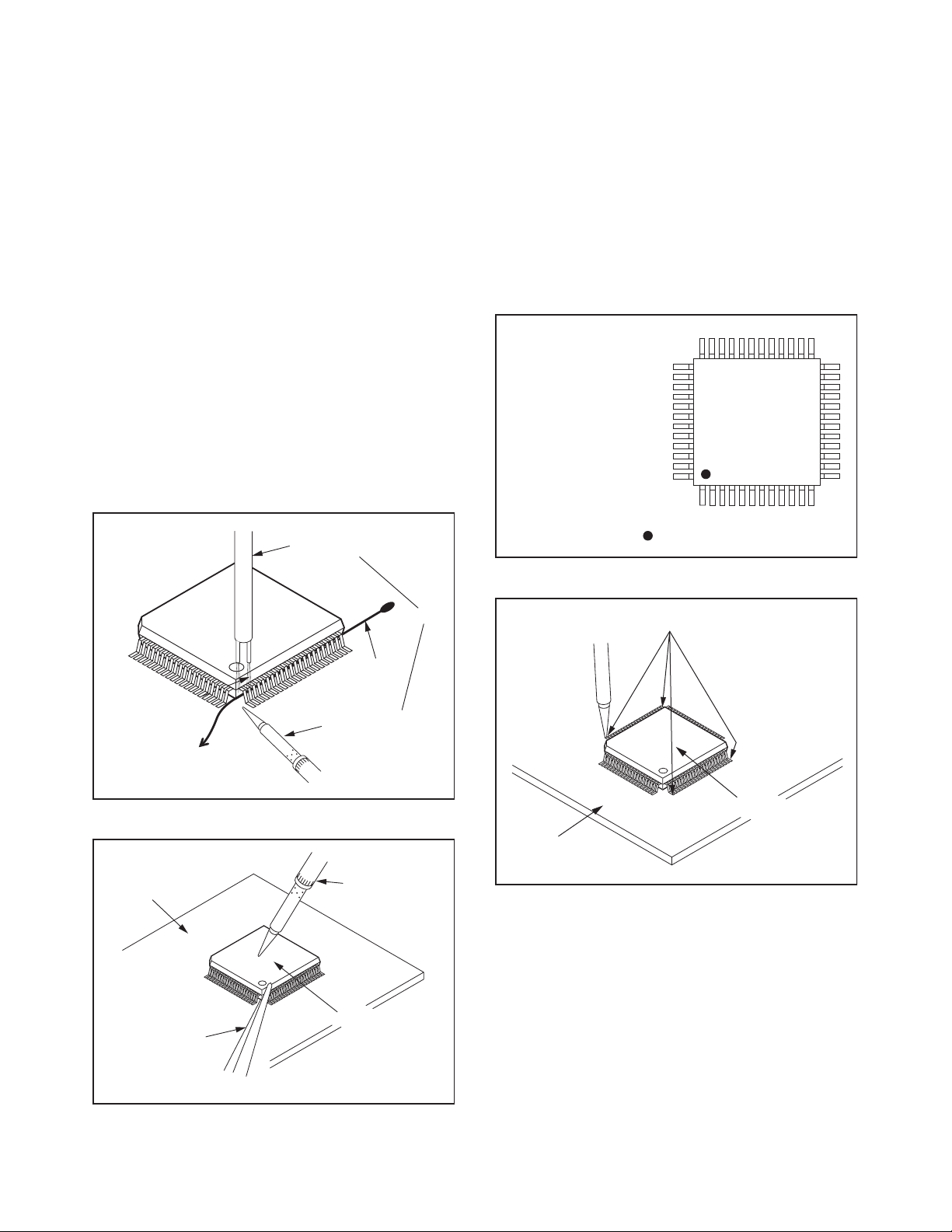
With Iron Wire:
1. Using desoldering braid, remove the solder from
all pins of the flat pack-IC. When you use solder
flux which is applied to all pins of the flat pack-IC,
you can remove it easily. (Fig. S-1-3)
2. Affix the wire to a workbench or solid mounting
point, as shown in Fig. S-1-5.
3. While heating the pins using a fine tip soldering
iron or hot air blower, pull up the wire as the solder
melts so as to lift the IC leads from the CBA
contact pads as shown in Fig. S-1-5.
4. Bottom of the flat pack-IC is fixed with glue to the
CBA; when removing entire flat pack-IC, first apply
soldering iron to center of the flat pack-IC and heat
up. Then remove (glue will be melted). (Fig. S-1-6)
5. Release the flat pack-IC from the CBA using
tweezers. (Fig. S-1-6)
Note: When using a soldering iron, care must be
taken to ensure that the flat pack-IC is not
being held by glue. When the flat pack-IC is
removed from the CBA, handle it gently
because it may be damaged if force is applied.
Hot Air Blower
2. Installation
1. Using desoldering braid, remove the solder from
the foil of each pin of the flat pack-IC on the CBA
so you can install a replacement flat pack-IC more
easily.
2. The “ I ” mark on the flat pack-IC indicates pin 1.
(See Fig. S-1-7.) Be sure this mark matches the
pin 1 on the PCB when positioning for installation.
Then presolder the four corners of the flat pack-IC.
(See Fig. S-1-8.)
3. Solder all pins of the flat pack-IC. Be sure that
none of the pins have solder bridges.
Example :
Pin 1 of the Flat Pack-IC
is indicated by a " " mark.
Fig. S-1-7
To Solid
Mounting Point
CBA
Tweezers
Iron Wire
Soldering Iron
Fig. S-1-5
Fine Tip
Soldering Iron
Flat Pack-IC
or
Presolder
Flat Pack-IC
CBA
Fig. S-1-8
Fig. S-1-6
3-3 TVN_SN

Instructions for Handling Semiconductors
Electrostatic breakdown of the semi-conductors may
occur due to a potential difference caused by
electrostatic charge during unpacking or repair work.
1. Ground for Human Body
Be sure to wear a grounding band (1 MΩ) that is
properly grounded to remove any static electricity that
may be charged on the body.
2. Ground for Workbench
Be sure to place a conductive sheet or copper plate
with proper grounding (1 MΩ) on the workbench or
other surface, where the semi-conductors are to be
placed. Because the static electricity charge on
clothing will not escape through the body grounding
band, be careful to avoid contacting semi-conductors
with your clothing.
<Incorrect>
<Correct>
1MΩ
CBA
Grounding Band
1MΩ
CBA
Conductive Sheet or
Copper Plate
3-4 TVN_SN
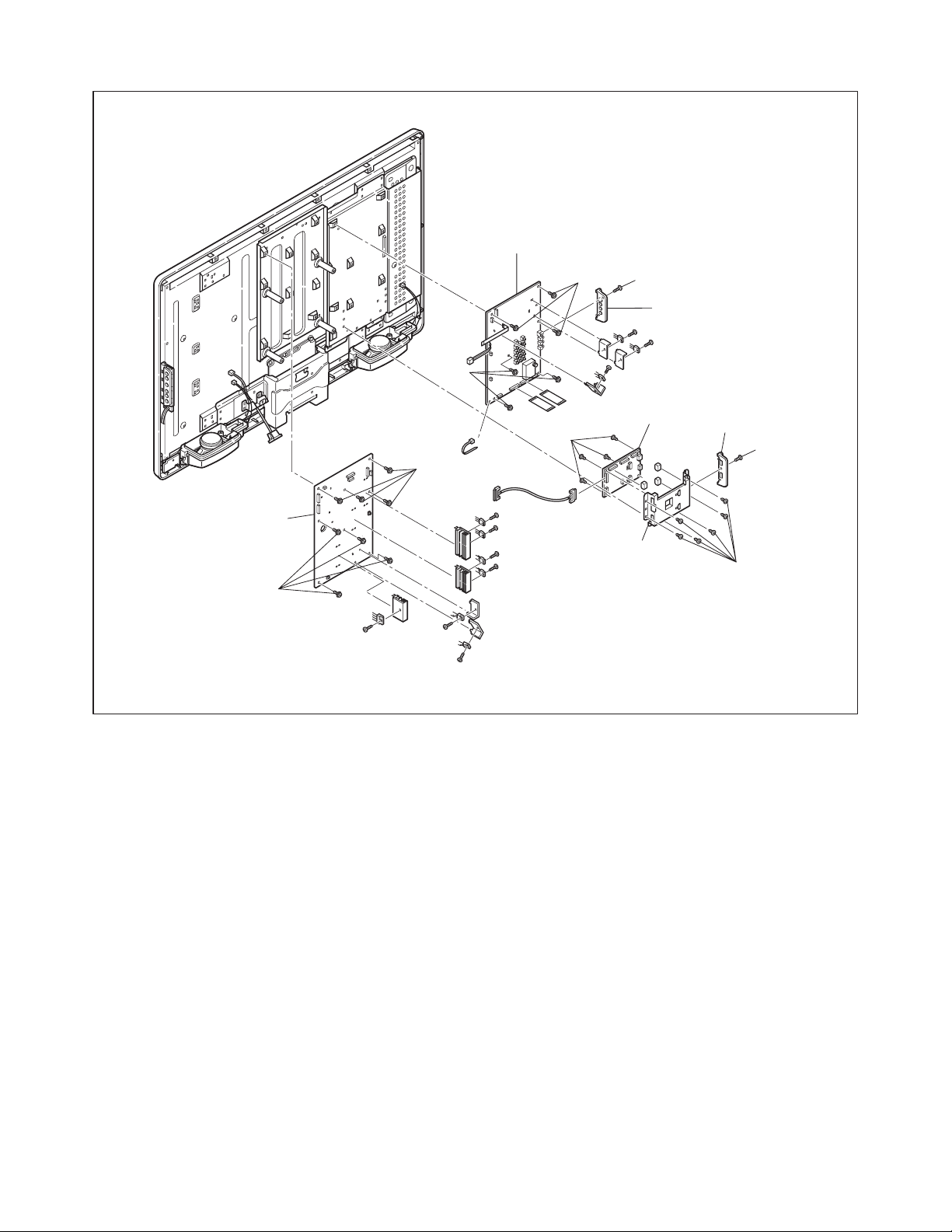
CABINET DISASSEMBLY INSTRUCTIONS
[42PFL3704D/F7(Serial No. : DS1A**********)]
1. Disassembly Flowchart
This flowchart indicates the disassembly steps for the
cabinet parts, and the CBA in order to gain access to
item(s) to be serviced. When reassembling, follow the
steps in reverse order. Bend, route and dress the
cables as they were.
[1] Stand
Assembly
[14] Junction
CBA
[15] Function
CBA
[2] Rear Cabinet
[3] Jack Holder
(D)
[4] Digital Main
CBA Unit
[5] Jack Holder
(A)
[6] Jack Power
CBA
[9] PCB Holder
[10] AC Inlet
Holder
[13] Speaker(s)
[16] IR Sensor
CBA
[7] Inverter
Power CBA
[8] Wall Mount
Bracket
Removal
Step/
Loc.
No.
Part
Fig.
Remove/*Unhook/
Unlock/Release/
No.
Unplug/Unclamp/
Desolder
Jack
[3]
Holder(D)
Digital Main
[4]
CBA UnitD2D5
Jack
[5]
Holder(A)
Jack Power
[6]
CBA
Inverter
[7]
Power CBAD2D5
Wall Mount
[8]
Bracket
D2 (S-7) ---
6(S-8), 4(S-9),
*CN201, *CN202,
*CN3901, Shield Box
D2 (S-10) ---
6(S-11), *CN203,
D2
*CN801, *CN802,
D5
*CN901, *CN1501
8(S-12), *CN1601,
*CN1803, *CN1804
D3 4(S-13) ---
[9] PCB Holder D3 4(S-14) ---
AC Inlet
[10]
[11]
Holder
Stand
Bracket
D3 2(S-15) ---
2(S-16), 2(S-17),
D3
4(S-18), 2(S-19)
LCD
[12]
Module
D4 6(S-20) ---
Assembly
Note
---
---
---
---
[11] Stand
Bracket
[12] LCD Module
Assembly
[17] Front
Cabinet
2. Disassembly Method
Removal
Step/
Loc.
No.
[1]
[2]
Part
Stand
Assembly
Rear
Cabinet
Remove/*Unhook/
Fig.
No.
Unlock/Release/
Unplug/Unclamp/
Desolder
D1 4(S-1) ---
11(S-2), 4(S-3),
D1
2(S-4), (S-5), (S-6)
4(S-21), 8(S-22),
Speaker Box(es)[F]
D4 Desolder ---
D4 *WH301A ---
D4 --------------- ---
D4 --------------- ---
↓
(3)
↓
(4)
Note
[13] Speaker(s) D4
Junction
[14]
CBA
Function
[15]
CBA
IR Sensor
[16]
CBA
Front
[17]
Cabinet
↓
(1)
↓
(2)
Note:
(1) Order of steps in procedure. When reassembling,
follow the steps in reverse order. These numbers
are also used as the Identification (location) No. of
---
parts in figures.
(2) Parts to be removed or installed.
4-1 A91H2DC
---
↓
(5)

(3) Fig. No. showing procedure of part location
(4) Identification of parts to be removed, unhooked,
unlocked, released, unplugged, unclamped, or
desoldered.
P = Spring, L = Locking Tab, S = Screw,
H = Hex Screw, CN = Connector
* = Unhook, Unlock, Release, Unplug, or Desolder
e.g. 2(S-2) = two Screws (S-2),
2(L-2) = two Locking Tabs (L-2)
(5) Refer to the following "Reference Notes in the
Ta bl e ."
(S-2)
[2] Rear Cabinet
(S-2)
[1] Stand Assembly
(S-1)
(S-3)
(S-2)
(S-5)
(S-6)
(S-2)
(S-4)
Fig. D1
4-2 A91H2DC

[6] Jack Power CBA
[7] Inverter
Power CBA
(S-12)
(S-11)
(S-12)
(S-9)
(S-11)
(S-10)
[5] Jack Holder(A)
[4] Digital Main
CBA Unit
Shield Box
[3] Jack Holder(D)
(S-7)
(S-8)
Fig. D2
4-3 A91H2DC

[11] Stand Bracket
(S-16)
(S-18)
[9] PCB Holder
[8] Wall Mount Bracket
(S-16)
(S-13)
(S-19)
(S-17)
(S-19)
(S-17)
(S-18)
[10] AC Inlet Holder
(S-14)
(S-15)
Fig. D3
4-4 A91H2DC
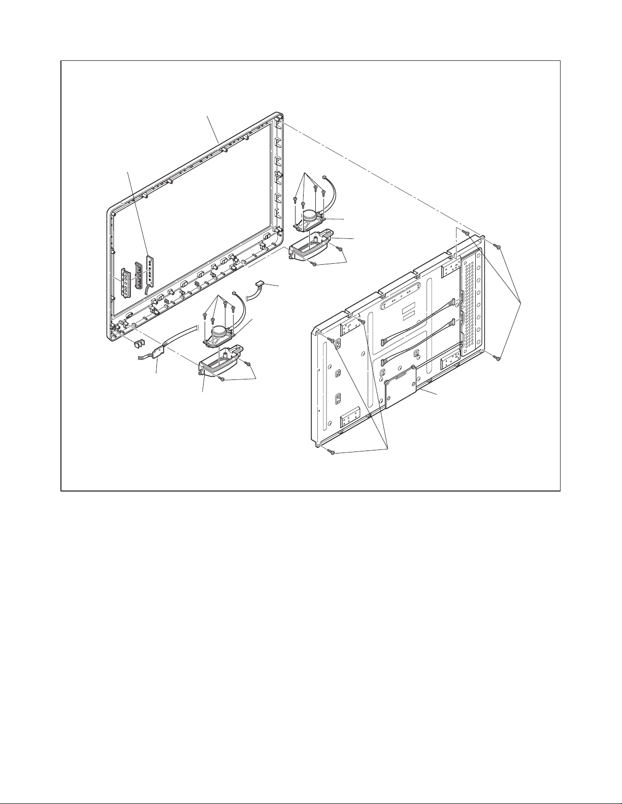
[17] Front Cabinet
[15] Function CBA
[16] IR Sensor
CBA
(S-22)
Speaker Box [F]
(S-22)
[14] Junction
CBA
[13] Speaker
(S-21)
[13] Speaker
Speaker Box [F]
(S-21)
(S-20)
[12] LCD Module
Assembly
(S-20)
Fig. D4
4-5 A91H2DC
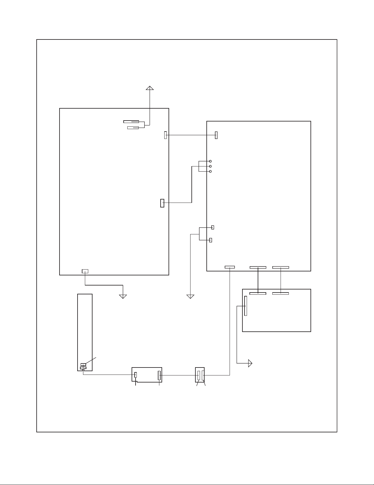
TV Cable Wiring Diagram
Inverter Power CBA
CN1803
CN1804
To LCD Module
Assembly
Jack Power CBA
Function
CBA
CN1601
To AC Inlet
CN1801
CN1501
To Speaker
CN901
CN601
CN801
CN802
CN203 CN202 CN201
CN3702 CN3701
CN3901
WH301A
IR Sensor CBA
WH302BWH301B CN302WH302A
Digital Main CBA Unit
Junction
CBA
To LCD Module
Assembly
Fig. D5
4-6 A91H2DC
CABINET DISASSEMBLY INSTRUCTIONS
[42PFL3704D/F7(Serial No. : YA1A**********)]
1. Disassembly Flowchart
This flowchart indicates the disassembly steps for the
cabinet parts, and the CBA in order to gain access to
item(s) to be serviced. When reassembling, follow the
steps in reverse order. Bend, route and dress the
cables as they were.
[1] Stand Base
Assembly
[3] Stand Sub
Cover
[15] Speaker(s)
[18] IR Sensor
CBA
[9] Inverter
Power CBA
[10] Wall Mount
Bracket
[16] Junction
CBA
[17] Function
CBA
[2] Stand Hinge
[4] Rear Cabinet
[5] Jack Holder
(D)
[6] Digital Main
CBA Unit
[7] Jack Holder
(A)
[8] Jack Power
CBA
Removal
Step/
Loc.
No.
Part
Fig.
Remove/*Unhook/
Unlock/Release/
No.
Unplug/Unclamp/
Note
Desolder
Stand Sub
[3]
Cover
Rear
[4]
Cabinet
Jack
[5]
Holder(D)
Digital Main
[6]
CBA UnitD2D5
Jack
[7]
Holder(A)
Jack Power
[8]
CBA
Inverter
[9]
Power CBAD2D5
Wall Mount
[10]
Bracket
D1 --------------- ---
11(S-4), 2(S-5), (S-6),
D1
(S-7)
D2 (S-8) ---
6(S-9), 4(S-10),
*CN201, *CN202,
*CN3901, Shield Box
D2 (S-11) ---
6(S-12), *CN203,
D2
*CN801, *CN802,
D5
*CN901, *CN1501
8(S-13), *CN1601,
*CN1803
D3 4(S-14) ---
[11] PCB Holder D3 4(S-15) ---
---
---
---
---
[11] PCB Holder
[12] AC Inlet
Holder
[13] Stand
Bracket
[14] LCD Module
Assembly
[19] Front
Cabinet
2. Disassembly Method
Removal
Step/
Loc.
No.
[1]
[2]
Part
Stand Base
Assembly
Stand
Hinge
Remove/*Unhook/
Fig.
No.
Unlock/Release/
Unplug/Unclamp/
Desolder
D1 4(S-1) ---
D1 4(S-2), 2(S-3) ---
Note
AC Inlet
[12]
[13]
Holder
Stand
Bracket
D3 2(S-16) ---
D3
LCD
[14]
Module
D4 6(S-20) ---
Assembly
[15] Speaker(s) D4
Junction
[16]
[17]
[18]
[19]
↓
(1)
CBA
Function
CBA
IR Sensor
CBA
Front
Cabinet
↓
(2)
D4 Desolder ---
D4 *WH301A ---
D4 (S-23) ---
D4 --------------- ---
↓
(3)
2(S-17), 2(S-18),
4(S-19)
4(S-21), 8(S-22),
Speaker Box(es)[F]
↓
(4)
---
---
↓
(5)
4-7 A91H5DC

Note:
(1) Order of steps in procedure. When reassembling,
follow the steps in reverse order. These numbers
are also used as the Identification (location) No. of
parts in figures.
(2) Parts to be removed or installed.
(3) Fig. No. showing procedure of part location
(4) Identification of parts to be removed, unhooked,
unlocked, released, unplugged, unclamped, or
desoldered.
P = Spring, L = Locking Tab, S = Screw,
H = Hex Screw, CN = Connector
* = Unhook, Unlock, Release, Unplug, or Desolder
e.g. 2(S-2) = two Screws (S-2),
2(L-2) = two Locking Tabs (L-2)
(5) Refer to the following "Reference Notes in the
Ta bl e ."
(S-4)
[4] Rear Cabinet
(S-4)
[1] Stand Base Assembly
(S-6)
(S-7)
(S-4)
(S-2)
[2] Stand Hinge
[3] Stand Sub Cover
(S-3)
(S-4)
(S-5)
(S-1)
Fig. D1
4-8 A91H5DC

[8] Jack Power CBA
[9] Inverter
Power CBA
(S-13)
(S-12)
(S-13)
(S-10)
(S-12)
(S-11)
[7] Jack Holder(A)
[6] Digital Main
CBA Unit
Shield Box
[5] Jack Holder(D)
(S-8)
(S-9)
Fig. D2
4-9 A91H5DC

(S-17)
(S-19)
[11] PCB Holder
[13] Stand Bracket
(S-17)
(S-18)
(S-19)
(S-15)
(S-18)
(S-16)
[10] Wall Mount Bracket
(S-14)
[12] AC Inlet Holder
Fig. D3
4-10 A91H5DC

[19] Front Cabinet
[17] Function CBA
[18] IR Sensor
CBA
(S-22)
(S-23)
Speaker Box [F]
(S-22)
[16] Junction
CBA
[15] Speaker
(S-21)
[15] Speaker
Speaker Box [F]
(S-21)
(S-20)
[14] LCD Module
Assembly
(S-20)
Fig. D4
4-11 A91H5DC

TV Cable Wiring Diagram
Inverter Power CBA
CN1803
To LCD Module
Assembly
Jack Power CBA
Function
CBA
CN1601
To AC Inlet
CN1801
CN1501
To Speaker
CN901
CN601
CN801
CN802
CN203 CN202 CN201
CN3702 CN3701
CN3901
WH301A
IR Sensor CBA
WH302BWH301B CN302WH302A
Digital Main CBA Unit
Junction
CBA
To LCD Module
Assembly
Fig. D5
4-12 A91H5DC

CABINET DISASSEMBLY INSTRUCTIONS
[42PFL3704D/F7(Serial No. : YA2A**********)]
1. Disassembly Flowchart
This flowchart indicates the disassembly steps for the
cabinet parts, and the CBA in order to gain access to
item(s) to be serviced. When reassembling, follow the
steps in reverse order. Bend, route and dress the
cables as they were.
[1] Stand Base
Assembly
[3] Stand Sub
Cover
[15] Speaker(s)
[18] IR Sensor
CBA
[9] Inverter
Power CBA
[10] Wall Mount
Bracket
[16] Junction
CBA
[17] Function
CBA
[2] Stand Hinge
[4] Rear Cabinet
[5] Jack Holder
(D)
[6] Digital Main
CBA Unit
[7] Jack Holder
(A)
[8] Jack Power
CBA
Removal
Step/
Loc.
No.
Part
Fig.
Remove/*Unhook/
Unlock/Release/
No.
Unplug/Unclamp/
Note
Desolder
Stand Sub
[3]
Cover
Rear
[4]
Cabinet
Jack
[5]
Holder(D)
Digital Main
[6]
CBA UnitD2D5
Jack
[7]
Holder(A)
Jack Power
[8]
CBA
Inverter
[9]
Power CBAD2D5
Wall Mount
[10]
Bracket
D1 --------------- ---
11(S-4), 2(S-5), (S-6),
D1
(S-7)
D2 (S-8) ---
6(S-9), 4(S-10),
*CN201, *CN202,
*CN3901, Shield Box
D2 (S-11) ---
6(S-12), *CN203,
D2
*CN801, *CN802,
D5
*CN901, *CN1501
8(S-13), *CN1601,
*CN1803, *CN1804
D3 4(S-14) ---
[11] PCB Holder D3 4(S-15) ---
---
---
---
---
[11] PCB Holder
[12] AC Inlet
Holder
[13] Stand
Bracket
[14] LCD Module
Assembly
[19] Front
Cabinet
2. Disassembly Method
Removal
Step/
Loc.
No.
[1]
[2]
Part
Stand Base
Assembly
Stand
Hinge
Remove/*Unhook/
Fig.
No.
Unlock/Release/
Unplug/Unclamp/
Desolder
D1 4(S-1) ---
D1 4(S-2), 2(S-3) ---
Note
AC Inlet
[12]
[13]
Holder
Stand
Bracket
D3 2(S-16) ---
D3
LCD
[14]
Module
D4 6(S-20) ---
Assembly
[15] Speaker(s) D4
Junction
[16]
[17]
[18]
[19]
↓
(1)
CBA
Function
CBA
IR Sensor
CBA
Front
Cabinet
↓
(2)
D4 Desolder ---
D4 *WH301A ---
D4 (S-23) ---
D4 --------------- ---
↓
(3)
2(S-17), 2(S-18),
4(S-19)
4(S-21), 8(S-22),
Speaker Box(es)[F]
↓
(4)
---
---
↓
(5)
4-13 A91H9DC

Note:
(1) Order of steps in procedure. When reassembling,
follow the steps in reverse order. These numbers
are also used as the Identification (location) No. of
parts in figures.
(2) Parts to be removed or installed.
(3) Fig. No. showing procedure of part location
(4) Identification of parts to be removed, unhooked,
unlocked, released, unplugged, unclamped, or
desoldered.
P = Spring, L = Locking Tab, S = Screw,
H = Hex Screw, CN = Connector
* = Unhook, Unlock, Release, Unplug, or Desolder
e.g. 2(S-2) = two Screws (S-2),
2(L-2) = two Locking Tabs (L-2)
(5) Refer to the following "Reference Notes in the
Ta bl e ."
(S-4)
[4] Rear Cabinet
(S-4)
[1] Stand Base Assembly
(S-6)
(S-7)
(S-4)
(S-2)
[2] Stand Hinge
[3] Stand Sub Cover
(S-3)
(S-4)
(S-5)
(S-1)
Fig. D1
4-14 A91H9DC
[8] Jack Power CBA
[9] Inverter
Power CBA
(S-13)
(S-12)
(S-13)
(S-10)
(S-12)
(S-11)
[7] Jack Holder(A)
[6] Digital Main
CBA Unit
Shield Box
[5] Jack Holder(D)
(S-8)
(S-9)
Fig. D2
4-15 A91H9DC

(S-17)
(S-19)
[11] PCB Holder
[13] Stand Bracket
(S-17)
(S-18)
(S-19)
(S-15)
(S-18)
(S-16)
[10] Wall Mount Bracket
(S-14)
[12] AC Inlet Holder
Fig. D3
4-16 A91H9DC

[19] Front Cabinet
[17] Function CBA
[18] IR Sensor
CBA
(S-22)
(S-23)
Speaker Box [F]
(S-22)
[16] Junction
CBA
[15] Speaker
(S-21)
[15] Speaker
Speaker Box [F]
(S-21)
(S-20)
[14] LCD Module
Assembly
(S-20)
Fig. D4
4-17 A91H9DC

TV Cable Wiring Diagram
Inverter Power CBA
CN1803
CN1804
To LCD Module
Assembly
Jack Power CBA
Function
CBA
CN1601
To AC Inlet
CN1801
CN1501
To Speaker
CN901
CN601
CN801
CN802
CN203 CN202 CN201
CN3702 CN3701
CN3901
WH301A
IR Sensor CBA
WH302BWH301B CN302WH302A
Digital Main CBA Unit
Junction
CBA
To LCD Module
Assembly
Fig. D5
4-18 A91H9DC
 Loading...