

Philips FB2033BB Datasheet

INTEGRATED CIRCUITS
FB2033
8-bit latched/registered/pass-thru
Futurebus+ universal interface transceiver
Product specification
IC19 Data Handbook
1995 May 25
Philips Semiconductors Product specification
I
S
t
A
8-bit latched/registered/pass-thru
Futurebus+ universal interface transceiver
FEA TURES
•8-bit transceivers
•Latched, registered or straight through in either A to B or B to A
path
•Drives heavily loaded backplanes with equivalent load
impedances down to 10Ω.
•High drive 100mA BTL Open Collector drivers on B-port
•Allows incident wave switching in heavily loaded backplane buses
•Reduced BTL voltage swing produces less noise and reduces
power consumption
QUICK REFERENCE DATA
SYMBOL PARAMETER TYPICAL UNIT
t
PLH
t
PHL
t
PLH
t
PHL
C
I
OB
OL
CC
Propagation delay
AIn to Bn
Propagation delay
Bn to AOn
Output capacitance (B0 – Bn only) 6 pF
Output current (B0 – Bn only) 100 mA
AIn to Bn
upply curren
(outputs Low or High)
Bn to AOn (outputs Low) 45
Bn to AOn (outputs High) 22
FB2033
•Built-in precision band-gap reference provides accurate receiver
thresholds and improved noise immunity
•Compatible with IEEE Futurebus+ or proprietary BTL backplanes
•Each BTL driver has a dedicated Bus GND for a signal return
•Controlled output ramp and multiple GND pins minimize ground
bounce
•Glitch-free power up/power down operation
•Low I
•Tight output skew
•Supports live insertion
current
CC
3.0
3.0
4.3
4.1
24
ns
ns
m
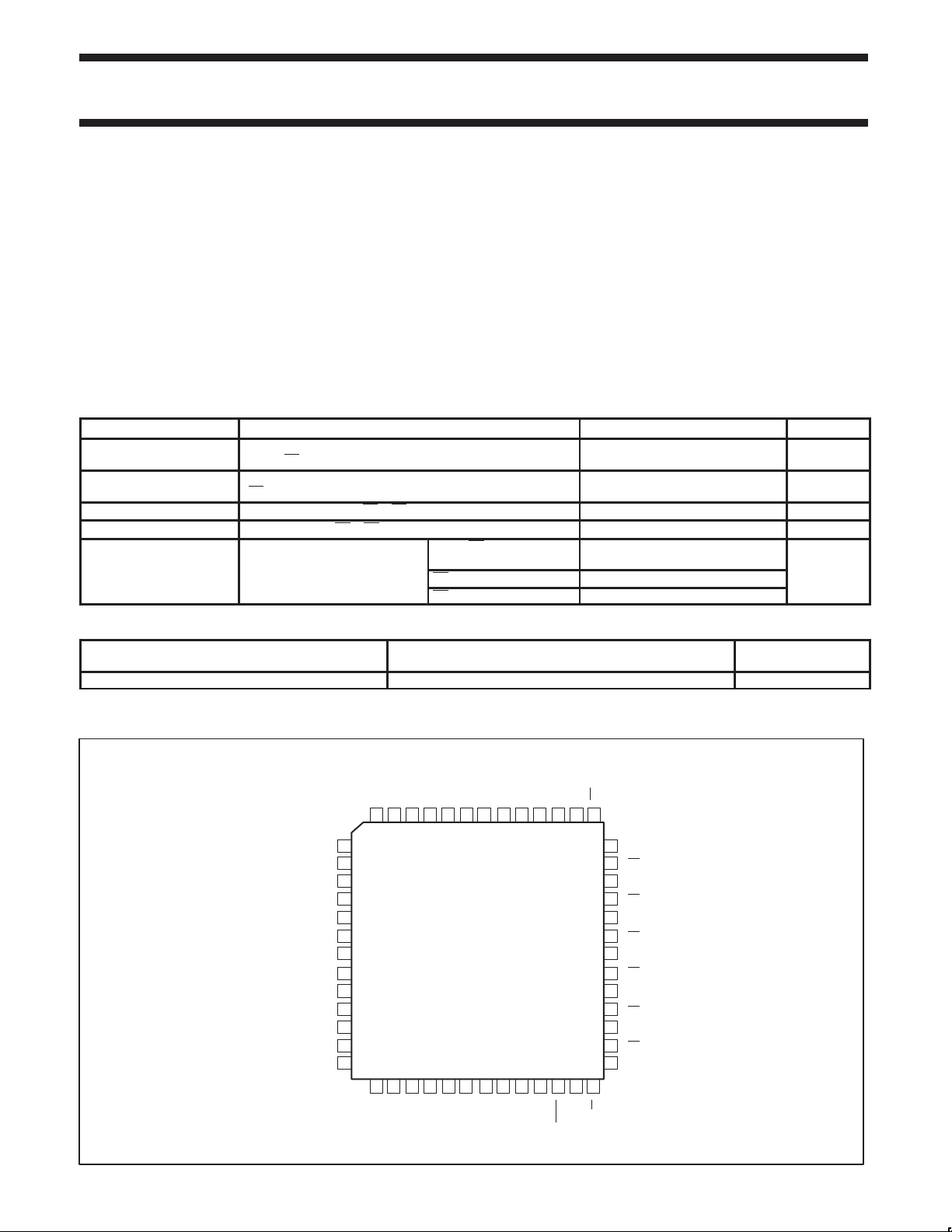
ORDERING INFORMATION
PACKAGES
52-pin Plastic Quad Flat Pack (QFP) FB2033BB SOT379-1
NOTE: Thermal mounting or forced air is recommended
PIN CONFIGURATION
52 51 50 49 48 47 46 45 44 43 42 41 40
LOGIC GND
LOOPBACK
LOGIC GND
AO1
AI2
AO2
AI3
AO3
AI4
AO4
AI5
AO5
AI6
1
2
3
4
5
6
7
8
9
10
11
12
13
14 15 16 17 18 19 20 21 22 23 24 25 26
COMMERCIAL RANGE
VCC = 5V±10%; T
AO0
LOGIC GND
AI0
LCAB
SBA1
AI1
CC
V
8-Bit Universal Transceiver
FB2033
52-lead PQFP
AO7
LGOIC GND
CC
V
SAB0
LCBA
AO6
AI7
SBA0
SAB1
CC
BG V
CC
V
= 0°C to +70°C
amb
OEA
BIAS V
BG GND
OEB0
OEB1
BUS GND
B0
B7
39
38
37
36
35
34
33
32
31
30
29
28
27
DRAWING
NUMBER
BUS GND
B1
BUS GND
B2
BUS GND
B3
BUS GND
B4
BUS GND
B5
BUS GND
B6
BUS GND
SG00068
1995 May 25 853-1717 15279
2

Philips Semiconductors Product specification
8-bit latched/registered/pass-thru
Futurebus+ universal interface transceiver
DESCRIPTION
The FB2033 is an 8-bit transceiver featuring a split input (AI) and
output (AO) bus on the TTL-level side.
The common I/O, open collector B port operates at BTL signal
levels. The logic element for data flow in each direction is controlled
by two pairs of mode select inputs (SBA0 and SBA1 for B-to-A,
SAB0 and SAB1 for A-to-B). It can be configured as a buffer, a
register, or a D-type latch.
When configured in the buffer mode, the inverse of the input data
appears at the output port. In the flip-flop mode, data is stored on
the rising edge of the appropriate clock input (LCAB or LCBA). In the
latch mode, clock pins serve as transparent-High latch enables.
Regardless of the mode, data is inverted from input to output.
Data flow in the B-to-A direction, regardless of the logic element
selected, is further controlled by the Loopback input. When the
Loopback input is High the output of the selected A-to-B logic
element (not inverted) becomes the B-to-A input.
The 3-State AO port is enabled by asserting a High level on OEA.
The B port has two output enables, OEB0 and OEB1
OEB0 is High and OEB1
OEB0 is Low or OEB1
the level of the pull-up voltage. New data can be entered in the
flip-flop and latched modes or can be retained while the associated
outputs are in 3-State (AO port) or inactive (B port).
The B-port drivers are Low-capacitance open collectors with
controlled ramp and are designed to sink 100mA. Precision band
gap references on the B-port ensure very good noise margins by
limiting the switching threshold to a narrow region centered at 1.55V .
The B-port interfaces to “Backplane Transceiver Logic” (see the
IEEE 1194.1 BTL standard). BTL features low power consumption
is Low is the output enabled. When either
is High, the B-port is inactive and is pulled to
. Only when
FB2033
by reducing voltage swing (1V p-p, between 1V and 2V) and
reduced capacitive loading by placing an internal series diode on the
drivers. BTL also provides incident wave switching, a necessity for
high performance backplanes.
Output clamps are provided on the BTL outputs to further reduce
switching noise. The “V
during a Low-to-High transition. The “V
The other clamp, the “trapped reflection” clamp, clamps out ringing
below the BTL 0.5V V
approximately 100ns after a High-to-Low transition.
To support live insertion, OEB0 is held Low during power on/off
cycles to ensure glitch- free B port drivers. Proper bias for B port
drivers during live insertion is provided by the BIAS V pin when at a
5V level while V
which will reverse-bias the BTL driver series Schottky diode, and
also bias the B port output pins to a voltage between 1.62V and
2.1V. This bias function is in accordance with IEEE BTL Standard
1194.1. If live insertion is not a requirement, the BIAS V pin should
be tied to a V
The LOGIC GND and BUS GND pins are isolated inside the
package to minimize noise coupling between the BTL and TTL
sides. These pins should be tied to a common ground external to the
package.
Each BTL driver has an associated BUS GND pin that acts as a
signal return path and these BUS GND pins are internally isolated
from each other. In the event of a ground return fault, a “hard” signal
failure occurs instead of a pattern dependent error that may be very
infrequent and impossible to trouble- shoot.
As with any high power device thermal considerations are critical. It
is recommended that airflow (300Ifpm) and/or thermal mounting be
used to ensure proper junction temperature.
CC
CC
pin.
” clamp reduces inductive ringing effects
OH
level. This clamp remains active for
OL
is Low. The BIAS V pin is a low current input
” clamp is always active.
OH
PIN DESCRIPTION
SYMBOL PIN NUMBER TYPE NAME AND FUNCTION
AI0 – AI7 50, 52, 3, 5, 8, 10, 12, 15 Input Data inputs (TTL)
AO0 – AO7 51, 2, 4, 6, 9, 11, 14, 16 Output 3-State outputs (TTL)
B0 – B7 40, 38, 36, 34, 32, 30, 28, 26 I/O Data inputs/Open Collector outputs, High current drive (BTL)
OEB0 23 Input Enables the B outputs when High
OEB1 24 Input Enables the B outputs when Low
OEA 43 Input Enables the AO outputs when High
BUS GND 39, 37, 35, 33, 31, 29, 27, 25 GND Bus ground (0V)
LOGIC GND 1, 13, 17, 49 GND Logic ground (0V)
V
CC
BIAS V 41 Power Live insertion pre-bias pin
BG V
CC
BG GND 42 GND Band Gap threshold voltage reference ground
SABn 20, 21 Input Mode select from AI to B
SBAn 45, 46 Input Mode select from B to AO
LCAB 47 Input A-to-B clock/latch enable (transparent latch when High)
LCBA 19 Input B-to-A clock/latch enable (transparent latch when High)
Loopback 7 Input Enables loopback function when High (from AIn to AOn)
18, 22, 48 Power Positive supply voltage
44 Power Band Gap threshold voltage reference
1995 May 25
3
Philips Semiconductors Product specification
AIn to Bn thru mode
AIn to Bn transparent latch
AIn to Bn latch and read
AIn to Bn register
Bn to AOn thru mode
Bn to AOn transparent latch
Bn to AOn latch and read
Bn to AOn register
Disable Bn outputs
8-bit latched/registered/pass-thru
FB2033
Futurebus+ universal interface transceiver
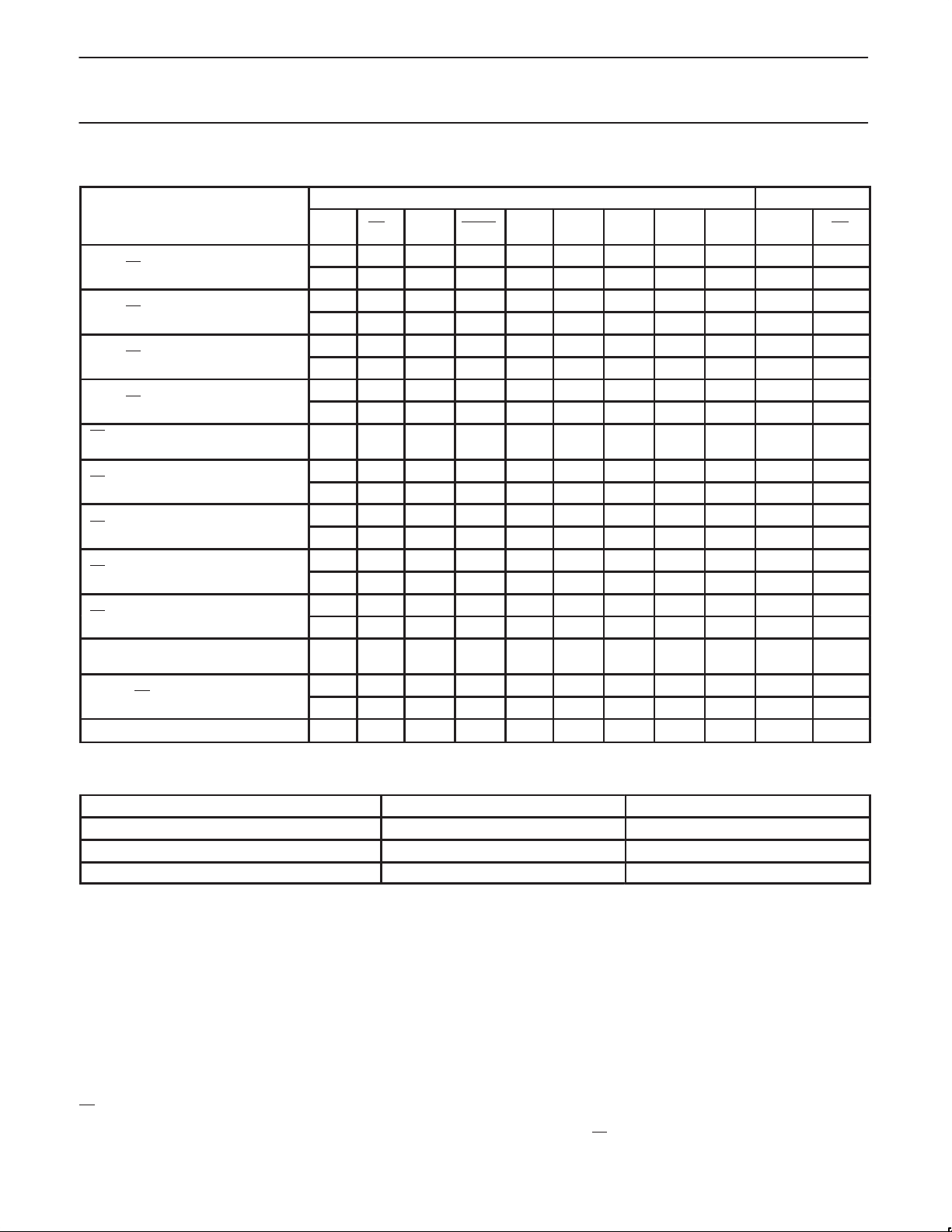
FUNCTION TABLE
INPUTS OUTPUTS
MODE
p
Bn outputs latched and read
(preconditioned latch)
p
AOn outputs latched and read
(preconditioned latch)
p
Disable AOn outputs X X X X L X X XX XX Z X
AIn Bn* OEB0 OEB1 OEA LCAB LCBA
L — H L L X X LL XX Z H**
H — H L L X X LL XX Z L
L — H L L H X HX XX Z H**
H — H L L H X HX XX Z L
l — H L L ↓ X HX XX Z H**
h — H L L ↓ X HX XX Z L
L — H L L ↑ X LH XX Z H**
H — H L L ↑ X LH XX Z L
X — H L L L X HX XX Z
X L L H H X X XX LL H input
X H L H H X X XX LL L input
X L L H H X H XX HX H input
X H L H H X H XX HX L input
X l L H H X ↓ XX HX H input
X h L H H X ↓ XX HX L input
X L L H H X ↑ XX LH H input
X H L H H X ↑ XX LH L input
X X L H H X L XX HX
X X L X X X X XX XX X H**
X X X H X X X XX XX X H**
SAB
0
SBA
1
1
0
AOn Bn
latched
data
latched
data
X
FUNCTION SELECT TABLE
NOTES:
H = High voltage level
L = Low voltage level
h = High voltage level one set-up time prior to the High-to-Low LCXX transition
l = Low voltage level one set-up time prior to the High-to-Low LCXX transition
X = Don’t care
Z = High-impedance (OFF) state
— = Input not externally driven
↑ = Low-to-High transition
↓ = High-to-Low transition
H** = Goes to level of pull-up voltage
* = Precaution should be taken to ensure B inputs do not float. If they do, they are equal to Low state.
Bn
NOTE: In Loopback mode (Loopback = High), AIn inputs are routed to the AOn outputs. The Bn
1995 May 25
MODE SELECTED SXX1 SXX0
Thru mode L L
Register mode L H
Latch mode H X
inputs are blocked out.
4
Philips Semiconductors Product specification
8-bit latched/registered/pass-thru
Futurebus+ universal interface transceiver
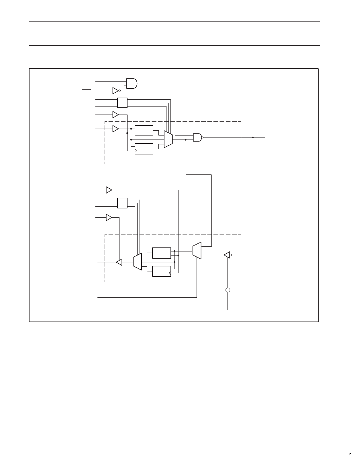
LOGIC DIAGRAM
23
OEB0
24
OEB1
20
SAB0
21
SAB1
47
LCAB
50
AIn
LCBA
SBA0
SBA1
OEA
52,
2, 5,
8, 10,
12, 15
1 of 8 cells
19
45
46
43
D
En
D
Clk
40
36, 34,
32, 30,
FB2033
Bn
38,
28, 26
AOn
2, 4, 6, 9,
11, 14, 16
Loopback
51
7
1 of 8 cells
D
En
D
Clk
BGGnd
BGref
42
SG00069
1995 May 25
5
 Loading...