

Page 1
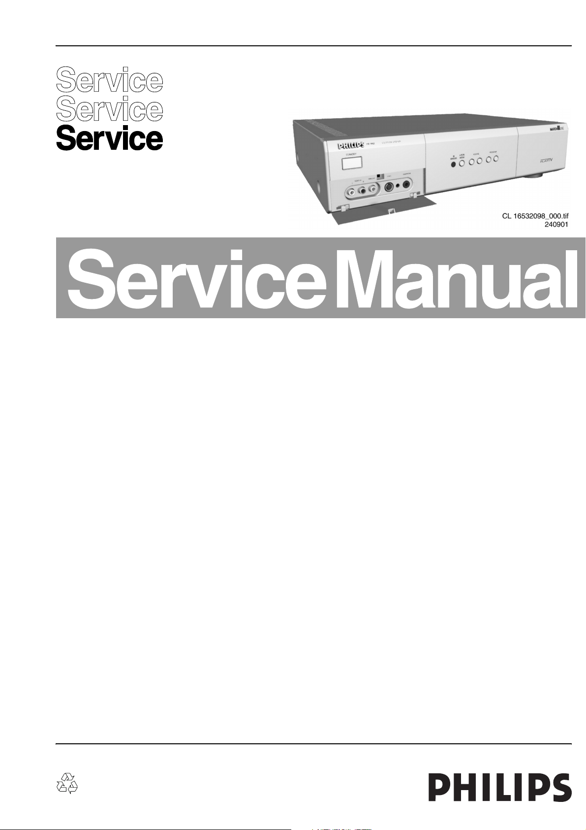
Colour Television Chassis
F21RE
AB
Contents Page Contents Page
1 Technical Specifications, Connection Facilities,
and Chassis Overview 2
2 Safety Instructions, Maintenance, 6
Warnings, and Notes
3 Directions for Use 7
4 Mechanical Instructions 26
5 Service Modes, Error Codes, 29
Faultfinding, and Repair Tips.
6 Block Diagrams
Block Diagram (Video) 37
Block Diagram (Audio + Supply) 38
Powerlines Overview 39
2
I
C IC’s Overview 40
Testpoint Overviews (AV + PS) 41
Testpoint Overviews (K + L + M) 42
Wiring Diagram 43
7 Electrical Diagrams and PWB lay-outs Diagram PWB
AVI: Connections (Diagram AV1) 44 52-54
AVI: HD-Matrix / Sync Remover(Diagram AV2) 45 46-48
AVI: Sync Processing (Diagram AV3) 46 46-48
AVI: VGA / HD-Selection (Diagram AV4) 47 46-48
AVI: Output + Select. Supply (Diagram AV5) 48 46-48
AVI: YPbPr-RGB Matrix (Diagram AV6) 49 46-48
AVI: Video + RC-Selection (Diagram AV7) 50 46-48
AVI: Audio + Control (Diagram AV8) 51 46-48
2D Comb Filter Add-on (Diagram CF) 55 55
Front Panel (Diagram FP1) 56 57
SSB: Tuner, IF, Sourse Select and Video
Processing (Diagram K1) 58 65-70
SSB: Input/Output (Diagram K2) 59 65-70
SSB: Sound Processing (Diagram K3) 60 65-70
SSB: Audio Dolby (Diagram K4) 61 65-70
SSB: Video Control+ Geometry (Diagram K6) 62 65-70
SSB: TXT + Control (Diagram K7) 63 65-70
©
Copyright 2003 Philips Consumer Electronics B.V. Eindhoven, The Netherlands.
All rights reserved. No part of this publication may be reproduced, stored in a
retrieval system or transmitted, in any form or by any means, electronic,
mechanical, photocopying, or otherwise without the prior permission of Philips.
SSB: Source Sel. (add to K1) (Diagram K8) 64 65-70
Feature Box 7: Feature Box (Diagram L1) 71 74-75
Feature Box 7: Eagle (NA) (Diagram L2) 72 74-75
Feature Box 7: Falconic (Diagram L3) 73 74-75
Power Supply (Diagram PS) 76 77-78
SD Connector Panel (Diagram SD) 79 80
8 Electrical Alignments 81
9 Circuit Descriptions 87
List of Abbreviations 99
IC-Data 101
10 Spare Parts List 107
11 Revision List 114
Published by WO 0364 Service PaCE Printed in the Netherlands Subject to modification EN 3122 785 13130
Page 2
EN 2 F21RE AB1.
Technical Specifications, Connections, and Chassis Overview
1. Technical Specifications, Connections, and Chassis Overview
1.1 Technical Specifications
1.1.1 Reception
Tuning system : PLL
Colour systems : PAL B/G, D/K, I
Sound systems : FM/AM-mono
A/V connections : PAL B/G, D/K, I
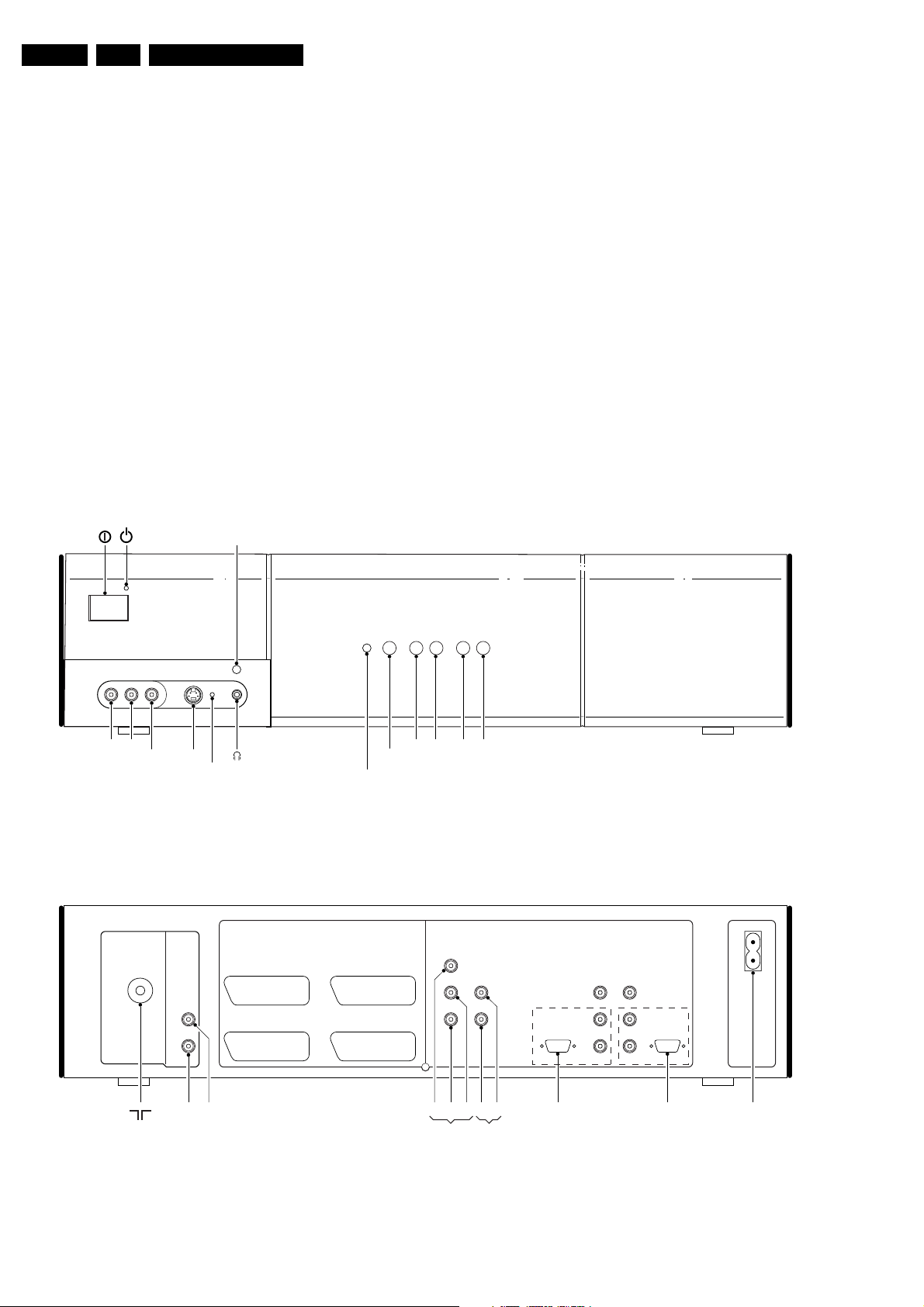
1.2 Connections
1.2.1 Front Connections
RedPower
Service IR-Receiver
: SECAM B/G, D/K
L/L1
: FM/FM B/G, Czech
: NICAM B/G, D/K, I, L
: SECAM B/G, D/K,
L/L1
: NTSC 4.43 (playback
only)
FRONT VIEW
Channel selections : 125 channels
: Full cable, UVSH
Aerial input : 75 Ohm, IEC-type
1.1.2 Miscellaneous
Mains voltage : 95 - 264 Vac
Mains frequency : 50 - 60 Hz
Ambient temperature : + 5 to + 45 deg. C
Maximum humidity : 90% R.H.
Power ON dissipation : 28 W typical
Power OFF dissipation : 0.2 W typical
Standby Power dissipation : 0.6 W Typical
Weight : 4 kg
Dimensions (WxHxD) : 435 x 100 x 330 mm
L
Audio
In
R
Video
S-VHS in
In
Service-IR
Send LED
IR-Receiver
-+ -+
Local
Volume
Menu
Program
REAR VIEW
R
L
Audio out
EXTERNAL 3
EXTERNAL 1
EXTERNAL 4
EXTERNAL 2
RLPrYPb
Video Audio
External 5
Figure 1-1 Front and rear connections
Center In
PC/MAC
In
VGA1-in
(15p)
No Function
L
R
L
Monitor
R
VGA2-out
(15p)
out
Mains
~
CL 16532098_004.eps
240901
Page 3
Technical Specifications, Connections, and Chassis Overview
EN 3F21RE AB 1.
Audio/Video - In
1 - Audio L 2.5 V_rms/33 kOhm
2 - Audio R 2.5 V_rms/33 kOhm
3 - Video CVBS 1 V_pp/75 Ohm
4 - Headphone 100 mW/8 Ohm
15mW/2 kOhm
SVHS - In
1 - Y Ground
2 - C Ground
3 - Y 1 V_pp/75 Ohm
4 - C 0.3 V_pp/75 Ohm
1.2.2 Rear Connections
Aerial - In
1 - IEC-type Coax, 75 Ohm
Audio - Out (Constant Level)
1 - Audio L 0.5 V_rms/10 kOhm
2 - Audio R 0.5 V_rms/10 kOhm
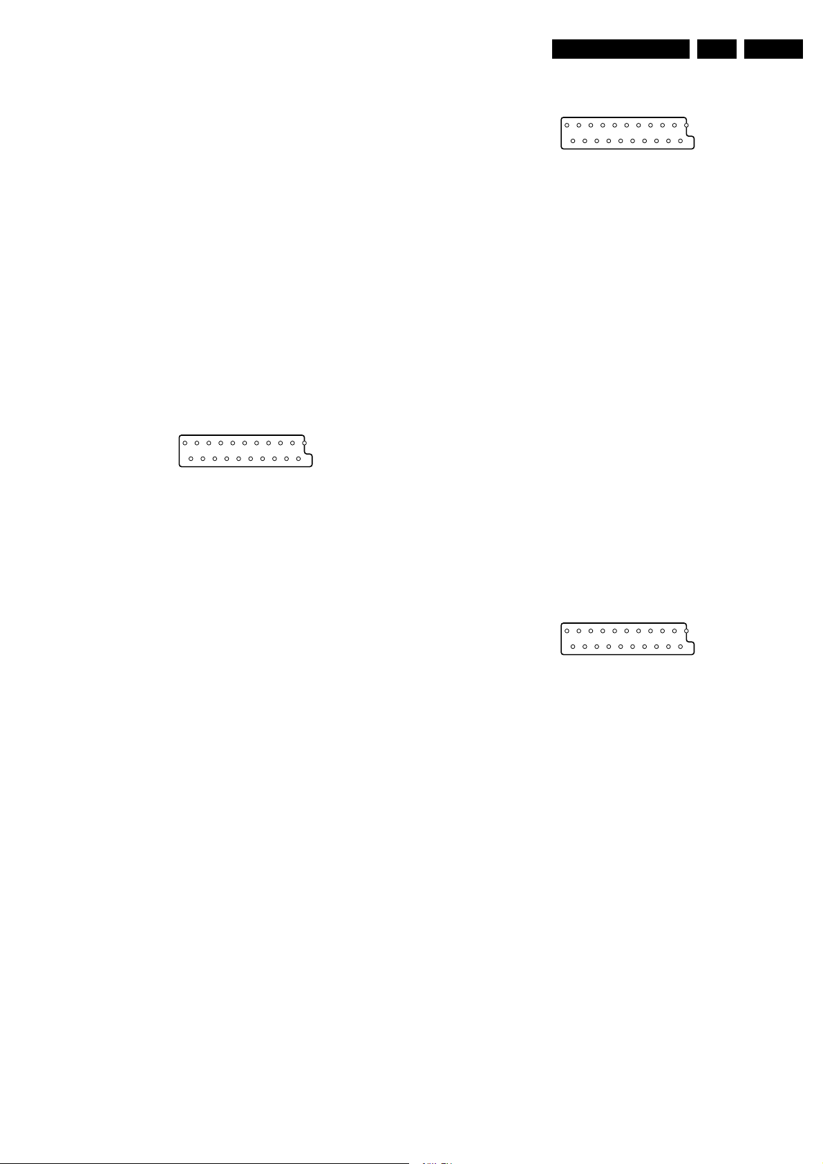
EXT1: SCART - In/Out (RGB, CVBS)
121
CL96532137_056.eps
202
171199
Figure 1-2 SCART connector
1 - Audio - R 0.5 V_rms/1 kOhm
2 - Audio - R 0.5 V_rms/10 kOhm
3 - Audio - L 0.5 V_rms/1 kOhm
4 - Audio Ground
5 - Blue Ground
6 - Audio - L 0.5 V_rms/10 kOhm
7 - Blue 0.7 V_pp/75 Ohm
8 - CVBS-status 0 - 1.3 V: INT
4.5 - 7 V: EXT 16:9
9.5 - 12 V: EXT 4:3
9 - Green Ground
10 -
11 - Green 0.7 V_pp/75 Ohm
12 -
13 - Red Ground
14 - RGB-status Ground
15 - Red 0.7 V_pp/75 Ohm
16 - RGB-stat./FBL 0 - 0.4 V: INT
1 - 3 V: EXT/75 Ohm
17 - CVBS Ground
18 - FBL Ground
19 - CVBS 1 V_pp/75 Ohm
20 - CVBS 1 V_pp/75 Ohm
21 - Shielding Ground
EXT2: SCART - In/Out for VCR (RGB, CVBS, SVHS)
121
CL96532137_056.eps
202
171199
Figure 1-3 SCART connector
1 - Audio - R 0.5 V_rms/1 kOhm
2 - Audio - R 0.5 V_rms/10 kOhm
3 - Audio - L 0.5 V_rms/1 kOhm
4 - Audio Ground
5 - Blue Ground
6 - Audio - L 0.5 V_rms/10 kOhm
7 - Blue/C 0.7 V_pp/75 Ohm
8 - CVBS-status 0 - 1.3 V: INT
4.5 - 7 V: EXT 16:9
9.5 - 12 V: EXT 4:3
9 - Green Ground
10 - Easy Link (P50)
11 - Green 0.7 V_pp/75 Ohm
12 -
13 - Red Ground
14 - RGB-status Ground
15 - Red/C 0.7 V_pp/75 Ohm
16 - RGB-stat./FBL 0 - 0.4 V: INT
1 - 3 V: EXT/75 Ohm
17 - CVBS Ground
18 - FBL Ground
19 - Y/CVBS 1 V_pp/75 Ohm
20 - Y/CVBS 1 V_pp/75 Ohm
21 - Shielding Ground
EXT3: SCART - In (CVBS, Audio)
121
CL96532137_056.eps
202
171199
Figure 1-4 SCART connector
1-
2 - Audio - R 0.5 V_rms/10 kOhm
3-
4 - Audio Ground
5 - Ground
6 - Audio - L 0.5 V_rms/10 kOhm
7-
8 - CVBS-status 0 - 1.3 V: INT
4.5 - 7 V: EXT 16:9
9.5 - 12 V: EXT 4:3
9 - Ground
10 -
11 -
12 -
13 - Ground
14 - Status Ground
15 -
16 -
17 - CVBS Ground
18 - CVBS Ground
19 -
20 - CVBS 1 V_pp/75 Ohm
21 - Shielding Ground
Page 4
EN 4 F21RE AB1.
Technical Specifications, Connections, and Chassis Overview
EXT4: SCART- In (CVBS, Audio)
121
CL96532137_056.eps
202
171199
Figure 1-5 SCART connector
1-
2 - Audio - R 0.5 V_rms/10 kOhm
3-
4 - Audio Ground
5 - Ground
6 - Audio - L 0.5 V_rms/10 kOhm
7-
8 - CVBS-status 0 - 1.3 V: INT
4.5 - 7 V: EXT 16:9
9.5 - 12 V: EXT 4:3
9 - Ground
10-
11-
12-
13 - Ground
14 - Status Ground
15-
16-
17 - CVBS Ground
18 - CVBS Ground
19-
20 - CVBS 1 V_pp/75 Ohm
21 - Shielding Ground
Audio Monitor - Out (Cinch: VGA2, RC-in)
1-RC - in 5 V
2 - Audio L 0.5 V_rms/10 kOhm
3 - Audio R 0.5 V_rms/10 kOhm
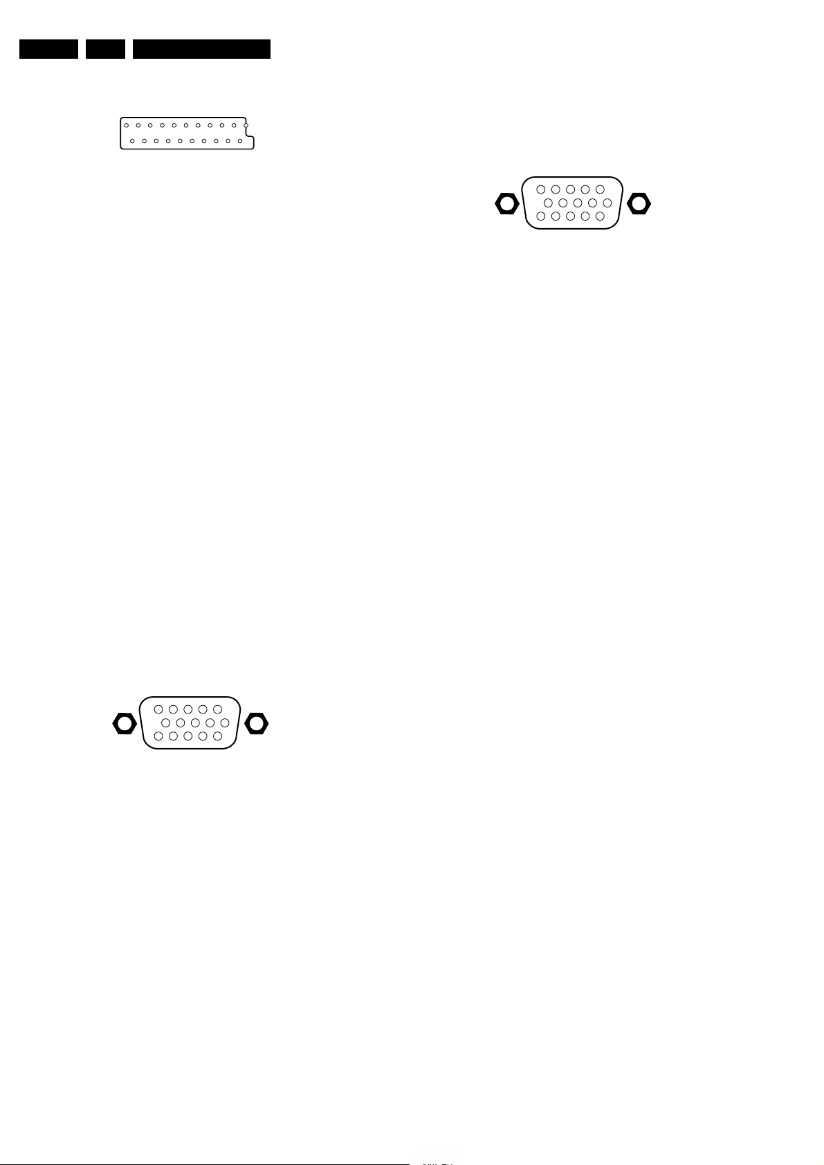
Monitor - Out (Sub-D: RGB+H/V, UART)
1
6
11
5
10
15
CL 16532023_043.eps
210901
Figure 1-7 VGA connector
1 - Red 0.7 V_pp/75 Ohm
2 - Green 0.7 V_pp/75 Ohm
3 - Blue 0.7 V_pp/75 Ohm
4 - Data 2 n.c.
5 - Test Ground
6 - Red Ground
7 - Green Ground
8 - Blue Ground
9-RC
10 - Ground
11 - Data 0 CONFIG_IDENT
12 - Data 1 UART - TXD
13 - H-sync
14 - V-sync
15 - Data 3 UART - RXD
EXT5: SD - In (YPbPr, Audio)
- - Y 1 V_pp/75 Ohm
- - Pr 0.7 V_pp/75 Ohm
- - Pb 0.7 V_pp/75 Ohm
- - Audio - L 0.5 V_rms/1 kOhm
- - Audio - R 0.5 V_rms/1 kOhm
PC/MAC - In (Sub-D: RGB+H/V)
1
6
11
5
10
15
CL 16532023_043.eps
210901
Figure 1-6 VGA connector
1 - Red 0.7 V_pp/75 Ohm
2 - Green 0.7 V_pp/75 Ohm
3 - Blue 0.7 V_pp/75 Ohm
4 - Data 2 n.c.
5 - Test Ground
6 - Red Ground
7 - Green Ground
8 - Blue Ground
9-n.c.
10 - Ground
11 - Data 0 n.c.
12 - Data 1 n.c.
13 - H-sync 0 - 5 V/1 kOhm
14 - V-sync 0 - 5 V/1 kOhm
15 - Data 3 n.c.
Audio PC/MAC - In (Cinch: VGA1, Centre)
1 - Centre 0.5 V_rms/10 kOhm
2 - Audio L 0.5 V_rms/10 kOhm
3 - Audio R 0.5 V_rms/10 kOhm
Page 5
Technical Specifications, Connections, and Chassis Overview
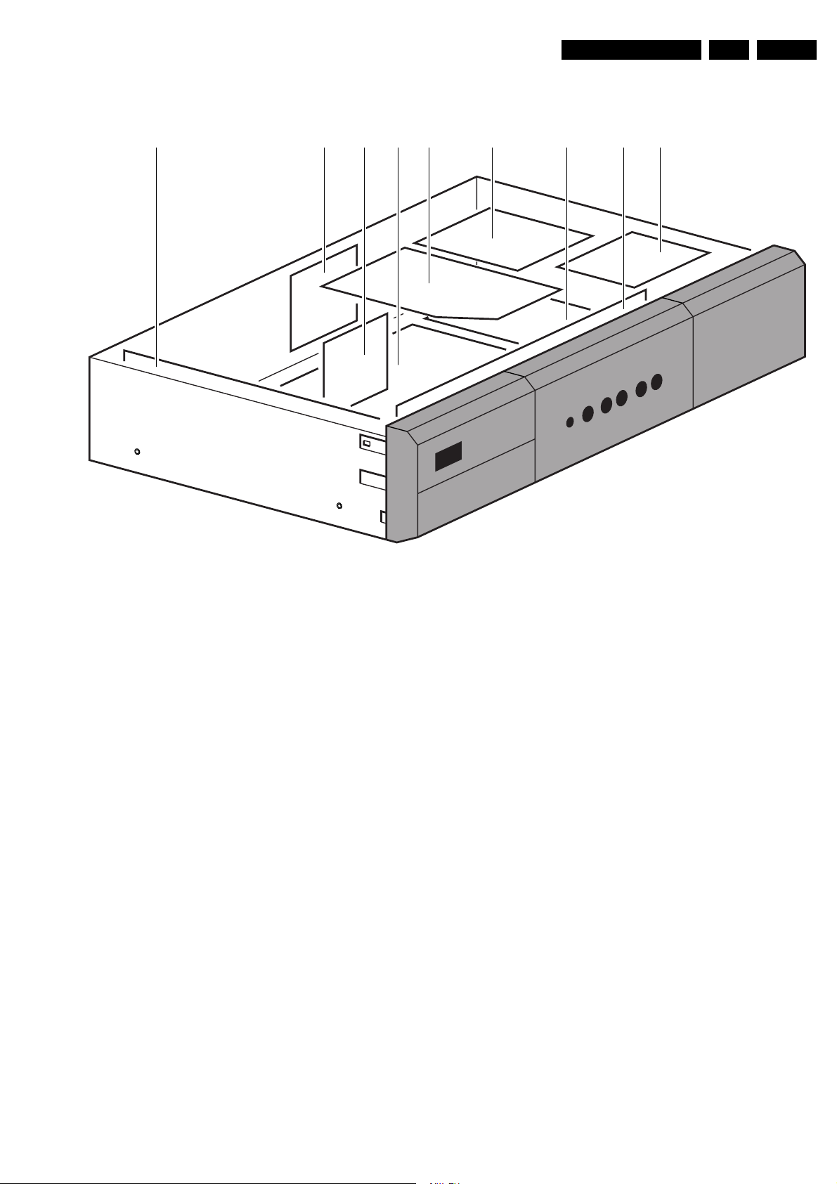
1.3 Chassis Overview
2 68 7 4 3 95 1
EN 5F21RE AB 1.
1. Front I/O Panel (FP).
2. Power Supply Panel (PS).
3. Double Window Panel (if present).
4. Feature Box (FBX).
5. Small Signal Panel (SSP).
6. Audio Video Interface Panel (AVI).
7. Scaler Panel (if present).
8. Standard Definition Connector Panel (SD).
9. 3D Comb Panel (C)
CL 26532054_008.eps
150502
Figure 1-8 Panel position
Page 6

EN 6 F21RE AB2.
Safety Instructions, Warnings, and Notes
2. Safety Instructions, Warnings, and Notes
2.1 Safety Instructions
Safety regulations require that during a repair:
• Connect the Receiver box to the mains via an isolation
transformer.
• When you use the Receiver box in combination with a
plasma monitor, do not operate the monitor without the
front glass plate. One function of this glass plate is to
absorb IR radiation. Without this glass plate, the level of
radiation could damage your eyes.
• Safety components, indicated by the symbol , must be
replaced with original components.
Safety regulations require that after a repair, you must return
the set in its original condition. Pay particular attention to the
following points:
• Route the wire trees in their original positions and fix them
in place with the mounted cable clamps.
• Check the insulation of the mains lead for external
damage.
• Check the electrical DC resistance between the mains plug
and the secondary side (only for sets which have an mains
isolated power supply):
– Unplug the mains cord and connect a wire between the
two pins of the mains plug;
– Set the mains switch to the "on" position (keep the
mains cord unplugged!).
– Measure the resistance value between the pins of the
mains plug and the metal shielding of the tuner or the
aerial connection on the set. The reading should be
between 4.5 MOhm and 12 MOhm.
– Set the mains switch to the "off" position, and remove
the wire between the two pins of the mains plug.
• Check the cabinet for defects, to prevent the customer from
touching any inner parts of the television set.
2.2 Warnings
• All ICs and many other semiconductors are susceptible to
electrostatic discharges (ESD symbol ). Careless
handling during repair can reduce life drastically. Make
sure that, during repair, you are connected with the same
electrical potential as the set by a wristband with
resistance. Keep components and tools at this same
potential. Available ESD protection equipment:
– Complete ESD3 kit (small tablemat, wristband,
connection box, extension cable and earth cable):
4822 310 10671.
– Wristband tester: 4822 344 13999.
• Be careful while taking measurements in the live voltage
section.
• Never replace modules, or other components, with the
television set "'ON."
• Use plastic tools, instead of metal tools, when performing
alignments on the television set. This will help prevent
short circuits and reduce the danger of a circuit becoming
unstable.
stereo sound (L: 3 kHz, R: 1 kHz unless stated otherwise)
and picture carrier at 61.25 MHz (NTSC).
• Where necessary, measure the oscillograms and direct
voltages with (symbol ) and without (symbol ) aerial
signal. Measure the voltages in the power supply section
both in normal operation (symbol ) and in standby
(symbol ). These values are indicated by means of the
appropriate symbols.
• The semiconductors indicated in the circuit diagram and in
the parts lists, are interchangeable position with the
semiconductors in the unit, irrespective of the type
indication on these semiconductors.
2.3.2 Schematic Notes
• All resistor values are in ohms and the value multiplier is
often used to indicate the decimal point location (e.g. 2K2
indicates 2.2 kOhm).
• Resistor values with no multiplier may be indicated with
either an 'E' or an 'R' (e.g. 220E or 220R indicates 220
Ohm).
• All Capacitor values are expressed in Micro-Farads (µ =
-6
x10
), Nano-Farads (n = x10-9), or Pico-Farads (p = x10
12
).
• Capacitor values may also use the value multiplier as the
decimal point indication (e.g. 2p2 indicates 2.2 pF).
• An 'asterisk' (*) indicates component usage varies. Refer to
the diversity tables for the correct values.
• The correct component values are listed in the Electrical
Replacement Parts List. Therefore, always check this list
when there is any doubt.
2.3.3 Practical Service Precautions
• It makes sense to avoid exposure to electrical shock.
While some sources are expected to have a possible
dangerous impact, others of quite high potential are of
limited current and are sometimes held in less regard.
• Always respect voltages. While some may not be
dangerous in themselves, they can cause unexpected
reactions - reactions that are best avoided. Before reaching
into a powered TV set, it is best to test the high voltage
insulation. It is easy to do, and is a good service precaution.
• Before powering up the TV set with the rear cover off
(or on a test fixture), attach a clip lead to the CRT DAG
ground and to a screwdriver blade that has a well insulated
handle. After the TV is powered on and high voltage has
developed, probe the anode lead with the blade, starting at
the case of the High Voltage Transformer (flyback - IFT).
Move the blade to within two inches of the connector of the
CRT.
If there is an arc, you found it the easy way, without
getting a shock!
If there is an arc to the screwdriver blade, replace the part
that is causing the problem: the High Voltage Transformer
or the lead (if it is removable).
-
2.3 Notes
2.3.1 General
• Measure the direct voltages and oscillograms with regard
to the chassis ground (symbol ), or hot ground
(symbol ).
• The direct voltages and oscillograms shown in the
diagrams are indicative. Measure them in the Service
Default Mode (see chapter 5) with a colour bar signal and
Page 7
3. Directions for Use
Directions for Use
EN 7F21RE AB 3.
Page 8
EN 8 F21RE AB3.
Directions for Use
Page 9
Directions for Use
EN 9F21RE AB 3.
Page 10
EN 10 F21RE AB3.
Directions for Use
Page 11
Directions for Use
EN 11F21RE AB 3.
Page 12
EN 12 F21RE AB3.
Directions for Use
Page 13
Directions for Use
EN 13F21RE AB 3.
Page 14
EN 14 F21RE AB3.
Directions for Use
Page 15
Directions for Use
EN 15F21RE AB 3.
Page 16
EN 16 F21RE AB3.
Directions for Use
Page 17
Directions for Use
EN 17F21RE AB 3.
Page 18
EN 18 F21RE AB3.
Directions for Use
Page 19
Directions for Use
EN 19F21RE AB 3.
Page 20
EN 20 F21RE AB3.
Directions for Use
Page 21
Directions for Use
EN 21F21RE AB 3.
Page 22
EN 22 F21RE AB3.
Directions for Use
Page 23
Directions for Use
EN 23F21RE AB 3.
Page 24
EN 24 F21RE AB3.
Directions for Use
Page 25
Directions for Use
EN 25F21RE AB 3.
Personal Notes:
Page 26
EN 26 F21RE AB4.
3
Mechanical instructions
4. Mechanical instructions
Index of this chapter:
1. Disassembly and Panel Overview
1. Top Cover Removal
2. Panel Overview
2. Service Positions and Panel Removal
1. Front I/O Panel
2. Double Window Panel (if present)
3. Power Supply Panel
4. Feature Box Module
5. Small Signal Panel
6. Down Scaler Panel (if present)
7. Audio/Video Interface Panel
8. High Definition Panel
9. 3D Comb Panel (US only)
3. Re-assembly
Note: Figures below can deviate slightly from the actual
situation, due to the different set executions.
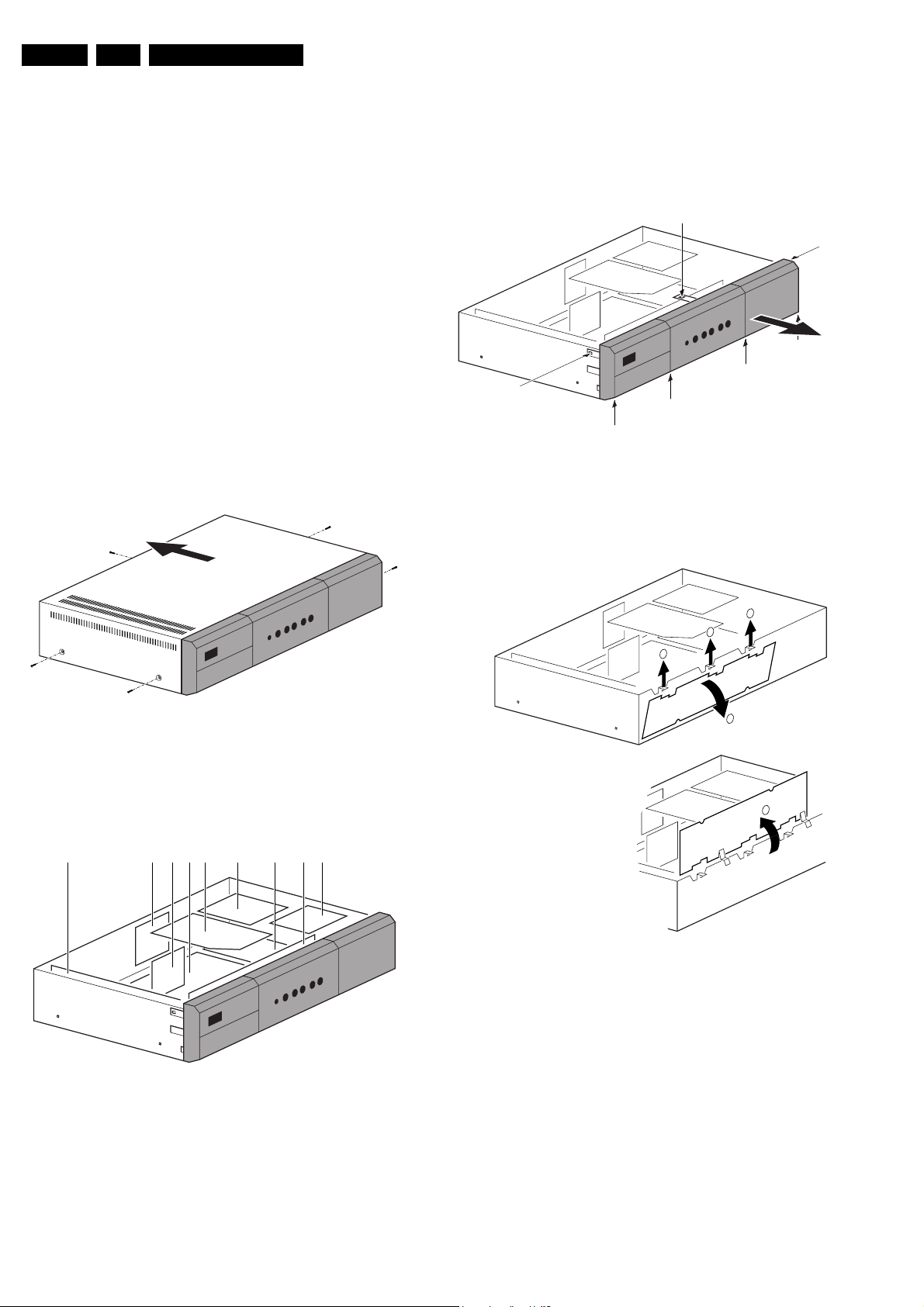
4.1 Disassembly and Panel Overview
4.1.1 Top Cover Removal
4.2 Service Positions and Panel Removal
4.2.1 Front I/O Panel
A
A
A
A
A
Figure 4-3 Front cover removal
Remove the front cover plate:
1. Pull the lugs [A] on top, bottom, and both sides of the
receiver box slightly aside.
2. Pull the front panel in the direction of the big arrow.
A
CL 26532054_009.eps
150502
A
Figure 4-1 Top cover removal
1. For safety reasons, first unplug the mains cable.
2. Remove all fixation screws of the metal top cover.
3. Remove the metal top cover.
4.1.2 Panel Overview
2 68 7 4 3 95 1
Figure 4-2 Panel overview
1. Front I/O.
2. Power Supply.
3. Double Window Panel (if present).
4. Feature Box.
5. Small Signal Panel.
6. Audio Video Interface.
7. Down Scaler panel (if present).
8. High Definition panel.
9. 3D Comb panel (US version only).
CL 16532098_012.eps
140901
CL 26532054_008.eps
150502
1
1
1
2
CL 16532098_015.eps
180901
Figure 4-4 Service position Front I/O panel
Remove the front I/O panel:
1. Lift the clamps [1] to release the Front I/O panel.
2. Unlock the Front I/O panel from the receiver box [2].
3. Park the front I/O panel on top of the housing [3]. Use a
protection sheet to prevent short-circuiting.
Note: Be sure to keep track of the three copper grounding clips;
they can be lost very easily, or they can cause short circuiting
when falling into the receiver box.
Page 27
Mechanical instructions
EN 27F21RE AB 4.
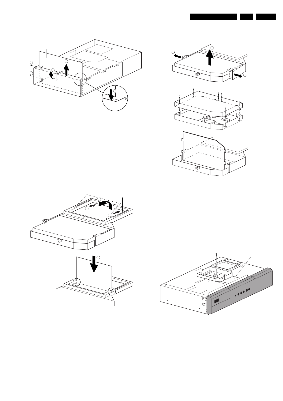
4.2.2 Power Supply Panel
PS panel
1
1
3
2
Figure 4-5 Service position Power Supply (PS)
1. Remove the front panel, if it was not yet removed.
2. Remove the screws [1].
3. Remove the fixation bracket [2].
4. Pull the Power Supply panel out of the receiver box [3].
5. Place the Power Supply panel in the small slots on the
edges of the top of the housing [4].
4
CL 16532098_016.eps
240901
4.2.4 Feature Box module
FBX Module
2
1
1
Warning: Be aware of the live voltages on this board
during operation!
4.2.3 Double Window Panel (if present)
1
Figure 4-6 Service position Double Window panel
CL 16532098_014.eps
140901
Figure 4-7 Service position Feature Box panel (FBX)
2
DW panel
1. Pull the clamps aside [1], and lift the Feature box module
[2].
2. Disconnect the cables and take out the module.
1
DW/FBX bracket
3. Remove the shielding of the module: de-solder the fixation
lugs.
4. Remove the Feature Box panel from the module.
5. Connect the cables and place the Feature Box panel in
service position in the regarding bracket.
4.2.5 Small Signal Panel
3
CL 26532054_010.eps
150502
SSP panel
CL 16532098_031.eps
140901
When the metal top cover is removed, the Double Window
panel is accessible.
For the service position:
1. Release the clamps [1] and push the panel gently up and
out of its bracket [2].
2. One of the cables must be temporarily disconnected to
place the Double Window panel in its service position as
shown in the figure.
3. Lead the removed cable in a favourable position and
connect this cable again.
Figure 4-8 Removal of the Feature Box bracket
1. Release the clamps that secure the feature box module.
2. Lift the feature box module, disconnect the regarding
cables and take out the module.
3. Release the side clamps that secure the Feature box
bracket.
4. Remove the screw in the middle of the feature box position
and remove the complete bracket.
Page 28
EN 28 F21RE AB4.
E
D
E
D
C
C
F
G
D
C
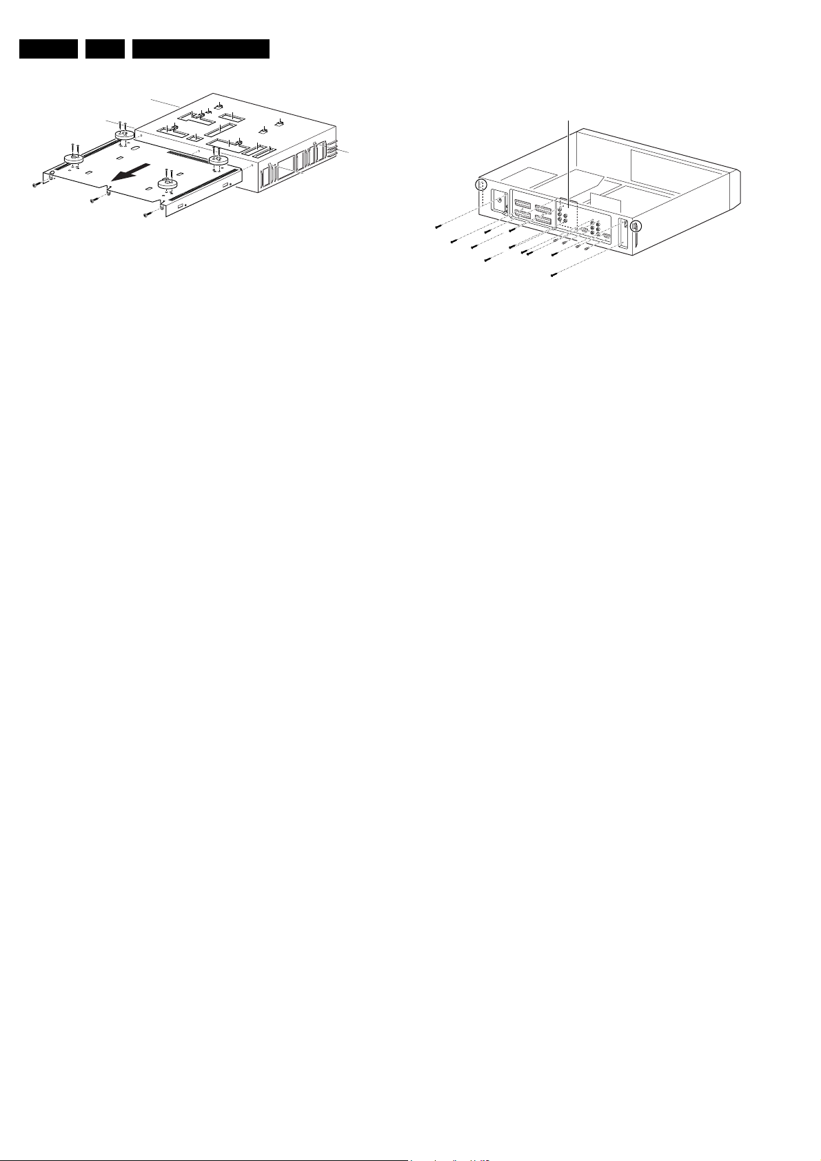
Figure 4-9 Removal of the bottom cover plate
To access the copper side of the Small Signal Panel, it is
necessary to remove the metal bottom cover:
1. Turn the TV receiver box upside down.
2. Remove the three screws [C] that secure the bottom plate
at rear side.
3. Remove the screws [D] that hold the four feet and remove
the feet.
4. Pull the metal bottom cover backwards (lift it over the studs
[E]). Be aware of the hooks [F] on the frame.
Remove the Small Signal Panel:
1. Disconnect all cables.
2. Remove at rear side of the receiver box the three mounting
screws that secure this panel to the back plate.
3. Release the clamps that secure the Small Signal Panel and
carefully take it out.
4.2.6 Audio Video Interface panel
If the metal bottom cover is removed, the copper side of the AVI
panel is accessible.
Remove the Audio Video Interface panel
1. Make sure that the Feature Box module and its bracket is
removed as described above.
2. Disconnect all cables.
3. Remove at rear side of the TV receiver box the three
mounting screws that secure this panel to the backside.
4. Remove the four distance stud screws belonging to the PC/
MAC IN and MONITOR OUT sockets.
5. Release the clamps that secure the Audio video interface
and carefully take out the Small Signal Panel.
4.2.7 Down Scaler Panel (if present)
1. This Down Scaler panel stands normally in an upright
service position.
2. To remove this panel: pull it firmly out of its connectors,
mounted on the Audio Video Interface.
F
F
F
G
G
G
G
D
F
F
H
H
H
Mechanical instructions
4.2.8 HD/SD (High/Standard Definition) Panel
F
E
E
CL 16532098_025.eps
180901
4.2.9 3D Comb panel (US only)
4.3 Reassembly
HD/SD panel
J
G
G
K
G
K
G
G
H
H
H
G
G
H
G
G
J
CL 36532021_013.eps
Figure 4-10 Removal of the HD/SD connector panel
There is no service position defined for this panel. The best way
to perform measurements on this panel is to remove the
Feature Box bracket as described above. Then the component
side of this single sided panel is accessible.
To remove the HD/SD panel:
Unscrew the screws that hold the panel (on the inside of the TV
receiver).
1. Remove both mounting screws
2. Turn it in a favourable position and lift it (if necessary
release and lift the Feature Box bracket a fraction at right
side).
3. Release the cable from the special shaped cable clamp.
Note: Use a protection sheet to prevent short-circuiting if you
place the unit in service position.
1. If necessary, you can remove the panel from its bracket. To
do this, release the clamps that secure the panel in the
bracket and remove the panel out of the bracket.
• To re-assemble the TV receiver, perform the disassembly
processes in reversed order.
• Before re-placing the top cover, verify the correct
connections for all the cables, and lead the cables in the
original positions.
270303
Note: Be sure to keep track of the two copper grounding clips;
they can be lost very easily, or they can cause short circuiting
when falling into the receiver box.
Page 29

Service Modes, Error Codes, and Fault Finding
5. Service Modes, Error Codes, and Fault Finding
EN 29F21RE AB 5.
Index of this section:
1. Test Points
2. Service Modes
3. Problems and Problem Solving Tips (related to CSM).
4. ComPair
5. Error Codes
6. Protections
7. Repair Tips
5.1 Test Points
5.1.1 General
Perform measurements under the following conditions:
• Set in Service Default Mode.
• Video: Colour bar signal, received via the internal tuner.
• Audio: 3 kHz left, 1 kHz right.
Exceptions (when using external sources):
• Set in Service Default Mode (SDM).
• Video: If using a DVD player, use a "live" picture. If using a
VGA source, use a picture of your choosing.
• Audio: You can use a service generator, or the audio from
the DVD player or VGA source.
5.1.2 Waveforms
The chassis is equipped with test points printed on the circuit
board assemblies. Test points are displayed in two different
ways:
• The old method, still in use for re-used circuits (like the
Small Signal Panel, the Double Window Panel, and the
Feature Box), refers to the functional blocks. The test
points have names starting with I for IF, S for sound, etc.
The numbering is in a logical sequence for diagnostics.
• The new method, used for new circuits, uses service test
points that are recognizable as tagged Fxxx points. With
this method, factory test points are published (F-points are
functional test points, I-points are test points for in-circuit
testers in the factory. All these test points are on the copper
side. When the test point is a service test point, it is tagged
for recognition.
Not all test points have been measured, but they can serve as
identification names in Service communication (for example,
ComPair fault find trees, Searchman files).
In the following cases, there will also be no waveform:
• When a Vdc voltage is displayed in the diagrams, or when
the waveform does not have an additional value.
• When the sources are not easy accessible for the Service
engineer (for example, VGA source).
• External AV inputs are not measured, since the waveform
is equal to the source (dependent of load resistor
matching).
5.1.3 DC voltages
The DC voltages are measured at practically all semiconductor
pins. These values are displayed in the circuit diagrams. If a DC
value is displayed between brackets then this value is
measured in "standby" mode.
Note: DC voltages are also measured on the connectors.
5.2 Service Modes
There is also the option of using ComPair, a hardware interface
between a computer (see requirements) and the FTV chassis.
It offers the ability of structured troubleshooting, a test pattern
generation, error code reading, software version readout, and
software upgrading. (Software upgrading is not available for all
chassis)
Minimum requirements for ComPair: a Pentium Processor,
Windows 9x/NT/2000/XP/ME, and a CD-ROM drive (see
"ComPair" section).
5.2.1 Service Default Mode (SDM)
Purpose
• To create a pre-defined setting to get the same
measurement results as given in this manual.
• To override SW protections (only when SDM is entered via
the “service pins” on SSP connector 0356).
• To start the "blinking LED" procedure.
Specifications
• Tuning frequency: 475.25 MHz for PAL/SECAM (the
source is displayed on the screen)
• Colour system: SECAM L for France and PAL B/G for the
rest of Europe.
• All picture settings at 50 % (brightness, colour, contrast).
• Bass, treble and balance at 50 %; volume at 25 %.
• All service-unfriendly modes (if present) are disabled. The
service unfriendly modes include:
– Sleep timer.
– Smart modes.
– On Timer.
– Child lock.
– Black mute.
How to enter SDM
To enter SDM, use one of the following methods:
• Press the following key sequence on the remote control
transmitter: 062596 directly followed by MENU.
• Short pins 2 and 3 on connector 0356 of the SSP (the two
pins that are nearest to the rear panel) while the set is in
the normal operation mode.
Caution: Entering SDM by this method will override all
processor-controlled protections. When doing this, the service
technician must know exactly what he is doing, as this could
damage the set.
• Use the Dealer Service Tool (DST) emulation feature of
ComPair.
After entering SDM, a blank screen is visible, with "Service
Default" in the upper part for recognition. The “blinking LED”
procedure is started and will indicate any possible errors via the
front LED.
How to navigate in SDM
To toggle to the SAM mode, press the following key sequence
on the remote control transmitter: 062596 directly followed by
OSD (i+).
How to exit SDM
Switch the set to STANDBY by pressing the POWER button on
the remote control transmitter (if you switch the set OFF by
disconnecting the mains cable, the set will remain in SDM
when mains is reapplied).
Service Default Mode (SDM) and Service Alignment Mode
(SAM) offer several features for the service technician, while
the Customer Service Mode (CSM) is used for communication
between the servicer and the customer.
Page 30
EN 30 F21RE AB5.
Service Modes, Error Codes, and Fault Finding
5.2.2 Service Alignment Mode (SAM)
Purpose
• To perform (software) alignments.
• To change the option settings.
• Easy identification of the software version.
• To view operational hours.
• To display (or clear) the error code buffer.
• To give the service technician the possibility (through a
special sequence of navigating and selecting) to diagnose
F21R problems with a standard PC monitor.
Specifications
• Software version of main processor.
• Operational hours counter.
• Dealer options.
• Service options.
• Error buffer reading and erasing.
• Alignments.
• Functional test.
How to enter SAM
Use one of the following methods:
• Press the following key sequence on the remote control
transmitter: 062596 directly followed by OSD (i+).
• Short jumpers 1 and 2 of connector 0356 on the SSP (the
two pins that are nearest to the front panel).
• Use the "Align" key of the Dealer Service Tool (DST)
emulation feature of ComPair.
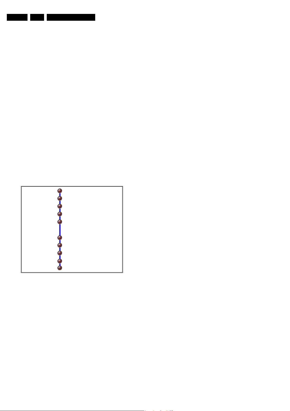
After entering SAM, the following screen is visible:
Rom Version
Operating Hours
Errors
Defective Module
Reset Error Buffer
Alignments
Dealer Options
Service Options
Store Options
Functional Test
Aug 24 2001 F21RE1_1.0_xxxxx
No Errors
None
Figure 5-1 SAM screen shot
• OPERATION HOURS. The accumulated total of operation
hours of the Receiver box. Every time the Receiver box is
switched "on", 0.5 hour is added to the operation hours
counter.
• HARDWARE INFO. Indicates the software date and
version (MMMDDYYYY AAAABC_X.Y_xxxxx) of the box.
– MMMDDYYY = software date
– AAAA = the chassis name.
– B = the region (E= Europe, A= Asia Pacific, U= NAFTA,
L= LATAM or G= Global).
– C = the language cluster (1= English).
– X = the main software version number.
– Y = the sub software version number.
– xxxxx = the last five digits of the 12nc code.
• ERRORS. Room for a maximum of 10 errors. The most
recent error is displayed at the upper left position. For an
explanation of the errors, see the error code table in the
"Error Codes" section.
• DEFECTIVE MODULE. The module that generates an
error is displayed here. If there are multiple errors in the
CL 16532023_044.eps
210901
buffer that have not all been generated by a single module,
there is probably another defect. In that situation, the
message "Unknown" will then be displayed here. If there
are no errors, "None" is displayed.
• RESET ERROR BUFFER. Erases the contents of the error
buffer. Press "OK" on the remote control transmitter to do
this; the error buffer is cleared.
• ALIGNMENTS. Navigation by sub menus to service
alignment items. The details of these alignments are
explained in the "Electrical Alignments" section.
• DEALER OPTIONS. Controls the demonstration modes
used by dealers for display purposes.
• SERVICE OPTIONS. In this sub menu, the options can be
set. The quickest method to do this is through HW option
number entry.
• STORE OPTIONS. Service options must be stored here.
Note: Without storing, no changes made to the options will
be recorded. The servicer must remember to store all
changes before exiting SAM for those changes to take
effect.
• FUNCTIONAL TEST. Activate this test by pressing the
"OK" key on the remote control transmitter. Eventual errors
are displayed in the error buffer. The error buffer is not
erased, although it looks that way. By exiting SAM and then
entering SAM again, you will see the error buffer still
contains the previous contents.
How to navigate in SAM
Use one of the following methods:
• In SAM, select menu items with the "Cursor Up/Down"
keys on the remote control transmitter. The selected “ball”
item is highlighted and becomes a “puck” (blue becomes
yellow). When not all menu items fit on the screen, this is
shown by two "ball" figures overlapping. Use the " Cursor
Up/Down " keys to display the next / previous menu
item(s).
• With the "Cursor Left/Right" keys, it is possible to:
– (De)activate the selected menu item.
– Change the parameter of the selected menu item
(some times through a "slider" entry)
– Activate the selected submenu.
• To toggle to the SDM mode, press the following key
sequence on the remote control transmitter: 062596
directly followed by MENU.
Note: SAM is exited when the MENU button on the remote
control transmitter is pressed once. If SAM is exited
accidentally, you have to enter the SAM mode again to perform
SAM alignments and adjustments.
How to exit SAM
To exit SAM, press the MENU button on the remote control
transmitter once.
5.2.3 Customer Service Mode (CSM)
Purpose
The Customer Service Mode shows error codes and
information on the Flat TV operation settings. The servicer can
instruct the customer to enter CSM by telephone and read off
the information displayed. This helps the servicer to diagnose
problems and failures in the Flat TV set before making a
service call.
The CSM is a read-only mode; therefore, modifications are not
possible in this mode.
How to enter CSM
To enter CSM, use one of the following methods:
• Press the MUTE button on the remote control transmitter
and the MENU button on the local keyboard
simultaneously for at least four seconds.
• An alternative CSM entry method is to press the following
key sequence on the remote control transmitter: 123654.
Page 31

Service Modes, Error Codes, and Fault Finding
EN 31F21RE AB 5.
Do not allow the display to time out between entries while
keying the sequence. The disadvantage of this method is
that the selected source is changed, due to the key
sequence. Therefore, the first method is preferred.
Upon entering the Customer Service Mode, the following
screen will appear:
Customer Service Menu 1
• SET TYPE. This allows the customer to view the
(commercial) type number of the Receiver box, without
looking at the bottom of this box. This information can be
very helpful when talking with the service technician.
• AG NBR. First some explanation for understanding. On the
type plate of the E-box (bottom), you can see a PROD. NO:
AG-code (e.g. AG000312 xxxxxx): AG00 is a production
code, 0312 means production year 2003, week 12 and
xxxxxx is the series number of the set. On this screen line,
you can read the AG-code of the Receiver box, without
looking at the bottom of the E-box. This information can be
very helpful when talking with a dealer or Philips Customer
Care Centre (P3C). Currently this line is not filled in. At the
moment, you will see: **0000.... It will be implemented in
the future.
• SW VERSION. Indicates the software version
(AAAABC_X.Y_xxxxx) of the box.
– AAAA = the chassis name.
– B = the region (E= Europe, A= Asia Pacific, U= NAFTA,
L= LATAM or G= Global).
– C = the language cluster (1= English).
– X = the main software version number.
– Y = the sub software version number.
– xxxxx = the last five digits of the 12nc code.
• FEATUREBOX. Gives the 12nc of the used Feature Box
software.
• CODE 1. Gives the last five errors of the error buffer. As
soon as the built-in diagnosis software has detected an
error, the buffer is adapted. If there are no errors, the text
"0" is displayed.
• CODE 2. Gives the first five errors of the error buffer. As
soon as the built-in diagnosis software has detected an
error, the buffer is adapted. The most recent error is
displayed on the leftmost position of the Code 2 line. Each
error code is displayed as a 3-digit number. When less than
10 errors occur, the rest of the line(s) is (are) empty. If there
are no errors, the text "0" is displayed. See the "Error
Codes" section for a description of the error codes. Service
Tip: When a group of adjacent errors has a specific colour,
this means they have occurred in the same time window.
This gives service technicians additional information.
• VOLUME. Shows the last status of the volume, as set by
the customer. The parameter can vary from 0 (minimum) to
100 (maximum). Volume parameters can be changed by
using the volume key on the remote control transmitter.
Note: For "speaker less" TV monitors, this item is not
shown.
• BRIGHTNESS. Gives the last status of the brightness, as
set by the customer. The parameter can vary from 0
(minimum) to 100 (maximum). The brightness parameter
can be changed by using the CURSOR LEFT and
CURSOR RIGHT keys on the remote control transmitter
after pressing the "menu" button and navigating to "picture"
and setting "brightness".
• CONTRAST. Gives the last status of the contrast, as set by
the customer. The parameter can vary from 0 (minimum) to
100 (maximum). Contrast parameters can be changed by
using the CURSOR LEFT and CURSOR RIGHT keys on
the remote control transmitter after pressing the "menu"
button and navigating to "picture" and setting "contrast".
• COLOUR. Gives the last status of the colour saturation, as
set by the customer. The parameter can vary from 0
(minimum) to 100 (maximum). Colour parameters can be
changed by using the CURSOR LEFT and CURSOR
RIGHT keys on the remote control transmitter after
pressing the "menu" button and navigating to "picture" and
setting "colour".
• HUE. Gives the last status of the colour saturation, as set
by the customer. The parameter can vary from -50
(minimum) to 50 (maximum). Hue parameters can be
changed by using the CURSOR LEFT and CURSOR
RIGHT keys on the remote control transmitter after
pressing the "menu" button and navigating to "picture" and
setting "hue".
You can select the next Customer Service Mode screen(s) by
pressing the CURSOR DOWN key on the remote control
transmitter. To return to the previous Customer Service Mode
screen(s), press the CURSOR UP key on the remote control
transmitter (there are 4 CSM menu screens).
Customer Service Mode Screen 2
• SHARPNESS. Gives the sharpness parameter, as set by
the user. It can vary from 0 (minimum) to 7 (maximum). A
noisy picture may result if there is a bad antenna signal, or
the parameter of sharpness is set too high. Sharpness
parameters can be changed by using the CURSOR LEFT
and CURSOR RIGHT keys on the remote control
transmitter after pressing the "menu" button and navigating
to "picture" and setting "sharpness".
• HEADPHONE VOLUME. Gives the last status of the
headphone volume, as set by the customer. The parameter
can vary from 0 (minimum) to 100 (maximum). Headphone
volume parameters can be changed by using the CURSOR
LEFT and CURSOR RIGHT keys on the remote control
transmitter after pressing the "menu" button and navigating
to "sound" and setting "headphone volume".
• CENTRE MODE. Indicates the loudspeaker configuration
of the monitor. If it is set to "On", then the internal speakers
both produce centre sound (from the "centre input" input
jack on the back of the set). If it is set to "Off", the speakers
produce left and right sound. This parameter can be
changed by using the CURSOR LEFT and CURSOR
RIGHT keys on the remote control transmitter after
pressing the "menu" button and navigating to "Settings",
"General" and choosing "Centre mode" = “On". Note: For
"speaker less" TV monitors, this item is not shown.
• SOUND MODE. Indicates the selected sound mode, as
selected by the customer. This can be "Stereo", or "Mono".
This parameter can be changed by using the CURSOR
LEFT and CURSOR RIGHT keys on the remote control
transmitter after pressing the "menu" button and navigating
to "Settings", "General" and choosing "Sound mode".
• TUNER FREQUENCY. Gives the frequency of the main
Tuner in MHz.
• INCREDIBLE SURROUND. Indicates the by the customer
selected surround mode. This can be 'On' or 'Off'. Note:
For "speaker less" TV monitors, this item is not shown.
• DIGITAL NATURAL. Indicates the, by the customer
selected, Digital Natural Motion mode. This can be 'On' or
'Off'. This parameter can be changed via the 'cursor left'
and 'cursor right' keys on the remote control handset after
pressing the 'menu'-key and navigating to 'Menu', 'Picture'
and choosing 'Dig natural motion'.
• TV SYSTEM. Gives information about the video system of
the selected transmitter.
– BG: PAL BG signal received
– DK: PAL DK signal received
– I: PAL I signal received
– L/La: SECAM L/L' signals received
– M38.9: NTSC M signal received with video carrier on
38.9 MHz
– MN: NTSC M signal received
Customer Service Mode Screen 3
• BALANCE. Gives the last status of the balance, as set by
the customer. The parameter can vary from -50 (maximum
left balance) to 50 (maximum right balance). Balance
parameters can be changed by using the CURSOR LEFT
Page 32

EN 32 F21RE AB5.
Service Modes, Error Codes, and Fault Finding
and CURSOR RIGHT keys on the remote control
transmitter after pressing the "menu" button and navigating
to "sound" and setting "balance".
• DNR. This is the setting of Dynamic Noise Reduction. This
can be set to "Off", "minimum", "medium", or "maximum".
• NOISE FIGURE. Gives the selected noise ratio for the
selected transmitter. This parameter can vary from 0 (good
signal) to 255 (bad signal).
Note: This measured value only has significance when the
"active control" mode is activated (this can be done by pressing
the "active control" key on your remote control transmitter).
• SOURCE. This source parameter can be changed by using
the CURSOR LEFT and CURSOR RIGHT keys on the
remote control transmitter after pressing the "menu" button
and navigating to "Menu", "Setup", and choosing "Source".
The "quality" parameter depends how you connect your
source: for example, if you connected the source to the
Video input or to the SVHS input. This can be set to
– Tuner (default)
– EXT1.
– EXT2.
– EXT3.
– EXT4.
– EXT5.
– Front.
– VGA. Behind this source value there is an item
referring to the "quality" of the chosen source:
– Tuner (default)
– VIDEO/STEREO.
– VIDEO/NICAM.
– S-VIDEO/STEREO.
– S-VIDEO/NICAM.
– RGB/STEREO.
– YUV/STEREO.
– YPBPR 1FH/STEREO.
• AUDIO SYSTEM. Gives information about the audio
system of the selected transmitter.
– Analog Mono.
– Analog Stereo.
– PCM 2/0.
– DD: 1/0, 2/0 LtRt, 2/0 L0R0, 2/1, 2/2, 3/0, 3/1, 3/2, or
1+1.
– MPEG: 1/0, 2/0, 2/0 LtRt, 2/1, 2/2, 3/0, 3/1, 3/2, 1+1,
2+2.
• TUNED BIT. Gives information about the tuning method of
the stored preset.
– If a channel is detected by searching (manual as well
as automatic installation), the micro-search tuning
algorithm is used. When a channel is identified and
stored, this will display YES.
– When you install a preset (while the channel is not
being broadcast) with "digit entry"/"fine tune", the
display (after storing) will read NO. If the channel is
found later (after a successful micro-search), the tuned
bit will change to "Yes". If the tuned bit displays "No",
something is wrong with the installed preset. Please
reinstall the preset.
Customer Service Mode 4
• ON TIMER. Gives information about the timer settings.
This can be:
– Off.
– On.
– Time (e.g. 18.25).
– Day (e.g. Monday).
– Program Number (e.g. PR23).
• PRESET LOCK. Gives the status info. This can be:
– Unlock.
– Locked.
• CHILD LOCK. Gives the status info. This can be:
– Unlock.
– Locked.
– Custom.
• AGE LOCK. Gives the status info. This can be:
– Off.
– 4, 6, 8, 10, 12, 14, or 16 years.
• LOCK AFTER. Gives the status info. This can be:
– Off.
– Time (e.g. 18.45).
• CATEGORY LOCK. Gives the status info. This can be:
– Off
– Movies, News, Shows, Sports, Children, Music, or
Culture.
• PROGRAM CATEGORY. Gives the status info. This can
be:
– Off
– Movies, News, Shows, Sports, Children, Music, or
Culture.
• SW CODE 1. This code is only for Development. Do not
use it.
• SW CODE 2. This code is only for Development. Do not
use it.
5.3 Problems and Solving Tips (Related to CSM)
5.3.1 Picture Problems
Note: The problems described below are related to the TV
settings (customer settings). The procedures to change the
parameters (or status) of the different settings are described.
Snowy/noisy picture
Check the NOISE FIGURE line. If the value is 127 or higher
and is also high on other programs, check the aerial cable/
aerial system.
Picture too dark
• Press the "Smart Picture" button on the remote control
transmitter. If the picture improves, increase the brightness
value or increase the contrast value. The new value(s) are
automatically stored for all TV channels.
• If the picture improves after entering CSM, increase the
brightness value or increase the contrast value. The new
value(s) are automatically stored for all TV channels.
• Check the BRIGHTNESS and CONTRAST lines. If the
value of BRIGHTNESS is low (<15) or the value of
CONTRAST is low (<15), increase the brightness value or
increase the contrast value.
Picture too bright
• Press the "Smart Picture" button on the remote control
transmitter. If the picture improves, reduce the brightness
value or reduce the contrast value. The new value(s) are
automatically stored for all TV channels.
• If the picture improves after entering CSM, reduce the
brightness value or reduce the contrast value. The new
value(s) are automatically stored for all TV channels.
• Check BRIGHTNESS and CONTRAST. If the value of
BRIGHTNESS is high (>60) or the value of CONTRAST is
high (>75), reduce the brightness value or increase the
contrast value.
Fading picture
Digital scan effect. Check the DNR line. The status of DNR is a
value between 0 and 100. There is no practical way to explain
the significance of this value. If the picture is fading, adjustment
of the DNR level may help. The DNR level can be adjusted by
the following navigation route: "Menu" - "Picture" - "DNR".
There are four different selectable levels.
White line around picture elements and text
• Press the "Smart Picture" button on the remote control
transmitter. If the picture improves, reduce the sharpness
value. The new value(s) are automatically stored for all TV
channels.
Page 33

Service Modes, Error Codes, and Fault Finding
EN 33F21RE AB 5.
• If the picture improves after entering CSM, reduce the
sharpness value. The new value(s) are automatically
stored for all TV channels.
• Check the SHARPNESS line. If the value is too high,
reduce the sharpness value. The new value(s) are
automatically stored for all TV channels.
Black picture and/or unstable picture
Improper signal is being received. Check the NOISE FIGURE
line. If the value is higher then 127, the signal is suspect. Check
your cable or aerial signal.
Black and white picture
Check the COLOUR line. If this value is low (<30), increase the
"Colour" value. The new value(s) are automatically stored for
all TV channels.
Menu text not sharp enough
• Press the "Smart Picture" button on the remote control
transmitter. If the picture improves, reduce the contrast
value. The new value(s) are automatically stored for all TV
channels.
• If the picture improves after entering CSM, reduce the
contrast value. The new value(s) are automatically stored
for all TV channels.
• Check the CONTRAST line. If this value is high (>75),
reduce the contrast value.
5.3.2 Sound problems (only with 'speakered' FTV-monitor connected)
No sound from left and right speaker.
Possible solutions:
• Press the "Smart Sound" button on the remote control
transmitter. If the sound improves, raise the volume value.
The new value(s) are automatically stored for all TV
channels.
• If the volume is acceptable after entering CSM, increase
the volume. The new value(s) are automatically stored for
all TV channels.
• Check the VOLUME line. If the value is low, increase the
"Volume" value. The new value(s) are automatically stored
for all TV channels.
Sound too loud from left and right speaker.
• Press the "Smart Sound" button on the remote control
transmitter. If the sound improves, reduce the volume
value. The new value(s) are automatically stored for all TV
channels.
• If the volume is acceptable after entering CSM, decrease
the volume. The new value(s) are automatically stored for
all TV channels.
• Check the VOLUME line. If the value is high, reduce the
"Volume" value. The new value(s) are automatically stored
for all TV channels.
5.4 ComPair
5.4.1 Introduction
ComPair (Computer Aided Repair) is a service tool for Philips
Consumer Electronics products. ComPair is a further
development of the DST (special remote control transmitter for
service), which allows faster and more accurate diagnostics.
ComPair has three big advantages:
ComPair helps you to quickly get an understanding on how to
repair the chassis in a short time by guiding you systematically
through the repair procedures.
ComPair allows very detailed diagnostics (on I2C level) and is
therefore capable of accurately indicating problem areas. You
do not have to know anything about I2C commands yourself
because ComPair takes care of this.
ComPair speeds up the repair time since it can automatically
communicate with the chassis (when the microprocessor is
working) and all repair information is directly available. When
ComPair is installed together with the Force electronic manual
of the chassis being serviced, schematics and PWBs are only
a mouse click away.
5.4.2 Specifications
ComPair consists of a Windows based faultfinding program
and an interface box between PC and the product. The
ComPair interface box is connected to the PC via a serial or
RS232 cable.
With the F21R Receiver box, the ComPair interface box and
the Receiver box communicate via a bi-directional infrared link.
The ComPair faultfinding program is able to detect and
diagnose problems occurring in the product. ComPair can
gather diagnostic information in two ways:
• Automatic (by communication with the Receiver box):
ComPair can automatically read out the contents of the
entire error buffer. Diagnosis is done on I2C level. ComPair
can access the I2C bus of the Receiver box. ComPair can
send and receive I2C commands to the microprocessor of
the Receiver box. In this way, it is possible for ComPair to
communicate (read and write) to devices on the I2C
busses of the Receiver box.
• Manually (by asking questions to you): Automatic
diagnosis is only possible if the microprocessor of the
Receiver box is working correctly, and only to a certain
extent. When this is not the case, ComPair will guide you
through the faultfinding tree by asking you questions (for
example, Does the screen give a picture? Click on the
correct answer: YES / NO), and showing you examples (for
example, Measure test point I7 and click on the oscillogram
you see on the oscilloscope). The servicer can answer by
clicking on a link (for example, text or a waveform picture)
that will bring you to the next step in the faultfinding
process.
By a combination of automatic diagnostics and an interactive
question and answer procedure, ComPair will enable you to
find most problems in a fast and effective way.
Beside fault finding, ComPair provides some additional
features like:
• Uploading or downloading of presets.
• Management of preset lists.
• Emulation of the Dealer Service Tool (DST).
• If both ComPair and the Force electronic service manual
are installed, all the schematics and the PWBs of the
product are available by clicking on the appropriate
hyperlink.
Example: Measure the DC-voltage on capacitor C2568
(Schematic/Panel) at the SSP.
– Click on the "Panel" hyperlink to automatically show
the PWB with a highlighted capacitor C2568.
– Click on the "Schematic" hyperlink to automatically
show the electronic position of the highlighted
capacitor.
5.4.3 How to Connect ComPair
1. First, install the ComPair Browser software on your PC
(read the installation instructions carefully).
2. Connect the RS232 interface cable between a free serial
(COM) port of your PC and the PC connector (marked
"PC") of the ComPair interface.
3. Connect the mains adapter to the supply connector
(marked "POWER 9V DC") on the ComPair interface.
4. Switch the ComPair interface OFF.
5. Switch the Receiver box OFF (and remove the mains).
6. Point the ComPair interface to the Service send-LED
(behind the cover) on the front of the Receiver box.
Page 34
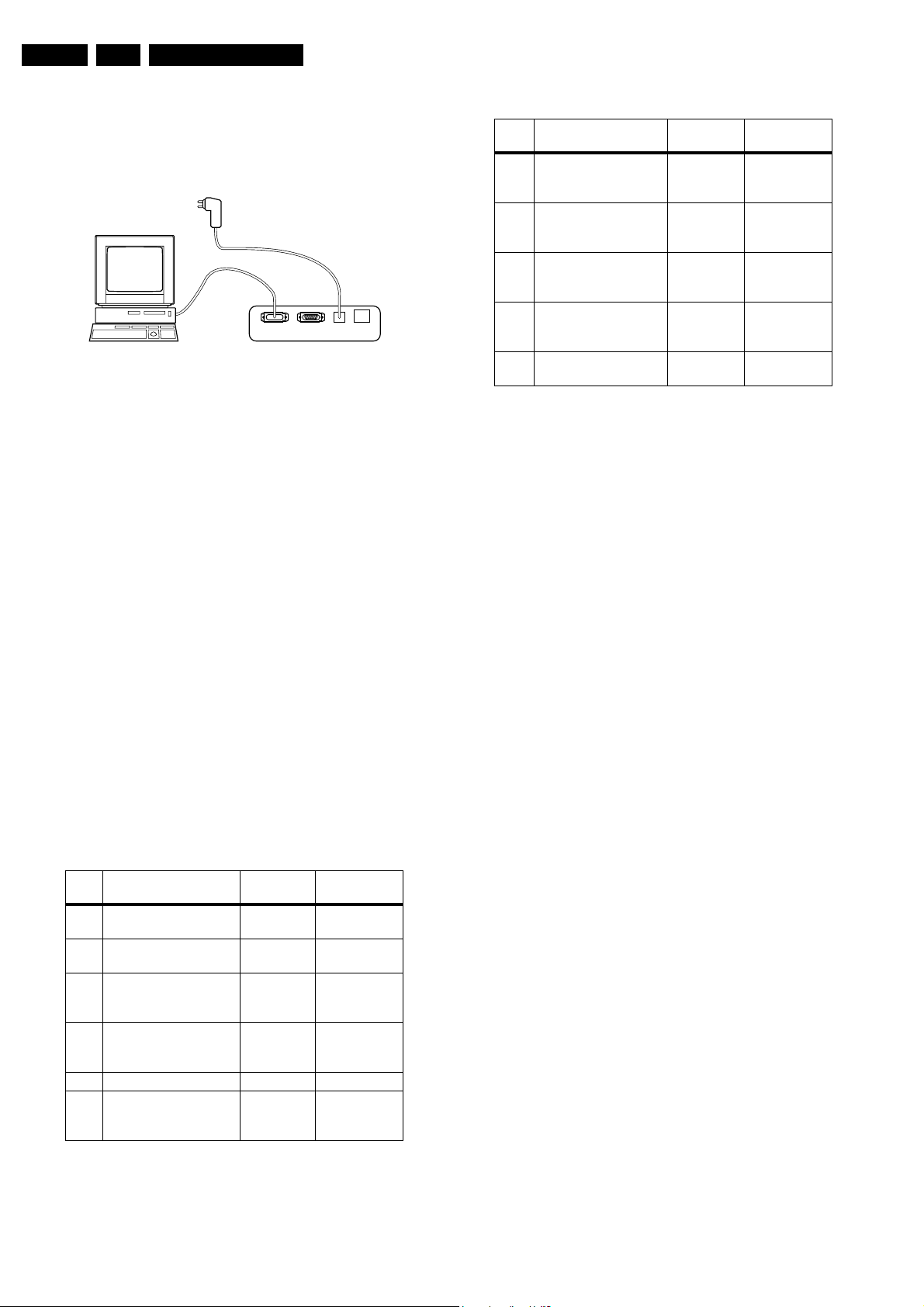
EN 34 F21RE AB5.
Service Modes, Error Codes, and Fault Finding
7. Plug the mains adapter in an mains outlet and switch on the
ComPair interface. The green and red LEDs light up
together. The red LED turns off after approximately 1
second, while the green LED remains lit.
8. Start the ComPair program and read the "introduction"
chapter.
PC VCR I2CPower
Figure 5-2 ComPair set-up
5.4.4 How to Order
ComPair order codes (EU/AP):
• Starter kit ComPair32/SearchMan32 software and
ComPair interface (excl. transformer): 3122 785 90450.
• ComPair interface (excluding transformer): 4822 727
21631.
• Starter kit ComPair32 software (registration version): 3122
785 60040.
• Starter kit SearchMan32 software: 3122 785 60050.
• ComPair32 CD (update): 3122 785 60070.
• SearchMan32 CD (update): 3122 785 60080.
• ComPair interface cable: 3122 785 90004.
5.4.5 Stepwise Start-up / Shut-down
Under normal circumstances, a fault in the power supply, or an
error during start-up, will switch the television to protection
mode. ComPair can take over the initialisation of the television.
In this way, it is possible to distinguish which part of the startup routine (hence which circuitry) is causing the problem.
Stepwise start-up explanation
This is realised via ComPair and is very helpful when a
protection is activated (see also paragraph "Protections").
Table 5-1 Stepwise Start-Up Table
State Mode description Display
LEDs(*)
0 - Low power standby
Red 'on' None
- uP in Standby.
1 - High power standby.
- TV-set in standby.
2 - Supply 'on'.
- Protections 5V2 and
8V6 activated.
3 - Sound ICs initialised.
- Protections FBX and
TUNER activated.
RedFlash
1 time
Orange/
GreenFlash
2 times
Orange/
GreenFlash
3 times
4 Not used in FTV
5 - TV operates.
- Unblanked picture.
Orange/
GreenFlash
5 times
Stepwise shutdown explanation
In the stepwise shutdown mode, state 2 and 4 are skipped.
9V DC
86532027_003.EPS
050898
Enabled
protections
None
67 and 68
Plus 77 and 80
Table 5-2 Stepwise Shut-Down Table
State Mode description Display
LEDs(*)
5 - TV operates.
- Unblanked picture.
Orange/
GreenFlash
5 times
4 - All protections are
'on'.
Orange/
GreenFlash
4 times
3 - Sound ICs initialised.
- All protections 'off'.
Orange/
GreenFlash
3 times
1 - High power standby.
- TV-set in standby.
Red 0.5 HzFlash
1 time
0 - Low power standby.
Red 'on' -
- uP in Standby.
Note (*): When the set is in stepwise mode and, due to
stepping-up, a protection is activated; the set will really go into
protection (blinking LED). The set will not leave the stepwisemode however. By stepping down, the set can be activated
again, until state X where the protection was activated. At state
(X-1) diagnostic measurements can be performed.
5.5 Error Codes
The error code buffer contains all detected errors since the last
time the buffer was erased. The buffer is written from left to
right. When an error occurs that is not yet in the error code
buffer, it is written at the left side and all other errors shift one
position to the right.
5.5.1 How to Read the Error Buffer
It is possible to read out the error buffer in three ways:
• On the screen while in Service Alignment Mode (SAM). If
there is a picture, this is the easiest way to read the error
buffer. In the SAM main menu, the last 10 error codes,
which have occurred, are displayed. The most recently
detected error code is displayed on the left side. Examples:
– 003 000 000 000 000: error code 3 is the last and only
detected error.
– 002 003 000 000 000: error code 3 was detected first
and error code 2 is the last detected (newest) error.
• With the CODE 1 and CODE 2 lines in CSM.
• With ComPair.
5.5.2 How to Clear the Error Buffer
It is possible to clear the error buffer in two ways:
• By selecting the item "reset Error Buffer" in the SAM main
menu.
• By pressing the following key sequence on the remote
control transmitter: MUTE - 062599 - OK.
Note: When the error buffer is full (10 codes), no new errors
can be stored. The set monitors how long every error is stored
in the error buffer. If a false error is in the buffer, it will be
deleted after 50 hours. If an actual error is in the error buffer, it
will be written to the buffer again after 50 hours. This is a
safeguard to ensure that the history of the error codes is stored.
To help ensure that you are not reading false error codes, you
may want to record the contents of the error buffer, reset the
buffer, and see which error codes are generated again by the
set.
Disabled
protections
-
-
-
80, 77, 68, and
67
Page 35
Service Modes, Error Codes, and Fault Finding
EN 35F21RE AB 5.
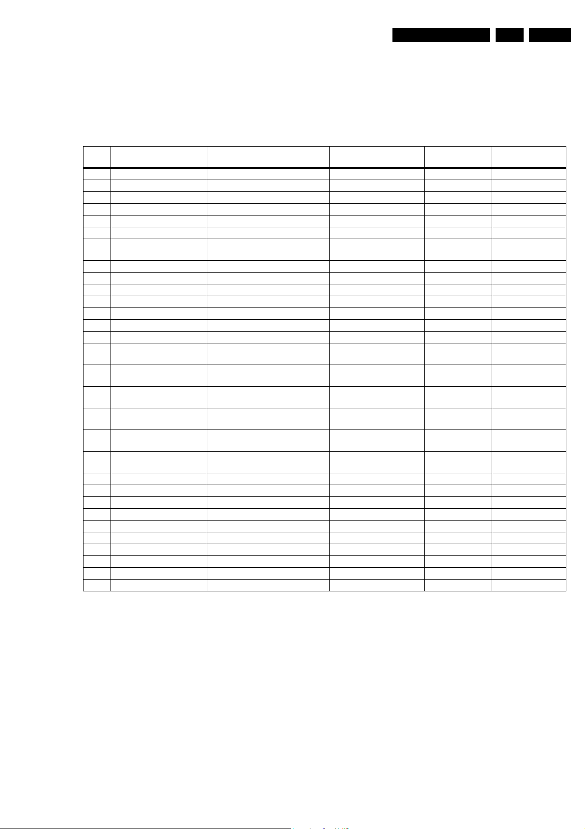
5.5.3 Error Codes
If the set has non-intermittent faults, clear the error buffer
before you begin the repair. This to ensure that old error codes
are no longer present.
Table 5-3 Error Code Overview
Error Device Description Defective item Diagram Defective module
2 ST24E32 or M24C32 Non volatile memory IC7008 K7 Control
3 SAA580x OTC2.5 microprocessor/TXT IC7003 K7 Control
5 UV1316 Tuner U1102 K1 Tuner
10 TEA6415 I/O source select video IC7208 K8 Source select
11 TEA6422 I/O source select audio IC7777 K8 Source select
15 TDA9320 HIP I/O-video processing IC7501 K1 Chroma IF IO
20 TDA9330 HOP video control/deflection proc-
essor
21 TDA9178 (if present) LTP Peaking (TOPIC) IC7402 K6 Video Controller
23 UPD64083 (if present) 3D Comb IC IC7023 C0 3D Comb Filter
25 MSP34xxx ITT sound processor IC7751 K3 Audio Module
27 PCF8574 I/O Expander IC7880 AV8 AV-Interface
30 TEA6415 Video Selection Switch IC7710 AV7 AV-Interface
31 TEA6422 Audio Selection Switch IC7810 AV8 AV-Interface
33 ACEX-EPLD HD signal/sync processing IC7360 AV3 AV Interface
35 UV1316 (if present) FDS Tuner U1102 M1 Video Dual Screen
36 PCF8574 (if present) FDS I/O Expander IC7860 M2 Video Dual Screen
37 SAB9079 (if present) FDS Popov IC7700 M4 Video Dual Screen
38 TDA9320 (if present) FDS HIP2 IC7501 M1 Video Dual Screen
39 M24C04 (if present) FDS NVM IC7991 M1 Video Dual Screen
41 TDA7309 (if present) FDS Headphone IC7620 M5 Video Dual Screen
50 SAA4978 FBX Picnic IC7611 L1 Feature Box
52 T8F24EF (if present) FBX Eagle IC7724 L2 Feature Box
53 SAA4992 FBX Falconic IC7626 L3 Feature Box
65 Slow I2C bus blocked See block diagram Slow I2C Blocked
66 Fast I2C bus blocked See block diagram Fast I2C Blocked
67 Supply 5V 5V2 See block diagram +5V Supply
68 Supply 8V 8V6 See block diagram +8V Supply
77 Featurebox protection FBX prot. +3V FBX Supply
80 Tuner protection Tuner prot. U1102 K1 +8V Tuner Supply
81 UPD64083 (if present) 3D Comb prot. IC7023 C0 3D Comb Filter
If possible, check the entire contents of the error buffer. In
some situations, an error code is only the result of another error
code and not the actual cause of the problem (for example, a
fault in the protection detection circuitry can lead to a
protection).
indication
IC7300 K6 Video Controller
Panel
Panel
Panel
Panel
Panel
Panel
5.6 Protections
The microprocessor (OTC) of the F21R Receiver box remains
active during standby. This because power of the
microprocessor (and the attached memory chip set) is coming
from the 3V3 supply, which is derived from the 5V Standby
circuitry.
Therefore, in both "Power on" as in "Standby" mode, the
microprocessor is connected to this power supply. The
microprocessor controls the "Standby" line for switching "on"
and "off" the main supply. In the standby mode, or in the
protection mode, the "Standby" line will open the contacts of
relay 1400 (diagram PS) via T7401, which results in switching
"off" the mains input to the main supply.
We can divide the chassis protections in two groups:
1. I2C protections: from I2C-busses (fast and slow) or I2C-IC
errors (device errors).
2. OTC input protections.
5.6.1 I2C Protections
During normal operation, some registers of the I2C controlled
ICs are refreshed every 200 milliseconds. During this
sequence, the three I2C busses and the I2C ICs will also be
checked.
Possible protections:
• I2C bus protections. This will take place if the SDA and
SCL are short-circuited to ground or to each other.
• I2C device protections. This can occur when there is a
malfunction in the communication with one specific device,
or if the power supply of the device is missing.
• FBX and/or Tuner circuitry protection. If one of these
circuits does not respond for more than 1 second
Page 36

EN 36 F21RE AB5.
(measured via I2C), the Receiver box goes into protection
mode.
5.6.2 OTC Input Protections
If a protection is detected at an input of the OTC, all protection
inputs of the OTC will be scanned every 200 milliseconds five
times. If the protection on one of the inputs is still activated after
1 second, then the set will go into protection mode.
Possible protections:
• 8V6 and 5V2 protection. The presence of the 8V6 and
5V2 is sensed by the OTC. If the 8V6 and/or 5V2 are/is not
present, then an error code is stored in the error buffer.
Service Modes, Error Codes, and Fault Finding
5.7 Repair tips
5.7.1 How to Deal with a "TV configuration" Situation
It is not easy to access the CSM menu without the
accompanying plasma monitor. Therefore, it is best to retrieve
this information while you still have the complete configuration.
Depending on the fault, the problem may be easily solved.
However, if this is not the case, some of the data recorded
could assist you in the repair.
5.7.2 How to Deal with a "Receiver Box Only" Situation
Without the accompanying plasma monitor, the Receiver box
will go into Standby mode after a few seconds (this monitor
detection is designed to prevent Philips Receiver boxes from
being used with other brands of monitors).
This detection can be overridden in the following way (to use,
for example, a PC monitor):
• Enter the SAM-mode via ComPair (using the "align" key of
the DST simulation mode), or through the HW intervention
of connector 0356 on the SSP (pins 2 and 3). The set will
now operate in SDM. Then short pins 1 and 2 to enter SAM.
• Via navigation in the SAM menu and selecting, you must
follow the this route: "Service Options" - "Miscellaneous" "Stand-alone".
• Toggle "No" to "Yes" and store this change (this means that
a bit is changed in the NVM).
• Now the Receiver box can operate with any monitor (for
example, a PC monitor).
• The Service technician can now perform the diagnosis and
repair (the CSM menu can also be accessed now).
• When the problem is solved, the Stand-alone option bit
should be reset to "No", to return the set to the original
setting.
5.7.3 Miscellaneous Tips/Remarks
• Sometimes, when there is an NVM related error/problem
and the set does not want to start up, it can be helpful to
start the set without the NVM (IC7008 on the IC holder on
the SSP). You can see OSD on the monitor, for a short
time, so you can conclude that much of the circuitry is
working fine.
• If an empty EAROM (permanent memory) is detected, all
settings are set to pre-programmed default (standard)
values.
• To overrule the childlock PIN code, use code "0711".
• When the user settings related to optimal picture and
sound performance are in doubt, one can restore the
default factory settings via: "Settings" - “General” - "Reset
AV settings", and pressing the "OK" key on the remote
control transmitter. This may help correct an incorrect user
setting faster, since the starting point is more clearly
defined (for example, the set will leave the factory with
"DNR" on medium, "Dynamic Contrast" on medium, and
"Sharpness" on 4, etc)..
Page 37
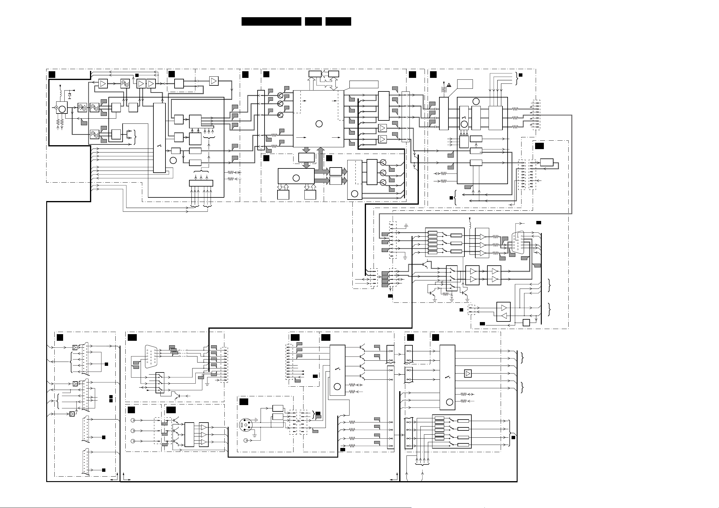
Block Diagrams, Testpoint Overviews and Waveforms
6. Block Diagrams, Testpoint Overviews and Waveforms
Block Diagram (Video)
37F21RE AB 6.
TUNER, IF, I/O,
K1
VIDEOPROCESSING
+5V2
5101
1102
UV1336
79
TUNER 1
ERR
5
154
AGC
3104
3103
SCL-S
SDA-S
CVBS-TXT-OUT
18
K2 CVBS-TER
1
7111
2
10
11
12
15
16
7
17
3
9
IF-VIDEO
1109
IF-AUDIO
1105
1
EF
SOUND
CARRIER
FILTER
7501
TDA9320H
HIP
I5
2
3
I6
62
I3
64
63
I4
CVBS-SC1-IN
CVBS-SC3-IN
Y-CVBS-SC2-IN
SC2-S-IN
CVBS-Y-FRONT
C-FRONT
CVBS-SC2-OUT
CVBS-PIP-DS
RGB-SC1-IN
RGB-SC2-IN
10 12 13 14 26 29
PLL
DEM
QSS
MIXER
AM
DEMO
SIFM
+33V
6101
40.4MHz
ALIGNMENT
11
IF1
5103
I1
64
GROUP
DELAY
AM SOUND
SIF
SIFM
CVBS-TXT-OUT
K7
75021107
EF
TO
AUDIO
BLOCK
DIAGRAM
7561
EF
VIDEO
SWITCH
+
CONTROL
16
18
20
21
23
24
34
32
2D COMB
CF
FILTER
17
12
12
COMB
FILTER
7002 TDA9181
Y
Y
Y
PROC.
C
C
C
PROC.
SYNC
SEPAR.
ERR
15
SCART1 SCART2
1415YC141214
Y/U/V
SWITCH
U
DECODER
PAL
NTSC
SECAM
V-SYNC
PROC.
H-SYNC
PROC.
Y U V
RGB/YUV
MATRIX
G B
R
36 37 38 41 42 43
12
V
Y-DEC
U-DEC
V-DEC
YUV
R G B
FEATURE BOX 7
0361
L1
L1
9
L2
8
L3
7
5
VA
L4
4
HA
L5
L3
7717
MSM54V12222A
7700
7701
7702
3727
3728
FALCONIC
SAA4992
MEMORY
L22
L23
7718
FIELD
2
L6
23
L7
25
L8
26
28
29
MS81V04160
FALCONIC
7719
MSM54V12222A
ADC
7714
ERR
7555
28
49
50
51
61
60
47
46
K8
SOURCE
SELECTION
V3a
V3b
V3c
S1
VA
S2
HA
3531
SDA
SCL
3530
7713
SAA4978H
3x
53
M27C512
MEMORY
7711
FIELD
1
MEMORY
64K
PROM
SIGNAL PROCESSING
PICNIC
ERR
50
SYNC PROCESSING
FIELD
2
LATCH
L2
MS81V04160
V01460M581
EAGLE
7722
FIELD
MEMORY
FIELD
MEMORY
7723
DAC
5
4
7712
74HC573D
OUTPUTS 12, 14, 15, 18, 19
NOT USED IF "EAGLE"
IS PRESENT
12
Y-OUT
Y_EAGLE_E
L9
3x
U-OUT
14
U_EAGLE_E
L10
V-OUT
15
V_EAGLE_E
L11
VD
19
VD_E
L13
HD
18
HD_E
L12
(ONLY PIXEL-PLUS SETS)
7724
T8F24EF
54
3x
63
DAC
73
EAGLE
ERR
52
SDA-S
SCL-S
OUTPUT
FILTER
HD
VD
VIDEO CONTROL+
Y-FEAT
U-FEAT
VDHDVD
VD
(2X)
HD
(2X)
7520
TDA8601T
2
R
6
3
G
7
4
B
8
HD
H_HD_VGA
VD
V_HD_VGA
7540
K6
F1K
2414
F2K
2415
F3K
2416
HD
SDA
SCL
SEE BLOCK
DIAGRAM
CONTROL
CLAMP
CLAMP
CLAMP
CLAMP
CLAMP
CLAMP
7573
GEOMETRY
+8V6
7402
TDA
9178
6
TOPIC
8
9
3304
3303
12
13
3542
3434
20
19
17
16
R
G
B
F4K
F5K
TO
K7
µC
7570
74HTC4053D
5
3
2
1
28
Y
27
U
26
V
30
31
32
23
24
11
10
3-STATE
3-STATE
3-STATE
10
2542
TOPIC
NOT PRESENT
IF "EAGLE"
IS PRESENT
7300
TDA9330
HOP
ERR
21
YUV
RGB
YUV
MATRIX
VFB
HOSD-PIP
16
14
1
4
5
5
TO
K7
CONTROL
S3
+8VV
1550
12
11
10
7575-A:C
741HCT14D
2X BUFFER
7546
ERR
20
Y/U/V
RGB
MATRIX
E/W
DRIVE
V-DRIVE
PROC.
H-DRIVE
PROC.
9
7575 A:C
TSH93
5
6
10
9
12
13
0355
1
3
+
+
+
2
6
RXDO
AV8
-
-
-
K8
SOURCE
SELECTION
L14
0362
9
OR
OR
OR
OR
OR
OR
OR
OR
OR
OR
FEAT_Y
L15
FEAT_U
FEAT_V
VD
HD
Y_EAGLE_E
L24
U_EAGLE_E
L25
V_EAGLE_E
L26
ON
AV4
8
L16
L4
L5
0340
1
2
3
4
5
6
7
8
9
0371
1
2
3
4
VD_E
HD_E
V-FEAT
7
5
4
N.C.
R_VC
1
G_VC
2
B_VC
N.C.
3
4
SDA-S
SCL
5
OUTPUT
FILTER
7704
7703
7733
7731
7735
F521
F525
F529
0371
1
F460
2
F461
3
F462
4
F463
35 36 37
RGB
INSERTION
VD-NEG
LINE DRIVE
3559
7
3560
8
3561
14
7575-B/D
2X BUFFER
3
9
12TXDO
6
CONFIGIDENT
R-TXT
G-TXT
B-TXT
FBL_TXT_OSD
FBSCO
F560
F561
4
8
7460
R
G
B
SEE
BLOCK
A7
DIAGRAM
OSD
CONTROL
0340
1
N.C.
1
2
3
4
5
6
7
8
9
MONITOR
OUTPUT
10
9
8
7
6
F579
6
7545
N.C.
RC_MON
15
14
13
12
11
O.S
2
3
4
5
6
7
8
9
OUTPUT
AV5
SELECTOR
7587
7589
0315
PULSE
1
FORMER
2
3
4
5
6
7
8
9
5
AV7
F578
POWER VALID
10
15
12
11A
11B
11A
FOR
12
FTV1.9
15
11B
FOR
FTV2.1
10
HFB
GENERATOR
3414
40
3413
41
3412
42
3
N.C.
1
N.C.
2
0315
8
0303
3
2
1
F559
H_MON
V_MON
11
5
AV8
F702
C-FRONT
VIDEO-SELECTION
AV7
7710
TEA6415CD
5
IN6
6
IN8
8
IN7
11
IN5
10
IN1
20
IN2
Y-AV-SYNC
ERR
30
4
1
2
3
OUT3
OUT4
OUT1
OUT2
Y-AV-OUT
U-AV-OUT
V-AV-OUT
FBL-YUV
AV8
INPUT/
K2
OUTPUT
17
18
13
14
2
4
7751
F704
CVBS-Y-AV1 FRONT-Y-CVBS Y-CVBS-SC2-IN
7763
F705
C-AV1 FRONT-C
3770
3771
3772
IN-UI-R
IN-UI-G
IN-UI-B
IN-UI-FBL
7765
CVBS-Y-AV2
7767
C-AV2
SDA
SCL
0372
F770
F771
F772
F773
5
7
1
3
5
6
7
8
4, 5, 8
MAIN
SUB
4
8
5
03330333
5
7
0372
1
CVBS-Y-UI
3
C-UI
IN-SC2-CVBS-Y
CVBS-SC4-IN
IN-C IN-R-SC2
5
6
7
8
INPUT RGB FBL SC2
IN-C-IN-R-SC2
14 6
R
G
B
FBL
K8
7209
TDA8601T
2
6
3
7
4
8
7208
TEA6415CD-TR
6
8
10
11
1
5
3
CLAMP
CLAMP
CLAMP
CLAMP
CLAMP
CLAMP
SOURCE SELECT
13
IN8
OUT1
14
OUT2
IN7
17
OUT3
IN1
18
OUT4
15
IN5
OUT5
16
OUT6
IN4
2
4
IN6
ERR
10
IN3
3-STATE
3-STATE
3-STATE
3-STATE
SC2-C-IN
C-7-OUT
7206,7207
CVBS-Y-FRONT
C-FRONT
3288
3289
IN-C-IN-R-SC2
SDA
SCL
12
11
10
9
SC2-R-IN C-IN
SC2-G-IN
SC2-B-IN
SC2-FBL-IN
11
MAIN PATH
12
13
14
15
DOUBLE
WINDOW
PATH
16
9
K1
RGB
SC2
HIP
CL 36532013_013.eps
040403
INPUT/OUTPUT (VIDEO PART)
K2
CVBS-TER
1
3
7
CVBS-SC2-OUT
IN-C-IN-R-SC2
5
6
C-7-OUT
K1,K8
13
FBL
7203, 7204
SCART 1
21
7200
20
CVBS-SC1 IN
19
FBL - SC1 IN
16
15
R
11
G
STATUS 1
8
7
B
FBL
SCART 2
21
7201
20
19
16
15
R
11
G
10
8
7
B
SCART 3
21
20
8
SCART 4
21
20
8
K7
IN-SC2-CVBS-Y
FBL SC2 IN
EASYLINK
STATUS 2
CVBS-SC3-IN
P2-6
K7
CVBS-SC4-IN
P2-5
K7
K7
K7
2, 10
2
4
10
8
8, 4
VGA/HD SELECTION
AV4
0301
H-VGA
13
14
F445
F444
V-VGA
SDA-S
+5V
SD CONNECTOR
SD
(VIDEO PART)
Y
PB
PR
N.C.
N.C.
Y-SD
PB-SD
PR-SD
VGA-IN
1
R-VGA
2
G-VGA
B-VGA
3
7450
74HCT4053D
2
1
12
13
5
3
0304 0304
1
3
5
F440
F441
15
14
SDA-FOCUS
4
AV6
1
F601
3
F621
5
F641
4412
R-HD-VGA
4408
G-HD-VGA
F442
4410
B-HD-VGA
H-HD-VGA
V-HD-VGA
I2C_SCALER_ACTIVE
7453
YPBPR-YUV-MATRIX
-MATRIX-
7603
7623
YPBPR
YUV
MATRIX
7643
Y-AV-SYNC
VGA/HD
AV4
SELECTION
0399
1
2
3
4
5
F439
7607
TSH93
5
6
10
9
12
13
SCL-S
7
8
14
F430
F431
F432
F433
F434
Y-VA-OUT
U-VA-OUT
V-VA-OUT
0398
1
2
3
4
5
6
N.C. N.C.
7
8
9
10
11
FRONT PANEL
FP
SVHS
2
4
CVBS-Y_FRONT
3
1
2
3
4
1
CVBS-Y
7051
7052
7044
16:9
DET.
FRONT
DET.
C-FRONT-IN
F435
Y-SCALER
1
2
F436
3
CVBS-SCALER
4
F437
C-SCALER
5
6
7
N.C.
8
N.C.
9
+5V2
10
+5V2
11
0309
1
2
3
4
5
6
AV8
RESET
SCALER
F438
CONTROL
0309
1
2
3
4
CVBS-Y_FRONT
5
6
F703
Page 38
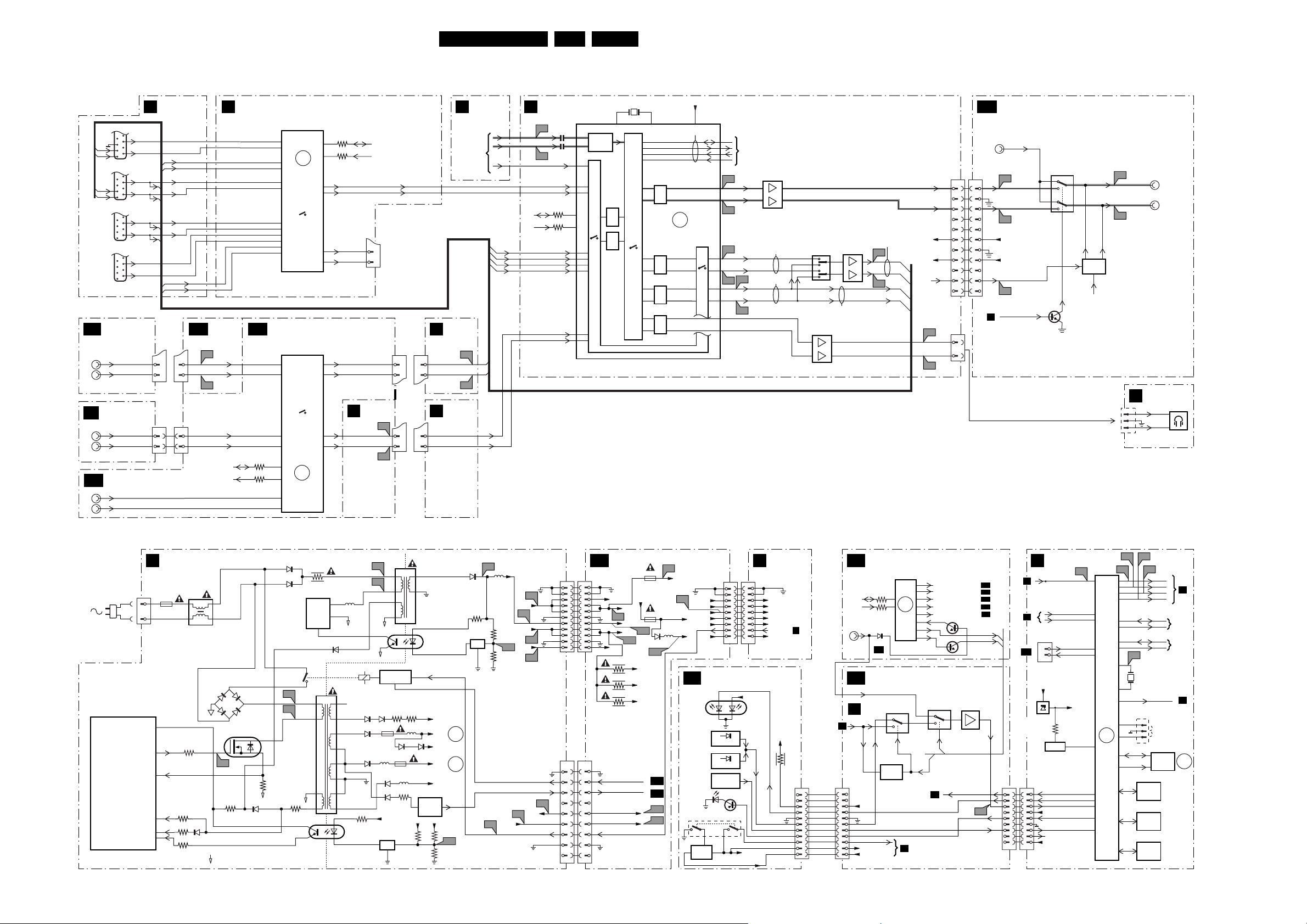
Block Diagrams, Testpoint Overviews and Waveforms
Block Diagram (Audio and Supply)
38F21RE AB 6.
AUDIO
SCART 1
10
L
9
1
R
SCART 2
8
L
7
1
R
SCART 3
1
SCART 4
1
FRONT
FP1
PANEL
SNDL-FRONT
L
SNDR-FRONT
R
SD.
SD
CONN.
SNDL-SD
L
SNDR-SD
R
AUDIO
AV8
AUDIO-L VGA-IN
L
AUDIO-R VGA-IN
R
ERR
+8V6
2
I
S BUS
7
5
N.C.
4
6
7756
A7
R
57
L
56
A8
25
A24
R
51
50
L
A25
R
48
47
L
60
R
59
L
LM833D
5
17R
3
L
TO
CONSTANT
LEVEL
TUNER
A22
SIGNAL
A23
1
5
12
14
5
3
7752
HEF4052
3
3
13
5
TO
SCART 1
7757
MC33178D
71SNDR-HEADPHONE-OUT
SNDL-HEADPHONE-OUT
7758
LM833D
SCART 2
A16
1
R
7
L
A17
R
L
+7V7
R
-7V7
L
7
SOUND
8
ENABLE
9 (2X)
10 (2X)
A14
A15
0344
1
2
3
4
5
6
7
8
9
1
3
1
2
3
4
5
6
7
8
9
1010
1111
03280328
AV8
N.C
N.C
N.C
AV8
CONTROL
AUDI O
AUDIO CENTER IN
SND-CENTER
F811
SNDR-SSP
SNDL-SSP
F812
+7V7
-7V7
SOUND ENABLE
F813
CENTER SELECT
7840 A/B
74HC4053D
12
13
2
1
10 11
7853
14
15
MUTE
POWER VALID
7835
7865
F809
F810
AUDIO-R
MON-OUT
AUDIO-L
MON-OUT
FP
0344
1
2
3
R
L
FRONT PANEL
AUDIO
K2
L
6
3
R
2
6
3
2
6
3
2
6
3
2
9
10
L
3
R
4
L
5
R
6
L
R
1
2
AV7
0309 0309
7
9
0305 0305
3
9
F706
7
9
F709
3
9
K8
VIDEO
SDA
SCL
SOURCE SELECTION
24IN-SC1-SNDR
3822
3824
25
4
23SNDR-SC2-IN
6
20SNDR-SC3-IN
9SNDR-SC3-IN
19SNDR-SC4-IN
10SNDR-SC4-IN
18SNDR-U_I-IN
11SNDR-U_I-IN
AUDIO
7810
TEA6422D
11
18
5
24
28
27
6
23
R2
L2
R1
L1
R3
L3
R4
L4
R5
L5
R6
L6
L1
R6
L1
R2
L3
R3
IN-SC1-SNDL 5
R
L
SNDL-SC2-IN
AV8
7777
TEA64220
ERR
11
ERR
31
R OUT 1
L OUT 1
L OUT 3
R OUT 3
R OUT 2
L OUT 2
L OUT 1
R OUT 1
TUNER +
K1
IF
3866
28
3867
27
13
12
16
17
FDSR-OUT
FDSL-OUT
SNDR-SUB-OUT15
SNDL-SUB-OUT14
A7
SNDL-MAIN-OUT12
SNDR-MAIN-OUT13
0352
VIDEO
SDA
SCL
10
N.C.
11
0373
0373
1
1
SNDR-U-1-IN
3
3
SNDL-U-1-IN
0333
F707
F708
0333
9
9
SNDL-FRONT-IN
11
11
SNDR-FRONT-IN
K8
K2
SEE
BLOCKDIAGRAM
VIDEO
PROC.
SOURCE
SELECT
F821
F827
INPUT
OUTPUT
3
4
5
6
1
2
SOUND
K3
PROC.
I11
SIFM
SIF
I12
AM SOUND
SNDL-SC1-IN 31
SDA
SCL
SNDR-SC2-IN
SNDL-SC2-IN 34
SNDR-SC3-IN
3755
3756
2809
2751
23
25
28
30SNDR-SC1-IN
8
9
33
36SNDR-SC3-IN
37
40SNDL-FROM-IN
39SNDR-FROM-IN
7751
MSP3440
SOUND
DEMODULATOR
ADC
ADC
1751
21
DSP
DIGITAL
SOUND
PROC.
20 45
CLOCK
IN
OUT
WS
DAC
DAC
DAC
DAC
SUPPLY
95 - 264V
7001
MC44603A
CONTROL
CURRENT SENSE
OVERVOLTAGE PROTECTION
VOLTAGE FEEDBACK
POWER SUPPLY STANDBY SUPPLY
PS
0300
1
2
T2,5A
1001
5000
6203
6204
CONTROL
MAIN SUPPLY
6000
3
VCC
OUTPUT
Vdem IN
GBU4J
1
1
3042
3
7
3030
8
3041
6
14
6009
3037
4
6000
2
STP6NC60
G
F013
3016 6007
HOT GROUND HOT COLD
F008
F011
D
S
3012
3013
3014
3015
7200
TNY256
2
3
3200
DRAIN
SOURCE
ENABLE
3
4
6
8
4
3
5003
CONTROL
T12
T11
77 R-TXT
78 G-TXT
79
OSD
TXT
80
86
85
88
87
C3
16
17
104
SERVICE PINS:
119
96
9192SDA
SCL56
T14
T13
B-TXT
F-BL-TXT
SDA-S
2
C0 BUS
I
SCL-S
SDA-F
2
I
C1 BUS
SCL-F
1001
6MHz
STANDBY
0356
1
SAM
2
SDM
3
7008
EEPROM
(NVM)
7002 (ST24E32)
ROM
7001 (HYB3118165)
RAM
7013 (M29W400T)
FLASH
CL 36532013_014.eps
020403
ERR
K6
K1
2
SUPPLY
1
2
3
4
5
6
7
8
9
101110
1
2
3
4
5
6
7
8
9
AV5
03070307
1
2
3
+5V2-FB
4
5
6
7
8
9
11
03060306
1
2
3
4
5
6
7
8
9
N.C.
+5V2
F507
+5VSTBY
+8V6
F509
+33V
3512
3510
3511
POWER-ON
POWER-VALID
+7V7
-7V7
STANDBY
+5VSTB
F516
+8VVA
+8VV
+8VS
1512
T200mA
1513
T200mA
6513
F515
AV7
AV8
F504
F505
F512
5513
+5V
F508
+5VSTBA
+5VSTBD
STANDBY
+5V2-FB
+5V2
+5VSTB
+8V6
+33V
+16V
FP1
6030
TLUV5300
ON/OFF
STANDBY
LED
6025
TSOP2136
6012
TSOP2236
IR LED
ON/OFF
SWITCH
4
2
5V
SWITCH
3
7055 TPS2014P
1
2
3
4
5
6
7
8
9
FRONTPANEL
1
2
IR
RECEIVER
IR
RECEIVER
LOCAL
KEYBOARD
7001
6002
2356
EN
6.7.8
STANDBY
+33V
+8V6
+7V7
+5V2
-7V7
31103111
3113
3114
F026
ERR
ERR
6310
F067
SB340
+5VSTBY
5300
F032
3310
7202
TL431
REF.
2
+5V2
F038
+8V6
3312
3313
3314
F069
+33V
F042
F044
81
68
67
POWER-ON
POWER-VALID
F052
N.C.
+7V7
F054
F056
-7V7
STANDBY
N.C.
5200
F072
F073
5202
5
2.3
4
6010
7401, 7402
1
ACTIVATING
CIRCUIT
2
16
N.C.
6101 6110 3101 3102
15
6103
3109
6106
5103
6107
6108
+8V6
7011
TL431
REF.
1101
T4A
14
13
12
11
10
9
1
2
7002
TCET1103
2
1
4
3
4
3
2
5102
6104 6105
1102
T4A
5104
3107
+8V6
81
7
8
1
2
7101
POWER
VALID
CIRCUIT
7203
TCET1102
+5V2
TUNER (SSP)
K1 AV8
03100310
1
2
3
+5V2-FB
4
+5V2
5
+5VSTB
6
+8V6
7
+33V
8
9
8VF
+5VSTB
RC-FRONT
KEYBOARD
STANDBY
+16V
IR-LED
+5VSTB
+5VSTBY
K7
8VF
3020
1
N.C
2
N.C
3
4
5
6
7
8
9
10
11
AV5
1
2
3
4
5
6
7
8
9
10
11
SDA-S
SCL-S
RC-EXT-IN
AV7
AV5
RC-MON
9-0303
03080308
N.C
N.C
CONTROL
3882
3881
6875
F815
RC-SELECTION
7740-C
5
3
7749
7751
RC-MON
DET.
+8V6
POWER ONPOWER ON
+5VSTB
+5VSTBY
7880
PCF8574AT
I/O
EXP.
15
ERR
14
27
RC-EXT-PRESENT
9
AV5
4
RESET-SCALER
5
HD-VGA-SELECT
6
SYNC-TRISTATE-MON
7
CENTER-SELECT AUDIO
9
FBL-YUV
10
11
12
7884
7740-B
2
4
1
10
RC-FRONT-MON-SEL
21
RC-FRONT-SEL-N
AV4
7881
15
I2C-SCALERACTIVE
ON-OFF-LED
IR-LED
KEYBOARD
7745
7746
AV4
AV5
AV5
AV8
AV6
RC-FRONTMON-SEL
RC-FRONTSEL-N
RC-OUT
F740
TXT & CONTROL
K7
CVBS TXT DS OUT
K8
HFB
K6
VFB
1
2
1
2
3
4
N.C
5
6
N.C
7
8
N.C
9
N.C
0355
1
AV5
3
+5V
STANDBY
+3V3-STANDBY
LF33CV
3043
RESET
03410341
1
2
STBY LED
3
RC5
4
+5V STANDBY
5
IR LED
6
7
KEYBOARD
8
LIGHT SENSOR
9
+8V6
7006
7007
7016
RXD
TDX
7009
7003
T16
SAA5800
5
OTC
83
84
89
90
ERR
3
74
POR
93
113
100
90
107
Page 39
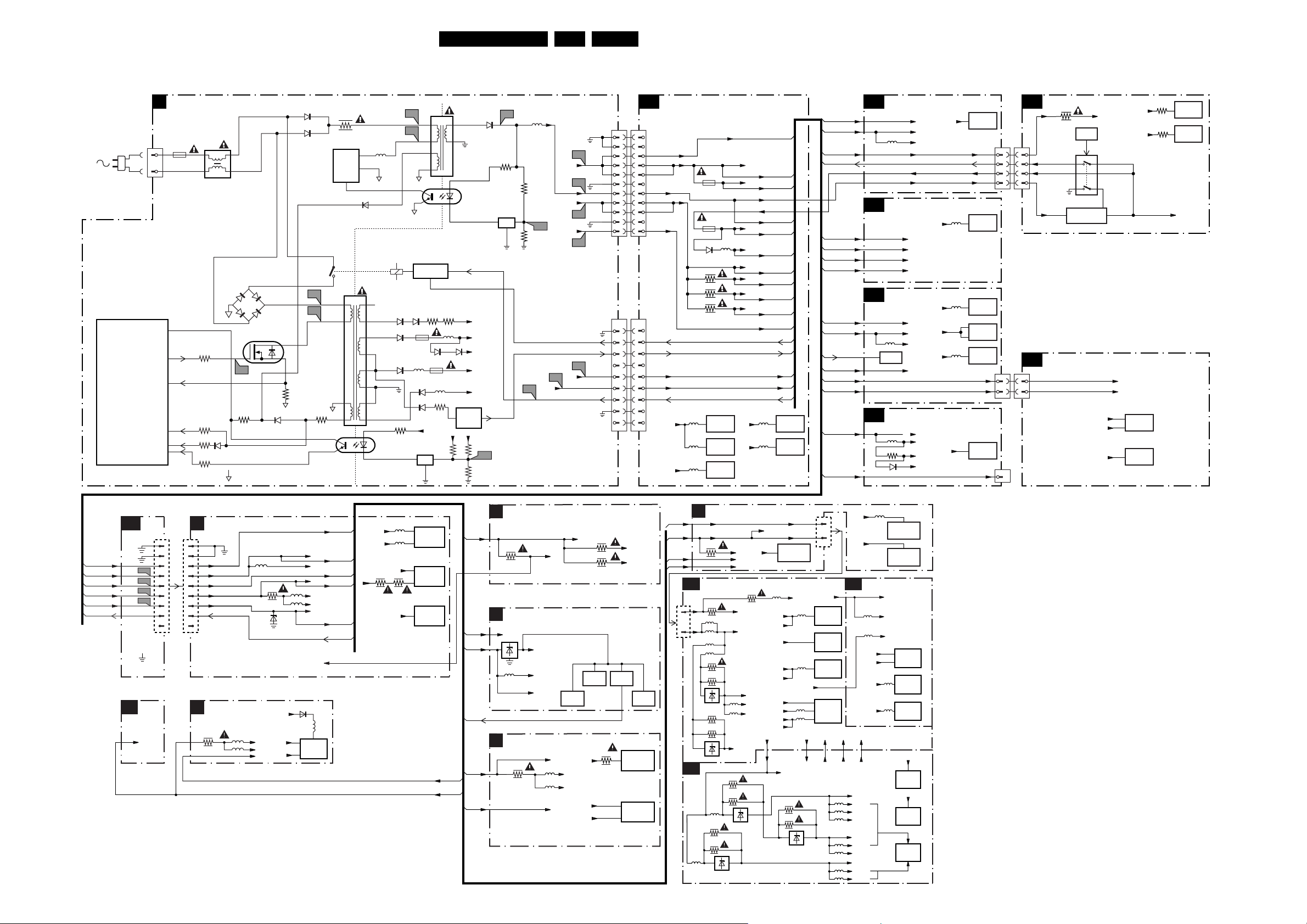
Block Diagrams, Testpoint Overviews and Waveforms
Powerlines Overview
39F21RE AB 6.
95 - 264V
7001
MC44603A
CONTROL
CURRENT SENSE
OVERVOLTAGE PROTECTION
VOLTAGE FEEDBACK
PS
POWER SUPPLY STANDBY SUPPLY
0300
1
2
1001
T2,5A
5000
6203
6204
CONTROL
7200
TNY256
SOURCE
MAIN SUPPLY
2
3
F008
F011
3015
4
3
VCC
OUTPUT
Vdem IN
6000
3
GBU4J
1
1
3042
3
7
3030
8
3041 6009
6
14
3037
4
6000
2
STP6NC60
G
F013
3016
HOT GROUND HOT COLD
6007
D
S
3012
3013
3014
3200
DRAIN
ENABLE
5003
3
4
6
8
AV5
SUPPLY
0307
1
N.C.
2
N.C.
3
4
5
6
7
8
9
10
11
1
2
3
4
5
6
7
8
9
+5V2-FB
+5V2
N.C.
N.C.
+33V
03060306
N.C.
N.C.
N.C.
N.C.
+8VV
+5VSTBD
T200mA
+5VSTBY
+8V6
POWER-ON POWER-ON
POWER-VALID POWER-VALID
+7V7
-7V7
STANDBY STANDBY
5520
5550
16
T200mA
1
4
1512
1513
6513
3512
3510
3511
7520
TDA8601T
7550
OP. AMP
7545
ONE SHOT
5513
+5V2-FB
+5V
+5STBA
+5V2
+5V
+5VSTBA
+5VSTBD
+8V6
+8VVA
+8VV
+8VS
5575
5570
+5VSTBY
+5VSTB
+5VSTBY
+5VSTBA
+5VSTBD
+7V7
-7V7
14
16
+5V2
+8V6
+8VVA
+8VV
+8VS
+33V
+5V
7575
BUFFER
7570
SWITCH
+5VSTBA
+8VVA
1X
+8V6 +8V6
POWER-ON POWER-ON
1X
1X
1X
3X
1X
2X
1X
1X
1X
1X
1X
1X
1X
1X
1X
+5VSTB
+5VSTBY
+5V
+8VV
+5VSTBA
+5VSTBD
+5VSTBA
+8VS
POWER-VALID
+5VSTBY
+7V7
-7V7
+8VV
+8V6
7
8
1
2
7101
7203
TCET1102
POWER
VALID
CIRCUIT
+5V2
6310
SB340
STANDBY
+33V
+8V6
+7V7
+5V2
-7V7
3110
F026
3113
3114
F067
3310
7202
TL431
REF.
+5VSTBY
5300
+5V2
3312
+5VSTBY
+8V6
81
F069
2
3313
3314
F056
+33V
POWER-ON
POWER-VALID
+7V7
F054
-7V7
STANDBY
F032
F038
F042
F044
F052
N.C.
N.C.
0307
1
2
3
4
5
6
7
8
9
10
11
1
2
3
4
5
6
7
8
9
5200
F072
2
F073
1
5202
5
2.3
4
6010
16
N.C.
15
14
13
12
11
10
9
1
7002
TCET1103
2
4
3
4
3
7401, 7402
1
ACTIVATING
CIRCUIT
3
6101 6110 3101 3102
6103
6106
3109
5103
1101
T4A
6107
6108
7011
TL431
REF.
6104 6105
1102
T4A
5104
3107
+8V6
3111
81
2
5102
+8V6
AV7
VIDEO + RC + SELECTION
5710
+5VSTB
+5VSTBY
AV4
VGA/HD SELECTION
+5V WORDT NIET GEBRUIKT
+8VV WORDT NIET GEBRUIKT
+5STBA
+5VSTBD WORDT
NIET GEBRUIKT
AV8
AUDIO + CONTROL
+5VSTBA
+8VS
5810
+8VTEA
AUDIO
MUTE
+5VSTBY (TO 4866)
AV6
YPBPR-YUV-MATRIX
5655
3666
6666
+5VSTBA
+8VVA
+8VT
+5VSTBA
+5VSTBA
+8VV
+8D
+Vref 3
+Vref 4
+8VTEA
+8VS
+8TV
+5VSTBY
+8D
+8V6
+5VSTB
5450
5880
5840
FP
FRONT PANEL
7710
9
SWITCH
0308
7450
16
SWITCH
7880
I/O EXP.
3
7810
SWITCH
26
7840
SWITCH
0328
+7V7
-7V7
4
7607
OP. AMP
0304
+8V6
0308
3
3
9
9
10
10
11
11
K3
0328
6
6
8
8
10
N.C.
3020
POWER ON
+5VSTB
+5VSTBY
2, 3, 4
SOUND PROCESSING
ON/OFF
1006
23
65
7055
5V SWITCH
+7V7
-7V7
+7V7
+8VF
4
6, 7, 8
+7V7
-7V7
16
17
8
+5VSTB
+5VSTB
7752
SWITCH
7758
OP. AMP
3025
3026
2
2
6025
RC. REC
6012
RC. REC
+5VSTB
+5V2-FB
+5V2
+5VSTB
+8V6
+33V
STANDBY
B11
B12
B13
B14
COLD GROUND
CO
+5V2
0310
INPUT/OUTPUT
TUNER, IF
K2
K1AV5
VIDEO PROC.
0310
1
1
1
2
2
2
3
4
5
6
7
8
9
3
3
4
4
5
5
6
6
7
7
8
8
9
9
N.C.N.C.
K3
3750
+5V2-FB
+5V2
+5V-Standby
+8V6
+33V
STANDBY
SOUND
PROCESSING
5751
5752
5101
+5DA
+5DB
+8V6
3538
+5DB
+5DA
6101
-/33V
+8V6
5501
5502
(TO C-7111)
67
11
26
6757
7551
MSP3410D
+5V2-FB
+5V2
+5V2
+5V
+5V-STBY
+8V6
+8V6
+8Va
+8Vb
+33V (TO 91102 TUNER)
+33V
STANDBY
xxx
5753
45
1x
4x
1x
+8V6
4x
1x
1x
+5V2
+5V2
3150
+33V
+8Va
3151
5559
5562
22
7
9
7
11
7560
SAA4961
TUNER
UV1316
1102
7501
TDA9320H
HIP
+8V6
+5V2
+8V6
+5V2
+5V STBY
Standby
+8V6
+5V2
3147
TXT & CONTROL
K7
+5V2
7009
+3.3V-STBY
5002
+5V-Standby
+5V-STBY
VIDEO CONTROL & GEOMETRY
K6
3300
5301
5302
xxx
+8V6
+5V2
7001
RAM
+8VS
+8VR
+8V6
3225
TO C-7201
3204
TO C-7200
111
22
7002
7003
ROM
3434
µC
104
FLASH
7402
20
TDA9178
TOPIC
17
7300
TDA9330H
39
HOP
1
+8V6
+8VS
+8VR
7013
+5V2-FB
+8V6
+33V
+5V2
23
0362
L1
1
2
L2
K8
FEATURE BOX
+8V6
5703
+5V2
-FB
5704
5706
5705
EAGLE
5728
SOURCE SELECTION
+5V2-FB
+8V6
3290
Vdd
+33V
+5V2
3857
3711
TO
3722
3723
3724
+5VA
3737
3809
+3.3VA
5715
7725
3808
3780
5713
+3.3VFM
+3.3P
+2.5VB
7720
7705
7706
3739
3810
5723
3807
3786
0362
2
+5V2-FB
+8V6
9
Vdd
TEA6415CD
5731
+5VA
+3.3VA
+3.3VFM
+5VA
+3.3VA
+3.3P
+3.3VA
+5VA
+3.3VA
+5VA
3825
3824
7208
7739
+8.6VF
5711
5710
5714
5712
+8V6
+2.5VB
+8.6VF+5VA
+8.6VF
123
149
20
32
31
1
7712
LATCH
7714
FIELD
MEMORY 1
7711
PROM
7713
PICNIC
+1.5VC
+1.5VC
+2.5VD
+2.5VD
5736
5727
5726
5730
5729
5725
5724
+8V6
Vdd
L3
+3.3VC
+3.3FE
+3.3FC1
+3.3FC2
+1.5VC
+1.5VCC
+1.5VA
+2.5VD
+2.5FDA
+2.5FDD
+2.5FB
+3.3FA
+3.3V A
+3.3VA
+3.3VC
+3.3VC
5757
FALCONIC
5719
5718
+3.3VA+3.3VA
+3.3FA
+2.5FB
143
5716
5717
3
7777
TEA6422D
1
7209
TDA8601
7718
FALCONIC
7717
FIELD
MEMORY 2
7719
FIELD
MEMORY 3
+3.3FC1
7722
FIELD
MEMORY5
+3.3FC2
7723
FIELD
MEMORY4
7724
EAGLE
CL 36532013_015.eps
110303
Page 40
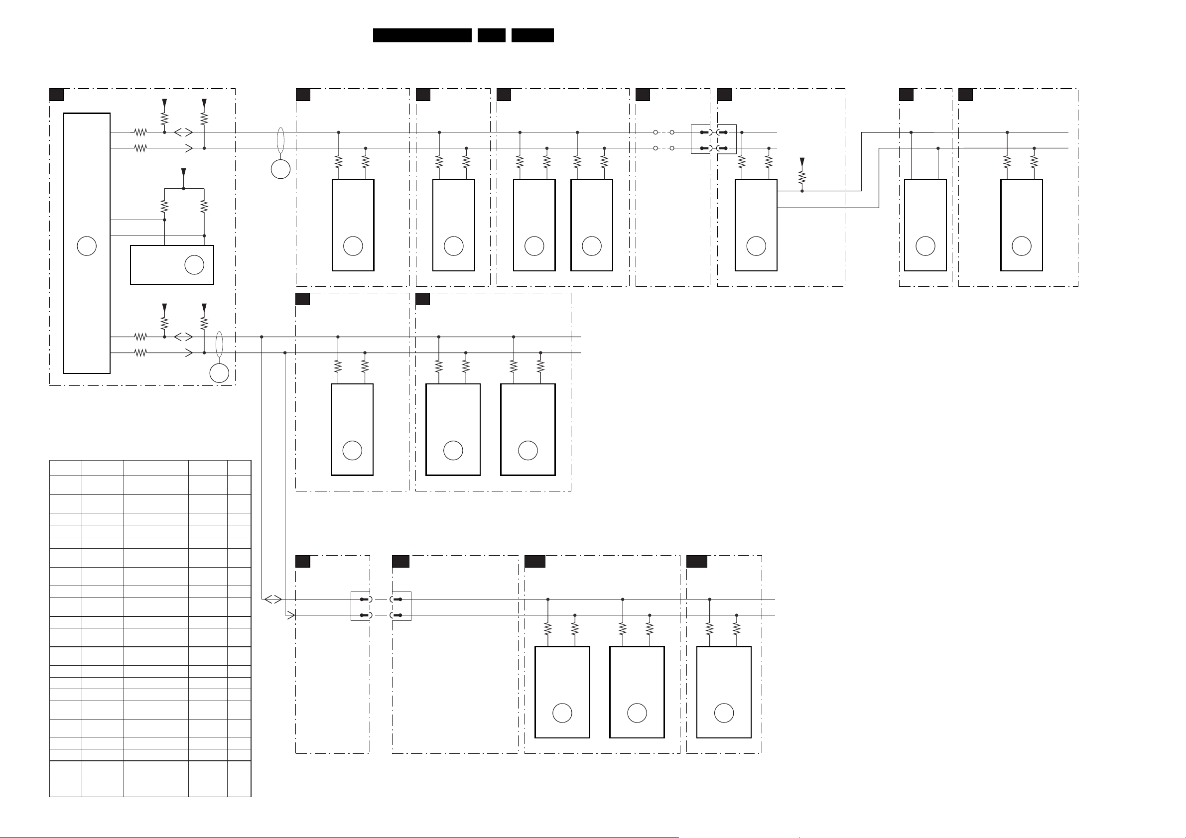
Block Diagrams, Testpoint Overviews and Waveforms
I2C-IC’s Overview
40F21RE AB 6.
TXT & CONTROL
K7
7003
SAA5801
SET
PROCESSOR
ERR
+5V2
3033-C5
88
3033-D6
87
+3V3-STANDBY
91
SDA
92
SCL
3
ST24E32
EEPROM
3033-B7
86
3033-A8
85
56
7008
(NVM)
+5V2
+5V2
3036-C6
3075 3076
3036-A8
ERR
2
+5V2
3036-B7
3036-B5
ERR
65
SDA-F
SCL-F
SDA-S
SCL-S
ERR
66
TUNER, IF, SOURCE
K1
SELECTION & VIDEO PROC.
3531
47 46
7501
TDA9320H
HIP
ERR
15
TUNER, IF, SOURCE
K1
SELECTION & VIDEO PROC.
3104
5
3530
3103
4
SOUND PROC.
K3
8
MPS3440
DECODER
SOURCE
K8
SELECTION
2
3755
7751
NICAM
ERR
25
3288
3756
9
3289
4
VIDEO CONTROL & GEOMETRY
K6
3432
3433
14
11
7402
TDA9178
TOPIC
ERR
3866
28
21
27
TDA9330H
3867
3304
11
7300
HOP
ERR
20
10
3303
SOURCE
K8
SELECTION
4402
4403
0361
2
1
FEATURE BOX
L1
0361
SDA-D SCL-D
2
1
5
SAA4978H
PICNIC
SDA-F
SCL-F
3710
7713
ERR
50
3709
4
FALCONIC
L3
+5VA
3758
1
2
SN-DA
SN-CL
26 27
7718
SAA4992
FALCONIC
ERR
53
L2
EAGLE
4741-B7
SN-DA-E
26
32
7724
T8F24EF
EAGLE
ERR
52
4741-C6
SN-CL-E
Error Device Description Def. item Diag
2 ST24E32 NVM (Non Volatile
3 SAA5800 OTC2.5
5 UV1336 Tuner U1102 K1
10 TEA6415 I/O select video IC7208 K8
11 TEA6422 I/O select audio IC7777 K8
15 TDA9320 HIP I/O-video
20 TDA9330 HOP video
21 TDA9178 LTP Peaking IC7402 K6
25 MSP3440 ITT sound
27 PCF8574 I/O select audio IC7880 AV8
30 TEA6415 Video selection
31 TEA6422 Audio selection
50 SAA4978 FBX PICNIC IC7611 L1
52 T8F24EF EAGLE IC7724 L2
53 SAA4992 FBX FALCONIC IC7626 L3
65 Slow I2C
bus blocked
66 Fast I2C
bus blocked
67 Supply 5V 5V2
68 Supply 8V 8V6
77 Feature box
protection
80 Tuner
protection
memory
microprocessor
processing
control/geometry
processor (MSP)
switch
switch
FBX-PROT L1
TUNER-PROT
IC7008 K7
IC7003 K7
IC7501 K1
IC7300 K6
IC7751 K3
IC7710 AV7
IC7810 AV8
K7
K7
K8
SELECTION
NOTE 1)
1102
UV1316
TUNER
ERR
5
AV4
0371
3
4
MESSAGE BASED ERRORS ARE
RETRIEVABLE VIA COMPAIR TOOL
VIA SET, IN THE ERRORBUFFER
FOLLOWING ERRORS CAN OCCUR:
0371
TEA6415CD-TR
ELECTRONIC
VGA/HD SELECTIONSOURCE
3
4
7208
SWITCH
ERR
10
7777
TEA6422D
ELECTRONIC
SWITCH
ERR
11
AV8
ELECTRONIC
AUDIO + CONTROL
3822
3824
28
27
7810
TEA6422D
SWITCH
ERR
31
3882
15
7880
PCF8574AT
I/O
EXPANDER
ERR
27
14
3881
VIDEO
AV7
SELECTION
3722
2
7710
TEA6415CD-TR
ELECTRONIC
SWITCH
ERR
30
3723
4
CL 36532013_016.eps
020403
Page 41
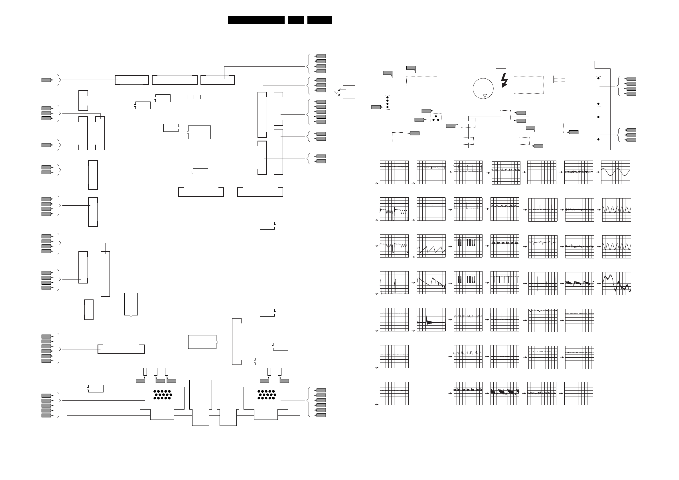
Block Diagrams, Testpoint Overviews and Waveforms
Testpoint Overviews (AV + PS)
AV interface panel (AV) Power supply panel (PS)
0341
3
F740
0340
F521
F525
F529
0315
F585
0373
F821
F827
0371
F460
F461
F462
F463
0333
F704
F705
F707
F708
0372
F770
F771
F772
F773
3
5
7
1
1
3
1
2
3
4
5
7
9
11
5
6
7
8
0355
0315
0340
28
19
82
0370
28
19
71
0373
0371
62
71 26
11
10
0372
0333
91
2
1
153
24
Y/C CVBS SELECTION
0341
82
19
7740
RC-SELECTION
7710
0308
111
210
ONE-SHOT
7545
VGA/HD SYNC
SWITCH
7450
1519
1.9
2.3
JUMPERS
I/O EXPANDER
7880
SYNC SWITCH
111
210
0309
19
28
7570
0399
N.C. N.C.
19
0306
0328
0307
0310
1 9 10 2
0398
111
210
MONITOR OUTPUT SWITCH
7520
CENTRE / LR SELECTION
7840
210
2 8 11 1
11182
41F21RE AB 6.
0309
3
F702
5
F703
0309
7
F706
9
F709
0328
1
F811
3
F812
10
F813
0306
2
F501
3
F502
4
F503
5
F504
6
F505
0307
4
F507
7
F516
0310
5
F508
6
F509
0300
F008
F008
50V / div DC
F011
100V / div DC
F012
6000
45
1
5µs / div
5µs / div
F012
20V / div DC
5µs / div
F013
2V / div DC
5µs / div
F016
1
4
7200
8
F071
910 16
7001
F011
F013
F073
F067
1V / div DC
10µs / div
F069
500mV / div DC
10µs / div
F071
1V / div DC
10µs / div
F072
1V / div AC
2ms / div
F073
(COPPER TRACK SIDE)
18
7000
D
GS
56
2
F072
F460
2V / div DC
20µs / div
F461
2V / div DC
5ms / div
F462
2V / div DC
5ms / div
F463
2V / div DC
5ms / div
F521
2005
+
USE (-) LEAD AS HOT
MEASURE GROUND
5200
101
41
7203
23
-
34
F559
1V / div DC
20µs / div
F560
1V / div DC
20µs / div
F561
1V / div DC
20µs / div
F578
2V / div DC
20µs / div
F579
7002
HOT COLD
F016
12
F024
41
7202
USE HEATSINK AS COLD
5003
MEASURE GROUND
F067
85
41
F069
F621
500mV / div DC
20µs / div
F641
2V / div DC
5ms / div
F702
500mV / div DC
20µs / div
F703
50mV / div DC
20µs / div
F704
6103
AC
7011
85
F707
20mV / div AC
F708
20mV / div AC
F709
20mV / div AC
F770
20mV / div DC
F771
F026
2ms / div
2ms / div
200µs / div
20µs / div
0307
1
11
0306
1
9
F811
500mV / div AC
200µs / div
F812
500mV / div AC
200µs / div
F821
20mV / div AC
200µs / div
F827
20mV / div AC
200µs / div
0307
3
F032
7
F038
8
F042
11
F044
0306
5
F052
6
F054
7
F056
0304
F601
F621
F641
F660
F661
F670
0301
F440
F441
F442
F444
F445
1
3
5
7
9
11
YPbPr / RGB MATRIX
1
2
3
13
14
111
210
3446
F444 F445
7607
3447
3580
F580
51
10 6
15 11
0301 0303
AUDIO INPUT SELECTION
7810
0302
0313
RGB OUTPUT BUFFER
7550
10 2
11 1
7575
3579
3578
F579 F578
51
10 6
15 11
0303
1
F559
2
F560
3
F561
13
F578
14
F579
9
(MEASURE OTHERSIDE)
F580
2V / div DC
5µs / div
F024
2V / div DC
10µs / div
F026
500mV / div DC
10µs / div
100V / div DC
10µs / div
(COMPONENT-SIDE)
2V / div DC
20µs / div
F525
2V / div DC
20µs / div
F529
2V / div DC
20µs / div
2V / div DC
5ms / div
F580
2V / div DC
20µs / div
F601
500mV / div DC
20µs / div
500mV / div DC
20µs / div
F705
2V / div DC
20µs / div
F706
20mV / div AC
200µs / div
2V / div DC
20µs / div
F772
2V / div DC
20µs / div
F773
2V / div DC
20µs / div
CL 36532013_025.eps
110303
Page 42
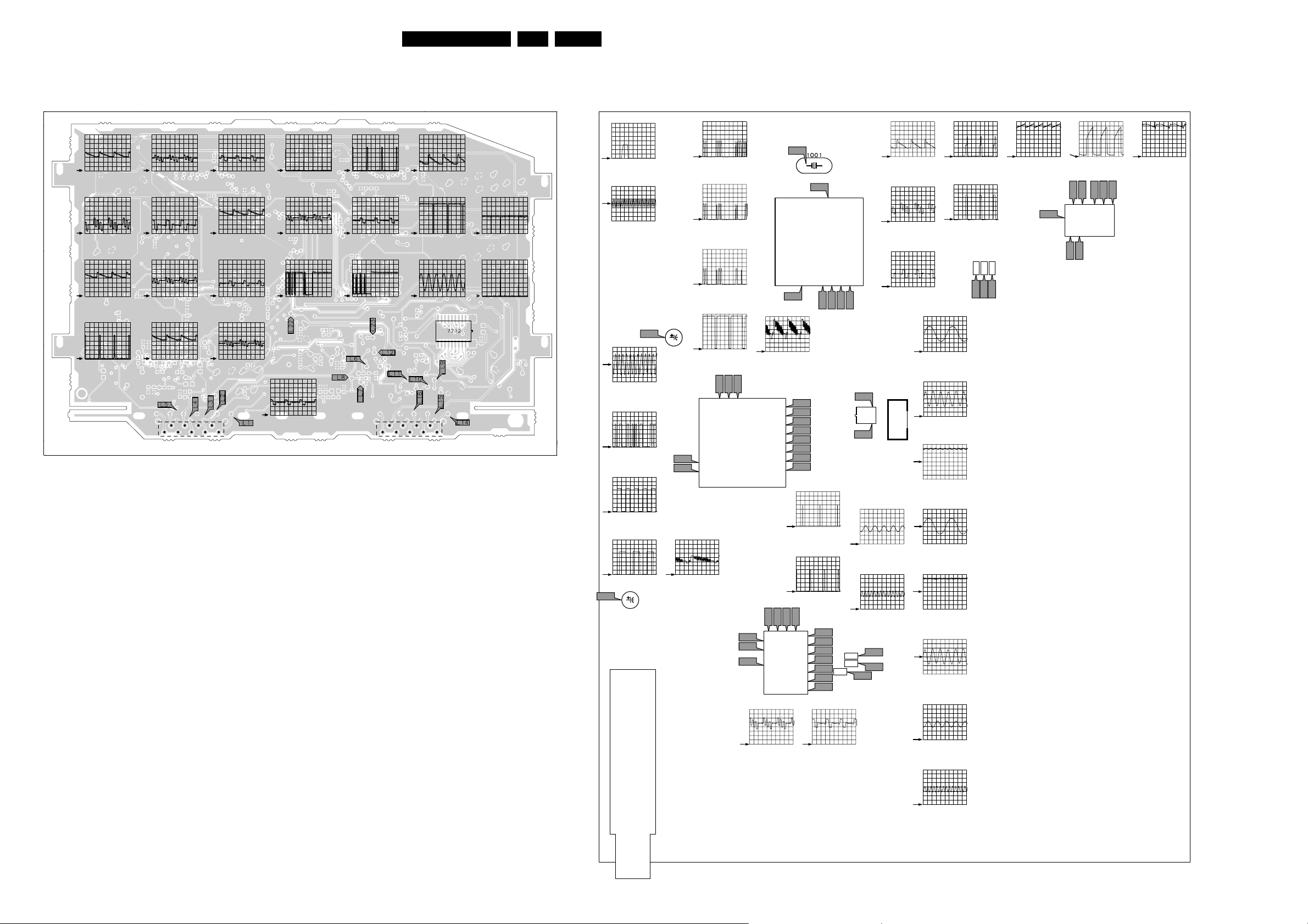
Block Diagrams, Testpoint Overviews and Waveforms
Testpoint Overviews (K + L + M)
L1
L2
L3
42F21RE AB 6.
Small signal panel (K)FBX panel (L)
L4
L5
L6
C1 Reset/c-7007
T11 R/77-7003
F1K
Y-OUT/19-7402
S3 SC/9-7300
S6 Frame/6-7300
S7 SS-Drive
S8 EW/3-7300
1 V / div DC
20µs / div
L7
500mV / div DC
20µs / div
L14
1 V / div DC
10µs / div
L23
1 V / div DC
20µs / div
1 V / div DC
20µs / div
L8
500mV / div DC
20µs / div
L15
1 V / div DC
10µs / div
L24
1 V / div DC
10µs / div
0361
1
1 V / div DC
20µs / div
L9
1 V / div DC
10µs / div
L16
1 V / div DC
10µs / div
1 V / div DC
10ms / div
L10
1 V / div DC
10µs / div
L17
1 V / div DC
100µs / div
L25
1 V / div DC
10µs / div
9 1
L26
1 V / div DC
10µs / div
(COPPER-SIDE)
1 V / div DC
20µs / div
L11
1 V / div DC
10µs / div
L18
1 V / div DC
100µs / div
0362
500mV / div DC
20µs / div
L12
500mV / div DC
10µs / div
L19
500mV / div DC
50ns / div
9
L13
200mV / div DC
5ms / div
L22
500mV / div DC
5ms / div
CL 16532149_096.eps
191201
1V / div DC
10ms / div
C3
6MHz/2016/1001
20mV / div AC
0.5µs / div
I12
SIF/Pin5-7501
0.2V / div DC
5µs / div
I13
I2S-DSP-IN/5-7751
1V / div DC
5µs / div
I14
I2S-CL/7-7751
1V / div DC
5µs / div
I15
I2S-WS/6-7751
1V / div DC
10µs / div
I1
I1 +1V4 DC
C2 +3V3 DC
C2
I12
I13
I7 B7502
1V / div DC
10µs / div
0.2V / div DC
1µs / div
T12 G/78-7003
0.2V / div DC
1µs / div
T13 B/79-7003
0.2V / div DC
1µs / div
T14
Fading/80-7003
0.2V / div DC
10µs / div
I15
6
9
MSP
23
25
I14
I13
7751
I5
I6
I7
V3b Uout/50-7501
31
60
T16 CVBS
0.2V / div DC
20µs / div
614 1/685
6010
59
57
56
51
50
48
47
44
4343
I4
I3
61 606364
2
HIP
3
7501
13
C3
T16
7003
uC
C1
/5-7003
A20
A21
A7
A8
A24
A25
A22
A23
S1 VA/P61-7501
1V / div DC
5ms / div
S2 HA/P60-7501
1V / div DC
20µs / div
S2
S1
V3c
51
V3b
50
V2a
49
V2d
40
V1c
38
V1b
37
V1a
36
V3c Vout/51-7501
OTC
T11
T12
2510
T13
7757
2512
2511
1530
120
91
9078 79 807761 74
T14
A20a
A21a
A24
A25
V2a
F2K
F3K
1
2
SC2-R/51-7751
1V / div DC
0.5ms / div
SC2-L/50-7751
1V / div DC
0.5ms / div
V2c
V3b
0.5V / div DC
10µs / div
U-OUT/17-7402
0.5V / div DC
10µs / div
V-OUT/16-7402
0.5V / div DC
10µs / div
2
31
A7 (ssp)
0.5V / div
0.2ms / div
A8 (ssp)
0.5V / div
0.2ms / div
A20
R/60-7751
20mV / div DC
1ms / div
A20a
2V / div
0.2ms / div
A21
L/59-7751
20mV / div DC
1ms / div
A21a
2V / div
0.2ms / div
A22
SC1-R/48-7751
1V / div DC
10µs / div
S4 HFB/13-7300
1V / div DC
10µs / div
2414
2415
F1k
F2k
2416
F3k
0.1V / div DC
5ms / div
S4
12
13
22
23 24
S3
7300
S3
S7
1V / div DC
10µs / div
S8S6S6
S7
HOP
33
0.5V / div DC
10µs / div
1238911
34
TUNER
0.5V / div DC
20µs / div
0.5V / div DC
20µs / div
(COMPONENT-SIDE)
1V / div DC
0.5ms / div
A23
SC1-L/47-7751
1V / div DC
0.5ms / div
CL 36532013_017.eps
050303
Page 43
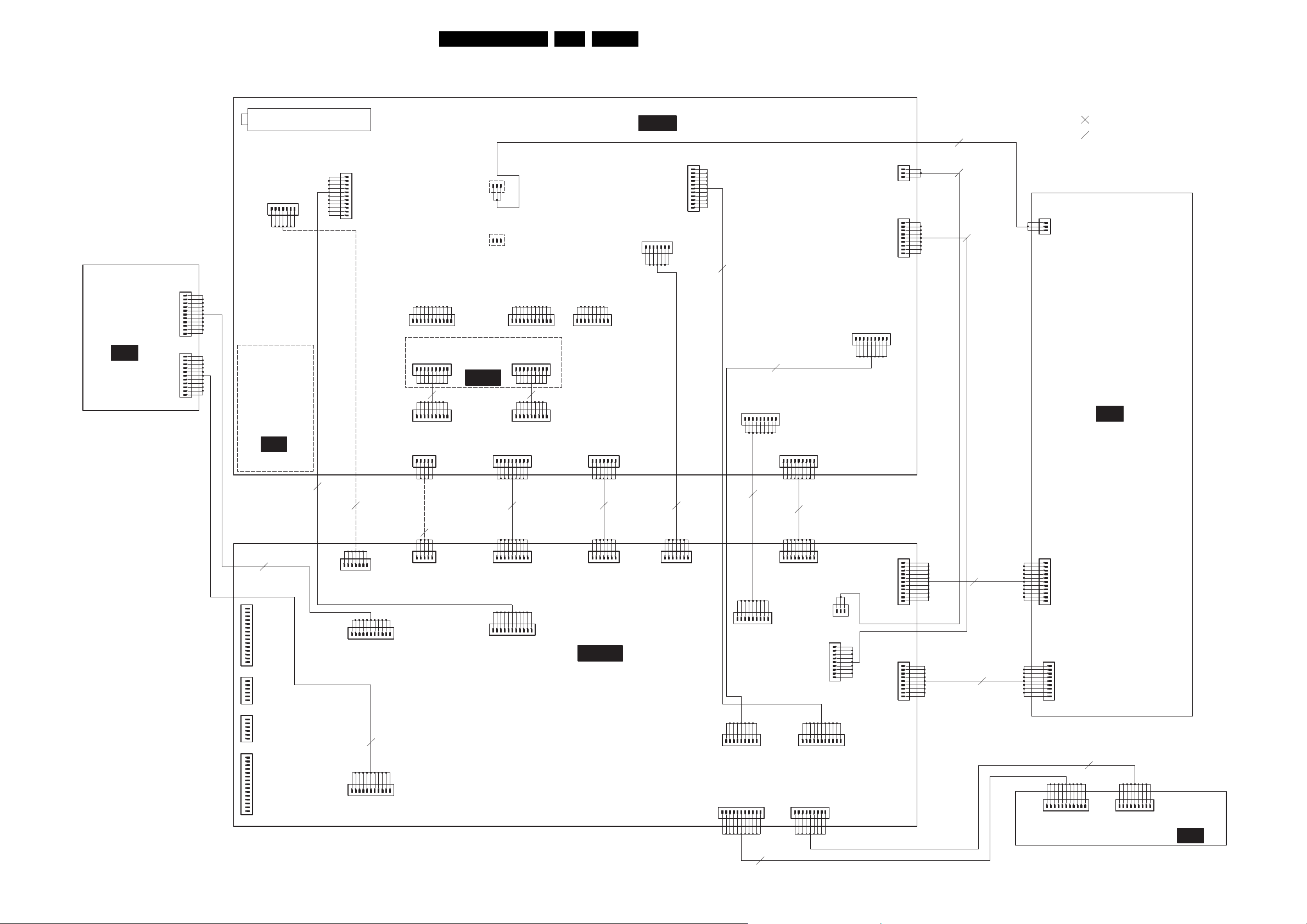
Block Diagrams, Testpoint Overviews and Waveforms
Wiring Diagram
43F21RE AB 6.
SD-panel
Europe
DIAGRAM
SD
1037
Y_SD
GND
PB_SD
GND
PR_SD
GND
CVBS_Y_EXT3
GND
C_EXT3
+8V6
16:9_EXT3
GND
SNDL_SD
GND
SNDL_EXT3
GND
SNDR_EXT3
GND
SNDR_SD
GND
SNDR_HD
0304
XXX
0305
XXX
SMALL SIGNAL PANEL
+5V2_FB
+8V6
GND
VD
HD
GND
pos 8062
SS-panel
11
FEAT_Y
FEAT_V
FEAT_U
9
9
1020
XXX
XXX
XXX
1
0353
TUNER
0333
1
16:9_ARFRONT
NC
GND
GND
CVBS_Y_FRONT
GND
FBL_SC1_IN
IN_SC1_B(U_OUT)
IN_SC1_R(V_OUT)
IN_SC1_G(Y_OUT)
GND
+8V6
CVBS_SC1_IN
0385
1
1
11
1
XXX
7
COMB FILTER
11
CF-panel
7560
FRONT_C
GND
SNDL_FRONT_IN
FRONT_DETECT
SNDR_FRONT_IN
11
XXX
USA and A/P
0351
1
0361
0361
SCL_S
1
9 Fold
1
NC
SDA_S
HA
VA
GND
pos 8061
Y_DS_!Fh
V_DS_!Fh
U_DS_!Fh
11
XXX
FEATURE BOX (7)
FB-panel
1022
DIAGRAMS
XXX
99
L1 : 3
XXX
0348
0348
XXX
3
1
1
3
XXX
1
0352
0362
1
9 Fold
1
0362
DIAGARAM
1
15
1
6
1
6
1
15
XXX
0302
XXX
XXX
0303
XXX
11 Fold
301
0313
CF
pos 8004
R_VGA
G_VGA
B_GVA
NC
NC
GND
GND
GND
NC
GND
NC
NC
H_VGA
V_VGA
NC
SNDR_VGA
SNDL_VGA
SND_CENTER
GND
GND
GND
SNDR_MON
SNDL_MON
RC_EXT
GND
GND
GND
R_MON
G_MON
B_MON
NC
GND
GND
GND
GND
RC_MON
GND
CONFIG_IDENT
TXDO
H_MON
V_MON
RXDO
11 Fold
VGA-INPUT
in/out
Audio VGA
Centre/RC5
output
Monitor-
pos 8033
7 Fold
0385
1
FBL_YUV
0304
0305
pos 8085
NC
Y_AV_OUT
U_AV_OUT
Y_AV_SYNC
1
GND
Y_SD
PB_SD
11 Fold
1
GND
SNDL_SD
SNDL_HD
7
XXX
GND
V_AV_OUT
GND
GND
PR_SD
CVBS_Y_EXT3
pos 8005
GND
GND
SNDL_EXT3
SNDR_EXT3
GND
C_EXT3
GND
SNDR_SD
11
+8V6
16:9_EXT3
11
GND
SNDR_HD
XXX
XXX
VGA_FBL
VGA_G
VGA_B
GND
VGA_R
XXX
0370
1
USA and A/P
pos 80705 Fold
1
55
XXX
0370
GND
B_HD
R_HD
G_HD
FBL_HD
CVBS_Y_UI
GND
0372
1
1
0372
GND
CVBS_Y_AV2
1
0333
GND
+8V6
16:9_ARFRONT
GND
C_UI
IN_UI_R (Y?)
IN_UI_G (U?)
pos 80729 Fold
GND
C_AV2
R-IN-UI
G-IN-UI
GND
GND
C_AV1
CVBS_Y_AV1
GND
IN_UI_FBL
IN_UI_B (V?)
XXX
9
9
XXX
GND
B-IN-UI
FBL_GEM
11
XXX
GND
FRONT_DETECT
SNDL_MAIN_OUT
SNDR_MAIN_OUT
VD
SDA_S
HD
SCL_S
0371
1
7 Fold
1
0371
VD
HD
SCL_S
SDA_S
AV-INTERFACE
AV-panel
1044
DIAGRAMS
AV1 : 8
9
XXX
+8V6
+5V2
GND
pos 8071
NC
NC
GND
7
7
XXX
XXX
DIAGRAMS
K1 : 8
AUDIO_SL
AUDIO_SW
SOUND_ENABLE
GND
SNDL_UI_IN
GND
MCS_MPEG
SNDR_UI_IN
0373
1
7 Fold
1
0373
0328
AUDIO_R
GND
AUDIO_L
AUDIO_C
+7V7
GND
-7V7
DC_PROT
XXX
SDA
SCL
XXX
7
pos 8073
NC
NC
GND
GND
CONFIG_IDENT
SNDL_SUB_OUT
SNDR_SUB_OUT
cable
= from 1 to n
cable
= from 1 to 1
FRONT PANEL
FR-panel
1047
1
11
11 Fold
pos 8028
9 Fold
pos 8010
0310
GND
1
50HZ_60HZ
STBY_LED
+5V_STANDBY
KEYBOARD
LIGHT_SENSOR
+33V
GND
+5V2
+8V6
+5V_STANDBY
+5V2_FB
TXDO
GND
RXDO
RC5
IR_LED
GND
+8V6
STANDBY
+16V
pos 8044
3 Fold
0355
XXX
0341
XXX
1
3
1
9
pos 8055
3 Fold
pos 8041
9 Fold
0344
1
SNDR_FR
GND
SNDL_FR
3
XXX
XXX
9
DIAGRAM
B_VC
BLC_INFO
G_VC
GND
GND
R_VC
EHT_INFO
GND
GND
0340
XXX
1
9 Fold
7
XXX
1
0340
NC
GND
R_VC
1
0310
GND
GND
+8V6
+5V2
+5VSTB
+5V2_FB
GND
+5V2
+5V2
GND
GND
+5VSTB
+5V2_FB
0307
1
GND
G_VC
+33V
STANDBY
+8V6
+8V6
pos 8040
GND
GND
B_VC
9
XXX
+16V
GND
+33V
11
pos 8007
11 Fold
9
LINE_DRIVE
0315
1
9 Fold
1
0315
LINE_DRIVE
9
XXX
NC
I2C_SCALER_ACTIVE
XXX
LDP
GND
EW_DRIVE
NC
HFB
GND
0328
GND
0306
1
VDNEG
FBCSO
EHT_INFO
VDPOS
GND
pos 8015
NC
NC
NC
V_NEG
POWER_VALID
ON_OFF_LED
RC_OUT
IR_LED
KEYBOARD
1
NC
GND
SNDL_SSP
SNDR_SSP
-7V7
POWER_ON
POWER_VALID
50HZ_60HZ
+7V7
XXX
9
9
XXX
NC
GND
NC
NC
NC
+7V7
GND
STANDBY
1
0355
TXDO
0341
XXX
NC
-7V7
GND
SOUND_ENABLE
+16V
XXX
9
GND
NC
RXDO
1
9
11
3
XXX
XXX
+8V6
ON_OFF_LED
GND
RC_FRONT
KEYBOARD
IR_LED
POWER_ON
+5VSTB
+5VSTBY
16:9_ARFRONT
FRONT_DETECT
CVBS_Y_FRONT
C_FRONT
SNDL_FRONT_IN
GND
SNDR_FRONT_IN
0308
1
NC
NC
pos 8008
11 Fold
11
XXX XXX
0309
1
GND
GND
XXX
9
pos 8009
9 Fold
1
11
0308
1
9
0309
1
0307
NC
NC
+8V6
ON_OFF_LED
GND
RC_FRONT
KEYBOARD
IR_LED
POWER_ON
+5VSTB
+5VSTBY
16:9_ARFRONT
FRONT_DETECT
CVBS_Y_FRONT
GND
C_FRONT
GND
SNDL_FRONT_IN
GND
SNDR_FRONT_IN
XXX
GND
GND
+5V2
+5V2
+5V2_FB
GND
+8V6
+5VSTB
+8V6
GND
+33V
11
pos 8006
9 FOLD
XXX
FP
1
0306
GND
-7V7
+7V7
STANDBY
50HZ_60HZ
POWER_ON
POWER_VALID
9
POWER SUPPLY
PS-panel
XXX
+16V
1010
DIAGRAM
GND
PS
CL 36532013_002.eps
110303
Page 44
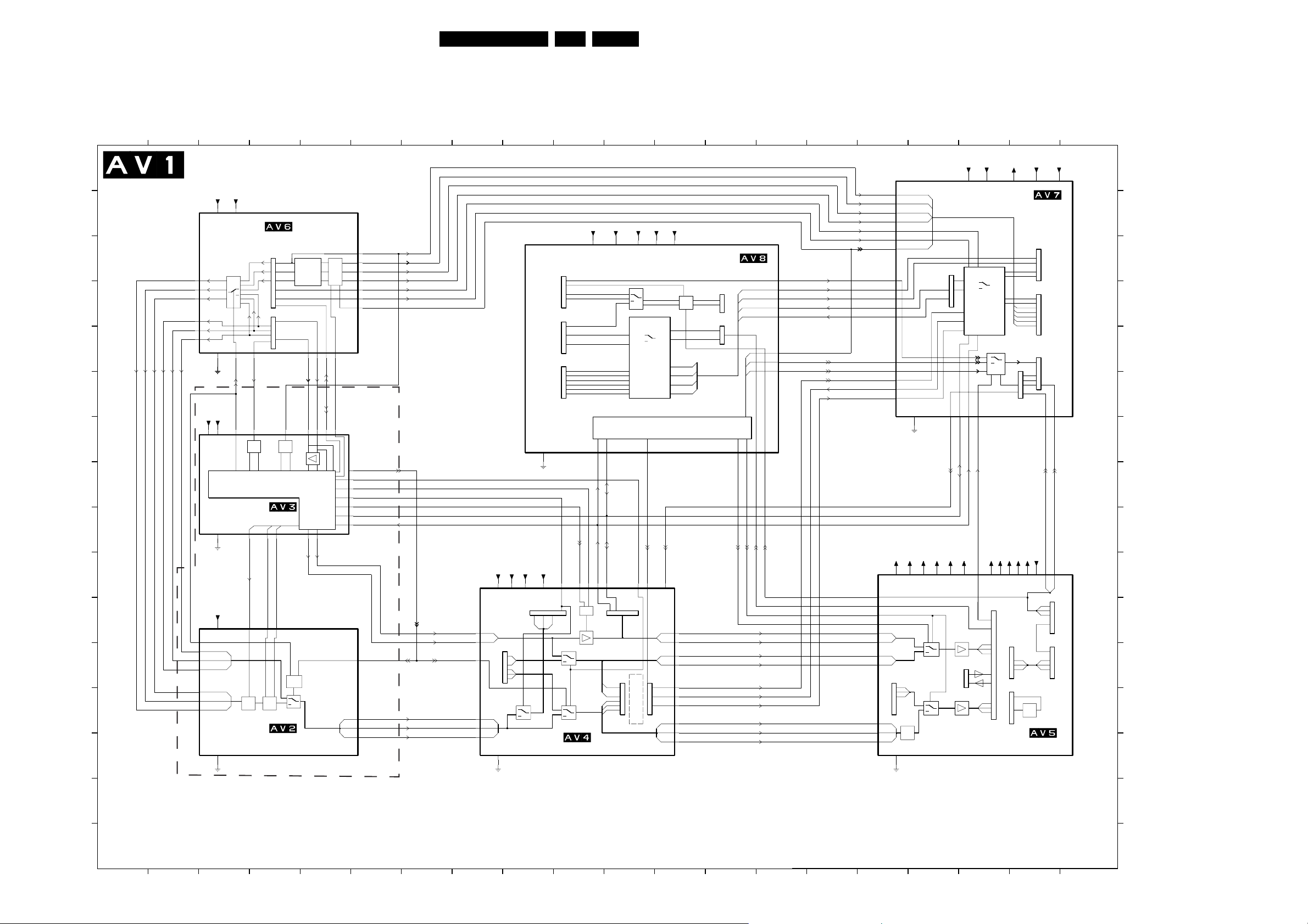
Circuit Diagrams and PWB Layouts
7. Circuit Diagrams and PWB Layouts
AV Interface Panel
44F21RE AB 7.
21
A
B
C
Pb_HD
Pr_HD
Y_HD
D
R_Pr_HD
G_Y_HD
B_Pb_HD
E
F
G
H
I
Y_HD
Pr_HD
Pb_HD
R_Pr_HD
G_Y_HD
B_Pb_HD
J
K
B_Pb_HD
L
M
G_Y_HD
R_Pr_HD
Y_HD
Pr_HD
Pb_HD
N
3
AV INTERFACE PANEL
DIAGRAM CONNECTIONS
+8VV
+8V6
+8V6+8VV
DIAGRAM
YPBPR-MATRIX
7670
GND
+5V
+5VSTB
+5V
+5VSTB
DIAGRAM
HD-SYNC-PROCESSING
GND
HD2_SEL
+8VV
+8VV
HD2_SEL
HD2_SEL
HD2_SEL
Y_HD2
Y_HD2
LM
1881
MATRIX_SELECT
MATRIX_SELECT
HD
matrix
7215
DIAGRAM
HD-MATRIX
GND
AV304
1
11
AV300
1
11
7351
HD_BLANKN
HD_BLANKN
HD_BLANKN
SYNC
rem.
7260
Y_HD1
PB_SD
PR_SD
Y_HD1
LM
1881
7360
HD_CLAMPN
HD_CLAMPN
HD_CLAMPN
MATRIX
7607
V_HD_EXT
V_HD_EXT
7375
V_HD V_HD_EXT
7280
H_HD_EXT
H_HD_EXT
H_HD_EXT
16:9_EXT3
H_HD
7610
1FH
16:9_EXT3
1FH
16:9_EXT3
1FH
Y_HD1
R_SD
G_SD
B_SD
USA ONLY
EXT_SYNC_PRESENT
VGA_SELECT
SYNC_TRISTATE
FBL_HD
NOT_SUPPORTED
SDA_S
SCL_S
H_HD
V_HD
Y_HD1
R_SD
G_SD
B_SD
CVBS_Y_EXT3
C_EXT3
FBL_YUV
EXT_SYNC_PRESENT
R_HD
G_HD
B_HD
VGA_SELECT
SYNC_TRISTATE
FBL_HD
EXT_SYNC_PRESENT
H_HD
V_HD
R_HD
G_HD
B_HD
Y_HD1
R_SD
G_SD
B_SD
CVBS_Y_EXT3
C_EXT3
FBL_YUV
AV328
1
11
AV302
1
6
AV305
1
11
GND
+5VSTBA
+8VV
+5V2
+5VSTBD
+8VV
+5VSTBA +5VSTBD
+5V2
FBL_HD
AV370
1
5
AV301
1
16
7400
7450
7420
DIAGRAM
VGA/HD-SELECTION
GND
+8VS
SCL_S
SCL_S
SYNC_TRISTATE
NOT_SUPPORTED
OR
7460
+5VSTBA
+5VSTBA
SDA_S
SDA_S
1
AV398
1
11
+5VSTBY
+5VSTBY
7840
TEA6422D
AUDIO
SELECTOR
VGA_SELECT
AV371
7
SCALER
+7V7
+7V7+8VS -7V7
7810
RESET_SCALER
RESET_SCALER
AV399
1
11
121110
-7V7
DIAGRAM
AUDIO+CONTROL
AV313
MUTE
7880
8574AT
I2C_SCALER_ACTIVE
HD
VD
H_HD_VGA
V_HD_VGA
CVBS_SCALER
Y_SCALER
C_SCALER
R_HD_VGA
G_HD_VGA
B_HD_VGA
1
6
AV373
1
7
PCF
POWER_VALID
CONFIG_IDENT
HD_VGA_SELECT
SYNC_TRISTATE_MON
RC_EXT
SNDL_MAIN_OUT
SNDR_MAIN_OUT
SNDR_FRONT
SNDL_FRONT
FBL_YUV
RC_FRONT_SEL_N
RC_FRONT_MON_SEL
15141398
POWER_VALID
CONFIG_IDENT
HD_VGA_SELECT
SYNC_TRISTATE_MON
167654
Y_HD1
CVBS_Y_EXT3
C_EXT3
FBL_YUV
RC_EXT
SNDL_MAIN_OUT
SNDR_MAIN_OUT
SNDR_FRONT
SNDL_FRONT
RC_FRONT_SEL_N
RC_FRONT_MON_SEL
CVBS_SCALER
Y_SCALER
C_SCALER
HD
VD
H_HD_VGA
V_HD_VGA
R_HD_VGA
G_HD_VGA
B_HD_VGA
R_SD
G_SD
B_SD
+8VV
AV340
1
9
+8VV
17
+8VVA
+8V6
+5VSTB
+5VSTB +5VSTBA +5VSTBY+8V6+8VVA
+5VSTBA
+5VSTBY
201918
A
DIAGRAM
VIDEO+RC-SELECTION
AV333
1
AV309
1
VIDEO
11
SELECTOR
7710
7740
GND
SCL_S
SDA_S
RC_MON
I2C_SCALER_ACTIVE
+8VS
+8VS
+7V7
-7V7
+8V6
+5V
-7V7
+8V6
+7V7
+5V2
RC_MON
+5V
+5V2
AV303
1
7575
7570
AV355
1
3
7550
7520
LPF
GND
OUTPUT-SELECTION+SUPPLY
16
DIAGRAM
+8VVA
+8VVA
AV307
1
11
AV315
1
9
AV341
1
9
+5VSTBA
+5VSTBD
+5VSTBD
+5VSTBA
11
AV372
1
9
AV308
1
11
+5VSTBY
+5VSTBY
HFB
GEN
50HZ_60HZ
+5VSTB
50HZ_60HZ
+5VSTB
AV306
AV310
POWER_ON
POWER_ON
1
9
1
9
B
C
D
E
F
G
H
I
J
K
L
M
N
O
P
3122 123 60092
123
45678
9 101112
13 14 15
16
17
CL 26532118_001.eps
18 19 20
O
P
221002
Page 45
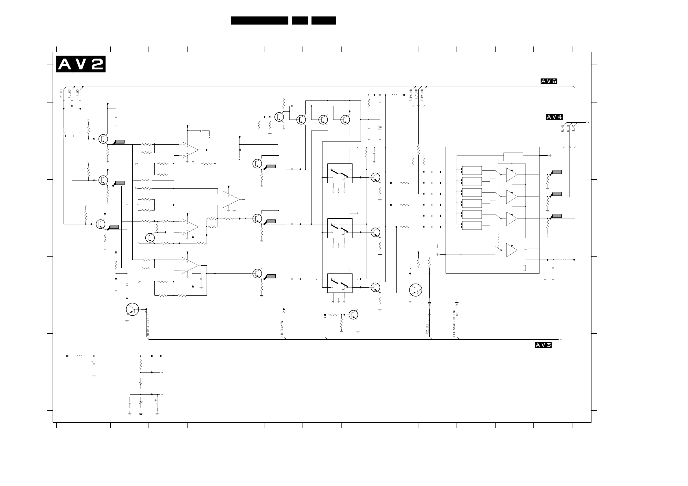
Circuit Diagrams and PWB Layouts
HD Matrix + Sync Remover Panel (USA only)
1 2345678 10111213
HD-MATRIX+SYNC REMOVER (USA ONLY)
AV6
AV6
A
B
C
D
E
F
G
H
I
AV6
I213
I212
I214
22u
22u
22u
2210
2205
2201
4V9
(0V)
3211
3202
4V9
(0V)
3206
4V9
(0V)
VREF1
I211
VREF1
22K
NTSC / ATSC
SELECTION
+8VV
3122 123 60092
5250
600R
1 2345
VREF1
22K
I202
22K
I206
BC847B
7211
2250
BC847B
7202
BC847B
7206
100u
+8A
3203
+8A
3207
+8A
3212
2251
F215
4V2
(0V)
560R
F216
PB
4V2
(0V)
560R
F217
4V2
(0V)
560R
+8A
10K
3231
2227
7246
PDTC124EU
100n
100n
I215
3215
1%
Y
1K8
3216
PR
1K2
1%
VREF2
3223
1%
Y
1K
3224
1%
1K
VREF2
3228
10K
PR
3229
560R
1%
I225
3230
1%
PB
1K
0V0
(0V)
VREF2
Y
1%
PB
1%
7230
BC847B
3237
2K2
3238
1K2
3241
4V6
I237
PR
1%
VREF2
I245
F246
3V3
(0V)
AV3
F250
3250
470R
F251
5V4
(0V)
6250
BAS316
F253
(0V)
4V7
2253
6251
100n
2252
BZM55-C4V7
4V3
(0V)
3217
1%
1K2
3219
22K
I228
3227
100R
1%
I231
470R
4V3
1%
3226
5K6
3239
1K2
3236
22K
HD-MATRIX
+8A
VREF1
VREF2
100u
+8A
2215
100n
7215-A
3
4
TSH95
I255
1
+8A
+8A
1%
13
4
13
4
13
7215-C
TSH95
+8A
7215-D
TSH95
+8A
8
9
9
3V7
(0V)
3218
1%
1K8
1% 1%
10
4V4
(0V)
3225
1%
330R
16
3V6
(0V)
2216
100n
3242
3243
22K
I229
1K
4V5
(0V)
4V5
(0V)
I259
8V4
5
6
3232
4V3
(0V)
(0V)
4V4
(0V)
4V3
(0V)
4V3
(0V)
4V4
2
12
11
I230
14
15
3240
2K2
FOR DC MEASSUREMENTS:
45F21RE AB 7.
I273
1K
F276
AV3
2255
220n
2257
220n
2259
220n
7273
BC847B
I260
I261
I262
2V7
(0V)
2V7
(0V)
2V7
(0V)
0V3
(0V)
7274
BC847B
7260-B
74HC4053D
Y0
2
Y1
1
Vss
8
7260-C
74HC4053D
Y0
5
Y1
3
7260-A
74HC4053D
Y0
12
Y1 Z
13
F277
3271
10K
HD_BLANKN
AV3
7275
BC847B
E
Vee
7
6
E
Vee8Vss
6
7
E
Vee8Vss
6
7
I271
3270
0V6
10K
16
16
16
(0V)
Vdd
Vdd
Vdd
I275
S
10
Z
15
S
9
Z
4
S
11
14
+8A
3273
7272
PMBT2369
0V7
I272
(0V)
10K
10K
3275
3272
+8A
2256
100n
7255
BC847B
7215-B
4
TSH95
7
4V6
8
(0V)
13
1K
I256
7257
BC847B
7259
BC847B
3255
3257
3259
3V0
(0V)
1K
3V9
(0V)
1K
2V9
(0V)
1K
HD_CLAMPN
F218
F227
F240
SYNC_REMOVER
CONNECT 480p YPbPr SIGNAL TO HD2 INPUT AND SELECT HD2 INPUT
6 7 8 9 10 11 12 13
I274
1K
3274
2274
2V5
(0V)
2u2
6275
2275
10K
3260
2260
100n
7265
BC847B
I265
2V7
(0V)
3265
7267
BC847B
I267
2V7
(0V)
3267
I263
7269
BC847B
I269
2V7 2V1
(0V)
(0V)
1V4
7271
PMBT2369
3269
100n
BZM55-C2V7
2V1
(0V)
1K
2V1
(0V)
1K
(0V)
1K
5274
F283
F288
F293
9
+8VV
100R
100R
100R
3282
3284
3286
AV6
AV6
3283
100R
3281
3285
100R
I281
I284
I286
I289
I291
I294
+8VV
10K
3296
F296
7296
PDTC124EU
FROM YPBPR-YUV-MATRIX
AV6
TO INPUT
7280
TDA8601T
16
IOCNTR
VIDOa
VIDOb
VIDOc
12
3287
11
3288
10
3289
13
FBO
0V
I280
1
Vp
9
GND
100R
3297
2281
2u2
2282
2u2
2283
2u2
2284
2u2
2285
2u2
2286
2u2
I297
10K
(0V)
5V3
(0V)
1V3
(0V)
1V3
(0V)
1V3
(0V)
1V3
(0V)
1V3
(0V)
1V3
I282
I285
I287
I290
I292
I295
DECODING
VIDIa1
VIDIa2
VIDIb1
VIDIb2
VIDIc1
VIDIc2
SEL
FBI1
FBI2
SELECTABLE
CLAMP
SELECTABLE
CLAMP
SELECTABLE
CLAMP
SELECTABLE
CLAMP
SELECTABLE
CLAMP
SELECTABLE
CLAMP
3-STATE
3-STATE
3-STATE
3-STATE
2
6
3
7
4
8
5
15
14
RGB / YPBPR SELECTION
0V3
(0V)
6297
BAT254
I298
AV3,6
6296
BAT254
AV3,4
FROM / TO HD-SYNC_PROCESSING
AV4
AV4
AV4
F268
1V3
(0V)
1K
F269
1V3
(0V)
1K
F270
1V3
(0V)
1K
(0V)
5280
8V4
2280
470n
CL 26532118_002.eps
600R
+8VV
221002
2201 B1
2205 B1
2210 B1
2215 B4
2216 F4
2227 F2
2250 H1
2251 B2
2252 I2
2253 I3
2255 C6
2256 C5
A
2257 E6
2259 F6
2260 C8
2274 B8
2275 B8
2280 F13
2281 C10
2282 D10
2283 D10
2284 D10
2285 D10
2286 E10
B
3202 B1
3203 C1
3206 C1
3207 D1
3211 D1
3212 E1
3215 C2
3216 C2
3217 C3
3218 C4
3219 C3
3223 C2
C
3224 D2
3225 E4
3226 E3
3227 E3
3228 D2
3229 D2
3230 E2
3231 F2
3232 D5
3236 F3
3237 F2
D
3238 F2
3239 F3
3240 F3
3241 E3
3242 D4
3243 E4
3250 H2
3255 C5
3257 E5
3259 F5
3260 C8
3265 D8
E
3267 E8
3269 G8
3270 G7
3271 G7
3272 B5
3273 B6
3274 B8
3275 B6
3281 C10
3282 D9
3283 C9
3284 D9
F
3285 C9
3286 E9
3287 D13
3288 D13
3289 E13
3296 F9
3297 F10
5250 H1
5274 A9
5280 F13
6250 I2
G
6251 I2
6275 B8
6296 G10
6297 G10
7202 B1
7206 C1
7211 E1
7215-A C4
7215-B D5
7215-C E4
7215-D F4
7230 E2
H
7246 G2
7255 C5
7257 D5
7259 F5
7260-A F7
7260-B C7
7260-C D7
7265 C8
7267 E8
7269 F8
7271 G8
7272 B6
I
7273 B6
7274 B7
7275 B7
7280 B10
7296 F9
F215 C2
F216 D2
F217 E2
F218 C6
F227 E6
F240 F6
F246 G2
F250 H3
F251 H3
F253 I3
F268 C13
F269 D13
F270 D13
F276 G6
F277 G7
F283 C9
F288 D9
F293 E9
F296 F9
I202 C1
I206 D1
I211 E1
I212 B1
I213 B1
I214 B1
I215 B3
I225 D3
I228 D3
I229 E4
I230 E3
I231 E3
I237 E3
I245 G2
I255 C4
I256 D5
I259 F4
I260 C6
I261 E6
I262 F6
I263 F8
I265 C8
I267 E8
I269 F8
I271 G8
I272 B5
I273 B6
I274 A8
I275 B8
I280 E13
I281 C10
I282 C10
I284 C10
I285 D10
I286 D10
I287 D10
I289 D10
I290 D10
I291 D10
I292 E10
I294 E10
I295 E10
I297 F10
I298 G10
Page 46
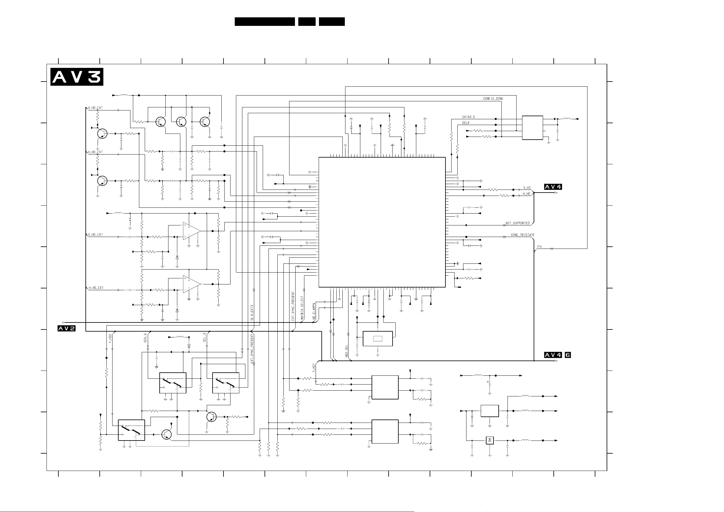
Circuit Diagrams and PWB Layouts
Sync Processing Panel (USA only)
46F21RE AB 7.
A
B
C
D
E
F
FROM HD-
G
H
I
MATRIX
3122 123 60092
12
34
567
SYNC-PROCESSING (USA ONLY)
5303
600R
3302
10K
2u2
2302
3306
10K
2u2
2306
2321
2320
470n
I323
2330
470n
I332
74HCT4053D
Y0
Y1
Vee8Vss
7
6
100n
E
F302
3303
470K
I302
16
Vdd
3320
3321
3322
3330
3331
3332
(0V)
0V5
7302
BC847B
BC847B
0V
(0V)
2303
73047303
BC847B
100n
I309
2304
100n
F311
I307
3307
100R
3309
100R
I310
3308
3310
4K7
4K7
2307
2u2
2312
100n
2308
(0V)
0V
2314
47p
47p
3312
3314
3311
220K
470K
3313
220K
470K
F321
5V
(0V)
3324
4K7
3334
4K7
I333
I324
2322
2333
100n
10n
(0V)
(0V)
1V0
1V0
0V9
I325
(0V)
0V9
I334
6322
6334
100K
I322
2K2
22K
100K
2K2
22K
3323
100K
I331
3333
100K
+5VSTB
AV4,7,8
I343
5V1
(5V1)
2340
100n
7340-C
74HCT4053D
Y0
5
4V5
(4V5)
Y1
3
Vee7Vss
E
8
6
3347
47K
+5A
7341
S
10
BC847B
I341
Z
15
2V6
(0V)
2V0
(0V)
5340
9
10
BAS316
4
5
BAS316
16
Vdd
F341
11
6
11
GND
6
I340
6340
SDA_EPLD
S
9
4
Z
4V5
(4V5)
(5V0)
0V
7321-B
LM319D
GND
8
7321-A
LM319D
3
BAT254
0V
(0V)
I347
BC847B
(0V)
I346
3346
7347
0V3
7
12
0V3
(0V)
4V5
10K
2311
100n
2313
10n
F326
F336
AV4,7,8
74HCT4053D
Y0
12
Y1
13
3316
3325
3326
3335
3336
7340-A
Vss
8
0V7
(0V)
F312
F313
F314
470K
F306
1K
2K2
1K
2K2
Vee
7
I349
3349
7360
EP1K10TC144-3
1
AV2
2K2
(0V)
(0V)
3378
1K
3380
1K
AV2
2
3
4
5
6
7
8
9
10
11
12
13
14
15
16
17
18
19
20
21
22
23
24
25
26
27
28
29
30
31
32
33
34
35
36
AV2
TCK
CONF-DONE
CEO_
TDO
VCCIO1
GNDINT1
CLKUSR
IO1
IO2
IO3
RDY_BUSY
IO4
IO5
INIT-DONE
GNDINT2
VCCINT1
IO6
IO7
IO8
IO9
IO10
IO11
IO12
VCCIO2
GNDINT3
IO13
IO14
IO15
IO16
IO17
IO18
IO19
IO20
TMS
STATUS_
IO21
HD_BLANKN
AV6,7
2360
CONFIG_DONE
100n
3V3
V_SYNC_TTL
V_SYNC_POLN
2V5
3V3
H_C_SYNC_TTL
H_C_SYNC_POLN
75OHM_ON
2361
100n
2362
100n
F309
V_SYNC_COMP
H_SYNC_COMP
C_SYNC_OUT
LM_CSYNC_2
0V
0V
LM_VSYNC_2
LM_VSYNC_1
LM_CSYNC_1
2V5
AV6
3379
2K2
AV2,4
F378
F379
3381
AV2,4
16
Vdd
S
11
Z
14
4V5
E
(4V5)
6
3348
10K
22K
+5A
3345
I350
1K
2K2
2K2
3356
3354
3350
100R
F353
I354
F355
CONNECT 480p YPbPr SIGNAL TO HD2 INPUT AND SELECT HD2 INPUT
+5V
75R
3301
7301
I301
BC847B
I311
I304
0V
(0V)
75R
3305
I305
7305
I308
BC847B
I306
0V
(0V)
5321
+5V
600R
AV6
F343
2K2
3343
I342
+5A
3342
3344
7340-B
2
1K
2V6
(0V)
1
2V5
(0V)
1K
FOR DC MEASSUREMENTS:
123456
910
SDA_EPLD
I361
I362
3V3
RES
RES
100R
I357
3358
100R
2371
100n
I363
16:9_EXT3
2373
100n
3V3
8
SCL_EPLD
2V5
3357
100n
2372
I358
140
139
142
141
143
144
CS
RS_
CS_
WS_
IO79
IO78
GNDINT13
IO75
IO76
IO77
134
VCCIO8
129
128
IO71
IO72
IO73
IO74
DEV-OE
VCCINT6
GNDINT12
130
131
132
133
135
136
137
138
123
127
125
124
126
GNDINT11
DEDICATED-INP3
DEDICATED-INP4
DEDICATED-CLK-PINS
121
122
IO70
DEV-CLR_
117
115
110
111
112
113
114
116
118
119
120
IO66
IO67
IO68
IO69
DATA7
VCCIO7
DATA6
DATA5
DATA4
DATA3
DATA2
DATA1
GNDINT10
EPLD
SYNC PROCESSING +
FORMAT DETECTION
IO2439IO2541IO2643IO2744IO29
I366
3377
100R
3353
1K
3355
1K
IO2237IO23
38
F367
FBL_HD
VGA_SELECT
AV4
I378
AV4
GNDINT4
40
2377
100n
2353
100n
LOCK
42
I376
I377
I379
I355
I353
I356
VCCIO3
I028
45
2363
3V3
3V3OSC
2380
AV2,6
0V
1V4
0V
3V5
1V9
3V6
46
IO3048IO3149IO32
47
2364
100n
2V5
7380
FXO-31FL
1
TS
100n
(0V)
(0V)
(0V)
(0V)
(0V)
(0V)
VCC-CKLK
VCCINT2
GNDINT552GNDINT6
DEDICATED-INP154DEDICATED-INP2
53
50
51
100n
3V3
(0V)
F380
4
VDD
OSC
GND
2
7375
LM1881M
1
CSYNC
2
VIN
3
VSYNC
4
GND
7351
LM1881M
1
CSYNC
2
VIN
3
VSYNC
4
GND
SYNC SEPARATOR
789
GCLK155GND-CKLK
57
58
56
F381
3
OUT
VS
O|E-FI
RSET
BG|BP
VS
O|E-FI
RSET
BG|BP
VCCIO4
IO3359IO3460IO35
61
2365
5V0
(0V)
8
7
6
1V2
(0V)
5
5V0
(0V)
8
7
6
1V2
(0V)
5
IO3663IO3764IO3865IO39
62
100n
3V3
+5A
I375
+5A
I352
IO4068IO4169IO4270IO43
GNDINT7
67
66
2366
2375
100n
2376
100n
3376
220K
2351
100n
2352
100n
3352
220K
100n
VCCIO5
71
3V3
11 12 13
109
DATA0
DCLK
VCCINT5
IO65
IO64
IO63
IO62
IO61
IO60
IO59
IO58
VCCIO6
GNDINT9
IO57
IO56
IO55
IO54
IO53
IO52
IO51
VCCINT4
GNDINT8
IO50
IO49
IO48
IO47
IO46
IO45
MSEL0
MSEL1
VCCINT3
CONFIG_
IO44
72
7385
(0V)
(0V)
(0V)
(0V)
F370
F371
EPC1441
1
DATA
2
DCLK
3
OE
4
CS_
PROM
AV6
F383
0V
F384
3386
3V3
3V3
3359
100R
3360
100R
I359
I360
108
107
106
CE_
105
TDI
104
103
102
101
I373
0V1
100
99
98
97
96
95
94
93
92
91
I364
0V
90
89
(0V)
88
87
F365
86
85
84
83
82
81
80
79
78
77
76
75
74
73
I315
1315
2370
100n
0V1
2369
100n
2368
100n
2367
100n
3315
1K
3387
1K
2V5
I374
3V3
2V5
2V5
3V3
0V
F386
3V3
F387
3V3
1K
3373
100R
3374
100R
1
(0V)
3V3
8
VCC1
7
VCC2
6
CASC_
5
GND
TO INPUT
AV4
AV4
AV4
AV4
FROM / TO
5350
+5V
+5V
2390
2393
10 11 12 13
600R
7390
LD1117
3
100n
LD1117DT25
100n
2350
IN
GND
7393
3IN2
GND
F350
+5A
100u
F392
5390
600R
5391
F391
2
OUT
1
OUT
1
2391
2394
100n
F394
100n
600R
5392
600R
3V3
(0V)
F393
3V3
(0V)
F395
2V5
(0V)
5385
600R
I385
2385
100n
3V3OSC
3V3
2V5
CL 26532118_003.eps
3V3
221002
1315 E10
2302 B2
2303 B4
2304 B4
2306 C2
2307 B3
2308 B3
2311 B4
2312 C3
2313 C4
2314 C3
2320 D2
2321 D2
2322 E3
A
2330 E2
2333 F3
2340 G3
2350 H11
2351 I9
2352 I9
2353 I8
2360 C6
2361 D6
2362 D6
2363 F8
B
2364 F8
2365 F9
2366 F9
2367 E10
2368 D11
2369 C10
2370 C11
2371 B9
2372 B8
2373 B8
2375 H9
2376 H9
C
2377 H8
2380 G8
2385 B12
2390 I10
2391 I11
2393 I10
2394 I11
3301 A1
3302 B2
3303 A2
3305 B1
3306 C2
D
3307 B3
3308 B3
3309 C3
3310 C3
3311 B4
3312 B4
3313 C4
3314 C4
3315 E10
3316 C4
3320 D2
E
3321 D2
3322 E2
3323 E3
3324 D3
3325 D4
3326 D4
3330 E2
3331 F2
3332 F2
3333 F3
3334 E3
3335 E4
F
3336 F4
3342 I1
3343 H2
3344 I1
3345 I5
3346 H4
3347 H3
3348 I5
3349 I5
3350 I7
3352 I9
3353 I7
G
3354 I6
3355 I7
3356 I6
3357 B8
3358 B9
3359 B10
3360 B10
3373 C11
3374 C11
3376 H9
3377 H7
H
3378 H7
3379 H6
3380 H7
3381 H6
3386 B11
3387 B11
5303 A2
5321 D2
5340 G3
5350 H11
5385 A13
5390 H12
I
5391 H12
5392 I12
6322 E3
6334 F3
6340 G4
7301 B2
7302 A3
7303 A3
7304 A4
7305 C2
7321-A E4
7321-B D4
7340-A G4
7340-B I2
7340-C G3
7341 I3
7347 I4
7351 I8
7360 B7
7375 H8
7380 F8
7385 A12
7390 H11
7393 I11
F302 A2
F306 C5
F309 D6
F311 B5
F312 B5
F313 C5
F314 C5
F321 D4
F326 D4
F336 E4
F341 I4
F343 G2
F350 H11
F353 I7
F355 I7
F365 D10
F367 F7
F370 C12
F371 C12
F378 H6
F379 H6
F380 F8
F381 F9
F383 A11
F384 A11
F386 B11
F387 B11
F391 H12
F392 H12
F393 H12
F394 I12
F395 I12
I301 B1
I302 B2
I304 B1
I305 C1
I306 C2
I307 B3
I308 C1
I309 A4
I310 C3
I311 B2
I315 E10
I322 D3
I323 E2
I324 E3
I325 D3
I331 E3
I332 F2
I333 F3
I334 E3
I340 G4
I341 I3
I342 H2
I343 G3
I346 G4
I347 H4
I349 I5
I350 I6
I352 I9
I353 I8
I354 I7
I355 I8
I356 I8
I357 B9
I358 B9
I359 B10
I360 C10
I361 A9
I362 A9
I363 A7
I364 D10
I366 F7
I373 C10
I374 C11
I375 H9
I376 H8
I377 H8
I378 H7
I379 H8
I385 A12
Page 47
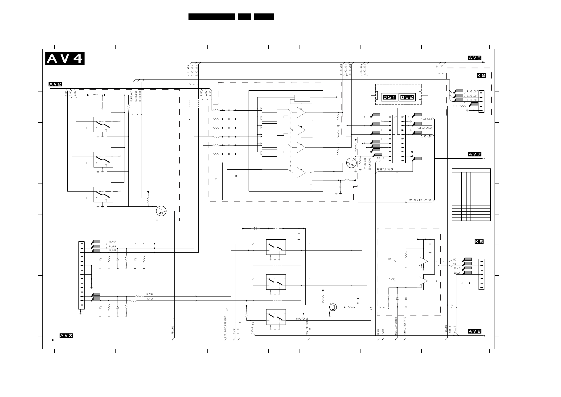
Circuit Diagrams and PWB Layouts
VGA / HD Selection Panel
47F21RE AB 7.
123456
A
FROM HD-MATRIX
AV2
AV2
B
C
D
E
F
G
VGA INPUT
CONNECTOR
15P
MINI
"D" SHELL
H
I
FROM SYNC PROCESSING
3122 123 60092
123456789101112
VGA/HD-SELECTION
AV2
I400
5400
+8VV
600R
100n
2400
10K
3400
8V4
(0V)
16
Vdd
S
11
Z
14
0V
(0V)
E
6
16
Vdd
S
10
15
0V
(0V)
E
6
16
Vdd
S
9
Z
4
0V
(0V)
E
6
HD-TRISTATE
75R
3442
BZM55-C33
3445
BZM55-C33
3441
6441
BZM55-C33
1K
3444
6444
BZM55-C33
75R
1K
3447
100R
6440
8V3
(0V)
3440
BZM55-C33
3446
100R
3419
75R
+8VV
F419
10K
I440
I441
I442
AV301
0301
1
2
3
4
5
6
7
8
9
10
11
12
13
14
15
16 17
1V2
(0V)
1V2
(0V)
1V2
(0V)
NC.
NC.
NC.
NC.
NC.
NC.
F443
7400-A
74HC4053D
Y0
12
Y1
13
Vee7Vss
8
7400-B
74HC4053D
Y0
2
Y1 Z
1
Vee8Vss
7
7400-C
74HC4053D
Y0
5
Y1
3
Vss
Vee
7
8
F440
F441
F442
6442
I443
F444
F445
6445
USA ONLY
7419
PDTC124EU
0V
(0V)
AV3
7 8 9 10111213 14
TO OUTPUT+SUPPLY
AV5
AV7
AV7
AV7
AV7
2460
0V4
(0V)
0V7
(0V)
100n
AV5
USA ONLY
F410
F411
F412
FBL_HD
3410
1K
TO VIDEO
[AV4] VGA/HD-SELECTION
Item
4408 X Jumper
4410 X Jumper
4412 X Jumper
4450 X Jumper
4451 X Jumper
7450-B X PC74HCT4538T
7450-A X PC74HCT4538T
FROM CONTROL
CL 26532118_004 .eps
AV3,7,8
AV3,7,8
AV3
+RC
EU + AP
USA
F460
F461
F462
F463
F464
TO 0370
SOURCE
SELECTION
AV370
0370
F409
F408
Description
FROM/TO
0371
SOURCE
SELECTION
AV371
0371
1
2
3
4
5
NC.
6
7
NC.
1
2
3
4
5
221002
AV5
AV5
AV5
AV5
I436
3432
3433
3434
I420
2420
AV5
SCALER PANEL
0398
AV398
0398
H_HD_VGA
F430
F431
F432
F433
F434
F439
F429
1
2
3
4
5
6
7
8
9
10
11
AV8
AV8
R_HD_VGA
1K
G_HD_VGA
B_HD_VGA
1K
+5V
RES
3435
1K
7435
RES
3437
+8VV
5420
600R
470n
AV399
0399
1
2
3
4
5
6
7
8
9
10
11
0399
F435
F436
F437
+5V2
+5V2
F438
AV5
AV5
AV5
I422
I424
I426
I428
I430
I432
1V2
(0V)
1V2
(0V)
1V2
(0V)
1V2
(0V)
1V2
(0V)
1V2
(0V)
(0V)
(0V)
5V1
(0V)
0V
0V
7420
TDA8601T
2
VIDIa1
6
VIDIa2
3
VIDIb1
7
VIDIb2
4
VIDIc1
8
VIDIc2
5
SEL
15
FBI1
14
FBI2
SELECTABLE
CLAMP
SELECTABLE
CLAMP
SELECTABLE
CLAMP
SELECTABLE
CLAMP
SELECTABLE
CLAMP
SELECTABLE
CLAMP
DECODING
3-STATE
3-STATE
3-STATE
3-STATE
IOCNTR
VIDOa
VIDOb
VIDOc
16
12
1V2
(0V)
11
1V2
(0V)
10
1V2
(0V)
13
FBO
1V2
(0V)
1
Vp
8V4
(0V)
9
GND
AV2
3421
100R
3423
100R
3425
100R
3427
100R
3429
100R
3431
100R
2451
USA ONLY
I421
2421
2u2
I423
2423
2u2
I425
2425
2u2
I427
2427
2u2
I429
2429
2u2
I431
2431
2u2
22n
+5V
AV2
AV2
*
4408
*
*
4412
4410
HD-VGA SELECTION
AV2,3
+5VSTBA
AV3
AV3
(5V1)
I451
3452
5V2
I452
6450
BAT254
+5VSTBA
10K
I454
0V
(0V)
0V
(0V)
0V
(0V)
0V
(0V)
4V7
(4V7)
5V2
(5V1)
AV3,7,8
I449
5V1
(4V9)
7450-B
74HCT4053D
Y0
2
Y1 Z
1
7450-A
74HCT4053D
Y0
12
Y1
13
7450-C
74HCT4053D
Y0
5
Y1
3
5450
(4V9)
600R
*
16
Vdd
S
10
15
Vee8Vss
E
6
7
4450
*
*
16
Vdd
S
11
Z
14
E
Vee7Vss
8
6
4451
*
16
Vdd
S
9
Z
4
Vee8Vss
E
6
7
5V1
0V
(0V)
0V
(0V)
0V
(0V)
4V7
(4V7)
2450
I450
I455
100n
AV3
3453
+5VSTBA
7453
10K
BC847B
0V6
(0V)
I456
3456
10K
I453
USA ONLY
F465
47K
3461
6462
AV3
AV3
AV3
3V3
BAS316
(0V)
+5VSTBD
3462
6463
3V3
(0V)
AV3
7460-A
74HCT125D
RES
2
0V
(0V)
2V8
(0V)
7460-B
74HCT125D
5
0V
(0V)
4
BUFFER
BAS316
I460
4V9
14
3
7
1
14
6
7
0301 F1
0370 A14
0371 G14
0398 B11
0399 B12
2400 B2
2420 E10
2421 B6
2423 B6
2425 C6
2427 C6
2429 C6
2431 C6
2450 F8
A
2451 D6
2460 F13
3400 B3
3410 B14
3419 E4
3421 B6
3423 B6
3425 C6
3427 C6
3429 C6
3431 C6
3432 B10
3433 C10
B
3434 C10
3435 C10
3437 D10
3440 G3
3441 G3
3442 G2
3444 I3
3445 I2
3446 H3
3447 H3
3452 I7
3453 H9
3456 H10
C
3461 H11
3462 G12
4408 B5
4410 B5
4412 B5
4450 G8
4451 H8
5400 B2
5420 D10
5450 F8
6440 G3
6441 G2
D
6442 G2
6444 I2
6445 I2
6450 F7
6462 H12
6463 H12
7400-A B2
7400-B C2
7400-C D2
7419 E4
7420 A7
7435 D10
7450-A G8
E
7450-B F8
7450-C H8
7453 H10
7460-A G12
7460-B G12
F408 B14
F409 B14
F410 A14
F411 B14
F412 B14
F419 E4
F429 D11
F430 B11
F
F431 C11
F432 C11
F433 C11
F434 C11
F435 B12
F436 C12
F437 C12
F438 D12
F439 C11
F440 F2
F441 G2
F442 G2
G
F443 G2
F444 H2
F445 H2
F460 G14
F461 G14
F462 G14
F463 G14
F464 H14
F465 H12
I400 B2
I420 D10
I421 B6
I422 B6
H
I423 B6
I424 B6
I425 C6
I426 C6
I427 C6
I428 C6
I429 C6
I430 C6
I431 C6
I432 D6
I436 D10
I440 F4
I441 G4
I
I442 G4
I443 H2
I449 F7
I450 F9
I451 H7
I452 G7
I453 H11
I454 I7
I455 I9
I456 H10
13 14
Page 48
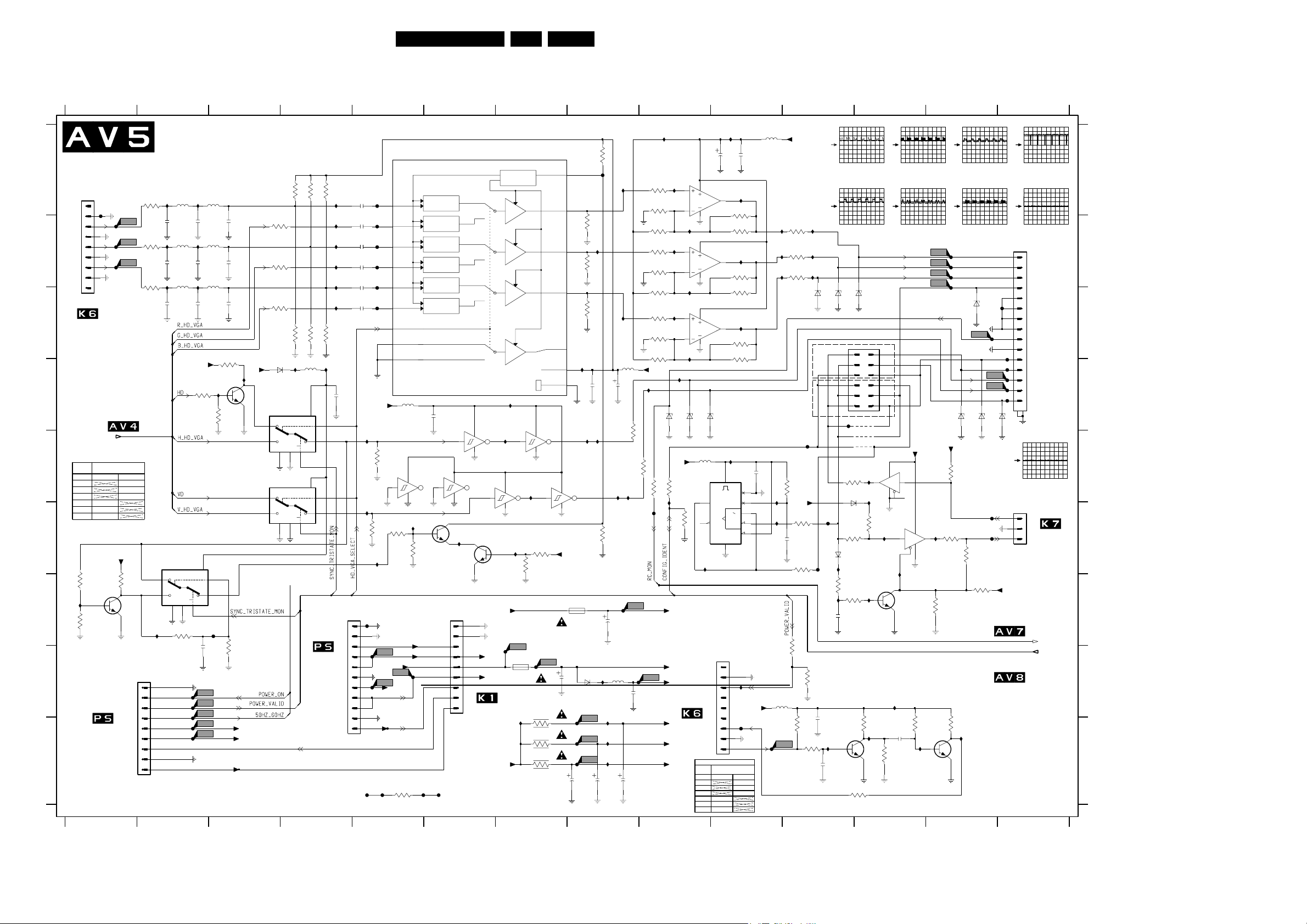
Circuit Diagrams and PWB Layouts
Output Selection + Supply Panel
48F21RE AB 7.
1
A
AV340
0340
1
F520
2
3
4
B
5
6
7
8
9
FROM 340
C
VIDEO
CONTROL
D
FROM INPUT
E
F
G
H
CON.
1519
1 2
3 4
5 6
7 8
9 10
11 12
3541
I542
3543
I
3122 123 60092
FTV 1.9
10K
7540
PMBT2369
0V6
(0V)
10K
FROM 0306
SUPPLY
1234567
NC.
R_VC
G_VC
B_VC
NC.
JUMPERS
F521
F525
F529
FTV 2.3
+5VSTBA
3540
2345678
OUTPUT-SELECTION
+SUPPLY
3523
100R
3527
100R
3531
100R
6570
BAT254
7570-A
74HCT4053D
Y0
12
Y1
13
7570-C
74HCT4053D
Y0
5
Y1
3
STANDBY
3536
3522
I580
Vee8Vss
7
Vee8Vss
7
AV7
AV7
4K7
1
2
3
4
5
6
7
8
9
AV306
0306
3521
470R
3525
470R
3529
470R
2V7
(0V)
0V5
(5V1)
I541
5V2
(5V2)
0V
(0V)
-6V8
(-0V2)
0V
(0V)
AV4
AV4
AV4
AV4
AV4
AV4
AV4
2
1
5523
I535 I536
3u9
39p
2522
5529
I537
3u9
39p
2528
5535
I539
3u9
39p
2534
+5VSTBA
7570-B
74HCT4053D
Y0
Y1
E
Vee7Vss
6
8
3542
100K
4V8
(0V2)
7V6
(0V2)
0V5
(3V2)
I538
I540
2524
2530
2536
16
Vdd
3573
10K
2542
F501
F503
F504
F505
56p
56p
56p
S
Z
F502
5525
3u3
5531
3u3
5537
3u3
PMBT2369
I573
0V3 (0V)
3575
0V3
10
(3V5)
2V6
15
(0V)
0V
(5V1)
F534
100n
3574
4K7
7573
2526
2532
2538
10K
3544
22p
22p
22p
220K
+16V
+5VSTBA
I574
(0V)
0V4
(0V)
0V
+7V7
-7V7
(0V)
0V
(5V1)
2V7
680R
3537
3526
470R
5570
600R
16
Vdd
E
6
16
Vdd
E
6
AV8
FROM 0307
AV8
680R
3538
3530
470R
I570
S
11
Z
14
S
9
Z
4
SUPPLY
(0V)
(0V)
0V4
4V9
0V
(0V)
(0V)
2V7
680R
I521
I523
I525
I527
I529
I531
470R
2570
0V
10
11
100n
AV8
1
2
3
4
5
6
7
8
9
AV307
0307
2521
2u2
2523
2u2
2525
2u2
2527
2u2
2529
2u2
2531
2u2
+5VSTBA
I571
I572
AV8
F596
F506
+33V
F522
F523
F524
F526
F528
F530
3572
(0V)
2V4
(0V)
2V1
(0V)
2V4
(0V)
2V1
(0V)
2V4
(0V)
2V1
3571
I544
2
6
3
7
4
8
5
15
14
47K
7575-E
74HCT14D
47K
F507
+5VSTB
F516
+5VSTBY
+33V
F597
7520
TDA8601T
VIDIa1
VIDIa2
VIDIb1
VIDIb2
VIDIc1
VIDIc2
SEL
FBI1
FBI2
5575
600R
14
11 10
7
I543
3547
10K
3548
5V2
(0V)
F509
(0V1)
F598
3599
1K
SELECTABLE
CLAMP
SELECTABLE
CLAMP
SELECTABLE
CLAMP
SELECTABLE
CLAMP
SELECTABLE
CLAMP
SELECTABLE
CLAMP
2575
7575-F
74HCT14D
13
(0V)
0V6
10K
+5V2_FB
5V2
+5V2
(0V)
+8V6
8V8
+33V
33V
+16V
F599
100n
7575-A
74HCT14D
(0V)
12
2V7
14
12
(0V)
7
0V4
7546
PMBT2369
(0V)
I581
0V
AV310
0310
1
2
3
4
5
+5VSTB
6
7
TO 0310
8
9
TUNER-IF
DECODING
3-STATE
3-STATE
3-STATE
3-STATE
I575
7575-B
74HCT14D
14
I576
0V4
7
(5V2)
BUFFER
7575-C
74HCT14D
14
56
7
7568
BC847B
+5V2
5V2
(5V2)
+8V6
+8V6
(0V6)
0V6
+5V2
I582
F508
1513
T200mA
250V
19372
I510
16
IOCNTR
(0V)
0V7
12
VIDOa
(0V)
2V3
11
VIDOb
(0V)
2V3
10
VIDOc
(0V)
2V3
13
FBO
1
Vp
9
GND
14
7
7575-D
3568
22K
3512
1R
3510
1R
3511
4R7
F514
(0V)
4V6
14
9
7
+5VSTBA
1512
T200mA
19372
2513
100u
2510
34
74HCT14D
I577
5V2
(5V2)
10K
3590
L
910111213
(0V)
8V6
8
250V
I520
H_CLAMP
3533
3534
3535
I578
(0V)
0V
L
6513
BAT254
F513
F510
F511
100u
F533
I534
2520
I592
2511
I552
8K2
3520
100R
3579
100n
I569
F515
3562
100R
3553
470R
3550
3563
100R
3554
470R
3551
3564
100R
3555
470R
3552
+8VV
100R
3580
1K
1K
1K
100R
F581
AV7
+5V
+8VVA
+8VV
+8VS
I562
(0V)
2V3
(0V)
2V3
I563
(0V)
2V3
(0V)
2V3
I564
(0V)
2V3
(0V)
2V3
I568
6580
BZM55-C33
+5VSTBD
1R
3591
I591
AV8
+5VSTBA
+5VSTBD
FROM 0315
CONTROL
5
6
I553
10
9
I554
12
13
I555
6578
74HCT4538
4K7
3592
VIDEO
*
I533
1K
1K
1K
I532
5520
600R
22u
2519
470n
3578
I579
I593
10K
3519
F512
2512
100u
I514
5513
600R
2515
I511
I512
I513
100u
100u
2514
I550
100u
2551
7550-A
4
TSH93
7
(0V)
1V8
11
7550-B
4
TSH93
8
(0V)
1V8
11
7550-C
4
TSH93
14
(0V)
1V8
11
6579
BZM55-C33
BZM55-C33
I545
5545
600R
7545-A
16
0V
6
4V7
RCX
1
7
8
I549
(0V)
(4V7)
ONESHOT
AV315
0315
9
8
7
6
5
4
3
2
1
EXPLANATION
CON.
JUMPERS
1519 FTV 1.9
1 2
3 4
5 6
7 8
9 10
11 12
CX
LINEDRIVE
2550
I556
3565
470R
3556
1K
I557
3566
470R
3557
1K
I558
3567
470R
3558
1K
4V7
(4V7)
>
R
NC.
I584
NC.
NC.
F584
FM 23
100n
1
2
4
5
3
+8VV
2545
4V7
(4V7)
HFB
0V
4V7
(4V7)
(0V8)
3V3
5550
600R
100n
I546
I547
5585
600R
I561
I566
I559
H_MON
F585
3545
2546
+8VV
3559
75R
3560
75R
3561
75R
V_MON
2.3
470K
+5VSTBA
3546
2u2
3539
3K3
3584
3585
1K
AV8
15K
F592
3594
10K
2V / div DC
20µs / div
F525
I565
I567
I560
3586
4K7
2V / div DC
20µs / div
6561
6560
6559
BZM55-C33
BZM55-C33
1519
1
34
1.9
56
78
9
11 12
F519
4519
4520
4521
3582
100R
6595
5V2
(5V2)
BAT254
F548
3583
100R
6571
BAT254
F518
I590
BUFFER
1K
3570
3576
I551
47K
100n
2571
33K
HFB GENERATOR
2585
100n
7587
BC847B
I586
0V6
(0V1)
470p
2587
3593
1K
BZM55-C33
74HCT125D
I599
I596
3595
4V9
(4V9)
I594
0V6
(0V6)
3587
I587
F521
7460-D
5V0
(5V0)
4V9
(4V9)
7571
BC847B
10K
2
10
14
11
7
74HCT125D
4K7
I597
1V3
(0V)
3581
7460-C
I585
270p
10K
F529
2V / div DC
20µs / div
F559
1V / div DC
20µs / div
5V0
(5V0)
12
13
9
10
I595
0V
(0V)
+5VSTBD
3V9
(3V9)
14
8
7
(4V9)
F560
F595
4V9
I598
3569
F559
F561
+5VSTBA
3596
3597
2K2
10K
F560
F561
6582
4K7
3598
1V / div DC
20µs / div
1V / div DC
20µs / div
6584
F580
BZM55-C33
3V9
(3V9)
3V0
(3V0)
3K3
TO VIDEO+RC
FROM/TO CONTROL
2588
3588
(0V1)
0V6
27K
PMBT2369
I588
7589
3589
I589
2K2
0V9
(0V1)
8 9 10 11 12 13 14
BZM55-C33
6581
F582
F583
3577
6K8
R_MON
G_MON
B_MON
F562
F576
F577
F578
F579
F591
6583
BZM55-C33
TXDO
RXDO
14
F578
2V / div DC
20µs / div
F579
2V / div DC
5ms / div
AV303
0303
1
2
3
4
5
6
MONITOR
7
OUTPUT
CONNECTOR
8
9
10
15P
MINI
11
"D" SHELL
12
13
14
15
17
16
BZM55-C33
F580
2V / div DC
20µs / div
AV355
0355
TO 0355
1
2
TXT &
3
CONTROL
+5VSTBA
CL 26532118_005.eps
221002
0303 B14
0306 H2
0307 G4
0310 G6
0315 H10
0340 A1
0355 F14
1512 G8
1513 H7
1519 C11
2510 I7
2511 I8
A
2512 G8
2513 H7
2514 I8
2515 H8
2519 D8
2520 D8
2521 A5
2522 B2
2523 B5
2524 B2
2525 B5
2526 B3
2527 B5
2528 B2
B
2529 B5
2530 B2
2531 C5
2532 B3
2534 C2
2536 C2
2538 C3
2542 H2
2545 E10
2546 F11
2550 A10
2551 A10
2570 D4
C
2571 G11
2575 D6
2585 I11
2587 I11
2588 I12
3510 I7
3511 I7
3512 I7
3519 F8
3520 A8
3521 A2
3522 C4
3523 B3
D
3525 B2
3526 C4
3527 B3
3529 B2
3530 C4
3531 C3
3533 B8
3534 B8
3535 C8
3536 A4
3537 A4
3538 A4
E
3539 F11
3540 G1
3541 G1
3542 G2
3543 G1
3544 H3
3545 E11
3546 F11
3547 F5
3548 F5
3550 B9
3551 C9
3552 C9
F
3553 A9
3554 B9
3555 C9
3556 B10
3557 C10
3558 C10
3559 B11
3560 B11
3561 B11
3562 A9
3563 B9
3564 C9
3565 A10
G
3566 B10
3567 C10
3568 F7
3569 G13
3570 G11
3571 E5
3572 F5
3573 D2
3574 D3
3575 D3
3576 G11
3577 G13
H
3578 E8
3579 E9
3580 E9
3581 I12
3582 E11
3583 F11
3584 H11
3585 I11
3586 I11
3587 I12
3588 I12
3589 I13
3590 F7
3591 E9
I
3592 F9
3593 I12
3594 H11
3595 F12
3596 E13
3597 F13
3598 F13
3599 I5
4519 D12
4520 E12
4521 E12
5513 H8
5520 D8
5523 A2
5525 A3
5529 B2
5531 B3
5535 B2
5537 B3
5545 E9
5550 A10
5570 D4
5575 D5
5585 H10
6513 H8
6559 C11
6560 C11
6561 C11
6570 D3
6571 F11
6578 D9
6579 D9
6580 D9
6581 D13
6582 D13
6583 D13
6584 C13
6595 E11
7460-C F12
7460-D E12
7520 A5
7540 G1
7545-A E10
7546 F6
7550-A A9
7550-B B9
7550-C C9
7568 F6
7570-A D3
7570-B F2
7570-C E3
7571 G12
7573 D3
7575-A D6
7575-B D7
7575-C E6
7575-D E7
7575-E E5
7575-F E6
7587 I11
7589 I12
F501 H2
F502 H2
F503 H2
F504 I2
F505 I2
F506 G5
F507 H5
F508 H7
F509 H5
F510 I8
F511 I8
F512 G8
F513 I8
F514 H7
F515 H9
F516 H5
F518 F11
F519 D11
F520 A1
F521 B1
F522 A5
F523 B5
F524 B5
F525 B1
F526 B5
F528 C5
F529 B1
F530 C5
F533 A8
F534 G3
F548 F11
F559 B13
F560 B13
F561 B13
F562 C13
F576 C14
F577 D14
F578 D13
F579 D13
F580 C13
F581 F9
F582 F13
F583 F13
F584 I10
F585 I11
F591 D14
F592 E11
F595 B13
F596 I5
F597 I5
F598 I5
F599 I6
I510 H7
I511 H8
I512 I8
I513 I8
I514 H8
I520 D8
I521 A4
I523 B4
I525 B4
I527 B4
I529 B4
I531 C4
I532 C8
I533 A8
I534 B8
I535 A2
I536 A2
I537 B2
I538 B2
I539 B2
I540 B2
I541 G2
I542 G1
I543 F5
I544 F5
I545 E10
I546 E10
I547 F10
I549 F9
I550 A10
I551 G11
I552 A9
I553 B9
I554 B9
I555 C9
I556 A10
I557 B10
I558 C10
I559 B10
I560 B11
I561 B10
I562 A9
I563 B9
I564 C9
I565 B11
I566 B10
I567 B11
I568 D9
I569 D9
I570 D4
I571 E5
I572 F5
I573 D3
I574 D3
I575 D7
I576 E7
I577 E7
I578 E8
I579 E8
I580 D4
I581 F6
I582 F7
I584 H10
I585 H12
I586 I11
I587 I12
I588 I12
I589 I13
I590 F11
I591 F9
I592 E8
I593 F8
I594 G12
I595 G12
I596 E12
I597 F12
I598 F13
I599 E12
Page 49
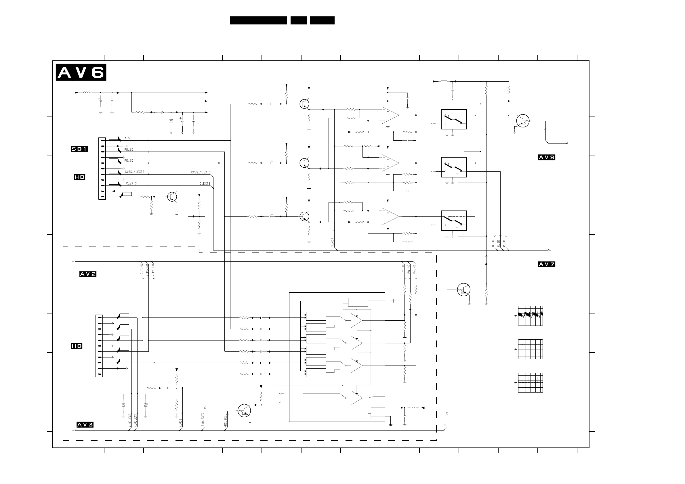
Circuit Diagrams and PWB Layouts
YPBPR RGB Matrix Panel
49F21RE AB 7.
A
B
C
D
E
F
G
H
I
3122 123 60092
123456 10111213
YPBPR-RGB-MATRIX
5655
+8VV
600R
2655
HD1 INPUT
FROM 0304
SD-CONNECTOR
PANEL EUROPE
OR
FROM 0304
HD-CONNECTOR
PANEL USA-AP
USA ONLY
TO HD-MATRIX
1
2
3
4
5
6
7
8
9
10
11
HD2 INPUT
AV300
0300
1
2
3
FROM/TO
0300
HD CONNECTOR
PANEL
TO HD-SYNC-PROCESSING
4
5
6
7
8
9
10
11
12
AV304
0304
100u
2656
F601
F603
F621
F641
F660
F661
H_HD_EXT
V_HD_EXT
G_Y_HD
B_Pb_HD
R_Pr_HD
F655
+8V6
100n
F680
F635
F670
F679
F671
F673
F676
6679
0V
(0V)
BZM55-C5V6
AV3
3666
470R
3635
4K7
AV2
6670
AV3
8V6
+8D
F666
I635
3637
AV2
AV2
3657
100R
BZM55-C5V6
BAS316
10K
I656
6666
7635
BC847B
0V
(0V)
2657
2u2
F667
6667
2665
100u
BZM55-C4V7
3V2
(0V)
+8VV
47K
3655
I655
22K
3656
AV3
2666
I636
5V6
(0V)
4V9
(0V)
+8D
3636
3638
100n
5K6
3K3
AV3
AV7
AV7
Vref3
Vref4
AV2,3
PDTC124EU
0V
(0V)
3673
100R
3671
100R
3677
100R
3675
100R
3681
100R
3679
100R
7690
3602
100R
3642
100R
3622
100R
I673
I671
I677
I675
I681
I679
F690
I604
I641
I621
2673
2u2
2671
2u2
2677
2u2
2675
2u2
2681
2u2
2679
2u2
+8VV
3690
10K
5V3
(0V)
2601
22u
2642
22u
2622
22u
I674
I672
I678
I676
I682
I680
1V2
(0V)
1V2
(0V)
1V2
(0V)
1V2
(0V)
1V2
(0V)
1V2
(0V)
HD2_SELn
I602
I642
I622
3456
789
YPBPR TO RGB MATRIX
22K
22K
(0V)
22K
4V9
(0V)
4V9
4V9
(0V)
7603
BC847B
7643
BC847B
7623
BC847B
+8D
3605
+8D
3645
+8D
3625
8V6
(0V1)
4V3
(0V)
4V3
(0V)
4V3
(0V)
560R
560R
560R
I643
I623
I603
1%
1%
Vref4
1% 1%
3629
3631
1%
470R
1%
3627
3649
3650
Vref4
AV3,7
Vref3
3603
Vref3
3643
Vref3
3623
HD1-HD2-SELECTION
7670
TDA8601T
VIDIa1
VIDIa2
VIDIb1
VIDIb2
VIDIc1
VIDIc2
SEL
FBI1
FBI2
SELECTABLE
CLAMP
SELECTABLE
CLAMP
SELECTABLE
CLAMP
SELECTABLE
CLAMP
SELECTABLE
CLAMP
SELECTABLE
CLAMP
78910111213
2
6
3
7
4
8
5
15
14
3606
1K2
3609
820R
1%
1K
1K2
2K2
1%
DECODING
3610
820R
1%
1%
3651
I626
I646
1K2
3-STATE
3-STATE
3-STATE
3-STATE
I611
3630
I631
I651
0300 G1
0304 B1
2601 A6
2607 A9
2608 B9
2610 A10
2622 D6
I610
5610
+8VV
+8D
100n
4
11
4
11
4
11
1V2
(0V)
1V2
(0V)
1V2
(0V)
8V4
(0V)
7607-A
TSH93
7607-B
TSH93
1%
7607-C
TSH93
2607
I608
7
3V7
(0V)
3608
1%
1K2
2608
RES
I627
8
4V7
(0V)
3626
3K3
3628
390R1K
2628
RES
I647
3V5
14
(0V)
3648
1%
2K2
2648
RES
AV2
AV2
AV2
3684
3688
100R
100R
3686
100R
I685
I683
I687
1K
3683
1K
3685
1K
3687
I670
5670
600R
470n
2670
I607
4V4
5
(0V)
6
4V4
(0V)
(0V)
(0V)
4V6
(0V)
4V6
4V4
(0V)
4V4
Vref4
10
9
12
13
IOCNTR
VIDOa
VIDOb
VIDOc
GND
+8D
+8D
16
12
11
10
13
FBO
1
Vp
9
1K
600R
100n
2610
7610-B
74HC4053D
Y0
2
Y1
115
7610-A
74HC4053D
Y0
12
Y1
13
7610-C
74HC4053D
Y0
5
Y1
3
+8VV
8
Vss
8
0V
(0V)
AV3
16
Vdd
Vee7Vss
E
6
16
Vdd
E
Vee8Vss
7
6
16
Vdd
E
Vee
7
6
7691
PDTC124EU
8V4
(0V)
3615
10K
I615
7615
PDTC124EU
(0V)
0V
AV7,8
FBL_YUV
10K
3611
8V4
(0V)
S
10
Z
(0V)
0V
FROM AUDIO+CONTROL
S
11
8V4
(0V)
1FHn
3691
0V
(0V)
0V
(0V)
F691
RES
AV7
AV7
AV7
TO VIDEO+RC
F601
500mV / div DC
20µs / div
F621
500mV / div DC
20µs / div
F641
2V / div DC
5ms / div
CL 26532118_006.eps
221002
Z
14
S
9
Z
4
2628 C9
2642 C6
2648 E9
2655 A1
2656 A2
2657 H3
A
2665 B3
2666 B4
2670 I9
2671 G6
2673 G6
2675 G6
2677 G6
2679 H6
2681 H6
3602 A6
3603 A6
3605 B7
B
3606 A8
3608 B9
3609 A8
3610 B8
3611 A11
3615 A12
3622 D6
3623 D6
3625 D7
3626 C9
3627 C8
3628 C9
C
3629 B8
3630 B8
3631 C8
3635 C2
3636 D4
3637 D3
3638 D4
3642 C6
3643 B6
3645 C7
3648 D9
D
3649 D8
3650 D8
3651 D8
3655 H3
3656 I3
3657 H3
3666 A2
3671 G5
3673 G5
3675 G5
3677 G5
3679 H5
E
3681 H5
3683 G9
3684 F9
3685 G9
3686 F9
3687 H9
3688 F9
3690 I6
3691 F11
5610 A10
5655 A1
5670 I9
F
6666 A3
6667 B3
6670 I2
6679 I2
7603 A7
7607-A A9
7607-B B9
7607-C D9
7610-A B10
7610-B A10
7610-C D10
G
7615 A12
7623 D7
7635 C3
7643 C7
7670 F6
7690 I5
7691 F11
F601 B2
F603 B2
F621 B2
F635 C2
F641 C2
H
F655 A2
F660 C2
F661 C2
F666 A3
F667 A4
F670 G2
F671 G2
F673 G2
F676 H2
F679 G2
F680 H2
F690 I5
I
F691 E11
I602 A6
I603 A7
I604 A6
I607 A9
I608 A9
I610 A10
I611 B8
I615 A12
I621 D6
I622 D6
I623 D7
I626 B8
I627 C9
I631 C8
I635 C3
I636 D4
I641 C6
I642 C6
I643 C7
I646 D8
I647 D9
I651 D8
I655 H3
I656 H3
I670 I9
I671 G6
I672 G6
I673 G6
I674 G6
I675 G6
I676 G6
I677 G6
I678 G6
I679 H6
I680 H6
I681 H6
I682 H6
I683 G9
I685 F9
I687 G9
Page 50
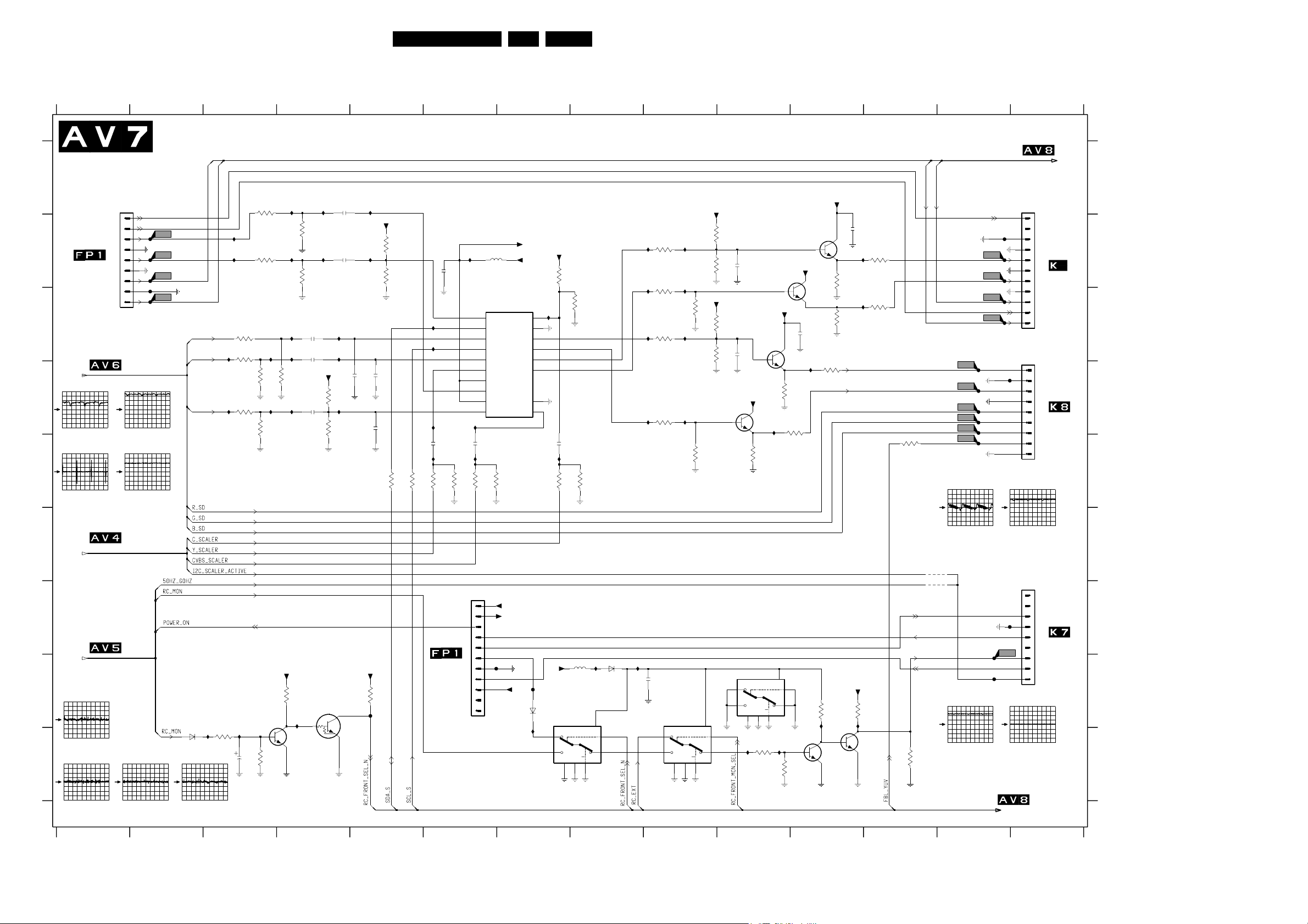
Circuit Diagrams and PWB Layouts
Video + RC Selection Panel
50F21RE AB 7.
12345
A
B
FROM 309
FRONT
PANEL
C
FROM YPBPR-
RGB-MATRIX
F702
D
500mV / div DC
20µs / div
F703
E
50mV / div DC
20µs / div
FROM INPUT
F
FROM
G
OUTPUT
+SUPPLY
H
F706
20mV / div AC
200µs / div
F707
I
20mV / div AC
2ms / div
3122 123 60092
12345
AV309
0309
1
2
3
4
5
6
7
8
9
F704
500mV / div DC
20µs / div
F705
2V / div DC
20µs / div
AV5
AV5
AV5
AV5
F708
20mV / div AC
2ms / div
VIDEO+RC-SELECTION
AV8
AV8
SNDL_FRONT
SNDR_FRONT
F702
F703
F706
F710
F709
16:9_ARFRONT
FRONT_DETECT
CVBS_Y_FRONT
C_FRONT
SNDL_FRONT
SNDR_FRONT
Y_HD1
AV3,6
CVBS_Y_EXT3
AV3
AV3
C_EXT3
AV3
AV3
AV3
AV4
AV4
AV4
AV4
6748
BAS316
F709
20mV / div AC
200µs / div
I748
3748
47K
I728
I730
I702
I704
I749
2748
3707
220R
3715
39R
3717
39R
0V6
(0V6)
10u
3711
39R
3713
39R
3709
3705
7749
BC847B
3749
I729
I731
39R
39R
470K
3708
3750
I711
3710
I713
3706
I707
I715
220R
I717
+5VSTBA
4K7
I750
39R
39R
2707
220n
2715
220n
2717
220n
7751
PDTC124EU
0V
(0V)
I703
I705
+8VT
3719
3721
I726
I716
I718
2711
220n
2713
220n
100K
100K
5V1
(5V1)
2726
I712
I714
220n
3752
3718
3716
2708
220n
220n
2721
+5VSTBA
4K7
F752
AV8
3722
+8VT
100K
100K
100R
AV3,4,8
3723
67891011
YC / CVBS SELECTION
I710
5710
I723
220R
4V3
(0V1)
3V2
(0V2)
3V2
(0V4)
8V8
(0V1)
8V8
(0V1)
11
10
9
8
7
6
5
4
3
2
1
600R
ADRESS 06h
7710
TEA6415CD-TR
10
IN1
2
SDA
20
IN2
4
SCL
1
IN4
5
IN6
7
SUB
11
IN5
9
VCC1
3
IN3
220n
2724
I724
3732
3724
180R
AV308
0308
KEYBOARD
RC_FRONT
F739
(0V)
NC.
8V8
100R
AV3,4,8
I722
I719
2725
3725
100n
2710
4V9
(5V2)
4V9
(5V1)
3V2
(0V2)
3V4
(0V1)
3V2
(0V2)
I725
220n
I727
3733
180R
FROM 0308
FRONT
PANEL
6789
GND1
OUT1
GND2
220R
+5VSTBY
+5VSTB
(3V6)
(5V1)
(1V8)
+8V6
OUT2
OUT3
OUT4
OUT5
OUT6
3V6
5V1
0V2
I742
+8VT
+8VVA
IN7
IN8
6741
3V2
(0V2)
3V2
(3V2)
8
19
13
14
17
18
15
16
12
6
F742
4V6
(4V6)
4V9
(5V1)
BAS316
+8VT
3714
I720
4V8
(0V)
4V8
(0V)
2720
3720
+5VSTBA
7740-C
74HCT4053D
Y0
5
Y1
3
12 13 14
TO AUDIO+CONTROL
AV8
AV8
SNDL_MAIN_OUT
3773
1R
3746
SNDR_MAIN_OUT
4742
4741
RES
KEYBOARD
IR_LED
RC_OUT
ON_OFF_LED
10K
16:9_ARFRONT
CVBS_Y_AV1
C_AV1
SNDL_MAIN_OUT
FRONT_DETECT
SNDR_MAIN_OUT
F727
F726
F770
F771
F772
F773
F770
20mV / div DC
20µs / div
3V3
(3V3)
3V2
(0V)
0V
(0V)
F771
2V / div DC
20µs / div
F704
F705
F707
F708
CVBS_Y_AV2
3V6
(3V6)
0V2
(1V8)
F711
F728
C_AV2
R_SD
G_SD
B_SD
IN_UI_FBL
F740
F743
F772
2V / div DC
NC.
NC.
F741
NC.
F773
2V / div DC
AV333
0333
10
11
AV372
0372
1
2
3
4
5
6
7
8
9
20µs / div
AV341
0341
20µs / div
1
2
3
4
TO 0333
5
6
7
CINCH
8
9
TO 0372
SOURCE
SELECT
9
8
7
FROM/TO
6
5
4
CONTROL
3
2
1
9
0341
TXT &
+8VT
(0V1)
+8VT
8K2
I760
3760
2K2
100K
3712
100K
2V7
(0V)
2V8
(0V)
220n
I721
3730
220R
180R
I739
6740
5740
600R
BAT254
16
Vdd
S
9
Z
4
E
Vee7Vss
6
8
4V9
(5V2)
I740
I762
I764
I766
0V
(0V)
4V8
(4V9)
2740
3762
2K2
3764
2K2
3766
2K2
5V0
(5V0)
100n
7740-B
74HCT4053D
Y0
2
Y1 Z
1
8
I761
I763
I765
I767
Vee7Vss
3728
3726
E
6
16
Vdd
47K
47K
3769
6p8
2K7
3729
2729
4V6
(0V)
+8VT
3767
2V4
(0V)
+8VT
3V9
(0V)
Vee7Vss
3744
7765
BC847B
1K
E
6
10K
I757
16
Vdd
+8VT
S
Z
I745
8K2
3768
6p8
2K7
3727
2727
7767
BC847B
4V6
(0V)
7740-A
74HCT4053D
Y0
12
Y1
13
8
S
10
5V1
I741
15
4V8
(4V9)
7763
BC847B
3765
3757
11
14
0V6
(0V6)
3743
2765
1V8
(0V)
1K
22R
BC847B
22K
2V4
(0V)
7745
+8VT
I756
3V9
(0V)
470n
I746
7761
BC847B
3745
3756
22R
0V
(0V)
10K
3761
3763
7746
BC847B
1V8
(0V)
1K
1K
2761
470n
I754
I755
+5VSTBA
6K8
3747
I747
3754
22R
3755
22R
3V1
(3V1)
TO CONTROL
AV6,8
CL 26532118_007.eps
221002
AV8
AV8
RC- SELECTION
AV8
0308 G6
0309 A1
0333 A14
0341 G14
0372 D14
2707 C4
2708 D5
2710 B6
2711 A4
2713 B4
2715 C4
2717 D4
2720 E7
A
2721 D5
2724 E6
2725 E6
2726 D5
2727 C10
2729 B10
2740 H9
2748 I3
2761 B11
2765 C11
3705 D3
B
3706 B4
3707 C3
3708 D4
3709 D3
3710 B4
3711 A3
3712 C8
3713 B3
3714 B7
3715 C3
3716 B5
3717 D3
C
3718 B5
3719 D4
3720 E7
3721 D4
3722 E5
3723 E5
3724 E6
3725 E6
3726 E9
3727 C9
3728 C9
3729 B9
D
3730 E8
3732 E6
3733 E6
3743 I10
3744 I10
3745 H11
3746 I12
3747 H11
3748 I3
3749 I3
3750 H4
E
3752 H5
3754 B12
3755 C12
3756 D11
3757 D11
3760 B9
3761 B11
3762 C9
3763 C11
3764 C9
3765 D10
3766 D9
F
3767 E10
3768 C9
3769 B9
3773 E12
4741 F12
4742 F12
5710 B6
5740 H8
6740 H8
6741 H7
6748 I2
7710 C6
G
7740-A H10
7740-B H9
7740-C H7
7745 I11
7746 H11
7749 H3
7751 H4
7761 B11
7763 B10
7765 C10
7767 D10
H
F702 B2
F703 B2
F704 B13
F705 B13
F706 B2
F707 C13
F708 C13
F709 C2
F710 C2
F711 B13
F726 D13
F727 D13
I
F728 D13
F739 H6
F740 G13
F741 G13
F742 H7
F743 H13
F752 H5
F770 D13
F771 D13
F772 D13
F773 E13
I702 B3
I703 A4
I704 B3
I705 B4
I707 C4
I710 B6
I711 A4
I712 A5
I713 B4
I714 B5
I715 C4
I716 C4
I717 D4
I718 D4
I719 C6
I720 C7
I721 E7
I722 C6
I723 D6
I724 E6
I725 D6
I726 C4
I727 E6
I728 C3
I729 C3
I730 D3
I731 D3
I739 H8
I740 H8
I741 I10
I742 I7
I745 I10
I746 H11
I747 H12
I748 I3
I749 I3
I750 H4
I754 B11
I755 C12
I756 D11
I757 D10
I760 B9
I761 B9
I762 B9
I763 B9
I764 C9
I765 C9
I766 D9
I767 D9
10 11 12 13 14
Page 51
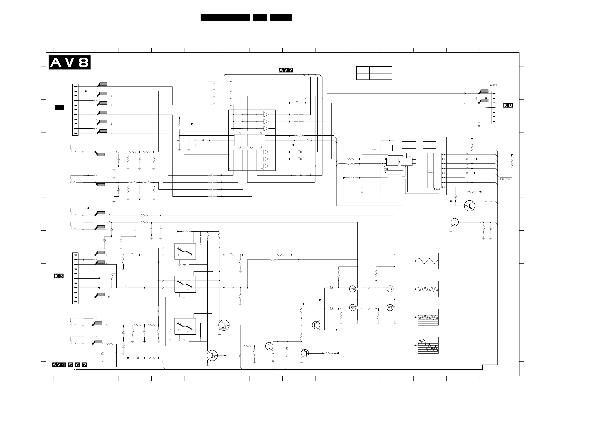
Audio + Control Panel
Circuit Diagrams and PWB Layouts
51F21RE AB 7.
A
FROM 0305
HD
CONNECTOR
B
C
D
E
PANEL
AUDIO_R
VGA_IN
AUDIO_L
VGA_IN
AUDIO_R
MON_OUT
AUDIO_L
MON_OUT
F
FROM/TO
0328
G
SOUND
PROCESSING
H
AUDIO
CENTER IN
RC_EXT_IN
I
CONTROL TO
3122 123 60092
123456789
AUDIO+CONTROL
AUDIO FROM/TO
100n
I840
S
Z
S
Z
S
Z
+8VTEA
2812
2840
11
10
15
9
4
7838
2818
10u
2813
10u
2814
10u
2815
10u
ADRESS 9Ah
I811
22u
2828
*
10u
2829
10u
2830
10u
2831
10u
3854
100n
8V8
(0V1)
0V4
(0V1)
8V8
8V8
(0V1)
0V4
(0V1)
0V
(0V)
I838
47K
3V8
(0V)
11
10
9
8
7
6
5
4
3
2
1
AV302
AV302
AV313
AV313
1
2
3
4
5
6
7
8
9
10
11
AV302
AV313
AV305
0305
0302-A
0302-B
0313-A
0313-B
AV328
0328
0302-C
0313-C
SNDR_HD
F800
SNDR_SD
SNDR_EXT3
SNDL_EXT3
SNDL_SD
SNDL_HD
4
1
5
2
F817
4
1
5
2
F818
NC.
NC.
NC.
NC.
6
3
6
3
0V
(0V)
F816
0V
(0V)
0V
(0V)
0V
(0V)
0V1
(0V)
0V1
(0V)
7V7
(0V)
-6V8
(0V)
(1V8)
0V
(0V)
0V
(0V)
F806
F805
F804
F803
F802
F801
I801
I800
3800
SNDR_VGA
F807
3803220K
6801
I802
BZM55-C33
6802
BZM55-C33
SNDL_VGA
F808
3808
6805
I807
BZM55-C33
6806
BZM55-C33
F809
SNDR_MON
SNDL_MON
F810
6846
BZM55-C33
I856
220K
6847
BZM55-C33
2841
3841
2843
22u
22u
6845
BZM55-C33
F811
SNDR_SSP
F812
SNDL_SSP
+7V7
3842
-7V7
F813
0V
SOUND_ENABLE
1K
33K
3805
1K
33K
6848
I857
2801
I805
2805
3847
150R
3845
150R
BZM55-C33
I841
I843
3801
100p
3806
100p
3K3
3K3
2835
I806
3802
3807
I855
330p
10K
10K
2846
330p
+8VS
5810
2810
+8VS
7840-A
74HC4053D
0V3
Y0
12
(0V3)
0V4
Y1
13 14
(0V4)
8
7840-B
74HC4053D
0V3
Y0
2
(0V2)
0V4
Y1
1
(0V3)
Vss
600R
I810
Vee7Vss
Vee
78
22u
5840
600R
2811
E
6
E
6
16
Vdd
16
Vdd
CENTER-L/R
3851
22u
I854
33K
AV8
SELECTION
7840-C
74HC4053D
Y0
5
Y1
3
VeeVss
7
8
RC_EXT_PRESENT
16
Vdd
E
6
PDTC124EU
F814
F815
6876
SND_CENTER
3876
100R
BZM55-C33
AV7
RC_EXT
6849
BZM55-C33
I852
6850
BZM55-C33
F819
3837
BAS316
3849
33K
6875
2850
I853
3850
1K
1K
100p
2849
I875
I876
3875
47K
1234567
4V4
(0V5)
4V4
(0V5)
4V4
(0V5)
4V4
*
(0V5)
7810
TEA6422D
8V8
(0V1)
I828
*
I829
I830
I831
3852
I850
I845
7853
PDTC124EU
I818
I813
I814
I815
24
R323R420R519R6
R125R2
VS
3
2
CAP
SUPPLY BUS DECODER
GND
1
7
8
NC
21
22
L14L25L36L49L510L6
4V4
(0V5)
4V4
(0V5)
4V4
(0V5)
4V4
(0V5)
AUDIO SELECTION
47K
I844
2842
I842
22u
3848
220K
2844
I846
22u
3846
220K
0V
(0V)
3835
+5VSTBA
10K
AV8
CENTER_SELECT
I835
3836
18
11
(1V2)
150K
7835
BC847B
0V
(0V5)
(0V5)
4V4
(0V5)
4V4
(0V5)
4V4
4V4
ROUT1
ROUT2
ROUT3
SDA
ADDR
LOUT1
LOUT2
LOUT3
I836
SCL
3843
330R
6835
13
15
17
28
27
26
12
14
16
I863
0V
(0V6)
BAS316
3844
330R
4V4
(0V5)
4V4
(0V5)
4V9
(5V2)
8V8
(0V1)
4V4
(0V5)
4V4
(0V5)
4V4
(0V5)
I819
I820
I821
I822
4V9
(5V2)
I826
I827
6862
POWER_VALID
AV7
AV7
AV7
AV7
SNDL_MAIN_OUT
SNDR_MAIN_OUT
I833
5V1
(5V3)
7865
BC857B
5V1
(5V1)
SNDL_FRONT
SDA_S
SCL_S
+5VSTBY
(4V7)
I862
AV3,4,7
AV3,4,7
6868
BAS316
6867
BAS316
0V2
3862
47K
SCL_S
SDA_S
+5VSTBA
3868
I868
I867
I866
MUTE
100R
100R
0V
(0V)
100K
0V
(0V)
0V
(0V)
3867
100K
+5VSTBA
3881
3882
5880
600R
7868
BSH103
7867
BSH103
(0V)
I881
I882
I880
0V
I832
I849
0V5
(0V6)
BAS316
AV5
2819
10u
2820
10u
10u
3822
100R
I824
+8VTEA
10u
10u
I848
I865
2821
3865
3861
SNDR_FRONT
I817
3824
100R
2826
2827
2832
10u
I864
47K
5V1
(4V0)
10K
7862
BC857B
8 9 10 11 12 13 14
10 11
2815
USA only
2828
USA only
7880
PCF8574AT
13
INT_
1
A0
2
A1
3
A2
14
SCL
2880
I871
5V0
(5V3)
100n
BAS316
BAS316
6870
6869
5V0
(5V3)
5V2
(5V3)
I870
I869
15
SDA
16
VDD
8
VSS
ADRESS 78h
0V
(0V)
100K
3870
7870
BSH103
0V
(0V)
7869
BSH103
0V
(0V)
3869
100K
INPUT
FILTER
POWER-ON
0V
(0V)
I/O EXPANDER
INTERRUPT
LOGIC
I2CBUS
CONTROL
SHIFT
REGISTER
RESET
F811
500mV / div AC
200µs / div
F812
I872
500mV / div AC
200µs / div
F821
20mV / div AC
200µs / div
F827
20mV / div AC
200µs / div
12 13 14
LP FILTER
8 BIT
I/O
PORTS
SNDR_SUB_OUT
SNDL_SUB_OUT
4
P0
P1
P2
P3
P4
P5
P6
P7
F884
4V4
(1V8)
5
0V
(0V)
6
0V
(0V)
7
0V
(0V)
9
0V
(0V)
10
5V0
(5V2)
11
12
0V
(0V)
0V
(5V2)
F889
7881
BC847B
F888
7884
PDTC124EU
0V
(0V)
CONFIG_IDENT
+5VSTBA
2K2
3894
F897
F881
SYNC_TRISTATE_MON
F882
F895
RC_FRONT_MON_SEL
3880
10K
5V1
(5V3)
RC_EXT_PRESENT
F821
F825
F827
NC.
NC.
CONFIG_IDENT
RESET_SCALER
HD_VGA_SELECT
CENTER_SELECT
+5VSTBA
RC_FRONT_SEL_N
I889
3883
0373
1
FROM/TO
2
0373
3
4
5
SOURCE
SELECTION
6
7
AV5
+5VSTBA
AV4
AV5
3895
AV5
FBL_YUV
AV8
AV6,7
AV7
AV7
AV8
10u
470K
2883
CL 26532118_008.eps
221002
2K2
0302-A C1
0302-B D1
0302-C H1
0305 A1
0313-A E1
0313-B E1
0313-C I1
0328 F1
0373 A14
2801 C3
2805 D3
2810 C4
2811 C5
2812 C5
2813 A5
A
2814 A5
2815 B5
2818 A5
2819 B8
2820 B8
2821 B8
2826 C8
2827 C8
2828 D5
2829 D5
2830 D5
2831 D5
2832 D8
B
2835 E3
2840 F5
2841 F3
2842 F6
2843 G3
2844 G6
2846 E4
2849 I3
2850 H4
2880 D10
2883 F14
3800 C3
C
3801 C3
3802 C4
3803 C3
3805 D3
3806 D3
3807 D4
3808 D3
3822 C8
3824 C8
3835 I6
3836 I7
3837 I3
3841 F3
D
3842 G2
3843 F7
3844 F7
3845 E3
3846 G6
3847 E3
3848 F6
3849 H3
3850 H4
3851 I4
3852 F6
3854 F5
3861 I8
E
3862 I9
3865 H8
3867 H9
3868 G9
3869 H10
3870 G10
3875 I4
3876 I2
3880 D13
3881 C10
3882 C10
3883 E14
F
3894 C13
3895 C14
5810 B4
5840 E5
5880 D10
6801 C2
6802 D2
6805 D2
6806 E2
6835 I7
6845 F2
6846 E2
6847 F3
G
6848 E3
6849 I3
6850 I3
6862 I8
6867 H9
6868 G9
6869 H10
6870 G10
6875 I3
6876 I2
7810 B6
7835 I7
7838 I5
H
7840-A F4
7840-B G4
7840-C H4
7853 H6
7862 I8
7865 H8
7867 H10
7868 G10
7869 H11
7870 G11
7880 C10
7881 E13
I
7884 D13
F800 A2
F801 B2
F802 B2
F803 B2
F804 B2
F805 A2
F806 A2
F807 C2
F808 D2
F809 E2
F810 E2
F811 F2
F812 F2
F813 G2
F814 H2
F815 I2
F816 D2
F817 E2
F818 F1
F819 I3
F821 A14
F825 A14
F827 B14
F881 C13
F882 D13
F884 E13
F888 D13
F889 E13
F895 D13
F897 C13
I800 C3
I801 C4
I802 C2
I805 D3
I806 D4
I807 D2
I810 C4
I811 C5
I813 A6
I814 A6
I815 B6
I817 B8
I818 A6
I819 B8
I820 B8
I821 B8
I822 C8
I824 C8
I826 C8
I827 C8
I828 D6
I829 D6
I830 D6
I831 D6
I832 D8
I833 D8
I835 I7
I836 I7
I838 H5
I840 E5
I841 F3
I842 F6
I843 G3
I844 F6
I845 G6
I846 G6
I848 F8
I849 F8
I850 G6
I852 I3
I853 H3
I854 H4
I855 F4
I856 F2
I857 F3
I862 I9
I863 I7
I864 H8
I865 H8
I866 H9
I867 H9
I868 G9
I869 H10
I870 G10
I871 H10
I872 H11
I875 I3
I876 I4
I880 D10
I881 C10
I882 C10
I889 E14
Page 52
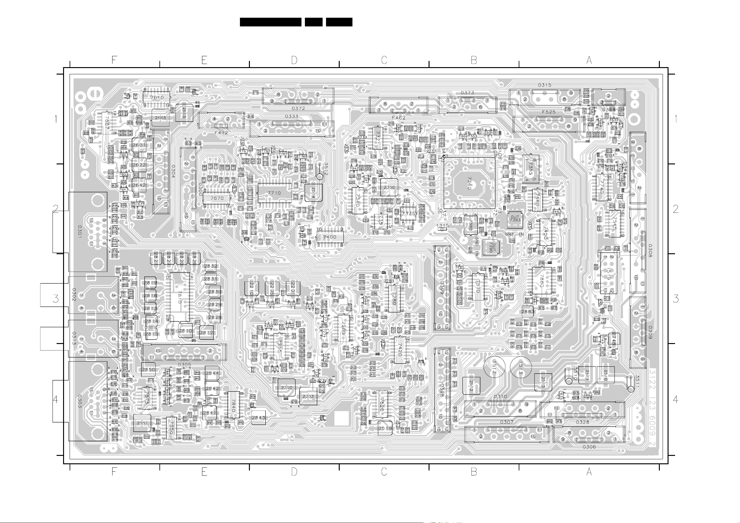
Circuit Diagrams and PWB Layouts
Layout AV Panel (Top Side)
52F21RE AB 7.
3122 123 60092
CL 26532118_009.eps
221002
Page 53

Circuit Diagrams and PWB Layouts
53F21RE AB 7.
Mapping Layout AV
Mapping Top Side Mapping Bottom Side
0300 E2
0301 F2
0302 F3
0303 F4
0304 E2
0305 E4
0306 A4
0307 B4
0308 A2
0309 A3
0310 B4
0313 F3
0315 A1
0328 A4
0333 D1
0340 A1
0341 A2
0355 A1
0370 E1
0371 C1
0372 D1
0373 B1
0398 B4
0399 B3
1315 C1
1340 C2
1341 C2
1342 C2
1512 B4
1513 A4
1519 A3
2201 D3
2205 D3
2210 D3
2215 D4
2227 D4
2250 D4
2251 D4
2252 D4
2253 D4
2255 D3
2257 D4
2259 D4
2260 C3
2274 C3
2275 D3
2280 C3
2281 C3
2282 C3
2283 C3
2284 C3
2285 C3
2286 C3
2303 B1
2304 B1
2307 C1
2311 C2
2312 B1
2313 C1
2320 C1
2321 C1
2322 C1
2330 C1
2333 C1
2340 C2
2350 C2
2351 C2
2352 C2
2353 C2
2360 B1
2361 B2
2362 B2
2363 B2
2364 B2
2365 B2
2366 B2
2367 B2
2368 B2
2369 B2
2370 B2
2371 B1
2372 B1
2373 B1
2375 C2
2376 C2
2377 C2
2380 B2
2385 B1
2390 B2
2391 B2
2393 B2
2394 B2
2400 D2
2420 C4
2421 C3
2423 C4
2425 C3
2427 C4
2429 C3
2431 C4
2450 A2
2451 A2
2460 A2
2510 A4
2511 A4
2512 B4
2513 A4
2514 D2
2515 A1
2520 C4
2521 C4
2522 A4
2523 C4
2524 A4
2525 C4
2526 B4
2527 C4
2528 A3
2529 C4
2530 A3
2531 C4
2532 B3
2534 A3
2536 A3
2538 B3
2542 B3
2545 A2
2546 A2
2550 F4
2551 F4
2570 B3
2571 A1
2575 F4
2585 A1
2587 A1
2588 A1
2601 F1
2607 F1
2608 F1
2610 E1
2622 F2
2628 F1
2642 F2
2648 F1
2655 E1
2656 F1
2657 D3
2665 E1
2666 F1
2670 E2
2671 E2
2673 E2
2675 E2
2677 E2
2679 E2
2681 E2
2707 D2
2708 D2
2710 D2
2711 D2
2713 D2
2715 D2
2717 D2
2720 D2
2721 D2
2724 D2
2725 D2
2726 D2
2727 D2
2729 D1
2740 A2
2748 A3
2765 E1
2801 F3
2805 F3
2810 E3
2811 E3
2812 E3
2813 F3
2814 F3
2815 F3
2818 F3
2819 F3
2820 E3
2821 F3
2826 E3
2827 E3
2828 E3
2829 E3
2830 E3
2831 E3
2832 E3
2835 F4
2840 E4
2841 E4
2842 E4
2843 D4
2844 E4
2846 F4
2849 F3
2850 F4
2880 A3
2883 A3
3201 D3
3202 D3
3203 D3
3205 D3
3206 D3
3207 D3
3210 E3
3211 D3
3212 E3
3215 D3
3216 D4
3217 D3
3218 D3
3223 D4
3224 D4
3225 D4
3226 D4
3227 D4
3228 D4
3229 D4
3230 D4
3231 D4
3232 D4
3237 D3
3238 D4
3239 D3
3240 D3
3241 D4
3242 D4
3250 D4
3255 D3
3257 D4
3259 D3
3260 C4
3265 C4
3267 C3
3269 C3
3270 C4
3271 C4
3272 D3
3273 D3
3274 D3
3275 D3
3281 C3
3282 C3
3283 C3
3284 C3
3285 C3
3286 C3
3287 C3
3288 C3
3289 C3
3296 C3
3297 C3
3301 C1
3303 B1
3304 B1
3305 C1
3307 C1
3308 C1
3309 B1
3310 B1
3311 B2
3312 C1
3313 C1
3314 B1
3315 B1
3320 C1
3321 C1
3322 C1
3323 C1
3324 C1
3325 C1
3326 C1
3330 C1
3331 C1
3332 C1
3333 C1
3334 C1
3335 C1
3336 C1
3342 C2
3343 C2
3344 C2
3345 C2
3346 C2
3347 C2
3352 C2
3353 C2
3354 C2
3355 C2
3356 C2
3357 B1
3358 B1
3359 B1
3360 B1
3376 C2
3377 C2
3378 C2
3379 C2
3380 C2
3381 C2
3386 B2
3387 B2
3400 D2
3410 D1
3419 D2
3421 C3
3423 C4
3425 C3
3427 C4
3429 C3
3431 C4
3432 B4
3433 B4
3434 B4
3435 B4
3437 B4
3440 F2
3441 F2
3442 F2
3444 F2
3445 F2
3446 F2
3447 F2
3452 A2
3453 A2
3461 B2
3462 A2
3510 A4
3511 A4
3512 D2
3519 C4
3520 C4
3521 A4
3522 C4
3523 C4
3525 A3
3526 C4
3527 C4
3529 A3
3530 C4
3531 C4
3533 C4
3534 C4
3535 C4
3536 C4
3537 C4
3538 C4
3539 A2
3540 B3
3541 B3
3542 B3
3543 B3
3544 B3
3545 A2
3546 A2
3547 B3
3548 B3
3550 F4
3551 E4
3552 E4
3553 F4
3554 E4
3555 E4
3556 F4
3557 E4
3558 E4
3559 F4
3560 F4
3561 F4
3562 C4
3563 C4
3564 C4
3565 F4
3566 E4
3567 E4
3569 A1
3570 A1
3571 F4
3572 F4
3573 B3
3574 B3
3575 B3
3576 A1
3577 A1
3578 F4
3579 F4
3580 F4
3581 A1
3582 A3
3583 A2
3584 A1
3585 A1
3586 A1
3587 A1
3588 A1
3589 A1
3591 B1
3592 B1
3593 A1
3594 A1
3595 A2
3596 A2
3597 A1
3598 A1
3599 F1
3602 F1
3603 F1
3605 F1
3606 F1
3608 F1
3609 F1
3610 F1
3611 E1
3615 F1
3622 F1
3623 F2
3625 F2
3626 F1
3627 F2
3628 F1
3629 F1
3630 F1
3631 F2
3635 F2
3636 F2
3637 F2
3638 F2
3642 F2
3643 F2
3645 F2
3648 F1
3649 F2
3650 F1
3651 F1
3655 C3
3656 D3
3657 D3
3666 F1
3671 E2
3673 E2
3675 E2
3677 E2
3679 E2
3681 E2
3683 E2
3684 E2
3685 E2
3686 E2
3687 E2
3688 E2
3690 E2
3691 E1
3705 E2
3706 D2
3707 E2
3708 E2
3709 E2
3710 D2
3711 D2
3712 D2
3713 D2
3714 D2
3715 E2
3716 D2
3717 E2
3718 D2
3719 D2
3720 D2
3721 D2
3722 D2
3723 D2
3724 D2
3725 D2
3726 D1
3727 D2
3728 E1
3729 D1
3730 D2
3732 D2
3733 D2
3743 A2
3744 A2
3745 A1
3746 A2
3747 A1
3748 A3
3749 A3
3750 A4
3752 A4
3754 D1
3755 D1
3756 D1
3757 D1
3760 D1
3761 D2
3762 E1
3763 D1
3764 D2
3765 D2
3766 D2
3767 D2
3768 D1
3769 D1
3773 D1
3800 F3
3801 F3
3802 F3
3803 F3
3805 F3
3806 F3
3807 F3
3808 F3
3822 E3
3824 E3
3835 A4
3836 A4
3837 F3
3841 E4
3842 E4
3843 E4
3844 E4
3845 F4
3846 E4
3847 F4
3848 E4
3849 F3
3850 F4
3851 F4
3852 E4
3854 D4
3861 E4
3862 A4
3865 E4
3867 E4
3868 E4
3869 E4
3870 E4
3875 A3
3876 F3
3880 A3
3881 A3
3882 A3
3883 A3
3894 A3
3895 A3
4408 C4
4410 C4
4412 C4
4450 A2
4451 A2
4519 A3
4520 A3
4521 A2
4741 A3
4742 A3
5250 D4
5274 C3
5280 C3
5303 B1
5321 C1
5340 C2
5350 C2
5385 B1
5400 D2
5420 C4
5450 A2
5513 A1
5520 C4
5523 A4
5525 A4
5529 A3
5531 A3
5535 A3
5537 A3
5545 A2
5550 F4
5570 B3
5575 E4
5585 A1
5610 E1
5655 E1
5670 E2
5710 D2
5740 A1
5810 E3
5840 E4
5880 A3
6250 D4
6251 D4
6275 D4
6296 C3
6297 C3
6322 C1
6334 C1
6340 C2
6440 F3
6441 F2
6442 F2
6444 F2
6445 F2
6450 A2
6462 B2
6463 B2
6513 A1
6559 F4
6560 F4
6561 F4
6570 B3
6571 A1
6578 F4
6579 F4
6580 F4
6581 F4
6582 F4
6583 F4
6584 F4
6595 A2
6666 F1
6667 F1
6670 E1
6679 E1
6740 A1
6741 A2
6748 A3
6801 F3
6802 F3
6805 F3
6806 F3
6835 A4
6845 F4
6846 F4
6847 F4
6848 F4
6849 F3
6850 F3
6862 A4
6867 E4
6868 E4
6869 E4
6870 E4
6875 A3
6876 F3
7202 D3
7206 D3
7211 D3
7215 D4
7230 D4
7246 D4
7255 D3
7257 D4
7259 D3
7260 C3
7265 C3
7267 C3
7269 C3
7271 C4
7272 D3
7273 D3
7274 D3
7275 D4
7280 C3
7296 C3
7301 C1
7302 B1
7303 B1
7304 B1
7305 C1
7321 C1
7340 C2
7341 C2
7347 C2
7351 C2
7360 B2
7375 C2
7380 B2
7385 A2
7390 B2
7393 B2
7400 D2
7419 D2
7420 C4
7435 C4
7450 A2
7453 A2
7460 A2
7520 C4
7540 B3
7545 A2
7546 B3
7550 E4
7568 B3
7570 B3
7571 A1
7573 B3
7575 F4
7587 A1
7589 A1
7603 F1
7607 F1
7610 F1
7615 F1
7623 F2
7635 F2
7643 F2
7670 E2
7690 E2
7691 E1
7710 D2
7740 A2
7745 A2
7746 A2
7749 A3
7751 A4
7761 D1
7763 E1
7765 D1
7767 D1
7810 E3
7835 A4
7838 D4
7840 E4
7853 D4
7862 A4
7865 E4
7867 E4
7868 E4
7869 E4
7870 E4
7880 A3
7881 A3
7884 A3
F204 D3
F205 D3
F206 D3
F208 D3
F209 D3
F210 D2
F215 D2
F216 D2
F217 E2
F218 D1
F222 D1
F227 D2
F232 D1
F236 D2
F240 D1
F250 D1
F251 D2
F253 D1
F255 C2
F268 C2
F269 C1
F270 C1
F302 B4
F306 C3
F309 B3
F311 B4
F312 B3
F313 B3
F314 B3
F321 C4
F326 C3
F336 C4
F341 C3
F343 C3
F350 C3
F353 B3
F355 B3
F370 B4
F371 B3
F380 B3
F381 B3
F391 B3
F394 B3
F408 E4
F409 E4
F410 E4
F411 E4
F412 E4
F429 B1
F430 C2
F431 C1
F432 C1
F433 C1
F434 C1
F435 B3
F436 B2
F437 B2
F438 B2
F439 B1
F440 F3
F441 F3
F442 F3
F443 F2
F444 F3
F445 F3
F460 C4
F461 C4
F462 C4
F463 C4
F464 C4
F501 A2
F502 A4
F503 A1
F504 A1
F505 A1
F506 A1
F507 B1
F508 B1
F509 A3
F510 A1
F511 A1
F512 B1
F513 D3
F514 A1
F515 A3
F516 A2
F520 A4
F521 A4
F522 C1
F523 C1
F524 C1
F525 A4
F526 C1
F528 C1
F529 A4
F530 C1
F533 B1
F534 B2
F559 F1
F560 F1
F561 F1
F562 F1
F578 F1
F579 F1
F580 F1
F581 F1
F584 A4
F585 B4
F590 A4
F596 F3
F597 F4
F598 F4
F599 F4
F601 E4
F602 F4
F603 F3
F621 E4
F622 F4
F641 E4
F642 F4
F643 F4
F655 F4
F660 E3
F661 E3
F662 E4
F663 F4
F666 F3
F667 F4
F702 A2
F703 A2
F704 D4
F705 D4
F706 A1
F707 D4
F708 D4
F709 A1
F710 A1
F711 D4
F726 D4
F727 C4
F728 D4
F739 A3
F740 A3
F741 A4
F742 A3
F743 A3
F752 A1
F770 D4
F771 D4
F772 D4
F773 D4
F800 E2
F801 E1
F802 E1
F803 E1
F804 E1
F805 E1
F806 F1
F807 F2
F808 F2
F809 F1
F810 F2
F811 A1
F812 A1
F813 A1
F814 F2
F815 F1
F816 F2
F817 F1
F818 A1
F819 F2
F821 F3
F825 B4
F827 E3
F879 B3
F880 B3
F881 B1
F882 D1
F883 E3
F884 A1
F885 B3
F886 A3
F887 A3
F888 A2
F889 A2
F890 D3
F891 D4
F892 A3
F893 D3
F894 C3
F895 E4
F896 D3
F897 B2
F898 A3
F899 A3
I201 D2
I202 D2
I205 D2
I206 D2
I210 D2
I211 D2
I215 D2
I219 D1
I225 D2
I230 D1
I233 D2
I237 D1
I260 D2
I261 D1
I262 D2
I263 D2
I264 D2
I265 D1
I266 D2
I267 D2
I268 D2
I269 D1
I270 D2
I271 D2
I272 D2
I273 D2
I274 D2
I275 C2
I276 B2
I277 C2
I279 C2
I280 C2
I281 C2
I282 C2
I283 C2
I285 C2
I286 B2
I287 C2
I289 C2
I290 C2
I291 B2
I292 C2
I293 C2
I294 C2
I295 C2
I296 C2
I297 C2
I299 C2
I301 C3
I302 C3
I303 B4
I304 C3
I305 C3
I306 C3
I307 B4
I308 C3
I309 B4
I310 B4
I315 B3
I322 C4
I323 C4
I324 C4
I325 C4
I331 C4
I332 C4
I333 C4
I334 C4
I341 C3
I342 C3
I352 C3
I353 C3
I354 C3
I355 B3
I356 B3
I357 B4
I358 B4
I359 B4
I360 B3
I383 A4
I384 A3
I385 A4
I386 B3
I387 B3
I400 C2
I401 C2
I402 C2
I403 C2
I404 C2
I405 C2
I406 C2
I407 C2
I408 C2
I409 C2
I410 C2
I411 C2
I412 C2
I415 D2
I416 C2
I417 C3
I418 C2
I419 C2
I420 C2
I421 C2
I422 C2
I423 C1
I424 C1
I425 C1
I426 C1
I427 C1
I428 C1
I429 C1
I430 C1
I431 C1
I432 C1
I435 B1
I436 C1
I440 F2
I441 F2
I442 F3
I443 F2
I450 A2
I451 A2
I452 A2
I453 A2
I454 A2
I455 A2
I456 A2
I460 A3
I462 A3
I510 A3
I511 D4
I512 A1
I513 A1
I519 A2
I520 C1
I521 C1
I523 C1
I525 C1
I527 C1
I529 C1
I531 C1
I533 C1
I534 C1
I535 C1
I540 B2
I541 B2
I543 B2
I544 B2
I545 A3
I546 A3
I547 A3
I548 A2
I549 A2
I550 E1
I552 E1
I553 E1
I554 E1
I555 E1
I556 F1
I557 E1
I558 E1
I559 E1
I560 F1
I561 F1
I562 C1
I563 C1
I564 D1
I565 F1
I566 E1
I567 F1
I568 F1
I569 F1
I570 B2
I571 F1
I572 F1
I573 B2
I574 B2
I575 F1
I576 F1
I577 F1
I578 F1
I579 F1
I580 F1
I581 F1
I582 A4
I583 A4
I584 A4
I585 A4
I586 A4
I587 A4
I588 A4
I589 A4
I590 F1
I591 B4
I592 F1
I593 F1
I595 F1
I596 A2
I597 A3
I598 A3
I599 A3
I602 F4
I603 F4
I604 F4
I607 F4
I608 F4
I621 F4
I622 F3
I623 F3
I626 F4
I627 F4
I641 F3
I642 F3
I643 F3
I646 F3
I647 F4
I702 C4
I703 D3
I704 C4
I705 D3
I707 E3
I710 D3
I711 D3
I712 D3
I713 D3
I714 D3
I715 E3
I716 E3
I717 E3
I718 E3
I719 E3
I720 D3
I721 D3
I722 E3
I723 E3
I724 E3
I725 E3
I726 E3
I727 E3
I728 E3
I729 E3
I730 E3
I731 E3
I739 A3
I740 A3
I741 A3
I745 A3
I746 A3
I747 A3
I748 A2
I749 A2
I750 A1
I751 A1
I754 E4
I755 E4
I756 D4
I757 D4
I760 E4
I761 E4
I762 E3
I763 E4
I764 D3
I765 D4
I766 E3
I767 E4
I800 F2
I801 F2
I802 F2
I805 F2
I806 E2
I807 F2
I810 E2
I811 E2
I813 E2
I814 E2
I815 E2
I817 A1
I818 E2
I819 E2
I820 E2
I821 E2
I822 E2
I824 E2
I826 E2
I827 E2
I828 E2
I829 E2
I830 E2
I831 E2
I832 E2
I833 A1
I835 A1
I836 A1
I840 E1
I841 E1
I842 E1
I843 E1
I844 E1
I845 E1
I846 E1
I848 F1
I849 E1
I850 D1
I851 D1
I852 F2
I853 F2
I854 F1
I855 E1
I856 F1
I857 F1
I862 A1
I863 E1
I864 E1
I865 E1
I866 E1
I867 E1
I868 E1
I869 E1
I870 E1
I871 E1
I872 E1
I875 A1
I876 A1
I880 A2
I881 A2
I882 A2
I884 A2
I885 D4
I886 D3
I887 D4
I890 A3
I891 A3
I892 A3
CL 26532118_10m.eps
221002
Page 54
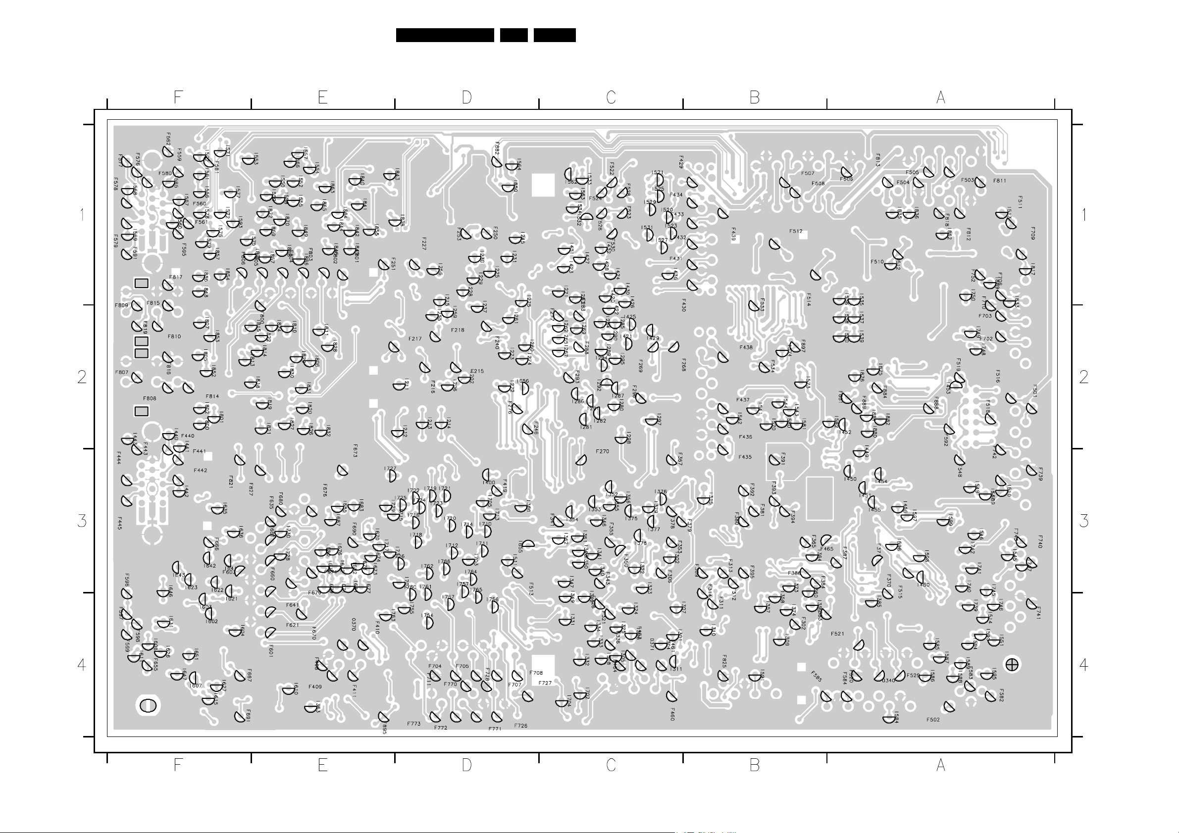
Circuit Diagrams and PWB Layouts
Layout AV Panel (Bottom Side)
54F21RE AB 7.
3122 123 60092
CL 26532118_010.eps
221002
Page 55
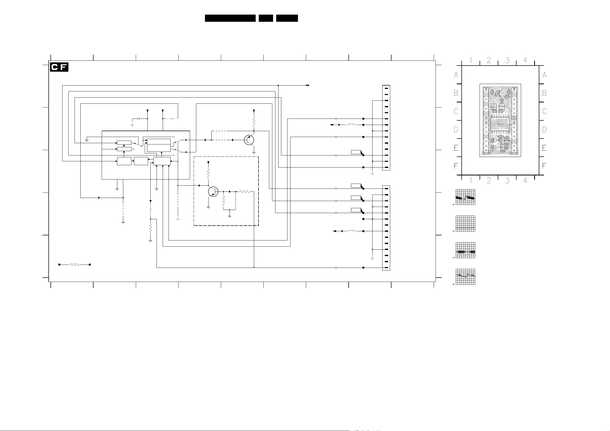
2D Comb Filter Add-on
Circuit Diagrams and PWB Layouts
55F21RE AB 7.
A
B
C
D
5V1
2003
100n
5V0
3001 C4
3002 C5
3003 D3 3999 E1
3004 B5
4001 D2
4002 B4
4003 D3
5000 B8
5001 D8
7000 B5
7001 C4
7002 B2
F001 C8
F002 D8
F003 B8
F004 D8
F005 D8
F006 B8
F007 B8
F008 E8I06 D2
F009 D8
F010 C8
F011 C8
F012 E1
F013 E1
89
0002 C2
(Flying wire to clamp pulse SSP, FTV1.9 only,
GFL SSP Feature lift video processing in 10-7352)
F007
F003
F006
F011
F005
F004
F008
DSM2002-14-PB
1
2
3
4
5
6
7
8
9
10
11
12
13
14
GND
DSM2002-14-PB
14
13
12
11
10
9
8
7
6
5
4
3
2
GND
1
1
1001
VCCAVCCD
SYS2
1K
3004
4002
Y|CVBSO
14
RES
4000
I01
1V5
I02
1V5
COUT 16
OUTSEL
15
10
0V0
NOT
FOR
4003
FTV1.9
GND
1V5
I07
VCCD
3001
0V0
GND
47K
7001
BC847B
FTV 1.9 ONLY
I05
0V0
47K
3000
2001
GND
2V2
BC857B
7000
GND
3002
100K
33p
VCCD
SYS1
Y/CVBS-IN
HA-FTV
Y-OUT
C-OUT
C-IN
FSC
VCCA
I03
5000
10u
F001
F010
F009
F002
I04
5001
10u
To Diagram K1-SSP
Original pinning of IC socket 7560
0003
28
0V0
27
5V1
26
4V2
25
0V2
24
5V0
23
5V1
22
21
0V0
20
0V0
19
0V0
18
1V6
17
16
15
0V3
0002
2V2
14
13
1V5
12
11
0V9
10
9
8
5V1
5V1
7
5V1
6
0V0
5
4
3
4V2
0V0
2
4V2
1
A
B
C
D
E
3122 123 57286
F001
500mV / div DC
10µs / div
F002
500mV / div DC
10µs / div
F009
500mV / div DC
10µs / div
F010
0003 C3
2000 E2
2001 E3
2002 C2
2003 C3
3000 E3
3001 E3
3002 E3
3003 E2
3004 B2
3999 E3
4000 B3
4001 B3
4002 B3
4003 D3
5000 C3
5001 C2
7000 B2
7001 E3
7002 D3
I01 B5
I02 B4
I03 B7
I04 D7
I05 C5
1
I07 C4
I08 C3
0002 C8
0003 A8
1001 A7
2000 D3
234567
2001 D5
2002 B3
2003 B3
3000 D5 4000 B4
2D COMB FILTER ADD-ON
VCCA
2002
GND
0V0
4001
DGND
4
RES
100n
FILTER
TUNING
VCC
GND
5V1
65
VDD
2H/4H DELAY
ADAPTIVE
COMB FILTER
CLOCK
GEN
FSC9FSCSEL
SYS111SYS2
8
0V6
0V0
GND
I08
1n
2000
RES
3003
7002
TDA9181
0V3
0V9
0V3
INPSEL2
Y|CVBS112
Y|CVBS23
CIN1
SC7
I06
13
GND
CLAMP
CLAMP
SAND-
CASTLE
AGND
GND
E
F012
3999
1K
F013
3122 123 57286
123
CL 36532030_004.eps
4
5
678
9
500mV / div DC
10µs / div
040403
Page 56
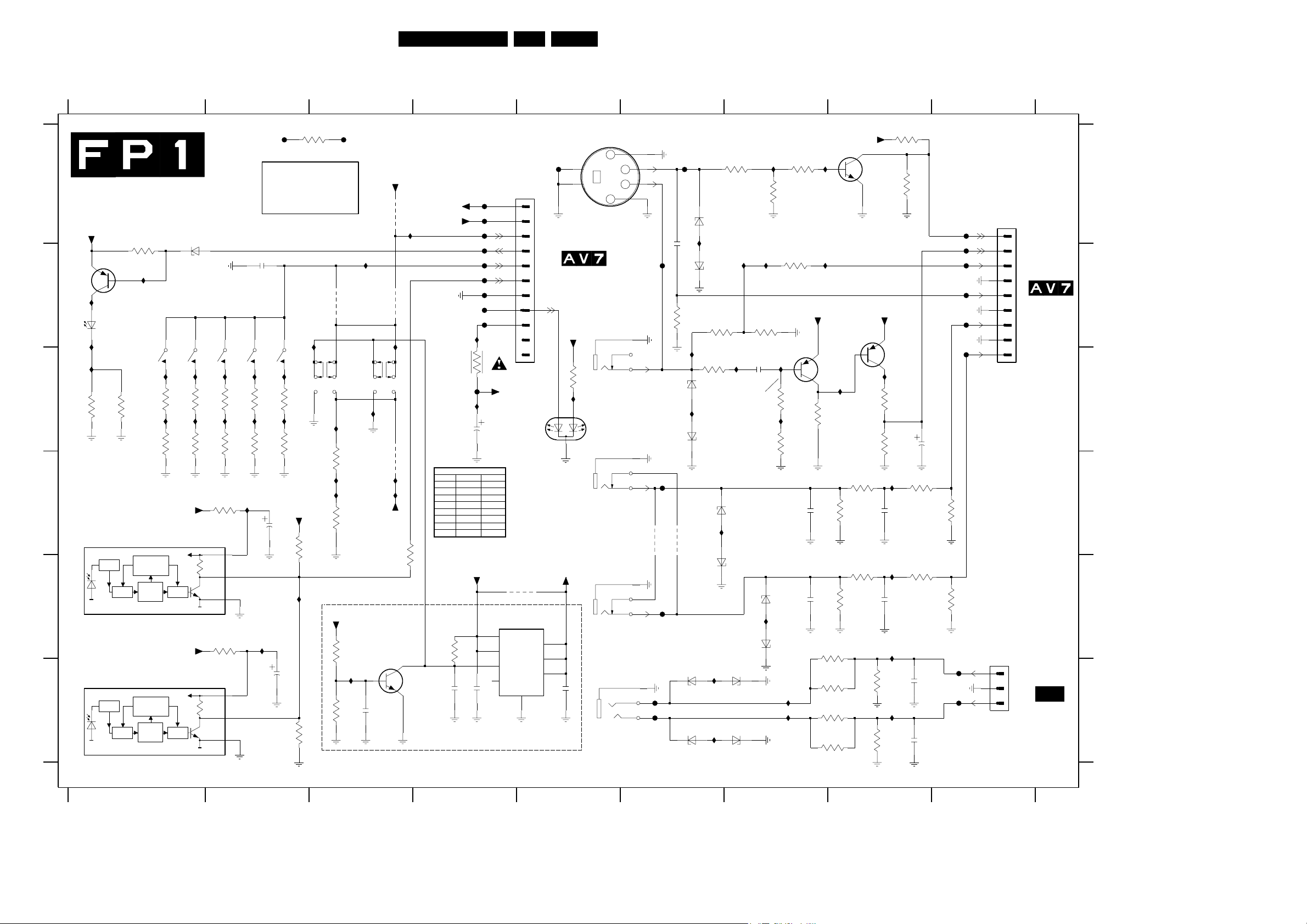
Front Panel
A
Circuit Diagrams and PWB Layouts
56F21RE AB 7.
1
A
FRONT PANEL
+5VSTB
5V3
B
I102
0V2
6002
I104
I103
C
10R
3002
D
6025
TSOP2236
PIN
E
6012
TSOP2236
F
PIN
3001
3K3
I101
7001
BC327-25
IR
LED
TSAL5300
0V
I108
10R
3003
I109
RC-RECEIVER
AGC
CTRL
CIRCUIT
BAND
PASS
INP
RC-RECEIVER
AGC
CTRL
CIRCUIT
BAND
PASS
INP
1
5V2
MENU
1008
3008
3009
+5VSTB
DEM
+5VSTB
DEM
6001
BZM55-C3V3
CH -
1010
I112
I110
1K
1K
3010
I111
I113
1K
3011
100R
OUT
GND
OUT
GND
1012
3012
3013
3025
330R
VS 2
3026
330R
VS 2
2345
CH +
I114
470R
I115
150R
4V9
1
3
4V9
1
3
1014
I155
F098
= On / Off
*
**
= On / Stndby
2005
10n
VOL -
VOL +
1016
I116
3016
3014
100R
I117
3017
3015
100R
100u
2025
5V1
I126
2026
5V1
270R
120R
+5VSTB
3027
I127
100u
3028
3099
10K
**
4
1018
5
6
6K8
10K
I131
I119
I120
RES
**
4007
**
3018
**
3019
8VF
3058
3057
F099
3
I123
I157
1
2
22R
22R
47K
10K
*
I124
1006
0V7
(0V)
2050
I107
4
5
6
I106
I121
I122
100n
+5VSTB
**
4004
*
4005
*
4006
+5VSTB
RES
I105
1
2
3
3029
7050
BC847B
+5VSTBY
+5VSTB
POWER_ON
IR_LED
KEYBOARD
RC_FRONT
Diversity table FP
Item Euro/AP US
1006 x 1018 - x
4004 - x
4005 x 4006 x 4007 - x
7055 x 9024 - x
470R
8V8
(0V1)
F108
3055
2057
I129
100K
0V
10n
3020
2020
5V3
2056
FP308
F126
F100
F101
F102
F103
F104
F105
F106
F107
I128
0308
11
10
9
8
7
6
5
4
3
2
1
1R
8VF
TLUV5300
100u
ON/OFF
STANDBY
LED
+5VSTBY
2
3
4
5
100n
9024
7055
TPS2014P
IN1
OUT1
IN2
OUT2
EN_
OUT3
OC_
GND
1
**
5V SWITCH
FP305
0305
6
F109
5
5V3
5V3
5V2
TO 0308
3V6
3V3
VIDEO +
5V1
RC-SELECTION
ON_OFF_LED
8VF
0V5
(1V8)
3030
560R
6030
I130
1
2
+5VSTB
*
5V3
8
7
6
100n
2055
HEADPHONE
SVHS
0304
FP304
CVBS-Y
0303
FP303
0302
FP303
FP301
0301
67
2
3042
10K
I142
0V
4
3
C
CVBS-Y
F110
3040
4K7
1
6040
BZM55-C33
I141
3041
10K
I140
2040
F111
220n
6041
I146
I145
3048
1R
I144
BZM55-C33
8VF
75R
RES
3043
3
2
1
CVBS-Y
3
3046
I143
3039
100R
6046
I147
BZM55-C33
6047
BZM55-C33
1R
I150
2048
33n
8V6
(0V)
3047
75R
RES
I148
3049
3050
I149
150K
680K
3051
7051
BC857B
I151
8V1
(0V)
39K
2
F112
1
L
L
6060
I160
RES
BZM55-C33
4060
RES
4061
6061
3
BZM55-C33
2
F113
1
R
R
6065
BZM55-C33
I165
6066
6070
1
3
2
F114
F115
BZM55-C33
R_HP
L_HP
6073
BZM55-C33
I171
I172
6071
BZM55-C33
6072
BZM55-C33
BZM55-C33
I134
I135
2060
2065
330p
330p
3070
120R
3071
120R
3073
120R
3074
120R
3061
3066
89
3V2 (0V)
8VF
BC857B
8V3(0V)
3052
3053
I137
2061
I138
2066
I132
10K
3072
I133
10K
3075
3045
5K6
3044
FRONT_DETECT
7052
I152
3K9
2K2
2053
100p
100p
2072
2075
3K3
3062
3K3
3067
3K3
SNDR_FR
8VF
7044
BC847B
CVBS_Y_FRONT
3060
1K
33K
3065
1K
33K
2345678
16:9_ARFONT
C_FRONT
2u2
10n
SNDL_FR
10n
F116
F117
F118
F119
F121
F122
SNDL_FRONT
SNDR_FRONT
10K
3063
10K
3068
F123
F125
FP309
0309
1
3V2
2
3V
3
0V2
4
5
0V
6
7
0V
8
9
0V
FP344
0344
1
0V
2
3
0V
CL 26532054_028.eps
9
TO 0309
VIDEO +
RC-SEL.
TO 0344
M5
AUDIO
240502
4061 D6
0301 F5
0302 E5
0303 D5
0304 B5
0305 A5
0308 A5
0309 A9
0344 F9
1006 C3
1008 C1
1010 C1
A
1012 C2
1014 C2
1016 C2
1018 C2
2005 B2
2020 C4
2025 D2
2026 F2
2040 B6
2048 C7
2050 F3
2053 C8
2055 F5
2056 F4
B
2057 F4
2060 D7
2061 D8
2065 E7
2066 E8
2072 F8
2075 F8
3001 B1
3002 C1
3003 C1
3008 C1
3009 C1
3010 C1
3011 C1
C
3012 C2
3013 C2
3014 C2
3015 C2
3016 C2
3017 C2
3018 D3
3019 D3
3020 C4
3025 D2
3026 E2
3027 D2
3028 F2
3029 D3
D
3030 C5
3039 C6
3040 A7
3041 A7
3042 A7
3043 B6
3044 A8
3045 A8
3046 B6
3047 B7
3048 B7
3049 C7
3050 C7
3051 C7
E
3052 C8
3053 C8
3055 E4
3057 F3
3058 E3
3060 D8
3061 D8
3062 D8
3063 D9
3065 E8
3066 E8
3067 E8
3068 E9
3070 E8
F
3071 F8
3072 F8
3073 F8
3074 F8
3075 F8
3099 A3
4004 A3
4005 B3
4006 D3
4007 B3
4060 D6
6001 B1
6002 B1
6012 F1
6025 D1
6030 C5
6040 A6
6041 B6
6046 C6
6047 C6
6060 D7
6061 E6
6065 E7
6066 E7
6070 F6
6071 F7
6072 F7
6073 F6
7001 B1
7044 A8
7050 F3
7051 C7
7052 B8
7055 E4
9024 E5
F098 A2
F099 A3
F100 A4
F101 A4
F102 B4
F103 B4
F104 B4
F105 B4
F106 B4
F107 B4
F108 C4
F109 A5
F110 A6
F111 B6
F112 D6
F113 E6
F114 F6
F115 F6
F116 A9
F117 B9
F118 B9
F119 B9
F121 B9
F122 C9
F123 F9
F125 F9
F126 A4
I101 B1
I102 B1
I103 C1
I104 B1
I105 A3
I106 C3
I107 C3
I108 C1
I109 C1
I110 C1
I111 C1
I112 C2
I113 C2
I114 C2
I115 C2
I116 C2
I117 C2
I119 D3
I120 D3
I121 D3
I122 D3
I123 C3
I124 B3
I126 E2
I127 E3
I128 B4
I129 C4
I130 C5
I131 B3
I132 E8
I133 F8
I134 F7
I135 F7
I137 D8
I138 E8
I140 A6
I141 A7
I142 A7
I143 C6
I144 B7
I145 B7
I146 B7
I147 C6
I148 C7
I149 C7
I150 C7
I151 C8
I152 C8
I155 D2
I157 F3
I160 D7
I165 E7
I171 F6
I172 F6
Page 57
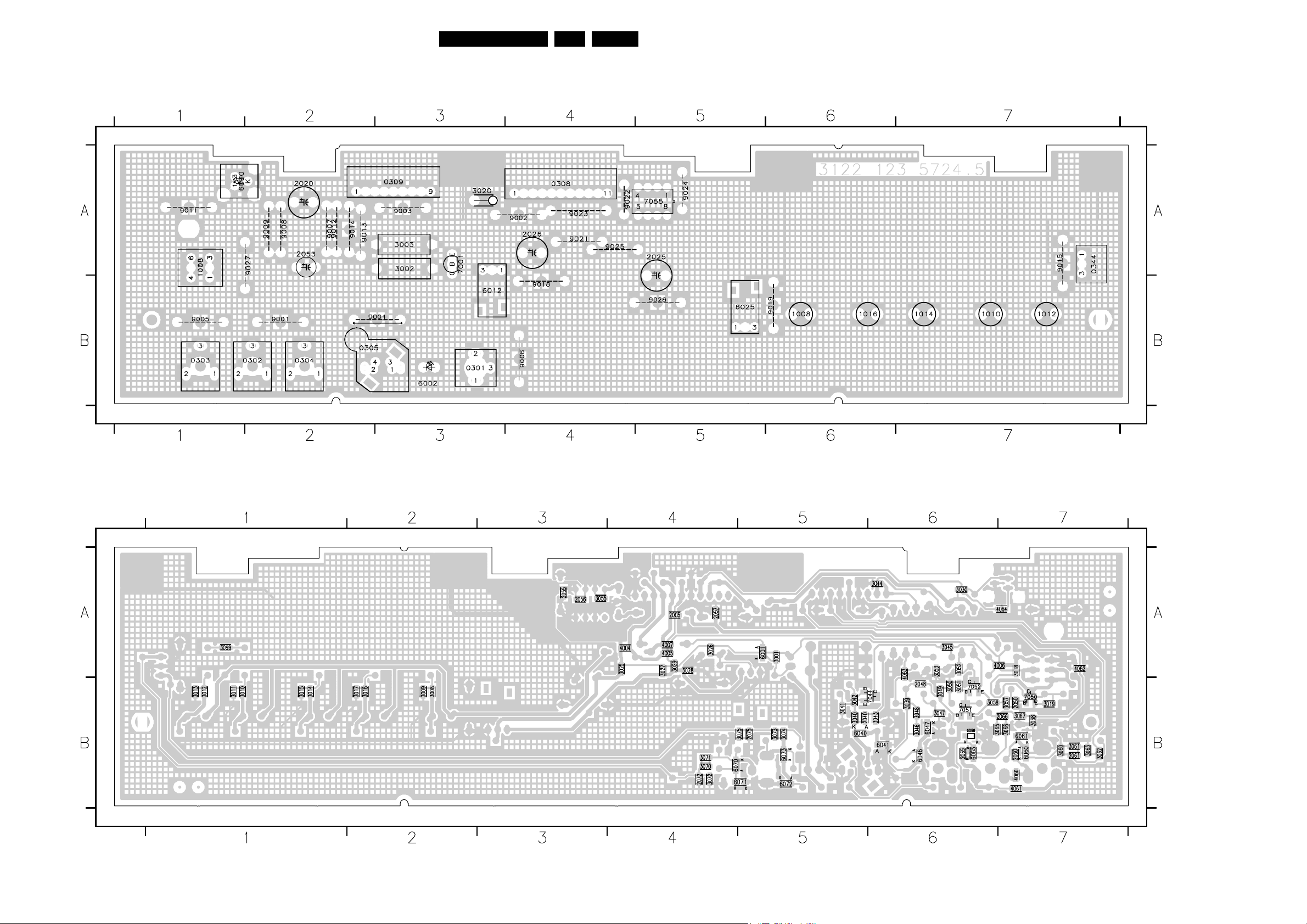
Layout Front Panel
Circuit Diagrams and PWB Layouts
57F21RE AB 7.
Top Side
0301 B3
0302 B2
0303 B1
0304 B2
0305 B2
0308 A4
0309 A3
0344 A7
1006 A1
1008 B6
1010 B7
1012 B7
1014 B7
1016 B6
1018 A1
2020 A2
2025 A5
2026 A4
2053 A2
3002 A3
3003 A3
3020 A3
6002 B3
6012 B3
6025 B5
6030 A1
7001 A3
7055 A5
9001 B2
9002 A4
9003 A3
9004 B3
9005 B1
9006 B4
9007 A2
9008 A2
9009 A2
9011 A1
9012 A2
9013 A2
9014 A2
9015 A7
9018 B4
9019 B6
9021 A4
9022 A4
9023 A4
9024 A5
9025 A4
9026 B5
9027 A2
Bottom Side
CL 26532054_056.eps
220502
2005 A4
2040 B5
2048 B6
2050 B7
2055 A3
2056 A3
2057 A4
2060 B7
2061 B7
2065 B6
2066 B7
2072 B4
2075 B5
3001 A5
3008 B2
3009 B2
3010 B1
3011 B1
3012 B1
3013 B1
3014 B1
3015 B1
3016 B2
3017 B2
3018 A7
3019 B7
3025 A4
3026 A4
3027 A4
3028 A4
3029 A4
3030 A6
3039 B6
3040 B5
3041 B5
3042 B5
3043 B6
3044 A6
3045 A6
3046 B6
3047 B6
3048 B6
3049 B6
3050 B6
3051 B6
3052 A6
3053 A6
3055 A3
3057 B7
3058 B6
3060 B7
3061 B7
3062 B7
3063 B7
3065 B6
3066 B7
3067 B7
3068 B7
3070 B4
3071 B4
3072 B4
3073 B5
3074 B5
3075 B5
3099 A1
4004 A4
4005 A4
4006 A7
4007 A4
4060 B7
4061 B7
4062 A7
4063 A6
4064 A7
6001 A5
6040 B5
6041 B6
6046 B6
6047 B6
6060 B7
6061 B7
6065 B6
6066 B6
6070 B4
6071 B5
6072 B5
6073 B5
7044 B6
7050 B7
7051 B6
7052 B6
Page 58
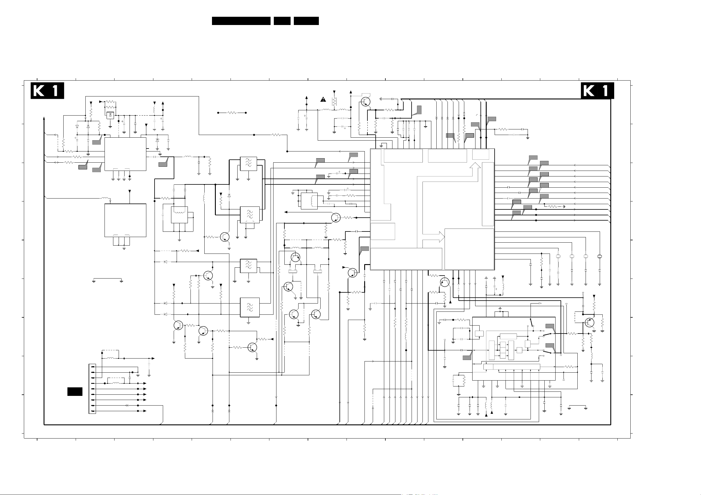
Circuit Diagrams and PWB Layouts
58F21RE AB 7.
Small Signal Board: Tuner IF, Source Selection and Video Processing
2573 I13
2564 I14
2788 H3
2565 F11
3102 A2
2566 F9
3103 B2
2567 G11
3104 B1
2569 H3
3106 C4
2570 H11
3107 D5
2571 I12
3109 E4
2572 I11
220n
*
5102
0u47
68p
10n
2107
2106
*
5103
6
78
7KM
1
2
34
*
*
3109
2K2
I135
*
+5V
3116
2K2
3110
I123
I124
0V
3112
0V7
4K7
0V
I125
*
5K6
3113
*
*
5K6
*
2105
*
+5V
7102
BC847B
3117
2V5
0V
3110 F4
3111 F5
3112 G4
3113 G4
3114 G5
3115 G5
3116 F4
3117 F5
I101
1n5
*
5104
*
5K6
BC847B
3133
6u8
3107
5K6
7103
0V
*
F118
3115
BG
F701
2K7
*
7101
BC847B
*
I134
*
*
I126
5K6
F126
+5V
3134
*
+5V
3111
3114
4K7
3118 C9
3119 D7
3121 G7
3122 G6
3123 G6
3124 B7
3133 B5
3134 C5
*
6105
2K7
2K2
*
*
3999
100R
4105
LMN
BA792
3123
F127
A
B
C
D
E
F
G
H
I
0310 H2
1101 D3
1102 B3
1104 E6
1105 F6
1106 E7
1107 E8
1108 D6
2105 B5
2116 B1
1109 B6
2106 C4
1525 E14
2107 C4
1526 E14
1527 E15
2108 D4
1528 E15
2109 C8
2101 A4
2110 C8
2102 B4
2111 C8
2104 B4
2112 A10
12
2117 D9
2118 D8
2119 A9
2120 A3
2121 B3
2122 D9
2125 B2
2127 A4
2501 F9
2502 F10
2503 F10
2504 F10
2505 F10
2506 F10
2510 C13
TUNER, IF, SOURCE SELECTION and VIDEOPROCESSING
+8V6
+5V
10K
*
2116
3103
100R
6106
BAS216
100u
V14
3102
*
6107
BAS216
10n
2125
V15
GND-1-SEP
F101
0310
1
2
3
4
5
6
7
8
9
*
I1
K2/K8
K2/K7-301
P2-5
*
4112
K7-302
SCL-S
SDA-S
K7-303
LNA
K7-126
8204 000 82671
15K
3140
33K
3141
3104
100R
FROM/TO
AV310 OF
AV5
7113
3146
0V
4V7
4V7
0V
0V
8V6
5V3
5V5
5V5
8V7
33V6
0V7
0V
IN1OUT
L78L05
22K
F132
2
1V6
3
4
5
5109
6u8
2
0V
3
0V
4
0V
5
0V
F102
2511 C13
2512 C13
2520 E13
2521 E13
2522 E14
2525 E14
2526 E14
2527 E15
3154
3155
GND
2
1
3V7
AGC
TU
AS|HIGH
SCL|MID
SDA|LOW
0V
1
AGC
TU
AS|HIGH
SCL|MID
SDA|LOW
4207
6u8
4208
5565
2528 E15
2532 B13
2533 B10
2534 B13
2535 B10
2536 B10
2537 B10
2538 A7
220R
220R
5V
3
F128
2121
4104
*
4V8
6
VSPLL
VSVST
TUNER 1
1102
UV1316
GND
12 13 14 15
0V
6
VSPLL
VSVST
TUNER 2
1101
GND
12 13 14 15
I1455564
6u8
2554 F11
2539 A7
2540 B8
2555 G11
2541 A8
2556 H11
2545 E9
2557 G11
2550 G11
2558 I12
2551 H15
2560 F12
2552 H15
2561 F12
2553 F15
220n
8
0V
8
4114
33V
9
9
2562 I14
+5V
+5V2
F129
6u8
5101
+33V
2101
220u
220n
2127
2102
6101
10
0V
BZX284-C33
2104
11
IF1
0V
10n
I2
*
*
10
0V
11
0V
3106
4R7
F131
2108
*
40.4 TRAP
ALIGNMENT
4101
6102
BA792
2p7
*
*
0V
IF1
345
2120
10u
4V8
7
VTPLL
IF2|GND
*
NC
F116
+5V
4V8
7
VTPLL
IF2|GND
*
NC
0V
*
*
6103
BA792
*
6104
BA792
*
7104
BC847B
+5V2-FB
4n7
F100
10n
2569
I146
F103
F104
F105
F106
F107
2788
+5V2
+5V-STANDBY
+8V6
+33V
+16V
K7-91
STANDBY
3135 G7
3143 A10
3136 D8
3145 F8
3137 D9
3146 B2
3138 D8
3148 E7
3139 E8
3149 F7
3140 B1
3152 A9
3141 B1
3153 B9
3142 A10
3154 A2
678
F702
F119
*
1109
OFWM3953M
1
2
10
1
2
I1
IG
GND
3
GND-IF
*
1108
OFWK6263K
SWI
IN
ING
GND
38
4
O1
5
O2
4
O1
5
O2
3155 A2
3521 E13
3530 B11
3531 B11
3532 B13
3538 A8
3545 F9
3546 G9
3124
100R
K2 OR K9_805
F120
K1_805
3551 G14
3552 G15
3553 G15
3554 F15
3556 H14
3557 G11
3558 H12
3560 F8
2539
+8Vb
F113
100n
1
2
34
I138
*
47R
3119
*
4107
SIFM
F125
F145
*
31485K6
*
I1O
7108
BC847B
*
3149
5K6
BC847B
*
5K6
3121
*
*
4108
G
7106
4110
2
*
10u5105
BC847B
3
1106
TPS
4113
*
*
4111
5K6
1
2
1
2
GND-IF
I1
IG
*
*
1104
OFWM9370M
O1
O2
GND
3
GND-IF
1105
*
OFWK9455M
3
GND-IF
4
5
4
5
3122
2K2
7105
BC847B
+5V
*
*
K3-11
3565 G10
3566 G10
3567 E11
3568 F11
3569 F11
3571 D14
3590 G15
3999 A6
47u
2538
5108
78
7KM
*
7109
*
7107
BC857B
2V3
*
3135
*
4109
4K7
*
6
4102
5106
4u7
1I3
G
I4
I6
8p2
O
2
2V3
4101 E4
4102 D8
4103 B9
4104 B3
4105 G5
4107 G7
4108 G7
4109 G8
5502
6u8
3136
*
*
1107
TPS
*
3145
3538
2V4
220R
I139
*
100R
4110 D7
4111 F7
4112 B1
4113 F7
4114 A3
4207 G2
4208 H3
4803 I9
+8V6
2R2
5501
6u8
22n
2541
47u
2540
2109
2u2
1u
2111
100n
2118
5V4
3V1
7111
BC847B
*
3138
180R
+8Va
7502
BC847B
F133
K2 OR K9-15
CVBS-TER
2110
*
I119
10p
3139
3137
1K
7V5
3560
3118
390R
GHOST-IN
4804 H10
4809 F14
5101 A3
5102 B4
5103 D4
5104 C5
5105 E7
5106 E8
9
+8Va
F130
1K
3153
I3
4.7
4.7
3.7
I5
4.7
4.7
4.3
*
2.7
3.8
2122
3.8
1.5
F124
3.4
2117
4.9
470n
3.4
1K5
I7
3.9
3V4
2545
2V7
3545
470R
470R
3546
K8-500
5108 C7
5109 C2
5501 A8
5502 A8
5540 G10
5553 G15
5559 I12
5560 F13
7112
BC847B
F121
4103
3V3
64
SIF2
63
SIF1
1
AGCSIF
2
VIF1
3
VIF2
4
AGCDEC
6
PLLRILT
7
VCO1
8
VCO2
62
TUNERAGC
10
VIFOUT
12
IN
13
OUT
14
CVBSINT
100n
2566
470R
4803
K8 or K2-502
C-FRONT
2119
330p
3152
100R
5
QSS_AM
IF DEM
GROUP
DELAY COR.
16
3.5
2501
68p
CVBS-SC1-IN
C-7-OUT
K2 OR K9-23
5562 I12
5564 H2
5565 H3
6101 B4
6102 E4
6103 F4
6104 F4
6105 C5
2112
*
3n3
I116
K3-10
3143
*
1K
I100
1K
3142
RES
2533
7V8
0V0
7V8
44
11
45
+8_1
+8_2
GND_19GND_2
SUPPLY
I/O SWITCH
Y_CVBS323Y_CVBS4
CVBS118CVBS2
C3
20
21 24
3.5
0.1
3.5
3.5
100n
100n
2502
2504
100n
2503
I120
1K
3566
CVBS-SC3-IN
Y_CVBS-SC2-IN
SC2-C-IN
K2 OR K9-35
K2 OR K9-45
K8-32
7107 F8
7108 F7
7109 E7
7111 D8
7112 A9
7113 A2
7501 D11
7502 E8
I12
0V0
48
ADSEL
DIGGND
7501
TDA9320H
COMBOUT
CVBSOUT
34
26
3567
3.3
100R
BC847B
3569
47R
CVBS-SC2-OUT
K8 or K5-47
CVBS-TXT-OUT
K2 OR K9-27
7555 G15
7560 F12
7561 F11
F100 H3
F101 G2
F102 H2
F103 H3
F104 H3
STATUS2
STATUS1
K2 or K9-19
K2 or K9-31
0V0
0V0
15
AV117AV2
CTRL
3V4
2V8
7561
3568
2565
150p
2555
100n
CVBS-TXT-OUT
100p
4
19
BG
3
V16
0V0
22
SW0
LUMA & CHROMA PROC.
28
3.5
F141
7V6
470R
+8Vb
F143
2570
2556
6106 B1
6107 B2
7101 D5
7102 E5
7103 G5
7104 G4
7105 G6
7106 G7
10 11 12 13
SIF
K3-9
AM-SOUND
2u2
100n
100n
2537
2535
2536
I117
I118
5V1
4V1
35
33
31
DEC
DIGDEC
PIPOUT
C4
32
2.8
0.1
3.7
100n
2505
100n
2506
100n
I121
3565
100R
1u
5540
F146
4804
CVBS_Y-FRONT
FRONT-C
CVBS-PIP_DS
K8-507
K8 or K2-38
K2 OR K9-36
F105 I3
F106 I3
F107 I3
F108 B12
F109 B12
F110 D13
F111 D13
F112 D13
LMN
K7-48
SCL-F
F122
3530
4V9
46
SW01
( HIP )
YCOMBIN
29
0.1
F142
2554
3557
47R
2567
680p
2557
100n
2550
100n
100n
2572
K7-49
SDA-F
F123
3531
100R
4V9
47
SCL
SDA
SYS127SYS2
CCOMBIN
25
0.0
5.1
100n
1V2
I122
1V2
1V7
V18
1V7
1M
10u
2571
F113 A7
F116 C3
F118 C5
F119 B6
F120 B7
F121 A9
F122 A11
F123 A12
100R
V17
4V1
58
30
0.1
7560
SAA4961
5
24
17
10
19
3558
4V6
I114
K5 OR K8-51
S1
F108
0V0
61
HPLL
SYNC
SVBCOUT
59
0
REFBP
VREF
REFDL
YEXT/
CVBS
CEXT
CSY
VDDD
22
10u
2558
F124 D9
F125 E7
F126 I5
F127 I6
F128 A3
F129 A4
F130 A9
F131 D4
VA
HA
K5 OR K8-52
F109
0V3
60
VA
HA
R1IN
G1IN
B1IN
FBL1IN
R2IN
G2IN
B2IN
OUTP SWITCH
FBL2IN
YOUT
UOUT
VOUT
X3.579
X3.575
X3.582
X4.43
COL_PLL
SEC_DEC
SCOUT
100n
27
VCCPLL
DGND
21
4V5
5559
100n
+5V2
+5V2
S2
2560
6u8
36
37
38
39
41
42
43
40
49
50
51
57
56
55
54
52
53
47u
26
PLLGND
DELAY LINES
VCCA
7
6u8
1V2
2V0
2V2
0V0
2V2
2V0
2V2
0V0
2V7
2V3
2V2
2V5
2V5
2V5
2V5
5V2
0V1
I113
AGND
9
5562
2561
F132 B2
F133 F8
F141 F11
F142 F11
F143 G11
F144 F15
F145 I7
F146 G10
3532
15K
+5V2
6u8
IC14IC2
DELAY
BPFBPFBPF
BYP
2573
2510
100n
2512
100n
CLOCK CONTROLSYNC
3
3V7
5560
16
10u
2534
4n7
V3a
V3c
CORRELATOR
SSYN
2
IC3
6
4V5
2511
100n
I115
F701 A5
F702 A6
I100 A10
I101 B5
I110 G15
I111 G15
I112 H15
I113 F12
2532
1u
V3b
28
IC4
BPF
FSCR
13
V1a
V1c
V2a
V2c
2520
15
CVBSO
SUM
SYS120SYS2
0V
I114 H12
I115 H13
I116 A10
I117 B10
I118 B10
I119 C8
I120 F10
I121 F10
F110
F111
F112
100n
I137
V1b
V1d
V2b
V2d
I136
3521
2521
HA-FTV
18
LPFI0N
COMBENA
VCCO
23
4V5
4V5
2562
100K
100n
8
2522
V19
V20
100n
I122 G12
I123 F4
I124 F4
I125 G4
I126 G5
I134 E5
I135 E5
I136 E14
10K3571
3n3
YO
CO
FSC
OGND
11
1525
2525
14
1V8
12
1v3
25
1
14
3V8
3V7
2564
4M33619
HC49U
18p
Y-CB-OUT
C-CB-OUT
3556
FSC
680p
GND-IF
I137 E13
I138 D7
I139 E8
I145 H3
I146 H3
1526
2526
3551
270R
10K
1527
HC-49/U
3MHZ582056
18p
K5 or K8-400
N_52502
2553
BC857B
4809
1V8
*
3552
K5 OR K8-602
K5 OR K8-601
K5 OR K8-600
K2-22
FBL-SC1-IN
K5 OR K8-603
SC2-R-IN_C-IN
K5 OR K8-604
K5 OR K8-605
K5 OR K8-606
FBL-SC2-IN
K5 OR K8-55
K5 OR K8-54
K5 OR K8-53
HC-49/U
18p
2527
+8Va
3554
100n
F144
I110
150R
RES
I111
68u
I112
*
2552
15
R-SC1-IN
G-SC1-IN
B-SC1-IN
G-SC2-IN
B-SC2-IN
Y-DEC
U-DEC
V-DEC
1528
3MHZ575611
2528
1K
2V4
7555
3590
0V
*
3553
*
5553
*
6p8
2551
3M579545
HC-49/U
15p
820R
10p
A
B
C
D
E
F
G
H
I
12
345
678
9101112
13 14 15
CL 36532030_006.eps
030403
Page 59
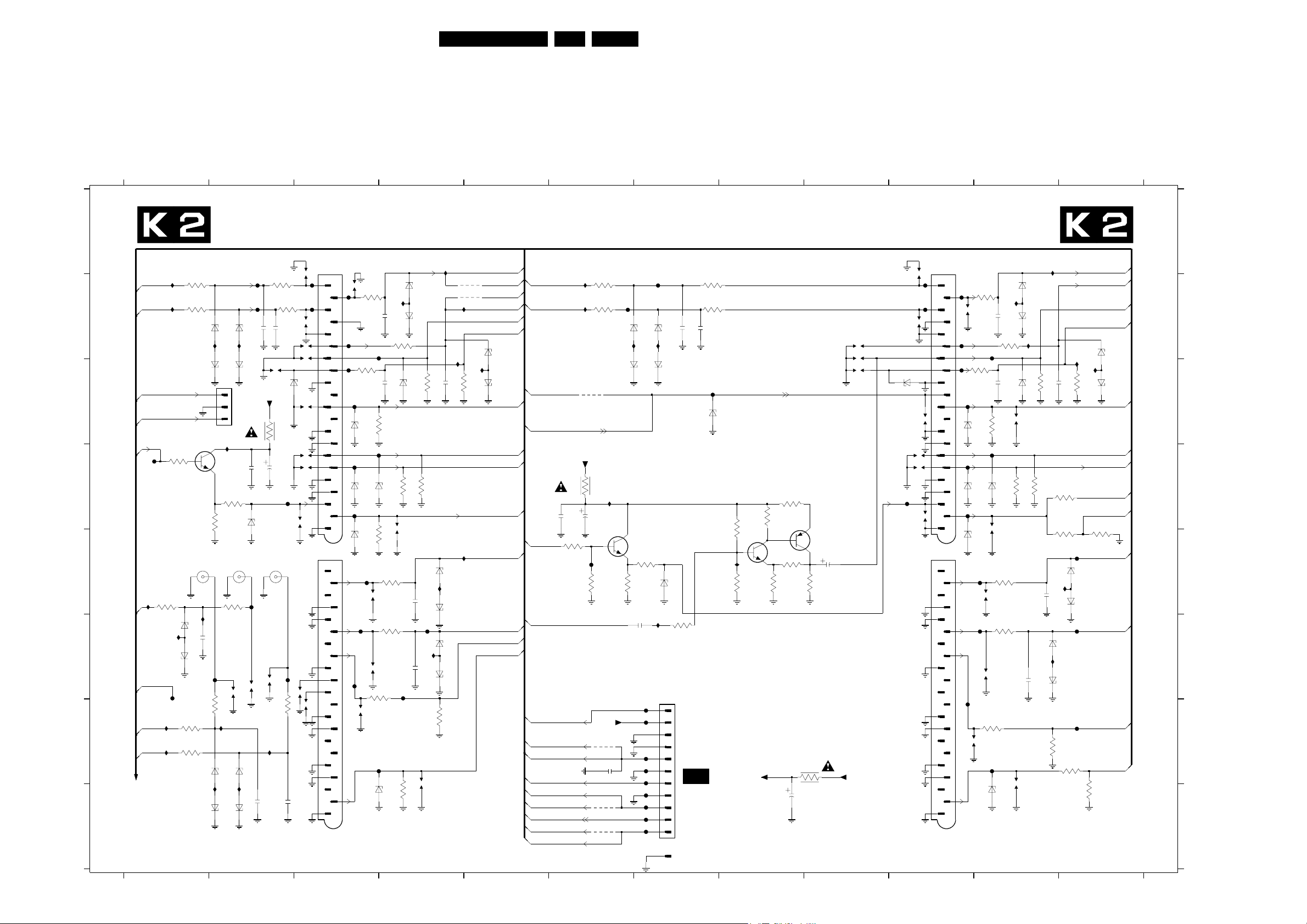
Small Signal Board: Input/Output
0333 F7
0376 H8
0381 C2
1200-A E1
1200-B E2
1200-C E2
1201-A A3
1201-B E3
1202-A A10
1202-B E10
2126 H8
2202 B2
2203 B2
2204 D2
2205 D2
2206 B4
2209 C4
2210 C4
2212 E6
2213 E6
2215 B7
2216 B7
2217 B11 3243 F9
2218 G6
2219 C11
2220 C11
2221 F7
2222 F9
2224 E4
2226 F4
1
2228 H2 3252 F8
2229 H2 3253 F8
2235 F1
2240 E11
2241 F11
3147 G9
3200 B1
3201 B1
3202 B2 3265 G4
3203 B2
INPUT / OUTPUT
A
Circuit Diagrams and PWB Layouts
3204 C2
3205 D1
3206 D2
3207 D2 3273 G11
3208 E12
3209 E3
3210 D4
3211 D4
3212 E12
3213 C3 4227 H6
3215 C4
3216 C4
3218 C3
3219 B4
3220 B3
3221 B6
3222 B6
3223 B7 6203 C2
3224 B7 6204 D2
3225 D6
3227 G12
3228 E6
3229 F6
3230 F6
3231 H12
3232 E7 6211 D3
3233 G1
3235 D11
3236 D11
3240 C11
3241 C11 6216 B7
3242 C12
3244 B11
3245 C11
3246 B11
3247 F8
3248 F8
3249 F8
3250 F7
3254 E4
3255 F4
3256 H4
3257 G2
3258 G2
3264 F4
3266 F8
3270 E11
3271 F11
3272 G1
3274 G11
3280 E2
3826 E1
4201 C6
4226 H6
59F21RE AB 7.
4228 G6
4229 B5
4230 B5
4235 D12
6200 B1
6201 C1
6202 B2
6205 B4
567
6206 B4
6207 C4
6208 B5
6209 C5
6210 C3
6212 D3
6213 E3
6214 B6
6215 C6
6217 C7
6218 C7
6219 D7
6220 B11
6221 B11
6222 C11
6223 B12
6224 C12
6225 C10
6226 D10
6227 D11
6228 E10
6229 E4
6230 E4
6231 F4
6233 H3
6234 G1
6235 H1
6236 G2
6237 H2
6239 C10
6240 E12
6241 E12
6242 F11
6243 F11
6244 H11
6259 C2
6260 F1
6261 F1
7200 D2
7201 E6
7203 F9
7204 F8
F300 B3
F301 B3
F302 B3
F303 B3
F304 B4 F314 B10
F305 C3
F306 C3
F307 D4
F308 D3
F309 D2
F310 D3
F311 B10
F312 B10
F313 B10
8
F315 B11
F316 C10
F317 C10
F318 D11
F319 D10
F320 D10
F321 C7
F322 D10
F323 F2
F324 F2
F325 G7
F327 G7
F328 G7
F329 G7
F330 H7
F331 H7
F332 H7
F333 E3
F335 G4
9
F336 F3
F337 F7
F338 E10
F339 F11
F340 G11
F341 G11 I321 E1
F342 E12
F343 F12
F344 G12
F346 G1
F347 G7
F348 F4
F349 D1
F506 E2
I300 A4
I301 A11
I302 B26232 F4
I303 B7
I304 B4
I305 B2
10 11234
I306 B6
I307 B11
I308 B4
I309 B12
I310 C2
I311 E6
I312 E4
I313 E6
I314 F4
I315 G2
I316 F8
I317 G2
I318 F1
I319 G1
I320 G1
I322 B1
I323 B1
I324 B6F334 F3
I325 B6
I326 F7
I327 B1
I328 B2
I329 B4
I330 C5
I331 B6
I332 B7
I333 F1
I334 H1
I335 H2
I336 E4
I337 F4
I338 B11
I339 C12
I340 F11
I341 E12
12
A
B
C
D
E
F
G
H
8204 000 81015
SNDR-SC1-OUT
K8 or K3-13
SNDL-SC1-OUT
K8 or K3-14
SNDR-CL_VL-OUT
K3-100
SNDL-CL_VL-OUT
K3-101
CVBS-TER
K1-15
F349
SNDS-VL-OUT
K4+K3-23
I321
150R
SNDS-VR-OUT
K1-22
SNDR-CL_VL-OUT
K3-100
SNDL-CL_VL-OUT
K3-101
K1 / K8
SCART 1
1201-A
1A
F300
F302
3A
5A
7A
9A
BZX284-C12
11A
13A
15A
17A
19A
21A
SCART 3 K8-505
1201-B
1B
3B
5B
7B
9B
11B
150R
13B
15B
17B
19B
330p
21B
62026203
BZX284-C10
I328
BZX284-C10
CINCH-OUT
SOUND
I310
3206
68R
560R
6204
YKC21-2675
6
1200-C
3280
150R
150R
6236
BZX284-C10
I335
6237
BZX284-C10
I302
I305
330p2202
BZX284-C10
BZX284-C10
3204
2204
100n
2205
BZX284-C6V8
LEFT
YKC21-2675
52
3
1200-B
F506
I317
BZX284-C10
2229
330p
BZX284-C10
3203
150R
3202
150R
330p
2203
6259
+8V6
6R8
10u
F309
F324
3257
2228
3200
150R
I322
3201
150R
I323
6200
I327
6201
1
2
3
0381
3205
470R
3826
6260
I333
BZX284-C10
F346
I320
I319
12
7200
BC547B
3207
RIGHT
YKC21-2675
41
1200-A
I318
3n3
BZX284-C10
2235
6261
F323
3258
I315
3272
150R
3233
150R
6234
I334
6235
2A
4A
6A
8A
10A
12A
14A
16A
18A
20A
2B
4B
6B
8B
10B
12B
14B
16B
18B
20B
6239
F322
SCART 2
1202-A
F311
1A
F313
3A
5A
7A
9A
11A
13A
15A
17A
19A
21A
SCART 4
1202-B
1B
3B
5B
7B
9B
11B
13B
15B
17B
19B
21B
2A
4A
6A
8A
10A
12A
14A
16A
18A
20A
2B
4B
6B
8B
10B
12B
14B
16B
18B
20B
F312
F314
F316
F317
6225
F319
6226
F320
6228
F338
3246
1K
F315F304
3245
3K9
3240
BZX284-C6V8
F318
6227
BZX284-C6V8
BZX284-C6V8
F339
F340
3273
8K2
F341
6244
I338
2217
100p
3244
1K
2219
330p
75R
3236
BZX284-C6V8
3270
1K
3271
1K
BZX284-C6V8
6220
6221
I307
6222
75R
2241
I301
BZX284-C10
BZX284-C10
3241
2220
150R
BZX284-C6V8
75R
3235
4235
100R
3208
39R
I341
2240
100p
6242
I340
6243
100p
3274
2K7
I300
75R
6229
6230
6231
6232
3265
2210
4229
4230
I304
I308
3216
100p
I312
BZX284-C10
BZX284-C10
BZX284-C10
BZX284-C10
2K7
F301
3220
1K
F303
3218
3K9
F305
F306
6210
BZX284-C6V8
F308
6211
BZX284-C6V8
F310
6213
BZX284-C6V8
F333
F334
F336
3
2206
2209
3213
F307
6212
3209
3254
3255
3264
8K2
F335
6233
6205
I329
BZX284-C10
6206
100p
BZX284-C10
3219
1K
3215
330p
6207
BZX284-C6V8
75R
75R
75R
3210
3211
BZX284-C6V8
75R
1K
1K
BZX284-C6V8
I336
2224
100p
I314
I337
2226
100p
F348
75R
3256
4567
IN-SC1-SNDR
SNDR-SC1-IN
SNDL-SC1-IN
IN-SC1-SNDL
K5 or k8-18
IN-SC1-B
STAT U S 1
6208
I330
8K2
6209
IN-SC1-G
K5 or K8-20
IN-SC1-R
K5 or K8-21
FBL-SC1-IN
CVBS-SC1-IN
SNDR-SC3-IN
K8 or K3-42
K8 or K3-43
SNDL-SC3-IN
CVBS-SC3-IN
K8 or K1-38
K8-16
K3-16
K3-17
K8-17
K1-19
BZX284-C10
BZX284-C10
K1-22
K1-23
P2-6
K7-44
K1-45
K1-36
K8-509
K8-39
K3-39
K7-40
K3-41
K8-41
K3-24
SNDR-SC2-OUT
K3-25
SNDL-SC2-OUT
16:9-ARFRONT
C7-26
IO-BUS
K7-201
2213
K1-27
CVBS-SC2-OUT
C-7-OUT
K1-502 or K8-502
16:9-ARFRONT
CVBS_Y-FRONT
FRONT-Y_CVBS
FRONT-C
IN-FRONT-SNDL
SNDL-FRONT-IN
FRONT-DETECT
SNDR-FRONT-IN
IN-FRONT-SNDR
100n
3228
I324
I325
3225
100R
4201
2212
+8V6
I313
3229
3221
150R
3222
150R
6R8
10u
4228
4226
4227
I311
10K
+8V6
2218
150p
I306
I331
3230
6214
6215
7201
BC547B
3232
560R
2221
220n
F337
F325
F347
F327
F328
F329
F330
F331
F332
I303
6216
BZX284-C10
I332
6217
BZX284-C10
68R
6219
I326
OR 1K5 IF 4 SCARTS
0333
1
2
3
4
5
6
7
8
9
10
11
0376
1
2216
330p
BZX284-C10
BZX284-C10
BZX284-C6V8
3250
100R
FROM/TO
AV333 OF
AV7
2215
3224
150R
3223
150R
F321
6218
330p
BZX284-C6V8
10K
3266
I316
2K7
3249
K1_805
BZX284-C12
3252
33R
3253
390R
7203
3247
100R
RES
330R
2126
47u
3243
3147
10R
BC557B
2222
47u
150R
+8V6
7204
BC847B
3248
8 9 10 11
SNDR-SC2-IN
SNDL-SC2-IN
I309
8K2
3242
100p
K5 OR K8-33
IN-C_IN-R-SC2
K5 OR K8-34
Y_CVBS-SC2-IN
IN-SC2-CVBS_Y
F342
SNDR-SC4-IN
6240
BZX284-C10
6241
BZX284-C10
F343
SNDL-SC4-IN
BZX284-C10
BZX284-C10
F344
3227
CVBS-SC4-IN
39R
3231
K8 or K3-28
K8 or K3-29
K5 OR K8-30
IN-SC2-B
K1-31
STATUS2
6223
I339
BZX284-C10
6224
IN-SC2-G
K5 OR K8-32
IN-SC2-FBL
K1-35
K8-35
3212
39R
K8-504
P2-5
K2 or K7-301
K8-1
39R
12
BZX284-C10
CL 36532030_007.eps
030403
B
C
D
E
F
G
H
Page 60
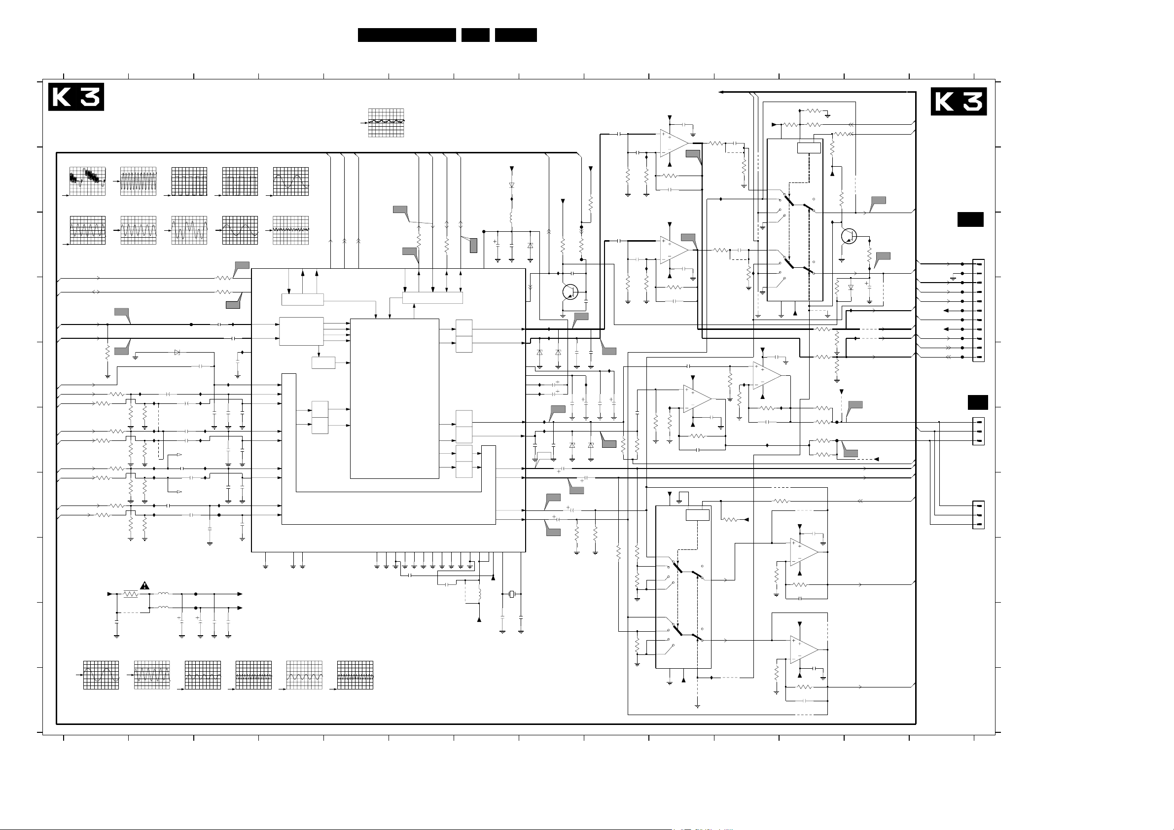
Circuit Diagrams and PWB Layouts
Small Signal Board: Sound Processing
12
SOUND PROCESSING
A
I14
BZX284-C10
4u7 2802
4805
4806
2761
220n
5751
6u8
5752
6u8
I2S-CL/7-7751
1V / div DC
5µs / div
A12 (audio)
2V / div
0.2ms / div
I402
6751
4u7
2803
2804
220n
HCC-R
K8-130
2806
2807
220n
220n
HCC-L
K8-130
2762
220n
2765
100u
A22
2753
220n
I406
I407
2754
I411
I412
220n2805
I414
I415
2763
F413
F414
2766
2810
100u
SC1-R/48-7751
1V / div DC
0.5ms / div
2801
22p
I416
I417
3756
100R
3755
100R
470p
I15
A13
470p
2n2
B
C
D
E
F
G
H
I
J
I11
SIFM-E7111
0.5V / div DC
10µs / div
A8 (ssp)
0.5V / div
0.2ms / div
K7-94
SCL-F
K7-95
SDA-F
K1-11
SIFM
K1-9
SIF
3781
K1-10
AM-SOUND
K2 or K9-16
SNDR-SC1-IN
K2 or K9-17
SNDL-SC1-IN
K8 or K2 or K9-28
SNDR-SC2-IN
K8 or K2 or K9-29
SNDL-SC2-IN
K8 or K2 or K9-42
SNDR-SC3-IN
K8 or K2-43
SNDL-SC3-IN
K2 or K9-41
SNDR-FRONT-IN
K2 or K9-39
SNDL-FRONT-IN
3785
6K8
3789
6K8
3793
6K8
3753
6K8
+5V2
A20a
2V / div
0.2ms / div
8204 000 82671
12
I12
0.2V / div DC
A12
I11
I12
560R
3784
6K8
3788
6K8
3792
6K8
3754
6K8
4n7
SIF/Pin5-7501
5µs / div
0.5V / div
0.2ms / div
I418
22K
3786
3787
22K
3791
3790
22K
3794
3795
22K
3752
3751
3750
2R2
4704
2787
A21a
0.2ms / div
I419
22K
I420
I421
22K
I422
I423
22K
I424
I425
22K
2V / div
34
I2S-WS/6-7751
A7 (ssp)
MSP-CLOCK
1V / div DC
10µs / div
0.5V / div
0.2ms / div
A26
4V0
4V9
A27
I427
2751
100n
I426
2752
I405
3V2
0V0
3V2
2756
2755
470p
3V2
3V2
2758
2757
470p
3V2
3V2
2760
2759
470p
3V2
3V2
2764
0V0
1V5
1V5
9
8
23
25
24
47p
28
30
31
470p
33
34
470p
36
37
470p
39
40
470p
0.5V / div
0.2ms / div
A14
HP-R/1-0344
50mV / div DC
0.5ms / div
DEMODULATOR
15 16 1718192
10
0V
ADR
68
3
ADR-CL
ADR-DA
interface
7751
MSP3410D 1
I2C_CL
I2C_DA
ANA_IN2+
ANA_IN1+
ANA_IN
MONO
MONO-IN
SC1-IN-R
SC1-IN-L
SCART 1
SC2-IN-R
SC2-IN-L
SCART 2
SC3-IN-R
SC3-IN-L
SCART 3
SC4-IN-R
SC4-IN-L
SCART 4
0V
IDENT
A/D
A/D
41
K4-111
ADR-WS
53 5455
SELECT_TO_EXT2
1
2V5
AUD_CL_OUT
62 63 64
+5DA
+5DB
1n
2811
A23
SC1-L/47-7751
1V / div DC
0.5ms / div
A24
SC2-R/51-7751
1V / div DC
0.5ms / div
A25
1V / div DC
0.5ms / div
34
60F21RE AB 7.
567
A15
HP-R/3-0344
50mV / div DC
0.5ms / div
I2S-CL
I2S-DSP-OUT1
K4-116
K4-117
3841
100R
2V4
0V
7
4
I2S_CL
I2S_DA_IN1
I2S-WS
2V4
6
I2S_WS
D/A
D/A
I15
SELECT_AUDIO_LR
K4-113
0V
0V
14
13
D_CTR_OUT0
D_CTR_OUT1
FM1
FM2
NICAM A
NICAM B
IDENT
S1...4
I2SL/R
I2S-DSP-IN
K4-114
I14
3839
I13
2V4
65
5
I2S_DA_IN2
I2S
I2SL/R
LOUDSPEAKER R
LOUDSPEAKER L
K4-115
100R
I2S_DA_OUT
interface
DSP
SCART-L
AHVSS
43
VREF1
49
ASG3
52
D/A
D/A
D/A
D/A
VREF2
DVSS
58
66 67
SCART-R
SCART
Switching Facilities
ADR_SEL
DACM_SUB
12
TESTEN
AVSS
22
27
HEADPHONE R
HEADPHONE L
SCART-R
SCART-L
ASG1
ASG2
ASG4
32
35
38
2897
100n
1n
2898
4862
6u8
SC2-L/50-7751
567
+8V6
6757
8V4
45
AHVSUP
DACM-R
DACM-L
DACA-R
2808
VREFTOP
AGNDC
CAPL_M
CAPL_A
5753
2809
100u
RESETQ
F412
LOUDSPEAKER
HEADPHONE
DACA-L
SC1-OUT-R
SC1-OUT-L
SCART 1
SCART 2
SC2-OUT-R
SC2-OUT-L
DVSUP
XTAL_IN
AVSUP
STANDBYQ
26
11
2V2
4V9
4V9
1751
+5DA
5759
HC-49/U
18M432
3p3
2767
+5DB
MCL4148
I442
6u8
1n
61
2768
XTAL_OUT
2021
8
RESET-AUDIO-INV
K4-118
6752
BZX284-C10
I430
7774
BC847B
5V
I403
0V5
57
I404
0V5
56
6754
6753
BZX284-C10
29
2V2
42
I437
7V2
44
I438
7V5
46
10u
2777
A20
I409
0V
60
I410
0V
59
1n
2786
2785
A22
48
3V3
47
3V2
A24
51
3V3
2849
50
3V2
10u
A25
2V2
3p3
8
+5DB
3832
2890
220n
BZX284-C10
10u2778
1n
2846
10u
2848
K7-93
1K
2773
2779
6755
A23
10u
3799
+5DB
RESET-AUDIO
3840
F416
10K
3833
F417
2891
A7
1n
2774
I428
100n
2780
6756
BZX284-C10
2847
10u
47K
910
11 12
K1:K8
+7V7
2775
470n
3844
2901
10n
47K
I432
7756-B
LM833DT
3780
6K8
2770
10n
5
8
6
4
-7V7
3760
68K
2776
68p
A21a
3820
7
100R
I400
2844
4740
1u
K2 or K9-22
3828 47K
SNDS-VL-OUT
SNDS-VR-OUT
10K
+7V7
10u
3852
22K
3845
6K8
2900
10n
47K
2784
22K
3770
3771
3772
I431
0V
3761
470n
3853
6K8
15K
15K
7756-A
6K8
3847
1
-0V1
5
0V
2
0V
4
0V
12
0V
14
15
0V
11
0V
3
2
A20a
8
LM833DT
4
2771
10n
-7V7
3758
68K
2772
68p
2783
470n
7757-A
MC33178D
3
0V
I433
2
0V
-7V9
-7V7
47K
10K
3766
+7V7
7V2
16
9
VDD
7752
HEF4052BT
LL
LH
HL
HH
LL
LH
HL
HH
VEE
VSS
0V
7
8
-7V9
-7V7
1
+7V7
8
4
3765
68K
2790
22p
0V
10
LOGIC
6
2845
3827
100R
1u
4741
47K3829
I401
+7V7
7V2
5
0V
I434
6
47K
3846
0V
1
0V1
3768
10K
2793
10n
0V4
LSBMSB
4K7
3773
+7V7
H
L
3
0V
H
13
L
0V
I444
0V
4810
4811
100n
1n
I429
10u
2781
BZX284-C10
47K
3798
A8
100n
A21
2769
470n
2782
3769
91011
I443
3899
+7V7
K2/K4 or K9-120
VDD
4738
7753
RES
HEF4052BT
LL
1
5
LH
HL
23
4
HH
4730
12
LL
LH
14
15
HL
HH
11
VSS
8
4739
2792
10n
8
MC33178D
7757-B
4
-7V9
-7V7
I408
3767
68K
2791
22p
I413
1R
3897
4K7
916
10
LOGIC
3898
100R
LSBMSB
+7V7
3762
3782
100R
4K7
SELECT_AUDIO_CINCH_2
SELECT_AUDIO_CINCH_1
4702
H
6K8
2K7
3800
BC847B
7773
SNDL-CL_VL-OUT
I439
47K
3802
220K
I441
SNDR-CL_VL-OUT
6759
BAS216
13
I435
4700
I436
4701
1K
3893
L
H
L
VEE
6
7
-7V7
4801
3892
3890
2K7
1K
3830
120R
3796
120R
3797
120R
3831
120R
3891
F411
F410
+7V7
4726
A15
A14
SNDR-HEADPH-OUT
SNDL-HEADPH-OUT
4725
7
0V
4720
3783
100R
7758-A
LM833DT
-0V1
-0V1
56K
3777
4812
+7V7
2798
10n
3
8
1
3776
33K
2800
-0V2
4
-7V9
-7V7
2
SELECT_TO_EXT2
22p
+7V7
7758-B
LM833DT
3779
+7V2
5
8
0V
6
0V
4
-7V9
-7V7
56K
3778
33K
2799
22p
4721
2797
10n
4813
7
-0V2
12 13 14
13 14
K4-112
K4-12
A12
K2 or K9-100
I440
K4-24
K4-98
AUDIO-R
K4-97
K4-122
K4/K3-98
AUDIO-R
K4/K3-97
AUDIO-L
K4-128
SNDS-VL-OUT
K4-28
AUDIO-C
+7V7
K3-29
HP-GND
-7V7
K4-125
AUDIO-SW
K7-103
SOUND-ENABLE
K7-102
DC-PROT
A13
3801
K2 or K9-101
4703
2869 220u
AUDIO-R-PROC
AUDIO-L
AUDIO-L-PROC
HP-GND
-7V7
HP-GND
SNDR-SC1-OUT
K8 or K2-13
SNDL-SC1-OUT
K8 or K2-14
K3-110
K2 or K9-24
SNDR-SC2-OUT
K2 or K9-25
SNDL-SC2-OUT
FROM/TO
AV328 OF
AV7
0328
F400
1
F420
2
F401
3
F402
4
F403
5
F404
6
F405
7
F406
8
F407
9
F408
10
F409
11
FROM/TO
AV344 OF
FP
0344
1
K3-29
2
3
NC.
0348
1
2
3
CL 36532030_008.eps
030403
0328 C14
0344 F14
0348 G14
1751 H7
2751 D3
2752 E3
2753 E3
2754 F3
A
2755 F3
2756 F3
2757 F3
2758 F3
2759 G3
2760 G3
2761 G2
2762 G2
2763 G3
2764 G3
2765 I2
2766 I3
B
2767 I7
2768 I7
2769 C9
2770 A10
2771 C10
2772 D10
2773 E8
2774 E9
2775 A9
2776 B10
2777 E8
C
2778 E8
2779 E8
2780 E8
2781 E9
0V
2782 E9
2783 E10
0V
2784 F9
0V
2785 F8
2786 F8
0V
2787 I1
2790 F10
0V
2791 F11
D
7V3
2792 E11
2793 F10
0V
2797 I12
2798 G12
-7V3
2799 J12
2800 H12
0V
2801 D3
0V4
2802 E2
2803 E2
0V
2804 F2
2805 F2
2806 F2
E
2807 G2
2808 C7
2809 C7
2810 I3
2811 I3
2844 A11
2845 C11
2846 F8
2847 F9
2848 G8
2849 G8
2869 D13
F
2890 C8
2891 D8
2897 H6
2898 H6
2900 C9
2901 B9
3750 H2
3751 G1
3752 G2
3753 G1
3754 G1
3755 D3
G
3756 C3
3758 D10
3760 B10
3761 D9
3762 B12
3765 F10
3766 F10
3767 E11
3768 E11
3769 H9
3770 H9
3771 H9
H
3772 I9
3773 G11
3776 H12
3777 H11
3778 J12
3779 J11
3780 B9
3781 E1
3782 A12
3783 G11
3784 E1
3785 E1
I
3786 F1
3787 F2
3788 F1
3789 F1
3790 F1
3791 F2
3792 F1
3793 G1
3794 G1
3795 G2
3796 F12
J
3797 F12
3798 G9
3799 G8
3800 B13
3801 C13
3802 D12
3820 A11
3827 C11
3828 B11
3829 D11
3830 E12
3831 F12
3832 C8
3833 C8
3839 C6
3840 B9
3841 C6
3844 B9
3845 D9
3846 E11
3847 F10
3852 F9
3853 F9
3890 E12
3891 E12
3892 D12
3893 D12
3897 A12
3898 A12
3899 A12
4700 D13
4701 D13
4702 B13
4703 D13
4704 I2
4720 G11
4721 J12
4725 F13
4726 E12
4730 C11
4738 B11
4739 D11
4740 B11
4741 C11
4801 D12
4805 F2
4806 F2
4810 J11
4811 J10
4812 G12
4813 I12
4862 H7
5751 H2
5752 I2
5753 C7
5759 H7
6751 E2
6752 C8
6753 E8
6754 E8
6755 F8
6756 F9
6757 B7
6759 D13
7751 C3
7752 G10
7753 B11
7756-A C9
7756-B A9
7757-A E10
7757-B E12
7758-A G11
7758-B I11
7773 C13
7774 D8
F400 C14
F401 D14
F402 D14
F403 D14
F404 D14
F405 D14
F406 D14
F407 D14
F408 E14
F409 E14
F410 F12
F411 F12
F412 C7
F413 H3
F414 I3
F416 C8
F417 C8
F420 C14
I400 B11
I401 D11
I402 D2
I403 D8
I404 D8
I405 E3
I406 E3
I407 E3
I408 E12
I409 F8
I410 F8
I411 F3
I412 F3
I413 F11
I414 F3
I415 F3
I416 G3
I417 G3
I418 E2
I419 E2
I420 F2
I421 F2
I422 F2
I423 F2
I424 G2
I425 G2
I426 E3
I427 D3
I428 E8
I429 E9
I430 C8
I431 C9
I432 B9
I433 E10
I434 E11
Page 61
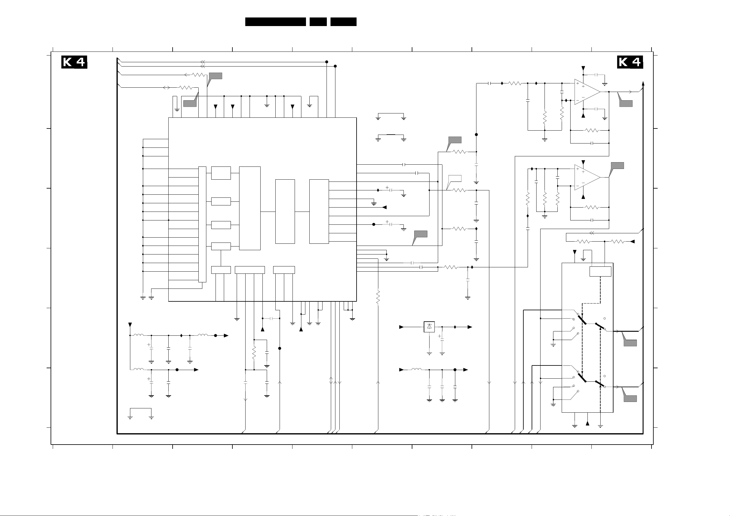
Small Signal Board: Audio Dolby
1
SELECT_AUDIO_CINCH_1
SELECT_AUDIO_CINCH_2
I2S-DSP-OUT1
AUDIO DOLBY
K7-306
A
B
C
D
E
F
123
SDA-F
+3V3S
5754
6u8
GND-DIG
5755
6u8
8204 000 82671
Circuit Diagrams and PWB Layouts
23
K3-12
K3-13
1
MIC
I509
10n
10n
3818
100R
A29
2
VDACP2
100R
A28
3838
+5DC
5V2
5V2
22
46
36
21
SDA
ADC-CLK
VDDD5V1
IIS-IO-OUT1
MTC
AD
SCAD1
SCAD2
SCAD3
ANALOG SOURCE SELECT
DEMOD
TSCAN
60
F503
5758
1u
10n
2825
+3V3SA
+3V3SD
3V3
50
54
53
VSSD3V2
VSSD3V4
VDDD3V2
MIC
STEREO
AUDIO
XTAL OSC I2C
SHTCB
SRC3-R
OSC-IN62OSC-OUT
65
59
1V6
+3V3SD
2836
K3-111
MSP-CLOCK
49
VSSD3V1
63
+3V3SD
3817
47p
K3-17
7770
SAA7712
GND-DIG
2816
100u
2818
100u
GND-DIG
74
75
76
2815
2817
VSSA1
VREFAD
VDACP1
VDACN23
RECOUTRV4
VDDA173
SRCO-L72
SRCO-R71
SRC1-L70
VDACN177
SRCOUT-R78
SRC2-R67
SRC3-L66
SRC1-R69
SRC2-L68
TUNER-MPX80
SRCOUT-L79
VSS-OSC61
GND-DIG
F505
61F21RE AB 7.
45 89
F507
F508
+3V3SD
5V2
47
37
RDS-SCK
IIS-IO-OUT2
55
23
VSSD3V5
VSSD5V1
51
52
VSSD3V3
VDDD3V1
48
RDS-DATA
0V
40
DSP-IN138DSP-IN2
DSP-OUT1
39
41
DSP-OUT2
5
RECOUTRI
OUT2-I 11
OUT3-I 10
OUT1-V 16
VREFDA 15
VSSA2 13
VDDA2 14
EMSCB QDAC
OUT3-V 9
POM
8
RECOUTLI 6
RECOUTLV 7
12
OUT2-V
43
VSSD5V3
44
A0
45
SCL
17
OUT1-I
18
OUT0-I
19
OUT0-V
20
OV
VDDD5V2
VDDD5V3
VDD-OSC
DSP-RESET
64
5V2
3V3
2895
57
RTCB
58
VSSD3V6
VSSD5V2
IIS-IO-WS
IIS-IN1-BCK
IIS-IN1-DATA28IIS-IN1-WS
IIS-IN2-BCK
29
2V5
27
2V5
IIS-IN2-DATA25IIS-IN2-WS
26
24
IIS-IO-BCK
IIS-IO-IN1
IIS-IO-IN2
56
33
30
31
32
34
42
35
2V5
10n
+5DC
F504
RES
100K
2835
2812
RES
K3-114
K3-116
K3-117
K3-118
RESET-AUDIO-INV
I2S-CL
I2S-DSP-IN
I2S-WS
456
67
GND-S2
A15a
3812
100R
A16a
3814
100R
3813
100R
3811
100R
1V6
1V6
1V6
1V6
3V3
1V6
F500
1V6
1V6
1V6
1V6
I510
3819
2824
100u
+3V3SA
2831
100u
100R
GND-S1
2827
1n
2822
1n
2829
1n
A17a
2820
1n
7750
+5DC
+5V2
+5V
5756
6u8
LF33CV
IN OUT
GND
2837
3V3
10n
2819
2813
I502
100u
F502
10n
2814
+3V3S
10n
K7-307
SCL-F
CN:
7
I501
2821
+5DC
2823
RES
2830
2828
10n
F501
10n
I503
10n
7772-A
+7V7
LM833DT
I504 I505
2841
470n
3848
100R
2832
22n
3842
I506
47K
RES
3821
3
2834
2
6K8
-7V7
GND-S1
56K
+7V7
5
6
-7V7
I507
3849
2833
100R
22n
3894
2851
47K
3825
I508
GND-S2
470n
2892
3824
100R
+7V7
VDD
7775
HEF4052BT
LL
1
5
LH
HL
23
4
HH
12
LL
LH
14
15
HL
K3-128
K3-125
AUDIO-SW
89
K3-121
K3-122
AUDIO-R-PROC
AUDIO-L-PROC
SNDS-VL-OUT
K3-124
AUDIO-C
HH
11
VSS
7
8
2839
10n
8
1
4
2840
10n
3822
68K
2838
22p
8
7
7772-B
4
LM833DT
3837
56K
2826
22p
SELECT_AUDIO_LR
916
10
LSBMSB
LOGIC
VEE
6
-7V7
SNDS-VL-OUT
H
L
H
L
CL 36532030_009.eps
10
K2/K3-120
A18a
A50
K3-113
3823
4K7
K3-98
AUDIO-R
K3-97
13
AUDIO-L
10
+7V7
A51
A52
K1 / K8
030403
A
B
C
D
E
F
2812 F4
2813 F7
2814 F7
2815 E2
2816 E2
2817 F2
2818 F2
2819 E7
2820 D7
2821 D7
2822 D7
2823 B8
2824 B6
2825 E3
2826 C10
2827 B6
2828 C8
2829 B7
2830 C8
2831 C6
2832 A8
2833 B9
2834 A9
2835 E4
2836 F4
2837 F7
2838 B10
2839 A10
2840 A10
2841 A8
2851 B9
2892 C8
2895 E4
3811 D7
3812 B7
3813 C7
3814 B7
3817 E4
3818 A3
3819 D6
3821 A9
3822 A10
3823 C10
3824 C9
3825 C9
3837 C10
3838 A3
3842 A9
3848 A8
3849 C8
3894 C9
5754 E2
5755 E2
5756 E7
5758 E3
7750 E7
7770 A2
7772-A A9
7772-B B9
7775 D9
F500 C6
F501 B8
F502 E7
F503 E3
F504 E4
F505 E3
F507 A5
F508 A5
I501 D8
I502 E7
I503 C8
I504 A8
I505 A9
I506 A9
I507 B9
I508 C8
I509 E3
I510 B6
Page 62
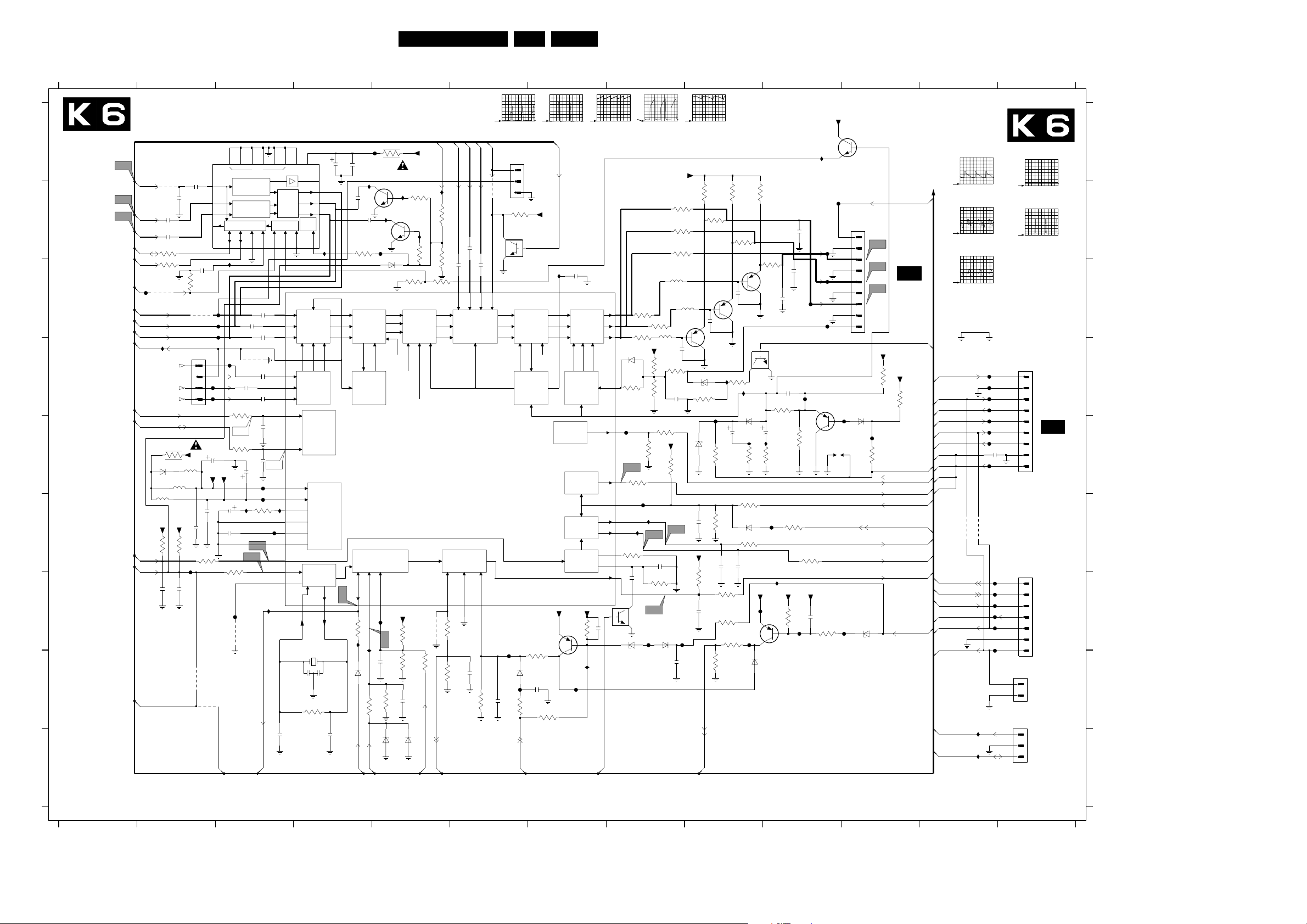
Circuit Diagrams and PWB Layouts
Small Signal Board: Video Control and Geometry
12
VIDEO CONTROL & GEOMETRY
A
7402
2413
100n
6u8
3308
2308
2
TOPIC
2414
100n
RES
3421
1
2
3
4
5300
RES
1K
F632
10p
2417
4429
0364
+8V6
2301
4427
1V5
1V5
100n
RES
3317
4426
TDA9178
1V3
6
8
9
22
F646
F647
F648
F650
F651
2300
220u
2302
100n
1K
YIN
UIN
VIN
CF
4V5
+8VS
100n
HFB
F1K
K8 OR K5-201
Y-FEAT
3436
F2K
K8 OR K5-202
2415
U-FEAT
B
C
D
E
F3K
K8 OR K5-203
2416
V-FEAT
100n
K7-71
3432
SDA-F
K7-70
100R
SCL-F
3433
100R
K7-99
LIGHT_SENSOR
4425
F643
K8 OR K5-204
Y-FEAT
K8 OR K5-206
U-OUT
K8 OR K5-207
V-OUT
I620
FBL-PIP
K8-66
R-PIP
N.C.
G-PIP
B-PIP
K7-70
SCL-F
SDA-F
K7-71
6R8 3300
RES
6300
5301
5302
+5V2
+5V2
F
CASE OF FBX
K8 OR K5-59
K8 OR K5-60
3307 1K
VD
HD
10p
2307
G
H
HOSD_PIP
K7-510
I
8204 000 82671
1
3
7V4
20
0V2
I611
AD1
34
2V0
2V3
2V3
2V8
2V8
2V8
PIP
3V9
10p
4V5
10p
V8
8V1
8V1
4V8
I633
0V
0V5
4V9
SPECTRAL
PROC
ADC
28
27
26
0V
33
30
31
32
10
11
17
39
18
19
0V
0V
7
6
0V
23
24
12
AD2
YIN
UIN
VIN
BL1
RI1
GI1
BI1
SCL
SDA
VP1
VP2
DECBG
GND2
DECVD
GND1
VD
HD
HSEL
GND
AD3
18
VCC
SOUT
YOUT
UOUT
VOUT
WINDOW
5
SWITCH
RGB-YUV
MATRIX
SYNC+GEO
RGB
BANDGAP
ANAGND
DIGSUP
DIGGND
Hsel
XTALI
20
SC
13 12 2 10 23 24
NC
LUMA
PROCESSING
CHROMA
PROCESSING
CONTROL
SDA
ADR
DEC
SCL
14
I632
15
11
7
4V6
4V7
2406
2407
100n
2408
100n
100n
NON PIP
4410
F649
PIP
2410
2411
PIP
100n
2412
100n
100n
3303
100R
RES
2309
V7
3304
100R
RES
2310
220u
2311
F629
+8VR
2u2
I609
F630
3302
100R
2303
100n
2304
F4K
F5K
3318
1K
I634
F618
4311
1FH ONLY
CST
3306
10M
RES
22p
RES
2305
K6-75
SC2FH_1FH
K6-73
34
456
3434
F644
+8V6
10K
*
3451
*
7431
*
I631
*
10K
3438
3444
47K
CONTRAST
AND
BRIGHTNESS
CONTROL
BRIGHT
K6-73
3452
K7-65
SC2FH_1FH
I601
*
33K 3442
*
68K
3443
2403
47K
RI2
R
G
RGB-INSERTION
B
K7-64
R-TXT
2404
100n
3V6
35
GI2
2419
*
6K8
3431
I628
2441
2442
1n5
F645
I630
4R7
BC847B
6432
7430
I629
BC847B
*
4u7
22n
2418
21
19
2V6
17
1n5
2V2
16
2V2
I625
1
0V8
BAS216
SATUR’N
CONTROL
COLOUR
DIFF
MATRIX
Y
BLACK
STRETCH
R
G
B
SAT
CONTR
Y
U
V
VUY
I2C
K7-63
G-TXT
2405
3V6
36
B-TXT
100n
3V6
BI2
37
K7-62
4420
100n
BL2
S3 SC/9-7300
1V / div DC
1
FBL-TXT
2
3
7403
PDTC144ET
0V4
38
R
G
10µs / div
0366
3435
RES
PIP ONLY
CONTROL
BEAM CURR
VIDEO CONTROLLER
DEFLECTION PROCESSOR
SCO
9
VFB
3K3
I624
6430
3311
PHI-2
HFB
0V7
13
HFB
K6-75
DPC
4V
14
+8VS
F640
RES
3313
100K
S4
47K
3314
100n
2312
RES
68p
3309
2313
100K
1K
6310
6311
BZX284-C5V6
RES
RES
56
FBCSO29FLASH
4316
3316
3312
100K
3315
RES
BAS216
FBCSO
DYN-PHASE-COR
K7-72
K6-76
START/STOP
H-DRIVE
0V16
1K
1K8
LPSU
22
0V
2315
10n
3343
5
0V
I617
6344
I623
10p
2343
100K
3344
K6-78
1PHI-
1305
RES
XTALO
21
2306
SUPPLY
SC
S3
0V83
3310
I635
BAS216
22p
K6-106
NC.
WHITE
POINT
PWL +
LIMITER
3342
10K
BAS216
2344
100n
10K
LDP
62F21RE AB 7.
7
S4 HFB/13-7300
1V / div DC
10µs / div
K7-61
FBL-PIP
+8VR
2425
I636
0V24
34
PWL
R
G
BB
WHITE P.
CONTIN’S
CATHODE
CALIBR’N
6-BITS
DAC
GENERATOR
+8VS
+8VS
7V5
BC857B
7341
0V
3345
RES
7
22p
OUTPUT
AMPL
+ BUFFER
+ BLUE
STRETCH
EW
FRAME
RAMP
33411K
7V5
I619
I621
S6 Frame/6-7300
0.1V / div DC
10ms / div
7300
TDA9330
RO
GO
BO
BLKIN
BCL
DACOUT
EWO
EHTIN
VDOB
VDOA
IREF
VSC
HOUT
1
1n
2352
HD_HOME
8 9 10 11 12 13
S7 SS-Drive
S8 EW/3-7300
+8VR
1V / div DC
10µs / div
0.5V / div DC
10µs / div
7425
BC847B
I640
F1K
Y-OUT/19-7402
+8VR
*
*
1V4
6p8
47K
18K
3326
220R
3340
12K
1K8
3408
*
180R
2422
470p
3352
3K3
680R
3405
47R
0V7
2430
BC857B
7419
0V
3430
6422
BAS216
I608
2u2
*
3330
680K
6334
BAS216
3321
2322
I615
6p8
3422
470p
6354
*
3409
*
1V4
I602
2K2
+8V6
I612
680R
3406
*
47R
BC857B
7420
*
0V
PDTC144ET
7438
*
4u7
2423
I639
3454
UL-ONLY
I610
1K
I622
8V
7351
0V
BC857B
RES
F600
RES
2402
F603
R-VC
RES
2401
F602
G-VC
2400
B-VC
F601
RES
F604
BLC-INFO
2424
2K2
RES
3V5
BC857B
I604
3423
RES
0V
3424
150K
3334
1K
3322
1K
+8V6
+8V6
2351
220K
I616
220n
3350
470K
3351
9V
10
7424
8V3
0V
3V8
0V
3V7
0V
3V6
0V
4V8
I605
0V
F641
1
2
3
4
5
6
0340
K1:K8
EHT-INFO
K6-90
V4
FROM/TO
AV315 OF
V5
AV5
V6
0.5V / div DC
10µs / div
F2K
U-OUT/17-7402
0.5V / div DC
10µs / div
F3K
V-OUT/16-7402
0.5V / div DC
10µs / div
7
8
9
FBCSO
+8VR
6424
BAS216
3427
6350
BZX284-C27
*
3425
150K
I607
+8VR
470K
3426
EHT-INFO
DAC-HOP
EW-DRIVE
EHT-INFO
XRAY-PROT
LINE-DRIVE
EHT-INFO
33K
89
88
87
86
85
83
VDNEG
84
VDPOS
82
80
82
LINE-DRIVE
GND-DRIVE
87
EW-DRIVE
78
LDP
84
VDPOS
83
VDNEG
K7-72
FBCSO
90
EHT-INFO
89
86
80
85
XRAY-PROT
K7-104
SCAVEM_SW
88
DAC-HOP
76
DYN-PHASE-COR
K7-106
VFB
HFB
75
K7-107
SCL-S
K7-108
SDA-S
11 12 13
4413
I641
I642
*
3407
3412
RES
3413
680R
3404
47R
RES
3414
RES
5305
*
5u6
R-VC
5306
*
3400
40
3
820R
41
3
*
3402
42
3
820R
6431
BAS216
3439
44
7V3
10K
43
2V3
I606
0V25
25
S8
3320
3
3V5
1K
F642
2V3
4
2
0V7
I638
1
0V67
3323
3V9
16
39K
15
3V8
8
1V7
2324
3
7417
PDTC144ET
2
BZX284-C47
6341
33n
I637
I613
+8VR
3369
*
3401
820R
3440
3441
10K
S6
2323
100n
3324
270K
S7
BAS216
5u6
33K
22K
3370
10K
6340
*
5307
3428
2K2
2426
RES
+8VS
3331
S5
2340
5u6
*
0V7
*
2428
6p8
BZX284-C5V6
47K
+8VS
I614
470p
1V4
6420
2331
3325
2325
6429
3429
180R
*
BC857B
7418
BC-PROT
0V7
2429
0V
I603
F621
*
3420
BZX284-C5V6
10n
3332
2321
1K
RES
3353
K7-79
89
GND-DRIVE
F605
F639
F606
F607
F608
F609
F611
2427
1n
F610
4414
F612
F613
F614
F615
F616
F617
-4V8
1
2V
2
0V
3
4V6
4
0V
5
0V3
6
0V3
7
0V3
8
0V
9
8V9
1
0V
2
0V
3
2V
4
4V
5
6
0V
7
0V7
0369
1
2
0360
1
2
3
F4K
VD/23-7300
1V / div DC
5ms / div
F5K
HD/24-7300
1V / div DC
10µs / div
0315
FROM/TO
AV315 OF
AV5
0311
N.C.
N.C.
N.C.
CL 36532030_010.eps
030403
A
B
C
D
E
F
G
H
I
0311 G13
0315 D13
0340 B11
0360 H13
0364 D2
0366 A6
0369 H13
1305 H4
2300 E3
2301 F2
2302 F2
2303 F3
2304 F3
2305 I3
2306 I4
2307 G2
2308 G2
2309 E3
2310 E3
2311 E3
2312 H5
2313 H5
2315 H6
2321 F9
2322 F9
2323 F8
2324 G8
2325 G9
2331 F9
2340 H8
2343 H6
2344 H7
2351 G10
2352 G7
2400 C10
2401 C10
2402 B10
2403 C6
2404 B6
2405 C6
2406 C3
2407 C3
2408 C3
2410 D3
2411 D3
2412 D3
2413 B2
2414 B2
2415 B2
2416 B2
2417 C2
2418 A4
2419 A4
2422 E9
2423 E10
2424 D10
2425 C7
2426 D8
2427 E12
2428 D8
2429 C9
2430 C9
2441 B4
2442 B4
3300 E2
3302 F3
3303 D3
3304 E3
3306 H4
3307 F2
3308 F2
3309 H5
3310 G4
3311 H4
3312 H5
3313 G5
3314 H5
3315 H5
3316 G5
3317 F2
3318 F3
3320 E8
3321 F9
3322 F10
3323 F8
3324 G8
3325 G9
3326 G9
3330 F9
3331 E8
3332 F9
3334 F10
3340 G9
3341 G7
3342 H7
3343 H6
3344 H6
3345 H7
3350 G10
3351 G10
3352 G9
3353 H9
3369 E8
3370 E8
3400 C8
3401 C8
3402 C8
3404 B9
3405 B9
3406 C10
3407 B9
3408 B9
3409 B9
3412 B8
3413 B8
3414 B8
3420 E9
3421 C2
3422 E9
3423 D10
3424 E10
3425 D11
3426 D11
3427 E11
3428 D8
3429 D9
3430 D9
3431 B4
3432 B2
3433 C2
3434 A5
3435 B6
3436 B2
3438 C5
3439 D8
3440 D8
3441 D8
3442 B5
3443 C5
3444 C5
3451 B5
3452 B5
3454 E10
4311 G3
4316 G5
4410 D3
4413 F12
4414 F12
4420 B6
4425 C2
4426 H2
4427 H2
4429 C2
5300 E2
5301 E2
5302 F2
5305 C8
5306 C9
5307 C8
6300 E2
6310 I5
6311 I5
6334 F9
6340 G8
6341 H8
6344 H6
6350 G11
6354 H9
6420 E9
6422 E9
6424 D11
6429 D9
6430 H4
6431 D8
6432 C5
7300 C7
7341 G7
7351 G10
7402 A2
7403 B6
7417 G8
7418 D9
7419 C9
7420 C9
7424 D11
7425 A10
7430 B5
7431 B5
7438 D10
F600 B10
F601 C10
F602 C10
F603 B10
F604 C10
F605 D12
F606 D12
F607 D12
F608 E12
F609 E12
F610 E12
F611 E12
F612 G13
F613 G13
F614 G13
F615 G13
F616 G13
F617 G13
F618 G3
F621 E9
F629 E3
F630 F3
F632 F2
F639 D12
F640 G5
F641 G11
F642 F8
F643 C2
F644 A5
F645 B5
F646 C2
F647 C3
F648 C3
F649 D3
F650 D2
F651 D2
I601 B5
I602 D9
I603 D9
I604 D10
I605 E11
I606 E8
I607 E11
I608 E9
I609 F3
I610 F10
I611 F3
I612 G9
I613 G8
I614 G8
I615 G9
I616 G10
I617 H6
I619 H7
I620 D2
I621 H7
I622 G10
I623 H6
I624 H4
I625 B4
I628 B4
I629 B5
I630 B5
I631 B5
I632 C3
I633 F3
I634 G3
I635 G4
I636 C7
I637 F8
I638 F8
I639 E10
I640 A10
I641 H12
I642 I12
Page 63
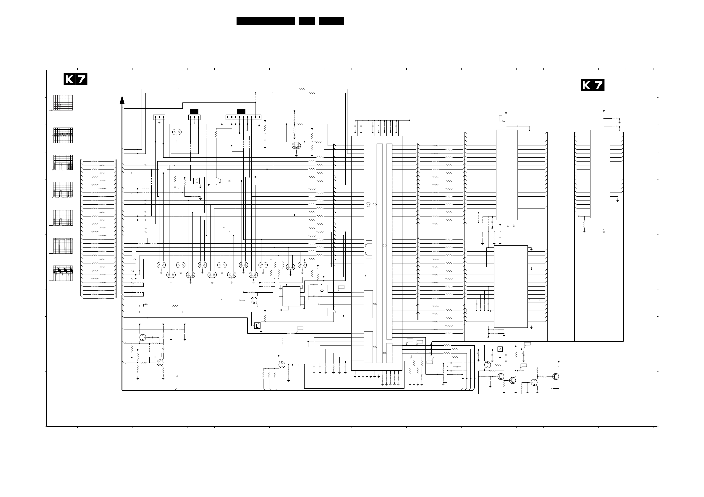
Circuit Diagrams and PWB Layouts
63F21RE AB 7.
Small Signal Board: TXT and Control
2044 K15
0341 B7
0355 B6
0356 B5
0375 F9
1001 I10
2001 L16
2002 K17
2003 G17
2013 K11
2005 B18
2006 G16
2007 F17
2008 C13
2009 C12
2010 C12
2011 C12
2012 C12
123
2025 K10
2035 L18
2026 K10
2027 C13
2028 C13
2029 K18
2030 K16
2031 B21
2032 K17
2037 J5
2038 J5
2039 K4
2040 C8
2041 L15
2042 K15
2043 K15
2014 I10
2015 J9
2016 H10 F216 L16
2021 K9
2022 K11
2023 K11
2024 J17
2054 I18
2045 G17
2046 J17
2049 B21 F224 C4
2050 I16
2051 I16
2052 I16
2053 I16
3004-B D10
3004-C D10
2055 K10
3001 C8
3004-D D10
3003-A E10
3005-A D10
3005-B D10
3003-B E10
3003-C E10
3005-C D10
3003-D A10
3005-D A10
3004-A D10
3006 B9
45
TXT & CONTROL
A
B
C
D
E
F
G
H
I
J
K
L
C1 Reset/c-7007
1V / div DC
10ms / div
C2 +3V3 DC
C3
6MHz/2016/1001
20mV / div AC
0.5µs / div
T11 R/77-7003
0.2V / div DC
1µs / div
T12 G/78-7003
0.2V / div DC
1µs / div
T13 B/79-7003
0.2V / div DC
1µs / div
T14
Fading/80-7003
0.2V / div DC
10µs / div
T16 CVBS
/5-7003
0.2V / div DC
20µs / div
TO 7003
DEBUG SOLUTION
3049-A
18
P(80) AD(8)
3049-B
10R
P(79) AD(17)
3049-C
36
P(78) AD(19)
3049-D
10R
P(77) AD(18)
3050-A
18
P(86) AD(10)
10R
3050-B
P(85) AD(6)
3050-C
36
P(84) AD(9)
3050-D
10R
P(83) AD(7)
3051-A
18
P(90) AD(12)
3051-B
10R
P(89) AD(4)
3051-C
36
P(88) AD(11)
3051-D
10R
5
P(87)
3052-A
18
P(94) AD(14)
10R
3052-B
P(93) AD(2)
3052-C
36
P(92) AD(13)
10R
3052-D
P(91) AD(3)
3053-A
18
P(98) AD(16)
3053-B
10R
7
P(97) AD(0)
3053-C
36
P(96) AD(15)
3053-D
10R
P(95) AD(1)
3054-D
10R
P(99) ROM_CSN
10R
3054-C
36
P(100) ROM_OEN
3054-A
18
P(104) DD(0)
3054-B
P(103) DD(15)
3055-A
18
P(108) DD(1)
10R
3055-B
P(107) DD(14)
3055-C
10R
36
P(106)
3055-D
10R
P(105)
3056-A
18
P(115)
10R
3056-B
P(114) DD(13)
3056-C
36
P(113) DD(9)
10R
3056-D
P(109) DD(6)
3057-A
18
P(119) DD(3)
10R
3057-B
P(118) DD(12)
3057-C
36
P(117) DD(10)
10R
3057-D
P(116) DD(5)
NOT FOR
SERVICE
K1:K6
LIGHT_SENSOR
K6-99
F223
P50_OUT
F224
P2-7
K8-151
27
10R
4
10R
27
10R
45
10R
27
10R
4
10R
27
10R
45
10R
2
10R
45
45
10R
27
10R
27
10R
45
10R
27
10R
45
10R
27
10R
45
10R
DC-PROT
K3-102
BC-PROT
K6-79
LNA P(115)
K1-126
K2-44
P2-6
K1-301
P2-5
K1-91
STANDBY
K2-40
FRONT-DETECT
AD(5)
K6-72
FBCSO
K8-170
MCS_MPEG
C5-77
P50_IN
K2-26
K3-103
SOUND-ENABLE
K3-93
RESET-AUDIO
HD_HOME
K6-104
SCAVEM_SW
K1-49
SDA-F
K6-71
K3-95
K1-48
SCL-F
K6-70
DD(8)
K3-94
DD(7)
K1:K7-303
SDA-S
DD(2)
K1:K7-302
SCL-S
K6-71
SDA-F
SDA-S
K6-108
SCL-F
K6-70
SCL-S
K6-107
HOSD_PIP
K6-510
K6-106
VFB
K5-59
VD
K8 or K5-47
CVBS-TXT-DS-OUT
+5V-STBY
P50_IN
3895
P50_OUT
I201
F226
F227
F230
K4-306
K6-108
F231
K6-107
F232
+3V3-STANDBY
7216
BC847B
+5V-STBY
10K
3261
3074
*
*
K4-307
4001
4002
4009
*
4012
*
4005
*
4019
*
*
VFB
3V
0V
3V2
*
RES
3262
47K
RES
8204 000 82671
SERVICE-PINS
SERVICE-DEFAULT
4014
*
4008
*
PLVA2650A
BAT254
6250
3260
RES
4802
2039
220p
3007 C10
3009-A E10
3009-B E10
3009-C B10
3009-D C10
3010 C10
3011 C9
3023-A L13
3
F228
4003
RES
*
0V
2
F229
4015
F225
6008
*
+5V-STBY
3259
6238
3V7
7205
BC847B
0V
3263
3023-B L13
3023-C L13
3023-D L13
3024 L13
3026 L15
3027-A F10
3027-B F10
3027-C F10
0356
1
SERVICE-MODE
*
6009
PLVA2650A
2037
27K
BAT254
220R
PLVA2650A
306610K
6004
PLVA2650A
3045
*
27K
+5V-STANDBY
5002
6u8
100n
K2-127
IO-BUS
3027-D F10
3028-A F10
3028-B F10
3028-C F10
3028-D E10
3029 K15
3030-A K15
3030-B K15
6012
+5V-STANDBY
PLVA2650A
2038
3067
FROM/TO
AV355 OF
AV5
0355
1
AUX-SUPPLY
4020
*
4K7
PDTC144ET
6002
100n
2
F222
7019
3068
10K
PLVA2650A
3030-C K15
3030-D J15
3031 G10
3032 G10
3033-A G10
3033-B G10
3033-C G10
3033-D G10
6
3
I219
6017
4010
*
+5V-STANDBY
PLVA2650A
3034 J8
3035 I8
3036-A H9
3036-B H9
3036-C H9
3036-D H9
3039 I7
3041 K17
MAINS_CLOCK
3059
1V2
7012
4V7
6001
3042 L16
3043 K17
3045 I5
3047 K11
3048-A K14
3048-B K14
3048-C K14
3048-D K14
7
0341
123456789
F221
F200
F201
STBY_LED
680R
*
4021
I223
PDTA114ET
6037
4V2
BZX284-C3V9
6019
PLVA2650A
6021
PLVA2650A
+3V3-STANDBY
3049-A D2
3049-B D2
3049-C D2
3049-D D2
3050-A D2
3050-B D2
3050-C E2
3050-D E2
FROM/TO
AV341 OF
AV7
F209
RC5
+5V-STANDBY
I200
PLVA2650A
3039
33K
3053-A F2
3051-A E2
3051-B E2
3051-C E2
3051-D E2
3052-A E2
3052-B F2
3052-C F2
3052-D F2
8 9 10 11 12 13 14 15
4011
F203
F219
F202
+8V6
IR-LED
KEYBOARD
4023
4022
*
*
F213
6006
+5V-STBY
10K
3035
0V5
6003
PLVA2650A
0V43
6023
PLVA2650A
+5V2
2V8
7010
PMBT2369
0V
+3V3-STANDBY
3053-B F2
3053-C F2
3053-D F2
3054-A G2
3054-B G2
3054-C G2
3054-D G2
3001
2040
F220
4025
4024
3034
3V2
7011
PDTC114ET
0V
I220
22K
3083
B-TXT
+3V3-STANDBY
620R
10n
3036-C
36
2k2
3036-D
45
+3V3-STANDBY
10K
BC857B
7020
22K
3084
3085
R-TXT
G-TXT
3055-A G2
3055-B G2
3055-C G2
3055-D H2
3056-A H2
3056-B H2
3056-C H2
3056-D H2
I212
2k2
2k2
3036-B
27
2k2
3036-A
18
VSS
NVM
SDA
5
4029
+5V2
22K
6025
PLVA2650A
4
M24C32
8
3082
3067 E5 6037 D7
3057-A H2
3057-B H2
3057-C I2
3057-D I2
3059 C7
3062 L18 3096-C D15
3063 F20
3066 D5
3005-D
45
470R
+8V6
10K
3006
3009-C
36
470R
4K7
3011
6013
PLVA2650A
1
0375
6026
PLVA2650A
WC_
7
SCL
6
E2
3
7008
*
E1
2
E0
1
VCC
T16
2015
100n
2021
*
100n
I221
2055
100n
100K
3075 H10
3076 H10
3068 E6
3080-A J15 3099-D F15
3069 L14
3080-B J15
3070 L17
3080-C J15
3071 K18
3072 L18
3080-D J15
3073 K17
3082 K9
3074 K4
3083 L8
3003-D
45
470R
+5V2
10K
3007
I213
3009-D
45
470R
10K
3010
3005-C
36
3005-B
470R
27
470R
3005-A
18
470R
3004-D
45
3004-C
470R
36
470R
3004-B
27
3004-A
470R
18
470R
3003-C
3
6
470R
3003-B
7
2
3003-A
470R
18
3009-B
470R
27
3009-A
470R
1
8
470R
3028-D
45
3028-C
470R
36
3028-B
470R
27
3028-A
470R
18
470R
3027-D
45
470R
3027-C
36
3027-B
470R
27
3027-A
470R
18
470R
3031
3032
330R
470R
3033-D
45
3033-C
220R
36
3033-B
220R
27
220R
3033-A
18
220R
+3V3-STANDBY
4K7
3075
F208
4K7
3076
F207
2016
33p
1001
6MHZ
HC-49/U
2014
27p
RESET
P(83)
F212
I222
2025
2023
2026
100n
100n
100n
3084 L8
3085 L9
3086 I15
3090-A H15
3090-B G15
3090-C G15
3090-D H15
3091-A H15
P(105)
P(106)
P(119)
P(118)
P(117)
P(116)
P(114)
P(113)
P(109)
P(108)
P(107)
P(104)
P(103)
P(100)
P(99)
P(98)
P(97)
P(96)
P(95)
P(92)
P(91)
P(90)
P(89)
P(88)
P(87)
P(86)
P(85)
P(93)
P(94)
P(84)
24K
3047
2022
C3
F210
220n
3091-B G15
3091-C G15
3091-D H15
3092-A H15
3092-B G15
3092-C G15
3092-D I15
3093-A H15
2013
7003
SAA5801H
P2-2|ADC0
105
P2-3|ADC1
106
P3-7|CBB
120
P3-6|TTC
119
P3-5|TTD
118
P3-4
117
P3-3
116
115
P3-2
P3-1|LED1
114
P3-0|LED0
113
P2-7|ADC5
110
P2-6|ADC4
109
P2-5|ADC3
108
P2-4|ADC2
107
P2-1|PWM1
104
P2-0|PWM0
103
P1-7|RC
100
P1-6|INT3
99
P1-5|INT2
98
P1-4|INT1
97
96
P1-3|INT0
P1-2|T2
95
P0-7
92
P0-6|CORN
91
P0-5|TxDo
90
P0-4|RxDo
89
P0-3|SDA1
88
P0-2|SCL1
87
P0-1|SDA0
86
P0-0|SCL0
85
P1-0|T0
93
P1-1|T1
94
OSCOUT
16
OSCIN
17
OSCGND
18
RESET
74
HSYNC
83
VSYNC
84
FRAME
82
CVBS0
5
CVBS0_R
4
CVBS1
7
CVBS1_R
6
IREF_DEC
1
IREF
2
REF+
3
STN|BLACK
8
220n
100n
2012
VSSA10VSSD1
3093-B H15
3093-C G15
3093-D I15
3094-A E15
3094-B I15
3094-C I15
3094-D E15
3095-A C15
100n
2011
9
19
VDDA
VDDN1
C5
C6
UC
CLOCK GENERATOR
EPG
TXT
VSSP139VSSP250VSSP3
21 76
2010
20
VDD1
AND
DISPLAY TIMING
TXT
CAPTION
USA
CLOSE
VSSD2
3095-B I15
3095-C C15
3095-D E15
3096-A C15
3096-B E15
3096-D E15
3097-A D15
100n
2009
VDDP138VDDP2
VSSD3
102
100n
49
EXTERNAL CODE AND DATA INTERFACE
112
3024
470R
3097-B E15
3097-C D15
3097-D E15
3098-A D15
3098-B D15
3098-C D15
3098-D D15
3099-A F15
100n
100n
2008
2028
VDDD275VDDD3
DISPLAY
INTERFACE
TEST112TEST213TEST314TEST4
TEST0
11
7
8
3023-B
3023-A
470R
470R
2
1
2027
101
ROM_OEn
RAM_OEn
ROM_CSn
RAM_CS
CASLn
CASHn
FADING
VIDEOn
6
3023-C
470R
3
100n
RASn
WEn
DATA
5
3023-D
470R
A10
A11
A12
A13
A14
A15
A16
A17
A18
A19
A20
A21
A22
A23
D10
D11
D12
D13
D14
D15
EAn
3099-B F15
3099-C F15
3259 J5
3260 K4
3261 K4
3262 K4
3263 K5
111
VDDP3
A1
A2
A3
A4
A5
A6
A7
A8
A9
D0
D1
D2
D3
D4
D5
D6
D7
D8
D9
R
G
B
15
4
45
47
51
53
55
57
59
61
62
60
58
56
54
52
48
46
44
63
65
64
66
67
68
36
32
28
24
23
27
31
35
34
30
26
22
25
29
33
37
40
41
43
42
69
72
71
70
73
77
78
79
80
81
AD(10)
AD(11)
AD(12)
AD(13)
AD(14)
AD(15)
AD(16)
AD(17)
AD(18)
AD(19)
AD(20)
DD(10)
DD(11)
DD(12)
DD(13)
DD(14)
DD(15)
ROM_OEN
ROM_CSN
T11
T13
45
3048-D
3895 K3
4001 H4
4002 I4
4003 I4
4005 E4
4008 G4
4009 D4
4010 C6
+3V3-STANDBY
AD(0)
AD(1)
AD(2)
AD(3)
AD(4)
AD(5)
AD(6)
AD(7)
AD(8)
AD(9)
DD(0)
DD(1)
DD(2)
DD(3)
DD(4)
DD(5)
DD(6)
DD(7)
DD(8)
36
3048-C
150R
4011 B8
4021 C7
4012 E4
4022 C8
4014 E4
4015 D5
4024 H8
4017 F16
4025 H8
4018 F16
4027 F16
4019 G4
4029 J9
4802 K4
4020 C6
3095-D
45
AD(0)
AD(1)
AD(2)
AD(3)
AD(4)
AD(5)
AD(6)
AD(7)
AD(8)
AD(9)
AD(10)
AD(11)
AD(12)
AD(13)
AD(14)
AD(15) A(15)
AD(16)
AD(17)
AD(18)
AD(19)
AD(20)
DD(0)
DD(1)
DD(2)
DD(3)
DD(4)
DD(5)
DD(6)
DD(7)
DD(8)
DD(9)DD(9)
DD(10)
DD(11)
DD(12)
DD(13)
DD(14)
DD(15)
ROM_OEN
ROM_CSN
T12
P(77)
P(78)
P(79)
P(80)
18
T14
150R
150R
3048-A
27
150R
3048-B
68R
3069
100R
3096-D
45
100R
3097-D
45
100R
3098-D
45
100R
3098-A
18
100R
3097-A
18
100R
3096-A
18
100R
3095-A
18
100R
3094-A
18
100R
3099-B
27
100R
3099-A
18
100R
3092-B
27
100R
3090-B
27
100R
3091-C
36
100R
3093-C
36
100R
3092-D
45
100R
3090-D
45
100R
3091-A
18
100R
3093-A
18
100R
3086
100R
3094-B
27
100R
3080-D
45
100R
3080-B
27
100R
+3V3-STANDBY
I210
RES
*
3095-B
27
100R
3096-B
27
100R
3097-B
27
100R
3098-B
25
100R
3098-C
36
100R
3097-C
36
100R
3096-C
36
100R
3095-C
36
100R
3099-D
45
100R
3099-C
36
100R
3093-B
27
100R
3091-B
27
100R
3090-C
36
100R
3092-C
36
100R
3093-D
4
100R
3091-D
45
100R
3090-A
18
100R
3092-A
18
100R
3094-D
45
100R
3094-C
36
100R
3080-A
1
100R
3080-C
36
100R
3030-D
45
100R
36
3030-B
27
100R
18
2044
47p
2042
470R
3029
47p
3026
5002 J5
6012 C5
6001 H7
6013 C10
6238 K5
6017 G6
6250 J44023 C8
6019 G7
7001 G17
6021 H7
7002 C17
6023 G8
7003 C11
6025 G9
7006 K16
6026 G10
7007 L18
16
A(0)
A(1)
A(2)
A(3)
A(4)
A(5)
A(6)
A(7)
A(8)
A(9)
A(10)
A(11)
A(12)
A(13)
A(14)
A(15)
A(16)
A(17)
A(18)
ROM_CS
ROM_OE
4027
4017
A(20)
D(4)
D(0) D(12)
D(3)
D(7)
D(5)
D(1)
D(2)
CASL
CASH
WE
RAS
A(6)
A(7)
A(8)
F217
F216
K6-63
B-TXT
G-TXT
K6-64
F218
82p 2050
R-TXT
2051
82p
2030
BC857B
K6-65
*
7006
2006
2052
82p
+5V-STBY
47u
3042
470K
4018
2007
*
100n
10
11
12
13
14
15
2053
16
82p
17
18
19
20
21
2024
+3V3-STANDBY
2002
3073
4K7
2001
7
5
8
3030-C
100R
3030-A
100R
6002 H6
6003 H8
6004 G5
6006 G8
6008 G5
6009 H5
ROM_OE
RAM_OE
ROM_CS
RAM_CS
CASL
CASH
2043
47p
2041
47p
A(10)
A(11)
A(12)
A(13)
A(14)
A(16)
A(17)
A(18)
A(19)
A(20)
D(10)
D(11)
D(12)
D(13)
D(14)
D(15)
A(0)
A(1)
A(2)
A(3)
A(4)
A(5)
A(6)
A(7)
A(8)
A(9)
D(0)
D(1)
D(2)
D(3)
D(4)
D(5)
D(6)
D(7)
D(8)
D(9)
RAS
WE
*
F215
K6-62
FBL-TXT
7016 L17
7008 I9
7019 D6
7009 J17
7020 K9
7010 I8
7205 K5
7011 J8
7216 J4
7012 E7
F200 B7
7013 C20
F201 B7
7014 L18
7015 L19
F202 B8
17 18 19
+3V3-STANDBY
C4
7002
22
M27V160
VCC
10
Q15A-1
A0
9
A1
8
A2
7
A3
6
A4
5
A5
4
A6
3
A7
41
A8
40
A9
39
A10
38
A11
37
A12
ROM
36
A13
35
A14
34
A15
33
A16
2
A17
1
A18
11
En
13
Gn
32
BYTEn|VPP
VSS131VSS2
12
+3V3-STANDBY
100n
2003
2045
100u
7001
100n
HYB3118165
1
VCC1
2
IO1
3
IO2
4
IO3
5
IO4
6
VCC2
7
IO5
8
IO6
9
IO7
IO8
NC1
NC2
WE_
RAS_
A11|NC
A10|NC
A0
A1
A2
A3 A4
VCC3
1n
2046
100n
7009
+3V3-STANDBY
LF33CV
IN OUT
GND
2032
100n
100n
3041
10K
7016
BC847B
F214
100n
10K
3070
F203 B7
F204 K18
F205 K18
F207 H10
F208 H10
F209 B7
F210 I11
F212 J10
2005
100n
30
14
Q0
16
Q1
18
Q2
20
Q3
23
Q4
25
Q5
27
Q6
29
Q7
15
Q8
17
Q9
19
Q10
21
Q11
24
Q12
26
Q13
28
Q14
42
A19
VSS3
IO16
IO15
IO14
IO13
RAM
VSS2
IO12
IO11
IO10
IO9
NC3
LCAS_
UCAS_
OE_
A9
A8
A7
A6
A5
VSS1
C2
F204
4K7
3043
2029
C1
F205
RESET
7007
BC847B
47K
3072
2035
*
*
F229 C5
+3V3-STANDBY
F230 F4
F231 H4
F232 H4
F233 L19
I200 D7
I201 E4
I210 L15
*
I212 B9
I213 C10
I219 C6
I220 K8
I221 K9
I222 K10
I223 C7
20 21 22
+3V3-STANDBY
2049
82p
2031
100n
23
VCC
15
D(0)
DQ0
17
D(7)
DQ1
19
D(1)
DQ2
21
D(6)
DQ3
24
D(2)
DQ4
26
D(5)
DQ5
28
D(3)
DQ6
30
D(4)
DQ7
16
DQ8
18
DQ9
20
DQ10
22
DQ11
25
D(1)
DQ12
FLASH
27
D(7)
DQ13
29
D(0)
DQ14
31
A(0)
DQ15A-1
33
BYTE_
2
RB_
1
NC
32
A(1)
A(2)
A(3)
A(4)
A(5)
A(6)
A(7)
A(8)
A(9)
A(10)
A(11)
A(12)
A(13)
A(14)
A(15)
A(16)
A(17)
A(18)
WE
RAM_CS
RAM_OE
RESET-FLASH
7013
*
M29W400T
11
A0
10
A1
9
A2
8
A3
7
A4
6
A5
5
A6
4
A7
42
A8
41
A9
40
A10
39
A11
38
A12
37
A13
36
A14
35
A15
34
A16
3
A17
43
W_
12
E_
14
G_
44
RP_
VSS113VSS2
4K7
3063
*
A
B
C
D
E
F
G
H
I
J
K
L
F221 B7
F213 D8
F222 B6
F214 L17
F223 C4
F215 L15
F225 D5
F217 L16
F226 E4
F218 L16
F227 F4
F219 B8
F220 D8
F228 C4
D(15)
D(0)
D(1)
D(2)
D(3)
D(4)
D(5)
D(6)
D(7)
D(8)
D(9)
D(10)
D(11)
D(12)
D(13)
D(14)
A(19)
42
41
D(11)
40
39
D(10)
38
D(13)
37
36
D(9)
35
D(14)
34
D(8)
33
D(15)D(6)
32
D(6)
31
CASL
30
CASH
RAM_OE
29
82p
2054
28
A(5)
27
A(4)
26
A(3)
25
A(2)
24
A(1)
23
A(0)A(9)
22
47u
*
4K7
3071
3062
47K
7014
BC847B
100n
*
*
RESET-FLASH
BC857B
7015
F233
M
CL 36532030_011.eps
1
2
34
5
678
9101112
13 14
15
16
17 18 19 20 21 22
M
030403
Page 64
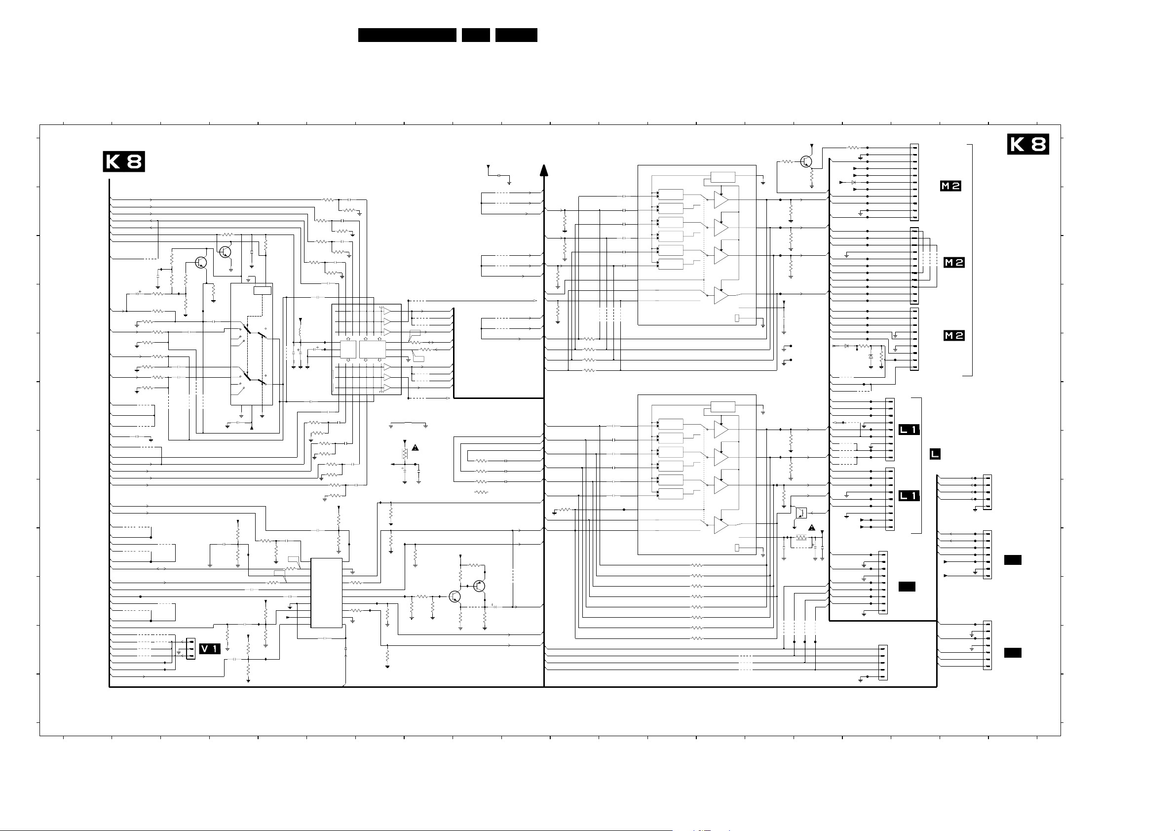
Circuit Diagrams and PWB Layouts
64F21RE AB 7.
Small Signal Board: Source Selection Add. to Diagram K1
A
0312 K3
0351 A18
0352 B18
0353 E18
0361 F17
0362 G17
0368 K17
0370 G19
0371 I19
2249 J4
0372 I17
0373 J19
2250 I4
2242 G7
2251 J9
2243 J4
2252 B12
2244 K4
2253 B12
2245 J5
2254 C12
2246 K6
2255 B12
2247 H6
2256 B12
2248 I5
2257 C12
123
2258 G8
2259 D15
2260 K6
2431 G12
2432 H12
2433 F12
2434 G12
2435 G12
2436 I16
2437 I16
2438 I15
2440 A9
2507 G10
2508 G10
2509 G10
2568 G2
2842 D2
2843 C2
SOURCE SELECTION
2852 C6
2853 F6
2854 C6
2855 G6
2856 B6
2857 G6
2858 B6
2859 H7
2860 D6
2861 F6
2862 E3
2863 D4
2864 E6
2865 C4
2867 D3
2868 E3
2870 C6
2871 F6
2872 E5
3238 K4
3278 J9
3279 J9
3281 J8
3282 K4
3283 K4
3284 H6
3285 I6
3286 J5
3287 K5
3288 I5
3289 J5
3290 G7
3291 J7
3292 H7
3293 I7
3294 J7
3295 K7
3296 I8
3239 B11
2873 E5
3251 C11
2880 F4
2893 G12
3267 C11
3214 B15
3268 D11
3217 C15
3269 J7
3226 C15
3275 I9
3234 I5
3276 I9
3237 I5
3277 J8
45
(ADDITIONAL TO K1)
K2-505
SNDR-SC4-IN
K2 OR K3-42
SNDR-SC3-IN
B
C
D
E
F
G
H
I
J
K
L
K2 OR K3-28
SNDR-SC2-IN
K2-16
IN-SC1-SNDR
K2 OR K3-13
SNDR-SC1-OUT
P2-7
K7-151
P7-2
K6-59
K6-60
K1-52
K1-51
K2-33
4614
4616
4618
NO FBX
2842
10u
2568
100p
NO FBX
NO FBX
F807
4807
3865
RES
3871
RES
3864
22K
3870
RES
4500
4212
4853
4615
4617
4619
4627
4626
4434
4435
IN-FRONT-SNDR
K2-39
IN-FRONT-SNDL
SNDL-U_I-IN
K2-41
IN-FRONT-SNDR
SNDR-U_I-IN
K1-47
CVBS-TXT-OUT
K7-47
CVBS-TXT-DS-OUT
K2-23
CVBS-SC1-IN
K1-400
N_52502
IN-FRONT-SNDL
K2 OR K3-14
SNDL-SC1-OUT
K2-17
IN-SC1-SNDL
K2 OR K3-29
SNDL-SC2-IN
K2 OR K3-43
SNDL-SC3-IN
K2-504
SNDL-SC4-IN
K1-38 or K2
FRONT-C
CVBS_Y-UI
K1-55
Y-DEC
K6-201
Y-FEAT
K6-206
U-OUT
K1-54
U-DEC
K6-202
U-FEAT
SDA-S
SCL-S
K2-35
IN-SC2-CVBS_Y
K2-1
CVBS-SC4-IN
K6-207
V-OUT
K1-53
V-DEC
K6-203
V-FEAT
C-UI
VD
HD
HA
VA
HA1
VA1
IN-C_IN-R-SC2
8204 000 81009
I825
2u2
8K2 3883
3863
RES
3869
RES
3862
6K8
3868
RES
F802
NO LTP
F803
NO LTP
F804
4613
4612
2843
4406
4407
I831
I832
6K8
3884
39K
3886
I826
2862
RES
2868
RES
RES
4735
7701
BC847B
3887
100R
56K
3885
2867
RES
RES
4734
4733
RES
FOR AP-TOP CONNECT
2250 TO SC1-C-IN
0312
1
NO FBX
2
3
NOT USED
I827
4732
TO 0312
of
3881
3873
10K
7801
BC847B
16
VDD
5K6
3888
7776
RES
2863
LL
1
RES
5
LH
HL
2
4
HH
12
LL
LH
14
15
HL
HH
11
8
2880
RES
Vdd
3298
2250
220n
3299
75R
3238
2244
220n
RES
3872
2865
RES
9
10
LSBMSB
LOGIC
H
L
3
H
13
L
VEE7VSS
6
-7V7
100K
I828
68K
2243
220n
2249
220n
Vdd
3282
100K
68K
3283
2248
3234
39R
220n
39R
3237
3288
100R
V13
3289
100R
2245
220n
Vdd
3286
100K
Vdd
I816
68K
3287
I830
3K3
3879
3K3
3877
3K3
2870
220n
2860
220n
7777
TEA6422D
+8V6
6u8
5757
I820
8V2
2864
4V
1n
100u
I821
22u
4736
2873
2872
2861
220n
2871
220n
3878
3K3
3855
10K
3880
3K3
3857
10K
2247
220n
7208
TEA6415CD-TR
V12
10
2V9
IN1
2
5V
SDA
20
3V1
IN2
4
4V9
SCL
1
2V9
IN4
5
2V9
IN6
7
0V
SUB
11
3V2
IN5
9
7V9
VCC1
3
3V1
IN3
2260
1n
3297 J8
3461 E17
3298 I4
3570-A H9
3299 I4
3570-B G9
3437 I16
3570-C G9
3448 G15
3570-D H9
3449 G15
3583 A15
3450 H15
3584 A16
3453 H11
3585 A17
3460 E17
3850 B6
67
2858
3850
3K3
220n
3860
10K
2856
220n
3858
10K
2854
220n
3856
10K
2852
220n
3854
10K
4V
4V
4V
4V
4V
0V
25R124R223R320R419R518
3VS
2CAP
SUPPLY BUS DECODER
1 GND
0V
7
8
0V
NC
21
22
4L15L26L39L410
4V
2853
220n
2855
220n
3882
3K3
3859
10K
3851
3K3
3861
10K
Vdd
3284
100K
68K
3285
8
IN7
19
GND1
13
OUT1
14
OUT2
17
OUT3
18
OUT4
15
OUT5
16
SWITCH
OUT6
12
GND2
6
IN8
2246
FRONT-Y_CVBS
R6
L511L6
4V
4V
4V
4V
4V
GND-2-SEP
2857
220n
2859
220n
I808
I829
3V1
0V
2V1
3269
0V
560R
0V
2V7
I814
0V
I815
3291
0V
560R
0V
2V9
220n
K2-509
3851 H6
3854 C6
3855 G6
3856 C6
3857 G6
3858 B6
3859 G6
3860 B6
3861 H6
Vdd
3294
3295
ROUT2
3292
3293
10K
470R
10K
470R
+8V6
3290
3862 E2
3863 D2
3864 E2
3865 D2
3866 E8
3867 E8
3868 E2
3869 D2
3870 F2
I823
13ROUT1
15
17ROUT3
4V
28SDA
27SCL
26ADDR
12LOUT1
4V
14LOUT2
16LOUT3
I824
2242
I811
3883 D3
4206 I16
4219-D E11
4406 I3
3871 E2
3884 C3
4212 F2
3872 C5
3873 B4
3885 D3
3877 C6
3886 C3
3878 F6
3887 C3
3879 C6
3888 D4
3880 G6
4006 E17
3881 B6
4202 J9
3882 G6
4203 I10
8
4750
4V
3866
100R
0V
4V
4R7
F805
10u
3297
K3-16
SNDR-SC1-IN
4728
SNDR-SC4-IN
4411
IN-SC1-SNDR
FDSR-OUT
V10
5V
SDA-S
3867
SCL-S
4V9
100R
V11
K3-17
SNDL-SC1-IN
4729
SNDL-SC4-IN
4412
IN-SC1-SNDL
FDSL-OUT
HCC-L
4751
K3-131
220n
2258
10K
3296
I813I812
3281
1V4
1K8
10K
2K2
3277
9
+8V6
3570-B
100R
3570-C
100R
3570-D
100R
3570-A
100R
Vdd
3275
33R
3276
390R
I818
6V9
7206
BC847B
4202
0V8
RES
3278
3279
330R
4215 D12
4216 D12
4217 D12
4218 D12
4219-A E11
4219-B E11
4219-C E11
I817
7V5
7207
BC857B
1V5
I819
2251
47u
150R
4222-A J14
4222-B I14
4222-C I14
4222-D J14
4400 G17
4401 G17
4402 G17
4403 G17
10
K1/K8
2440
100n
(Y-DS-2FH)
4415
4423
4416
4424
4417
4433
2507
100n
2508
100n
2509
100n
PIP-R
FEAT-Y
Y-FEAT
(U-DS-2FH)
PIP-G
FEAT-U
U-FEAT
HCC-R
(V-DS-2FH)
PIP-B
FEAT-V
V-FEAT
K2-18
IN-SC1-B
K2-20
IN-SC1-G
K2-21
IN-SC1-R
K1-602
R-SC1-IN
K1-601
G-SC1-IN
K1-600
B-SC1-IN
Y_CVBS-SC2-IN
K2 or K9 -35
SC2-C-IN
K1-32
C-7-OUT
K1-502
4203
IN-C_IN-R-SC2
K1-33
CVBS_Y-FRONT
K1-36
C-FRONT
K1-500
4407 J3
4411 D8
4412 E8
4415 B10
4416 C10
4417 D10
4421-A J14
4421-B J14
IN-UI-R
IN-UI-G
IN-UI-B
P7-2
IN-UI-FBL
K3-130
K2-33
IN-C_IN-R-SC2
K2-32
IN-SC2-G
K2-30
IN-SC2-B
K2-34
IN-SC2-FBL
VGA-R
PIP-R
VGA-G
PIP-G
VGA-B
PIP-B
VGA-FBL
PIP-FBL
YUV-SELECT-2FH
V-FEAT
Y-FEAT
U-FEAT
3267
3268
3239
3251
75R
75R
3453
1K
4421-C K14
4421-D K14
4423 B10
4424 C10
4430 C18
4431 C18
4432 C18
4433 D10
4434 K2
11
75R
75R
2
4219-B
100R
4219-C
36
100R
4219-D
45
100R
4219-A
18
100R
4435 K2
4436 F17
4500 F2
4612 K3
4613 K3
4614 H2
4615 H2
4616 I2
4617 I2
7
4618 J2
4735 F3
4853 G2
4619 J2
4736 E5
4626 K2
4737 K15
4627 K2
4742 K16
4728 D8
4743 K15
4729 E8
4745 F17
4732 F3
4750 D8
4733 F3
4751 F8
4734 F3
4807 C2
12
1FH
TDA8601T
(RGB-SWITCH)
7209
2252
220n
2255
220n
2253
220n
2256
220n
2254
220n
2257
220n
4218
4216
4215
4217
2433
100n
2893
100n
2434
100n
2431
100n
2435
100n
2432
100n
F879
2
6
3
7
4
8
5
15
14
TDA8601T
7426
2
6
3
7
4
8
5
15
14
VIDIa1
VIDIa2
VIDIb1
VIDIb2
VIDIc1
VIDIc2
SEL
FBI1
FBI2
2FH
VIDIa1
VIDIa2
VIDIb1
VIDIb2
VIDIc1
VIDIc2
SEL
FBI1
FBI2
SELECTABLE
CLAMP
SELECTABLE
CLAMP
SELECTABLE
CLAMP
SELECTABLE
CLAMP
SELECTABLE
CLAMP
SELECTABLE
CLAMP
(RGB-SWITCH)
SELECTABLE
CLAMP
SELECTABLE
CLAMP
SELECTABLE
CLAMP
SELECTABLE
CLAMP
SELECTABLE
CLAMP
SELECTABLE
CLAMP
4856 K15
4857 K15
4858 K16
4859 K15
5757 D5
6039 E17
6040 E17
6750 A17
13
7206 J9
7207 J9
7208 I6
7209 A12
7426 F12
7427 H16
7575 A16
7701 C3
7776 D4
4222-C
36
10R
4222-B
27
10R
4222-A
8
1
10R
4222-D
45
10R
4421-A
81
10R
4421-B
72
10R
4421-C
63
10R
4421-D
54
10R
14
DECODING
DECODING
7777 D6
7801 C4
F802 I2
F803 I2
F804 J2
F805 G8
F806 D15
F807 J2
F808 B15
3-STATE
3-STATE
3-STATE
3-STATE
3-STATE
3-STATE
3-STATE
3-STATE
IOCNTR
VIDOa
VIDOb
VIDOc
GND
IOCNTR
VIDOa
VIDOb
VIDOc
GND
4737
4857
4859
F809 B15
F810 C15
F811 A17
F812 A17
F813 A17
F814 A17
F815 A17
F816 B17
F817 A17
FBO
Vp
FBO
Vp
F818 A17
F827 C17
F828 C17
F829 C17
F830 D17
F831 D17
F832 D17
F836 D17
F837 D17
F838 D17
16
+8V6
7575
3584
470R
CVBS-PIP_DS
K1-507
SC2-R-IN_C-IN
K1-603
K1-604
G-SC2-IN
K1-605
B-SC2-IN
K1-606
FBL-SC2-IN
R-PIP
G-PIP
B-PIP
K6-61
FBL-PIP
(FBL-FDS)
PIP-FBL
FBL-TXT
R-TXT
G-TXT
B-TXT
4858
4742
F882
F883
+8V6
47u
2436
2437 100n
F842 E15
F844 E15
F845 E17
F846 E18
F847 E17
F848 F17
F849 F17
F850 F17
F851 G17
3585
CVBS-TXT-OUT
-7V7
+5V2
6750
+8V6
MCL4148
+33V
K7-303
SDA-S
K7-302
SCL-S
CVBS-TXT-DS-OUT
Y-D E C
U-DEC
V-DE C
HA1
VA1
Y-DS-1FH
U-DS-1FH
V-DS-1FH
FDSL-OUT
FDSR-OUT
(Y-DS-2FH)
PIP-R
(U-DS-2FH)
PIP-G
(V-DS-2FH)
PIP-B
(FBL-FDS)
PIP-FBL
K6-?
HOSD_PIP
VFB
6039
K7-VFB
MCL4148
4006
VD
YUV-SELECT-2FH
FBL-TXT
Y-DS-1FH
U-DS-1FH
V-DS-1FH
HA-FTV
4745
I822
VA1
HA1
4402
SDA-F
4401
SDA-S
4400
SCL-S
4403
SCL-F
FEAT-Y
FEAT-U
FEAT-V
HD
VD
CVBS_Y-UI
C-UI
IN-UI-R
IN-UI-G
IN-UI-B
IN-UI-FBL
47R
F819 B17
F820 B17
F821 B17
F822 B17
F823 B17
F824 C17
F825 C17
F826 C17
15
BC847B
3583
100R
16
F808
12
1K
3214
F809
11
1K
3217
F810
10
1K
3226
F806
13
Vdd
1
9
16
12
11
10
13
1
9
220n
2259
F842
F844
I804
1K
3448
I805
1K
3449
I806
1K
3450
7427
PDTC144ET
3437
I834
4R7
100n
2438
4206
4743
4856
F881
F852 F17
F853 G17
F854 G17
F855 G17
F856 G17
F857 H17
F858 H17
F859 H17
F860 H17
I833
+5V2-FB
+8V6
3460
F847
4436
F861 H17
F870 G19
F871 H19
F872 H19
F873 H19
F874 I19
F875 I19
F876 I19
F877 I19
F878 I19
0351
1
2
3
4
5
6
7
8
9
10
11
0352
1
2
3
4
5
6
7
8
9
10
11
1
2
3
4
5
6
7
8
9
0353
18
F879 H12
F880 L17
F881 K16
F882 K16
F883 K16
I804 F15
I805 G15
I806 H15
I808 H7
4430
4432
4431
FROM/TO
FBX
+5V2
+8V6
TO
0351
TO
0352
TO
0353
SNDR-U_I-IN
SNDL-U_I-IN
MCS_MPEG
SDA-S
SCL-S
F862 I17
F863 I17
F864 J17
F865 J17
F866 J17
F867 J17
F868 J19
F869 K19
17
F817
F811
F818
F812
F813
F814
F815
F819
F820
F816
F821
F822
F823
F824
F825
F826
F827
F828
F829
F830
F831
F836
F837
F838
F832
F845
10K
6040
F848
F849
F850
F852
F851
F853
F854
F855
F856
F857
F858
F859
F860
F861
F862
F863
F864
F865
F866
F867
F880
22K3461
BZM55-C3V9
0361
9
2V4
8
2V1
7
2V1
6
0V
5
0V
4
0V3
3
0V
2
4V9
1
4V8
0362
4V2
9
8
3V2
7
2V7
6
0V
5
0V8
4
0V5
3
0V
2
5V
1
8V3
0372
1
2
3
4
5
6
7
8
9
0368
1
2
3V
0V
3V
-7V8
5V6
8V3
33V
5V9
5V
0V
3V
3V4
2V7
2V7
0V
0V3
0V
2V4
2V5
2V2
4V1
4V1
0V
0V
0V
0V
0V
0V
0V8
F846
0V2
0V
TO
0361
TO
0362
FROM/TO
AV372 OF
AV7
3
NOT USED
4
5
I811 I8
I812 J8
I813 J8
I814 J7
I815 J7
I816 J5
I817 I9
I818 J9
I819 J9
19
VGA-R
VGA-G
VGA-B
VGA-FBL
HD
VD
SDA-S
SCL-S
F870
F871
F872
F873
F874
F875
F876
F877
F878
F868
F869
I820 E6
I821 E6
I822 F17
I823 D8
I824 F8
I825 C3
I826 D3
I827 D3
I828 I4
PIP FDS
0370
1
2
3
4
5
0371
1
2
3
4
5
6
7
0373
1
2
3
4
5
6
7
U-I
I829 I6
I830 K5
I831 K3
I832 K3
I833 E17
I834 I15
20
NC.
FROM/TO
AV371 OF
AV4
FROM/TO
AV373 OF
AV8
A
B
C
D
E
F
G
H
I
J
K
L
123
45
678
9
10
11121314
CL 36532030_012.eps
15
16
17
18
19
20
030403
Page 65
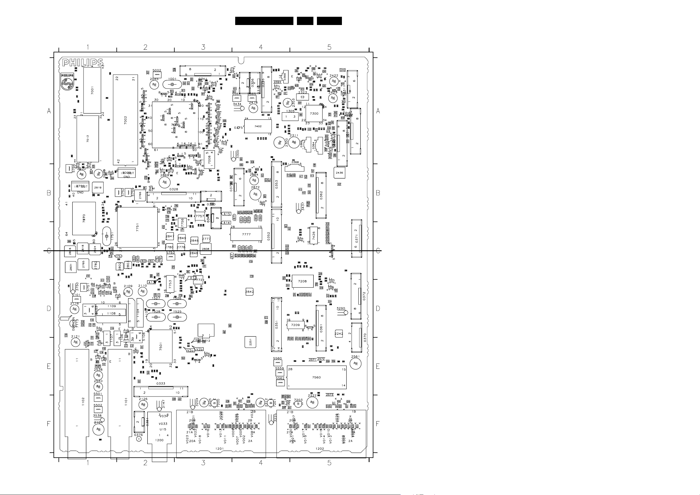
Circuit Diagrams and PWB Layouts
Layout Small Signal Board (Overview Top Side)
Part 1
CL 36532030-01a.eps
CL 36532030-01b.eps
3104 303 37046
Part 2
65F21RE AB 7.
CL 36532030_001.eps
030403
0310 A4
0311 A5
0312 D3
0315 A5
0328 B2
0333 E2
0340 A5
0341 A3
0344 C3
0348 B3
0351 D4
0352 C4
0353 B4
0355 A4
0356 A4
0360 B3
0361 D5
0362 B5
0364 A5
0366 A5
0368 B5
0369 A4
0370 E5
0371 C5
0372 D5
0373 B4
0375 A4
0376 F2
0381 F2
1001 A2
1101 F1
1102 F1
1104 D2
1105 D2
1106 D2
1107 D1
1108 D1
1109 D1
1200 F2
1201 F3
1202 F5
1305 A4
1525 D3
1526 D2
1527 D2
1528 D2
1751 C1
2001 B2
2002 B1
2003 A1
2005 A1
2006 A1
2007 A1
2008 A2
2009 A2
2010 A2
2011 A2
2012 A3
2013 A3
2014 A2
2015 A3
2016 A2
2021 A3
2022 A3
2023 A3
2024 A1
2025 A3
2026 A3
2027 A3
2028 A3
2029 B1
2030 B1
2031 A1
2032 B1
2035 B1
2037 A2
2038 A2
2039 A3
2040 A3
2041 B3
2042 B3
2043 B3
2044 B3
2045 A2
2046 B1
2049 A1
2050 A1
2051 A1
2052 A1
2053 A1
2054 A1
2055 B3
2101 F1
2109 D2
2110 D2
2116 D1
2117 E2
2119 C1
2121 D1
2126 F2
2204 F3
2205 F3
2212 F4
2213 F4
2222 F5
2224 F4
2226 F4
2240 F5
2241 F5
2242 D5
2243 D4
2244 D5
2245 D5
2246 D5
2247 D5
2248 D5
2249 C5
2250 C4
2251 D4
2252 E5
2253 E5
2254 E5
2255 E5
2256 E5
2257 E5
2258 D5
2259 E4
2260 D5
2300 A4
2301 A5
2303 A5
2304 A5
2307 A4
2308 A4
2309 A5
2310 A4
2311 A5
2312 A4
2315 A5
2321 A5
2322 A5
2323 A5
2324 A4
2325 A5
2331 A5
2340 A5
2344 A5
2351 A5
2352 A5
2406 A5
2407 A5
2408 A5
2410 A5
2411 A5
2412 A5
2413 A4
2414 A4
2415 A4
2416 A4
2417 A4
2418 A4
2422 A5
2423 A5
2424 A5
2425 A5
2426 A5
2428 A5
2429 A5
2430 A5
2431 C5
2432 C5
2433 C5
2434 C5
2435 C5
2436 B5
2437 B5
2438 C5
2440 B5
2501 E2
2502 E2
2503 E2
2504 E2
2505 E2
2506 E2
2507 E3
2508 E3
2509 E3
2510 E3
2511 E3
2512 E3
2520 D2
2521 D3
2522 D3
2525 D2
2526 D2
2527 D2
2528 D2
2533 E3
2538 E1
2539 E3
2540 E1
2541 E2
2545 E2
2550 E5
2555 F5
2556 E5
2557 E5
2558 E5
2560 E5
2561 E5
2562 E5
2565 E2
2566 E2
2568 E3
2570 E5
2571 E5
2572 E5
2573 F5
2751 C1
2753 C2
2761 C2
2762 C2
2765 C1
2766 B2
2769 B2
2770 C3
2771 C3
2772 C3
2775 B2
2776 C2
2777 C3
2778 C3
2780 C2
2782 C1
2783 B3
2784 B3
2790 C3
2791 B3
2792 B3
2801 C1
2802 C1
2803 C2
2804 C2
2805 C2
2806 C2
2807 C2
2808 C3
2810 C1
2811 B2
2813 B1
2815 C1
2816 C1
2817 B1
2818 C1
2819 B1
2820 B1
2822 B1
2824 C1
2826 D3
2827 B1
2829 C1
2831 C1
2832 C3
2833 D3
2834 C3
2837 B1
2838 C3
2839 D3
2840 C3
2841 C3
2842 D4
2844 D3
2845 C3
2846 C3
2847 C2
2848 C3
2849 C3
2851 D3
2852 C4
2853 C4
2854 C4
2855 C4
2856 B4
2857 C4
2858 B4
2859 C4
2860 B4
2864 B4
2869 B2
2870 B3
2871 C3
2872 B4
2873 C4
2893 C5
2895 C1
2897 C1
2900 C3
2901 B2
3001 A3
3003 A3
3004 A3
3005 A3
3006 A3
3007 A3
3009 A3
3010 A3
3011 A3
3023 A3
3024 A3
3026 B2
3027 A3
3028 A3
3029 B2
3030 A3
3031 A3
3032 A3
3033 A3
3034 B2
3035 B2
3036 B3
3039 B2
3041 B1
3042 B2
3043 A2
3045 A4
3047 A3
3048 A3
3049 A3
3050 A3
3051 A3
3052 A3
3053 A3
3054 A2
3055 A2
3056 A2
3057 A3
3059 A3
3062 B1
3063 A1
3066 A3
3067 A4
3068 A4
3069 A3
3070 A2
3071 B1
3072 B1
3073 A2
3074 A3
3075 A3
3076 A3
3080 B2
3082 B3
3083 B3
3084 B3
3085 B3
3086 A2
3090 A2
3091 A2
3092 A2
3093 A2
3094 A2
3095 A2
3096 A2
3097 A2
3098 A2
3099 A2
3102 E1
3107 D1
3109 D1
3110 D1
3111 D1
3112 D1
3113 D1
3114 C1
3115 D1
3116 D1
3117 D1
3121 E1
3122 D1
3123 D1
3124 D2
3135 E1
3136 D2
3137 E2
3140 D2
3141 D2
3142 C1
3143 C2
3145 E1
3146 E1
3147 F2
3148 E1
3149 D1
3154 D1
3155 D1
3204 F3
3214 D5
3217 D5
3225 F4
3226 D5
3228 E4
3229 F4
3234 D5
3237 D5
3238 C5
3239 E5
3247 F4
3248 F4
3249 F4
3251 E5
3252 F4
3253 F4
3254 F4
3255 F4
3259 A3
3260 A3
3261 A3
3262 A3
3263 A3
3264 F3
3265 F3
3266 F4
3267 E5
3268 D5
3269 C5
3270 F5
3271 F5
3273 F5
3274 F5
3275 C5
3276 D5
3277 D5
3278 D5
3279 D5
3281 D5
3282 D4
3283 D4
3284 D5
3285 D5
3286 C5
3287 C5
3288 D4
3289 D5
3290 D5
3291 C5
3292 C5
3293 C5
3294 C5
3295 C5
3296 C5
3297 C5
3298 C4
3299 C4
3300 A3
3302 A5
3303 A4
3304 A4
3307 A4
3308 A4
3309 A4
3310 A5
3311 A4
3312 A4
3313 A5
3314 A4
3315 A5
3316 A5
3317 A4
3318 A4
3320 A5
3321 A5
3322 A5
3324 A5
3325 A5
3326 A5
3330 A5
3331 A5
3332 A5
3334 A5
3340 A5
3341 A5
3342 A5
3344 A5
3345 A5
3350 A5
3351 A5
3352 A5
3353 A5
3369 A5
3370 A5
3400 A5
3401 A5
3402 A5
3404 A5
3405 A5
3406 A5
3407 A5
3408 A5
3409 A5
3412 A5
3420 A5
3423 A5
3424 A5
3425 A5
3426 A5
3427 A5
3428 A5
3429 A5
3430 A5
3431 A4
3432 A4
3433 A4
3434 A4
3435 A5
3436 A4
3437 B5
3448 C5
3449 C5
3450 C5
3453 C5
3460 B4
3461 B4
3521 D3
3530 E3
3531 E3
3538 F1
3545 E2
3546 E2
3551 E5
3552 E5
3557 E5
3558 E5
3560 E2
3565 E2
3566 E2
3569 E2
3570 E3
3583 E3
3584 E3
3585 E3
3750 C1
3751 C2
3752 C2
3753 C2
3754 C2
3755 B2
3756 B1
3758 C3
3760 C2
3761 B3
3762 C2
3765 C3
3766 C3
3767 B3
3768 B3
3780 B2
3781 C1
3782 C2
3784 C2
3785 C2
3786 C2
3787 C2
3788 C2
3789 C2
3790 C2
3791 C2
3792 C2
3793 C2
3794 C2
3795 C2
3798 D2
3799 D3
3800 D3
3801 C3
3802 B2
3811 B1
3812 B1
3813 B1
3814 C1
3818 B1
3819 B1
3820 C3
3821 C3
3822 C3
3825 D3
3827 C3
3828 D3
3829 D2
3833 B2
3837 D3
3838 B1
3839 B1
3840 B2
3841 B1
3842 C3
3844 B3
3845 B3
3846 B3
3847 B3
3848 C3
3849 D3
3850 B4
3851 C4
3852 B2
3853 B2
3854 B4
3855 C4
3856 B4
3857 C4
3858 B4
3859 C4
3860 B4
3861 C4
3866 B3
3867 B3
3873 B4
3877 B4
3878 C4
3879 B4
3880 C4
3881 B4
3882 C4
3890 C2
3891 C2
3894 D3
3895 A3
3897 C2
3898 D2
3899 C2
3999 F1
4003 B4
4005 A3
4006 B4
4008 B3
4009 A3
4010 A3
4011 A4
4012 A3
4014 A4
4015 A4
4017 A2
4018 A2
4019 A4
4021 A3
4022 A3
4023 A3
4024 B3
4025 B3
4027 A2
4029 A3
4101 D1
4102 E1
4105 D1
4108 E1
4109 E1
4111 E1
4112 D2
4201 E2
4202 D5
4212 D4
4215 E5
4216 E5
4217 E5
4218 D4
4219 D5
4222 C5
4226 F2
4227 F3
4230 F3
4311 A4
4406 B5
4407 B5
4410 A5
4413 A5
4414 A5
4415 B5
4416 B5
4417 B5
4421 C5
4423 B5
4424 B5
4426 A4
4427 A4
4429 A5
4430 C4
4431 C4
4432 C4
4433 B5
4434 E3
4435 E3
4436 A4
4500 D4
4612 C4
4613 C4
4615 B4
4617 B4
4619 B4
4626 B5
4627 B5
4702 D3
4703 D2
4704 D1
4720 C2
4721 C3
4725 B3
4726 B3
4728 C4
4729 C4
4730 D3
4737 B4
4738 D3
4739 D3
4740 D3
4741 C3
4742 A5
4743 A4
4750 D3
4751 D3
4801 D3
4802 A3
4807 D3
4810 C3
4811 C3
4853 D3
4856 A4
4857 B5
4858 A4
4859 B5
4862 B2
5002 A2
5101 D1
5103 D1
5104 D1
5106 E1
5108 D2
5109 D1
5305 A5
5306 A5
5307 A5
5501 E1
5502 F1
5540 E2
5559 E4
5560 E4
5562 E4
5564 A4
5565 A4
5751 D1
5752 B1
5753 C3
5756 B1
5759 B2
6001 A3
6004 A3
6006 A3
6009 A3
6012 A3
6013 A3
6017 A3
6019 A3
6021 A3
6023 A3
6026 B3
6037 A4
6039 B4
6040 B4
6102 D1
6103 D1
6104 D1
6106 D1
6107 D1
6200 F4
6201 F4
6202 F4
6203 F4
6204 F3
6205 F4
6206 F4
6207 F3
6208 F3
6209 F4
6210 F3
6211 F3
6212 F3
6213 F3
6214 F5
6215 F5
6216 F5
6217 F5
6218 F5
6219 F5
6220 F5
6221 F5
6222 F5
6223 F5
6224 F5
6225 F5
6226 F5
6227 F5
6228 F4
6229 F4
6230 F4
6231 F4
6232 F4
6233 F3
6238 A3
6239 F5
6240 F5
6241 F5
6242 F5
6243 F5
6244 F5
6250 A3
6259 F3
6310 A4
6311 A4
6334 A5
6340 A5
6341 A5
6344 A5
6350 A5
6354 A5
6420 A5
6422 A5
6424 A5
6429 A5
6430 A5
6751 C1
6752 C2
6753 C2
6755 B2
6756 B2
6757 C1
6759 B2
7001 A1
7002 A1
7003 A2
7006 B1
7007 A2
7008 A3
7009 B2
7010 B3
7011 B2
7012 A4
7013 A1
7014 B1
7015 B1
7016 A2
7019 A3
7020 B3
7102 D2
7103 D1
7104 D1
7105 D1
7106 E1
7107 E1
7108 D2
7109 E1
7111 E2
7113 D1
7200 F3
7201 F4
7203 F5
7204 F5
7205 A3
7206 D5
7207 C5
7208 C5
7209 D4
7216 A3
7300 A5
7341 A5
7351 A5
7402 A4
7417 A4
7418 A5
7419 A5
7420 A5
7424 A5
7426 C5
7427 C5
7438 A5
7501 D2
7502 E2
7560 E5
7575 E3
7750 B1
7751 B2
7753 C2
7756 B3
7757 B3
7770 B1
7772 D3
7773 C3
7774 B2
7777 C4
7801 B4
Page 66
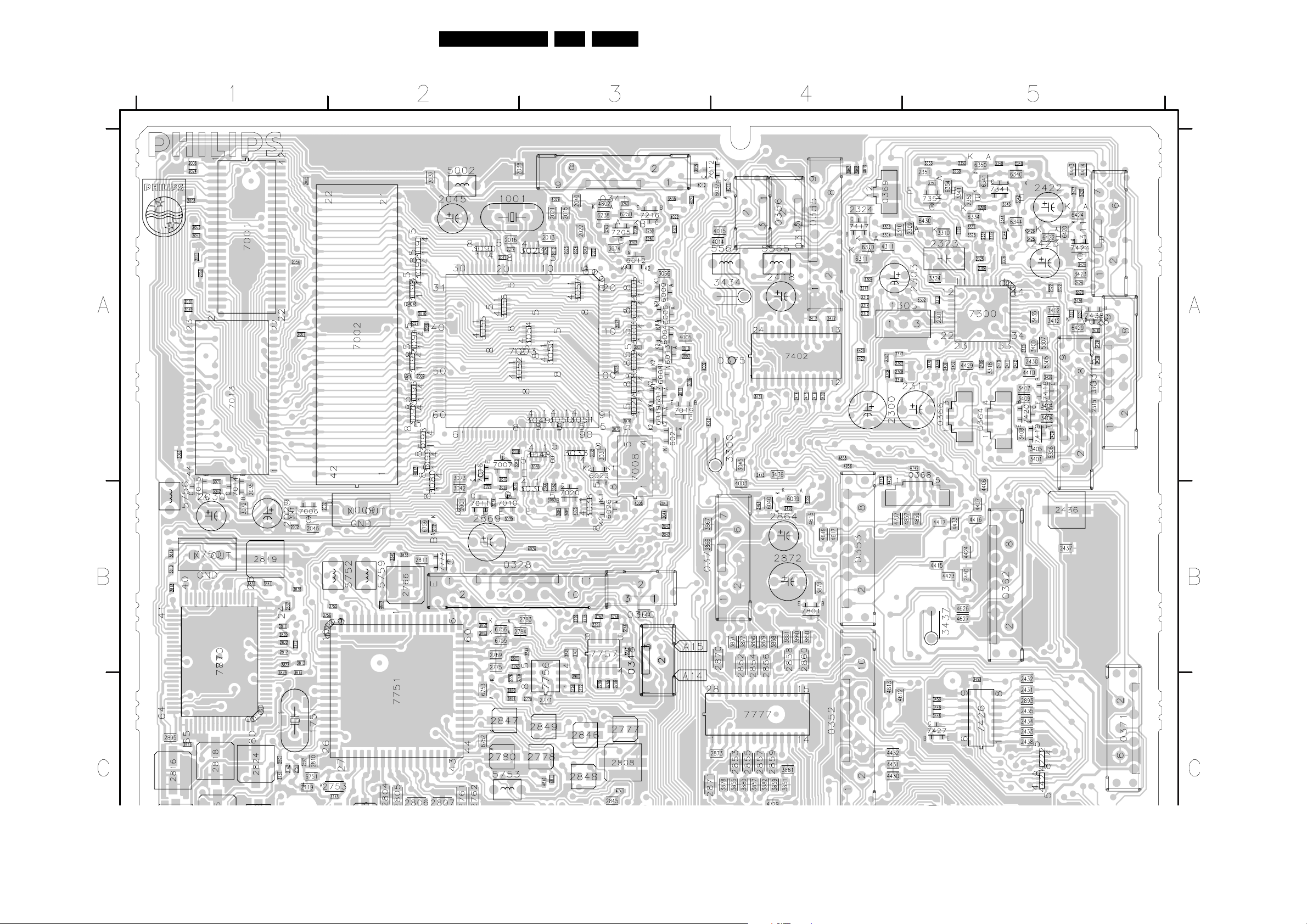
Circuit Diagrams and PWB Layouts
Layout Small Signal Board (Part 1 Top Side)
66F21RE AB 7.
CL 36532030_01a.eps
020403
Page 67
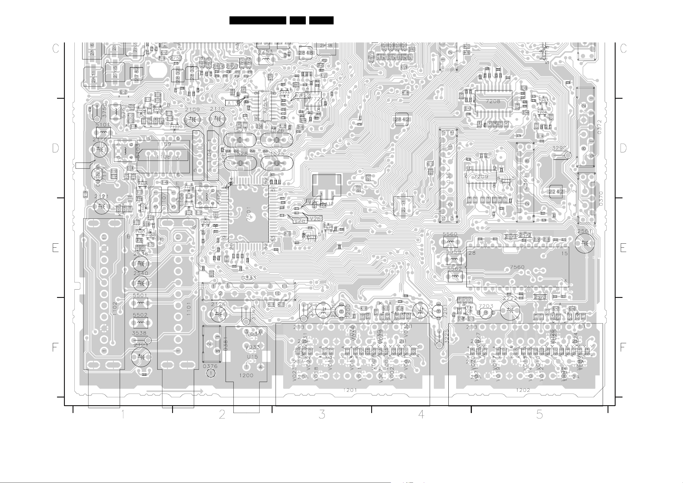
Circuit Diagrams and PWB Layouts
Layout Small Signal Board (Part 2 Top Side)
67F21RE AB 7.
CL 36532030_01b.eps
020403
Page 68
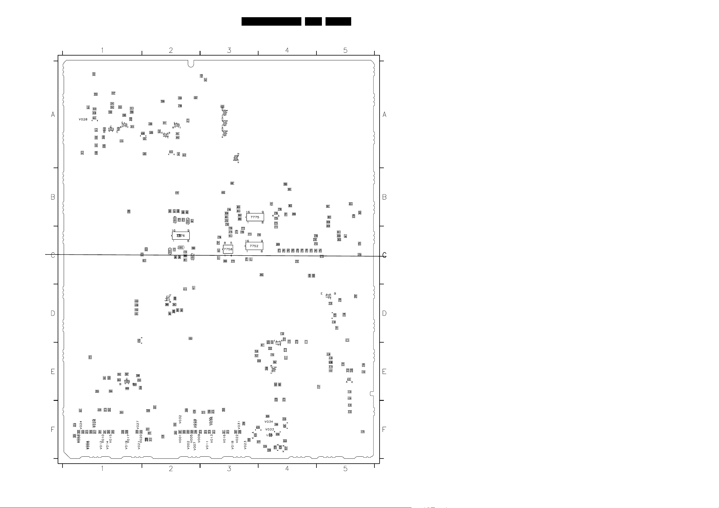
Circuit Diagrams and PWB Layouts
Layout Small Signal Board (Overview Bottom Side)
Part 2
CL 36532030_02b.eps
3104 303 37046
Part 1
CL 36532030_02a.eps
68F21RE AB 7.
CL 36532029_001.eps
030403
0310 A2
0311 A1
0315 A1
0328 B3
0333 E4
0340 A1
0341 A3
0344 B3
0348 C3
0351 D2
0352 C2
0353 B2
0355 A2
0356 A2
0360 B3
0361 D1
0362 B1
0370 E1
0371 C1
0372 D1
0373 B3
0375 A2
0376 F4
0381 F4
1001 A4
1101 E4
1102 E5
1104 D4
1105 D4
1106 E4
1107 E5
1108 D5
1109 D4
1200 F4
1201 F3
1202 F1
1305 A2
1525 D4
1526 D3
1527 D4
1528 D4
1751 C5
2029 B5
2030 B5
2045 A4
2101 F5
2102 E5
2104 E5
2105 E5
2106 D5
2107 D5
2108 D5
2109 D4
2110 D4
2111 E4
2112 C5
2116 D5
2118 D4
2120 E5
2121 D5
2122 D4
2125 F5
2126 F4
2127 E5
2202 F2
2203 F2
2205 F3
2206 F2
2209 F3
2210 F3
2212 F2
2215 F1
2216 F1
2217 F1
2218 E4
2219 F1
2220 F1
2221 F2
2222 F1
2228 F4
2229 F4
2235 F4
2300 A2
2302 A1
2303 A2
2305 A1
2306 A2
2311 A1
2313 A1
2323 A1
2343 A1
2400 A1
2401 A1
2402 A1
2403 A1
2404 A1
2405 A1
2418 A2
2419 A2
2422 A1
2423 A1
2427 A1
2441 A2
2442 A2
2532 E4
2534 D4
2535 E3
2536 E4
2537 E3
2538 E5
2540 E5
2551 E1
2552 E1
2553 E1
2554 E1
2561 E1
2564 E1
2567 E1
2569 A2
2752 C4
2754 C5
2755 C4
2756 C4
2757 C4
2758 C4
2759 C4
2760 C4
2763 C4
2764 C4
2767 C4
2768 C4
2773 C4
2774 B4
2779 C4
2781 C4
2785 B4
2786 B4
2787 D5
2788 A2
2793 B3
2797 C3
2798 C3
2799 C3
2800 C3
2809 C4
2812 C5
2814 B5
2821 B5
2823 B5
2825 B5
2828 B5
2830 C5
2835 C5
2836 C5
2843 D2
2861 C2
2862 B2
2863 C2
2864 B2
2865 B2
2867 C2
2868 B2
2869 B4
2872 B2
2880 C2
2890 B4
2891 B4
2892 C4
2898 B4
3103 F5
3104 F5
3106 D5
3118 E4
3119 E5
3133 E5
3134 D5
3138 E5
3139 E5
3147 F4
3152 E4
3153 D4
3200 F2
3201 F2
3202 F2
3203 F2
3204 F3
3205 F3
3206 F3
3207 F3
3208 F2
3209 F3
3210 F3
3211 F3
3212 F2
3213 F3
3215 F3
3216 F3
3218 F3
3219 F3
3220 F2
3221 F1
3222 F1
3223 F1
3224 F1
3225 F2
3227 F2
3230 F1
3231 F2
3232 F1
3233 F4
3235 F1
3236 F1
3240 F1
3241 F1
3242 F1
3243 F1
3244 F1
3245 F1
3246 F1
3250 F2
3256 F3
3257 F4
3258 F4
3272 F4
3280 F4
3290 D1
3300 A3
3306 A1
3323 A1
3343 A1
3413 A1
3414 A1
3421 A3
3422 A1
3434 A3
3437 B1
3438 A1
3439 A1
3440 A1
3441 A1
3442 A2
3443 A2
3444 A1
3451 A2
3452 A2
3454 A1
3532 D4
3538 F5
3553 E1
3554 E1
3556 E1
3567 E4
3568 E4
3571 E4
3590 E1
3750 D5
3769 C3
3770 C3
3771 C3
3772 C3
3773 C3
3776 C3
3777 C3
3778 C3
3779 C3
3783 C4
3796 B3
3797 B3
3817 C5
3823 B3
3824 B3
3826 F4
3830 B3
3831 B3
3832 B4
3862 B2
3863 C2
3864 B2
3865 C2
3868 B2
3869 C2
3870 B2
3871 C2
3872 B2
3883 D2
3884 D2
3885 D2
3886 D2
3887 D2
3888 D2
3892 B3
3893 B3
4001 B3
4002 B3
4020 A3
4103 D4
4104 E5
4107 E5
4110 E5
4113 D4
4114 D5
4203 D2
4206 B1
4207 A2
4208 A2
4228 E4
4229 F2
4235 F2
4316 A1
4400 D1
4401 D1
4402 D1
4403 D1
4411 D2
4412 D2
4420 A1
4425 A3
4614 C2
4616 C2
4618 C2
4700 B4
4701 B4
4732 C2
4733 B2
4734 C2
4735 B2
4736 C2
4745 E1
4803 E4
4804 E4
4805 C4
4806 C4
4809 E1
4812 C3
4813 C3
5002 A4
5101 D5
5102 E5
5103 D5
5105 E5
5108 E4
5300 A2
5301 A2
5302 A2
5501 F5
5502 F5
5553 E1
5559 E2
5560 E2
5562 E2
5564 A2
5565 A2
5751 D5
5752 B4
5753 C4
5754 C5
5755 C5
5756 B5
5757 B2
5758 B5
5759 B4
6002 A3
6003 A3
6008 A3
6025 A3
6101 E5
6105 D5
6234 F3
6235 F3
6236 F4
6237 F4
6260 F4
6261 F4
6300 A2
6431 A1
6432 A2
6750 D1
6754 B4
7002 A4
7008 A3
7009 B4
7101 D5
7112 D4
7113 D5
7200 F3
7201 F2
7203 F1
7403 A1
7425 A1
7430 A2
7431 A2
7555 E1
7560 E1
7561 E4
7701 D2
7750 B5
7752 C3
7758 C3
7775 B3
7776 C2
Page 69
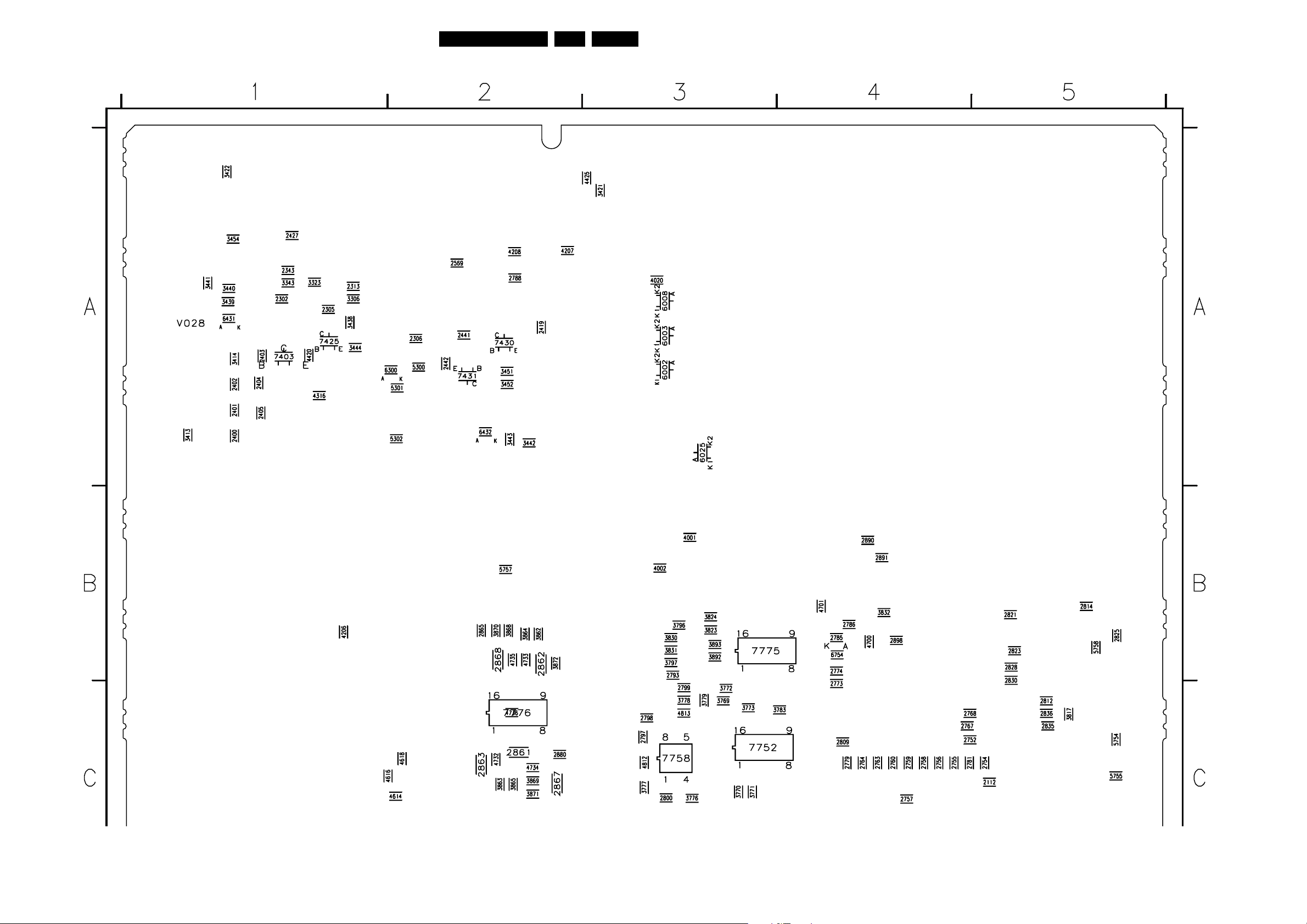
Circuit Diagrams and PWB Layouts
Layout Small Signal Board (Part 1 Bottom Side)
69F21RE AB 7.
CL 36532030_02a.eps
020403
Page 70
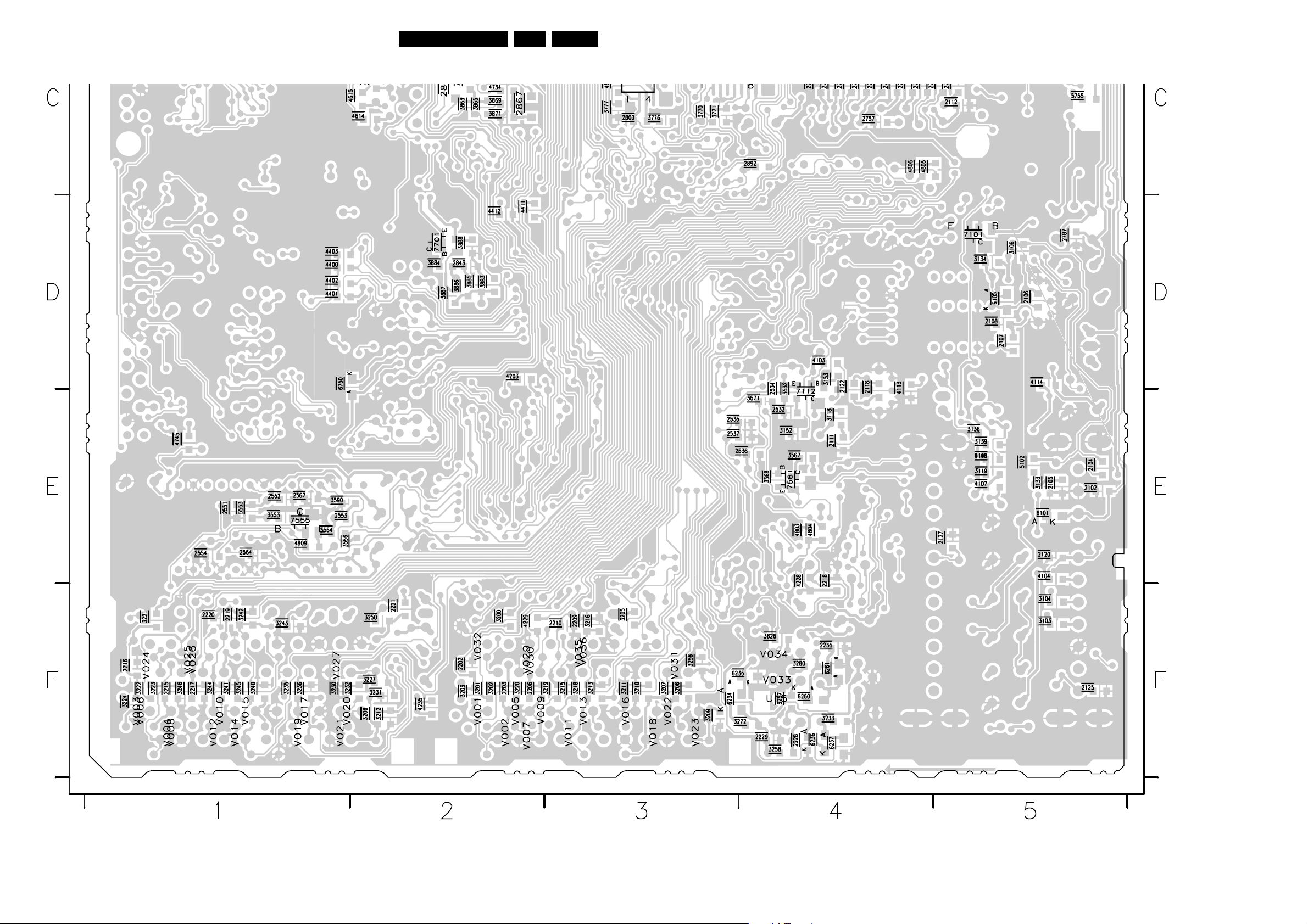
Circuit Diagrams and PWB Layouts
Layout Small Signal Board (Part 2 Bottom Side)
70F21RE AB 7.
CL 36532030_02b.eps
020403
Page 71
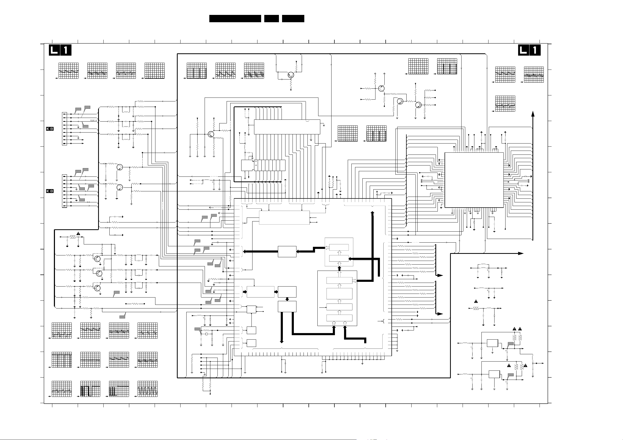
Feature Box 7 Panel: Feature Box
123456789101112131415
FEATURE BOX (FEATURE BOX 7)
A
B
C
D
E
F
G
H
I
J
K
L
M
N
FROM/TO
0362 OF
FROM/TO
0361 OF
+8V6
Y-DS-1FH
U-DS-1FH
V-DS-1FH
HA
VA
L8
500mV / div DC
20µs / div
L12
500mV / div DC
10µs / div
L16
1 V / div DC
10µs / div
L1
1 V / div DC
20µs / div
0362
4V2
3V3
2V7
0V
0V8
0V5
0V
5V
8V3
0361
2V4
2V4
2V1
0V
0V
0V3
0V
4V9
4V8
F100
9
F101
8
F102
7
F103
6
F104
5
F105
4
F106
3
F107
2
F141
1
F108
9
F109
8
F110
7
F111
6
F112
5
F113
4
F119
3
F114
2
F115
1
3711
2715
100n
3713
180R
3714
180R
3715
180R
L14
L1
10R
2716
2718 15p
15p
2719
15p2720
3725
100p
2721
2722
100p
L9
L13
200mV / div DC
L17
L2
1 V / div DC
L15
FEAT-Y
FEAT-U
L16
+5V2-FB
+8V6
L2
Y-DS-1FH
U-DS-1FH
V-DS-1FH
L4
L3
L5
F154
100n
3719
220R
100K
BC857B
3716
3720
220R
BC857B
3717 100K
3721
220R
100K3718
3727
150R
3K3
3863
680R
3726
1 V / div DC
10µs / div
5ms / div
1 V / div DC
100µs / div
20µs / div
HD
VD
VA
HA
SDA
SCL
4727
7700
4728
7701
4729
3728
150R
1K2
FEAT-Y
FEAT-U
FEAT-V
HD
VD
SCL
SDA
3722
7702
BC857B
56p
2723
56p
2724
680R
3723
3700
68R
3701
68R
3702
68R
3729
68R
3730
68R
2714 22p
680R
3724
L10
1 V / div DC
L14
1 V / div DC
L18
1 V / div DC
100µs / div
L3
1 V / div DC
20µs / div
2701
F121
2704
2707
F120
PMBT2369
PMBT2369
22p2713
3709
100R
3710
100R
1u2717
3740
220R
3741
220R
680R
3742
220R
L22
10µs / div
10µs / div
10p
10p
2706
10p
L23
123
Circuit Diagrams and PWB Layouts
7703
7704
5700
2u2
5701
2u2
5702
2u2
2731
2732
2733
F117
L4
1 V / div DC
10ms / div
3703
330R
2p72700
3706
390R
12p
2702
3704
330R
2p72703
3707
390R
12p
2705
3705
330R
2p7
3731
3732
47p
3743
47p
3744
47p
3745
2708
4K7
3733
4K7
3735
4K7
4K7
680R
680R
680R
3999
1K
3708
390R
12p
F217
F218
4K7
3734
5707 6u8
2734
18p
5708
6u8
2735
18p
5709
6u8
2736
18p
F159
4725
2737
150p
2738
150p
150p
2739
F116
Y_EAGLE_E
F157
U_EAGLE_E
F158
V_EAGLE_E
HD_E
VD_E
4726
SCL-D SCL-D
SDA-D
2740
F162
22n
2741
F163
22n
2742
F164
22n
L11
1 V / div DC
10µs / div
L15
1 V / div DC
10µs / div
L19
500mV / div DC
50ns / div
8204 000 64316
4 5 6 7 8 9 10 11 12 13 14 15
L5
1 V / div DC
20µs / div
+2.5VB
3788
3787
2871
100n
MF(18)
SN-DA
SN-CL
SDA-D
RSTW
RSTR_P
VAP
+5VA
+3.3VA
+3.3VA
HREF_EXT
4735
4734
L9
L11
5714
L19
F123
1K
3784
F124
F125
F126
F127
71F21RE AB 7.
4708-A J14
16 17 18 19
7728
BC847B
3791
DA(15)
DA(14)
DA(13)
DA(12)
DA(11)
DA(10)
DA(09)
DA(08)
DA(07)
DA(06)
DA(05)
DA(04)
DA(03)
DA(02)
DA(01)
DA(00)
F148
F149
F150
4710-A
18
10R
4710-B
27
10R
4709-A
18
10R
4709-B
27
10R
2763
100n
4708-A
18
4708-B
10R
27
10R
4707-A
18
10R
4707-B
27
10R
3763
22R
100n
2762
L22
500mV / div DC
5ms / div
+3.3VA
3K9
3793
7729
3792
BC847B
1K
DA(15)
DA(14)
DA(13)
DA(12)
DA(11)
DA(10)
DA(09)
DA(08)
+3.3VFM
+3.3VFM
+3.3VFM
+3.3VFM
DA(07)
DA(06)
DA(05)
DA(04)
DA(03)
DA(02)
DA(01)
DA(00)
4711
4710-C
36
4710-D
10R
45
10R
4709-C
36
4709-D
10R
45
10R
+3.3P
4708-C
36
10R
4708-D
45
10R
4707-C
36
4707-D
10R
45
10R
F139
F140
+3.3P
ALE
16
VSS
A15
2
1K
10R
3764
F151
139
137
136
138
ALE
EAN
PSEN
VSSD4
BACK END
PEAKING
MID END
HISTOGRAM
REDUCTION
TIMING
TBC/SRC
VSSO2
WE-A66WE-B
VSSD1
VDDD1
62
65
63
64
2761
100n
+3.3P
L22
500mV / div DC
5ms / div
+3.3P
+3.3P
intern
3765
100n
133
135
134
VSSD3
VSSO5
VDDD4
MUX
NOISE
MUX
2765
UVC0
4K7
3865
+1.5VC
+2.5VB
3853
8K2
15K
3797
+3.3VA
BC847B
7736
3854
3855
1K
3K9
100R
L23
1 V / div DC
20µs / div
+3.3P
2764100n
122
121
132
131
130
129
128
UVC1
UVC2
UVC3
UVC4
UVC5
127 126
BUS B
UVC6
YB074YB173YB272YB371YB470YB569YB668YB767YB8
123
125
124
YC0
YC1
UVC7
UVC8
VDDO2
BUS C
BUS D
75
120
YC2
119
YC3
118
YC4
117
YC5
116
YC6
115
YC7
114
YC8
113
WE-C
112
IE-C
111
VSSO4
110
RE-D
YD8
109
108
YD7
107
YD6
106
YD5
105
YD4
104
YD3
103
YD2
102
YD1
101
YD0
100
VDDD3
99
UVD8
UVD7
98
97
UVD6
96
UVD5
UVD4
95
94
UVD3
93
UVD2
UVD1
92
91
UVD0
90
VSSD2
89
CLK32
CLK
88
CLK16
VDDD2
87
86
VSSO3
85
CLK-AS
84
UVB0
83
UVB1
82
UVB2
UVB3
81
UVB479UVB578UVB677UVB776UVB8
80
7741
PMBT2369
3862
+5VA
2766
147
P2-0
100n
3861
10K
A10
24
146
P2-1
RSTR
+3.3VA
3K3
17
1
A1127A12
3
30
145
144 143
P2-2
P2-3
P2-4
P2
YA458YA559YA660YA761YA8
57
12
A1331A14
P2-5
26
NC
E_
G_
23
25
142
141
140
P2-6
P2-7
CLK
TIMING
L6
500mV / div DC
20µs / div
+3.3VA
4K7
3789
220K
7727
BC847B
82K
2872
100n
5712
L17
L10
L6
L8
F165
F166
4u7
2754
3760
1701
HC-49/U
12M
18p
2758
F122
47K
3872
3752
1R
3753
1R
3790
100R
4702
4u7
2748
100n
2747
F128
4701
F129
L18
F155
F156
F229
2751
100n
L13
L12
F160
F161
2757
3759
22n
220R
F118
2752
100n
2753
100n
L7
2756
100n
2755
F167
1M
18p
2759
4704
TD0MA
TRST
47K
3864
+3.3P
4700
4K73758
100n
TMS
7713
SAA4978H
1
SN-DA
2
SN-CL
3
VSSO6
4
SCL
5
SDA
6
UP-RST
7
WD-RST
8
RSTW
9
RSTR
10
FBL
11
VDDA1
12
Y-OUT
13
VSSA1
14
U-OUT
15
V-OUT
16
VSSA2
17
BGEXT
18
H-D
19
V-D
AGND
20
21
DIFFIN
VDDA2
22
Y-IN
23
24
VDDA3
25
U-IN
VIN
26
27
VSSA3
28
H-A
29
V-A
HREF-EXT
30
31
VDDA4
32
VSSA4
33
VSSX
34
OSC-I
35
OSC-O
36
TEST
TRST
37
TMS
38
39
TDI
40
TDO
F152
TD0
L7
500mV / div DC
+5VA
+5VA
+3.3VA
4733
4732
5711
20
Vcc
EN
7712
74HC573D
1
159T0160
T1TCK
VSSO1
42
41
TCK
20µs / div
+3.3VA
AD(00)
AD(01)
AD(02)
AD(03)
13Q014
15
18Q319Q420Q521Q622
Q1
Q2
VCC
7711
A2
A010A1
9
8
11
1D
219
318
417
516
AD(00)
AD(01)
AD(02)
AD(00)
AD(01)
AD(02)
155
154
156
P0-1
P0-2
P0-3
P0-0
AD(04)
A37A4
615
AD(03)
AD(04)
AD(03)
AD(04)
153
152
P0-4
P0
4731
4730
5710
32
2745
100n
M27C512
2746
100n
10
GND
C1
11
ALE
INT0
INT1
157
158
INT0
INT1
MICRO-PROCESSOR
PICNIC
ANALOG
PROCESSING
CLK
PLL
TIMING
OSC
BST
UVA0
UVA145UVA246UVA347UVA448UVA549UVA650UVA751UVA8
43 44
RSTR_P
2929
68p
AD(05)
AD(06)
AD(07)
Q7
PROM
A5
A6
A7
6
5
4
29
LATCH
714
813
912
AD(05)
AD(06)
AD(07)
100n
AD(05)
AD(06)
AD(07)
151
150
149
P0-5
P0-6
P0-7
VDDO3
PSP
3 X DAC
3 X ADC
FRONT
END
BUS A
YA054YA155YA256YA3
VDDO1
52
2760
+3.3P
A828A9
148
53
L23
1 V / div DC
20µs / div
3798
+3.3VA
18K
3796
+2.5VD
12K
3795
+3.3VC
18K
2K2
3794
7714
MS81V04160
1
2
3
4
5
6
7
8
YF(7)
YF(6)
YF(5)
YF(4)
YF(3)
YF(2)
YF(1)
YF(0)
UVF(7)
UVF(6)
UVF(5)
UVF(4)
UVF(3)
UVF(2)
UVF(1)
UVF(0)
9
10
11
12
13
CL16
14
15
16
2900
17
18
100n
19
20
21
22
23
24
25
L2
L3
100n
2769
RSTW
+3.3VFM
93
97
96
94
100
95
IE2
DI2098DI2199DI22
WE2
NC17
VSS20
VSS19
NC1
DI23
VSS1
DI24
DI25
DI26
DI27
NC2
VSS2
VSS3
VCC1
VCC2
SWCK
VCC3
VCC4
VSS4
VSS5
NC3
DI17
DI16
DI15
DI14
VSS6
DI13
NC4
RSTW2
FIELD
MEMORY 1
RSTW1
VSS735VSS839VSS9
WE1
VCC537VCC643VCC7
NC5
26
RE_F
NC638NC7
IE1
DI1028DI1127DI12
30
33
32
34
31
29
+3.3VFM
RSTW
+5V2-FB
+3.3VA
+8V6
L2
CLK32P
CL16
5705
+5VA
2725
5V
5706
+5VA
2728
91
36
2773
+3.3VFM
5V
+3.3VFM
89
VSS18
VCC1392VCC14
NC847NC946OE1
100n
2709
3857
10R
10u
10u
87
40
5713
RSTR
L24
L26
+3.3VFM
+3.3VFM
2781
100n
83
78
80
81
82
84
85
RE2
OE2
NC1386NC1488NC1590NC16
VSS16
VSS17
VCC12
RSTR2
MODE1
VSS1049VSS11
RE1
RSTR1
MODE242MODE3
100n
2726
2729
NC10
48
45
44
41
100n
+3.3VFM
+3.3VFM
RSTR
5703
5704
F153
470u
2710
2750
2749
100u
F201
5731
100n
2923
2924
LD1117
3
7705
IN2OUT
GND
1
100n
LD1117
32
7706
IN
OUT
GND
1
100n
1 V / div DC
10µs / div
1 V / div DC
10µs / div
+3.3VFM
2779
77
76
NC1179NC12
75
VCC11
74
DO20
73
DO21
72
VSS15
71
DO22
70
DO23
69
DO24
68
DO25
67
VSS14
66
DO26
65
DO27
64
VCC10
63
SRCK
62
VCC9
61
DO17
60
DO16
59
VSS13
58
DO15
57
DO14
56
DO13
55
DO12
54
VSS12
53
DO11
52
DO10
51
VCC8
50
2775
+3.3VFM
470p
2712
+3.3P
100n
+8.6VF
100n
F146
2727
F147
2730
100n
CLK32
2777
100n
+5VA
22R3809
3737 22R
L20
100u
22R3739
3810 22R
L21
100u
CL 36532021_010.eps
L25
1 V / div DC
10µs / div
MF(18)
MF(01)
MF(02)
MF(03)
MF(04)
MF(06)
MF(07)
MF(08)
MF(09)
100n2778
+3.3VFM
+3.3VFM
MF(10)
MF(11)
MF(12)
MF(13)
MF(14)
MF(15)
MF(16)
MF(17)
MF(18)
L2
L3
3V3
+3.3VA
2V5
+2.5VB
L3
F209
+3.3VFM
100n
2767 5715
040403
16 17 18 19
0361 E1
4708-B J14
0362 C1
4708-C J15
1701 L7
4708-D J15
2700 C3
4709-A I14
2701 C3
4709-B I14
2702 C4
4709-C I15
2703 C3
4709-D I15
2704 D3
4710-A H14
2705 D4
A
B
C
D
E
F
G
H
I
J
K
L
M
N
2706 D3
2707 D3
2708 D4
2709 I17
2710 I17
2712 I18
2713 G3
2714 H3
2715 H1
2716 H1
2717 I3
2718 I1
2719 J1
2720 J1
2721 K1
2722 K1
2723 F3
2724 F3
2725 L17
2726 L17
2727 M18
2728 N17
2729 N17
2730 N18
2731 I3
2732 I3
2733 J3
2734 I4
2735 I4
2736 J4
2737 I4
2738 I4
2739 J4
2740 I4
2741 I4
2742 J4
2745 D8
2746 E8
2747 F7
2748 F7
2749 J17
2750 J18
2751 H7
2752 J7
2753 J7
2754 K6
2755 K7
2756 K7
2757 I7
2758 L6
2759 L7
2760 M10
2761 M11
2762 L14
2763 I14
2764 F13
2765 F12
2766 F10
2767 M19
2769 F15
2773 G17
2775 H18
2777 F19
2778 F19
2779 D18
2781 D17
2871 E6
2872 E6
2900 F15
2923 K17
2924 K18
2929 B9
3700 C3
3701 C3
3702 D3
3703 C4
3704 C4
3705 D4
3706 C4
3707 C4
3708 D4
3709 G3
3710 H3
3711 H1
3713 I1
3714 I1
3715 J1
3716 I2
3717 J2
3718 J2
3719 I2
3720 I2
3721 J2
3722 I2
3723 I2
3724 J3
3725 K2
3726 K2
3727 J2
3728 K2
3729 E3
3730 F3
3731 F3
3732 F4
3733 E4
3734 F4
3735 F4
3737 L18
3739 M18
3740 I3
3741 I3
3742 J3
3743 I4
3744 I4
3745 J4
3752 D7
3753 D7
3758 G7
3759 I7
3760 L7
3763 K14
3764 F11
3765 F11
3784 M6
3787 E6
3788 D6
3789 D7
3790 E7
3791 C14
3792 C14
3793 B15
3794 C15
3795 C15
3796 C15
3797 C13
3798 B15
3809 L19
3810 M19
3853 B13
3854 C13
3855 B14
3857 K17
3861 A10
3862 B10
3863 K2
3864 N7
3865 B13
3872 N6
3999 M2
4700 D7
4701 G7
4702 F7
4704 L7
4707-A J14
4707-B J14
4707-C K15
4707-D K15
4710-B H14
4710-C I15
4710-D I15
4711 H15
4725 E4
4726 G5
4727 I2
4728 I2
4729 J2
4730 C8
4731 C8
4732 D8
4733 D8
4734 F6
4735 F6
5700 C3
5701 D3
5702 D3
5703 I17
5704 I17
5705 L17
5706 M17
5707 I4
5708 I4
5709 J4
5710 D8
5711 E8
5712 F7
5713 J17
5714 K6
5715 M19
5731 K18
7700 I2
7701 J2
7702 J2
7703 E3
7704 F3
7705 L18
7706 M18
7711 D9
7712 E8
7713 F8
7714 E16
7727 D6
7728 C14
7729 C15
7736 B13
7741 A10
F100 C1
F101 C1
F102 C1
F103 D1
F104 D1
F105 D1
F106 D1
F107 D1
F108 F1
F109 F1
F110 F1
F111 F1
F112 F1
F113 F1
F114 G1
F115 G1
F116 M2
F117 M1
F118 J7
F119 F1
F120 D3
F121 C3
F122 M6
F123 M6
F124 M6
F125 M6
F126 M6
F127 M6
F128 G7
F129 G7
F139 K15
F140 K15
F141 D1
F146 L18
F147 N18
F148 H14
F149 H14
F150 H14
F151 F11
F152 M8
F153 I18
F154 H2
F155 H7
F156 H7
F157 C5
F158 C4
F159 D4
F160 I7
F161 I7
F162 I5
F163 I5
F164 J5
F165 K6
F166 K6
F167 L7
F201 K18
F209 M19
F217 E4
F218 F4
F229 H7
Page 72
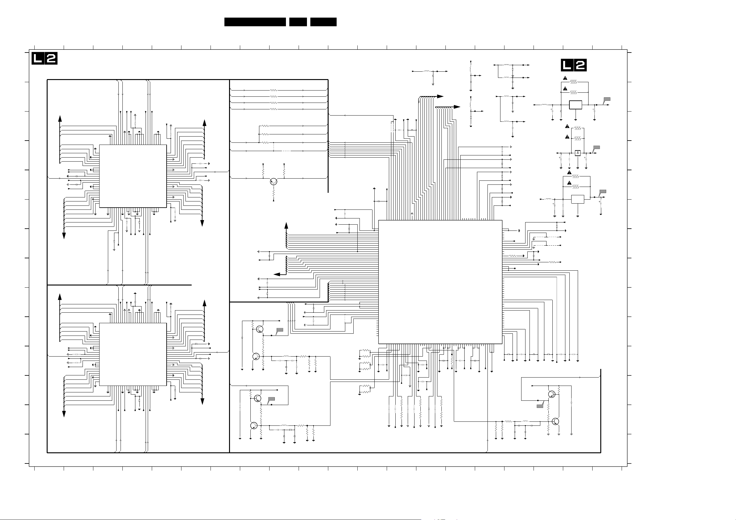
Circuit Diagrams and PWB Layouts
72F21RE AB 7.
Feature Box 7 Panel: Eagle
1234
EAGLE (FEATURE BOX 7) (ONLY PRESENT IN PIXEL-PLUS SETS)
A
B
L3
C
D
E
F
G
H
I
J
K
L
M
N
UVG(0)
UVG(1)
UVG(2)
CLK32FM5
UVG(3)
UVG(4)
UVG(5)
UVG(6)
UVG(7)
+3.3FC1
+3.3FC1
+3.3FC1
+3.3FC1
YG(0)
YG(1)
YG(2)
YG(3)
YG(4)
YG(5)
YG(7)
YG(6)
2817 100n
2884
100n
MS81V04160
1
2
3
4
5
6
7
8
9
10
11
12
13
14
15
16
17
18
19
20
21
22
23
24
25
L3
L1
UVF(0)
UVF(1)
UVF(2)
CLK32FM4
UVF(3)
UVF(4)
UVF(5)
UVF(6)
UVF(7)
+3.3FC2
+3.3FC2
+3.3FC2
+3.3FC2
L1
L3
YF(0)
YF(1)
YF(2)
YF(4)
YF(3)
YF(5)
YF(7)
YF(6)
2885
100n
MS81V04160
1
2
3
4
5
6
7
8
9
10
100n2843
11
12
13
14
15
16
17
18
19
20
21
22
23
24
25
8204 000 64316
1234567891011
RSTW_YUV
+3.3FC1
+3.3FC1
+3.3FC1
7722
100
NC17
NC1
DI23
VSS1
DI24
DI25
DI26
DI27
NC2
VSS2
VSS3
VCC1
MEMORY 5
VCC2
SWCK
VCC3
VCC4
VSS4
VSS5
NC3
DI17
DI16
DI15
DI14
VSS6
DI13
NC4
NC5
26
2820
RSTW_YUV
7723
100
NC17
NC1
DI23
VSS1
DI24
DI25
DI26
DI27
NC2
VSS2
VSS3
VCC1
MEMORY 4
VCC2
SWCK
VCC3
VCC4
VSS4
VSS5
NC3
DI17
DI16
DI15
DI14
VSS6
DI13
NC4
NC5
26
27
97
96
95
99
IE2
DI2098DI21
DI22
RSTW2
FIELD
RSTW1
WE1
IE1
DI1028DI1127DI12
30
32
31
29
100n
+3.3FC1
WEYUV_G WEYUV_G
WEYUV_F
RSTW_YUV
+3.3FC2
99
96
95
IE2
DI2097DI2198DI22
RSTW2
FIELD
WE1
RSTW1
IE1
DI1029DI1128DI12
32
30
31
+3.3FC2
RSTW_YUV
WEYUV_F
91
93
94
WE2
VSS19
VSS20
VSS735VSS839VSS9
VCC537VCC643VCC7
NC638NC740NC847NC946OE1
33
34
36
100n
2821
+3.3FC1
+3.3FC2
93
91
92
94
WE2
VSS20
VSS19
VSS733VSS835VSS9
VCC534VCC637VCC7
NC636NC738NC840NC947OE1
+3.3FC2
+3.3FC2
90
7735 L18
5 6 7 8 9 10 11 12 13 14 15 16 17 18 19 20
+3.3VC
F214
5736
+3.3VC
REUV
RSTRUV
+3.3FC1
+3.3FC1
YG0(0)
YF0(0)
UVG0(0)
UVG0(1)
UVG0(2)
UVG0(3)
UVG0(4)
UVG0(5)
UVG0(6)
UVG0(7)
YG0(1)
YG0(2)
YG0(3)
YG0(4)
YG0(5)
YG0(6)
YG0(7)
UVF0(0)
UVF0(1)
UVF0(2)
UVF0(3)
UVF0(4)
UVF0(5)
UVF0(6)
UVF0(7)
2833
100n
YF0(1)
YF0(2)
YF0(3)
YF0(4)
YF0(5)
YF0(6)
YF0(7)
L1
UVG0(0:7)
2845
100n
+3.3FC1
+3.3FC1
2846
100n
YG0(0:7)
L2
L3
L2
UVF0(0:7)
+3.3FC2
+3.3FC2
2886
100n
YF0(0:7)
L2
100n
2813
87
83
89
84
85
NC1386NC1488NC1590NC16
VSS18
VCC12
VCC1392VCC14
MODE1
RSTR1
MODE242MODE3
44
41
100n
2822
+3.3FC1
+3.3FC1
REY
RSTRY
RSTRUV
+3.3FC2
100n
2829
87
83
85
NC1384NC1486NC1588NC16
VSS18
VCC12
VCC1389VCC14
MODE1
RSTR1
MODE241MODE3
39
43
44
42
100n
2838
+3.3FC2
+3.3FC2
RSTRY
REY
+3.3FC1
100n
2810
77
80
78
81
82
76
79
RE2
OE2
NC12
NC11
VSS16
VSS17
RSTR2
RE1
RSTR2
RE1
45
REUV
82
45
+3.3FC1
81
RE2
46
+3.3FC2
+3.3FC2
80
OE2
VSS1049VSS11
48
79
VSS1048VSS11
75
VCC11
74
DO20
73
DO21
72
VSS15
71
DO22
70
DO23
69
DO24
68
DO25
67
VSS14
66
DO26
65
DO27
64
VCC10
63
SRCK
62
VCC9
61
DO17
60
DO16
59
VSS13
58
DO15
57
DO14
56
DO13
55
DO12
54
VSS12
53
DO11
52
DO10
51
VCC8
NC10
50
77
78
VSS16
VSS17
NC10
49
50
2825
100n
+3.3FC1
+3.3FC2
100n
2832
NC1176NC12
75
VCC11
74
DO20
73
DO21
72
VSS15
71
DO22
70
DO23
69
DO24
68
DO25
67
VSS14
66
DO26
65
DO27
64
VCC10
63
SRCK
62
VCC9
61
DO17
60
DO16
59
VSS13
58
DO15
57
DO14
56
DO13
55
DO12
54
VSS12
53
DO11
52
DO10
51
VCC8
100n
2835
+3.3FC2
CLK32FM5
CLK32FM4
VAP
SN-DA
SN-CL
HREF_EXT
CLK32O
CLK32P
INT1_E
U_EAGLE_E
330R
100n
2928
7732
BFS20
330R
2927
100n
7730
BFS20
+1.5VCC
+1.5VCC
+3.3FE
3832
4741-A
18
10R
4741-B
27
10R
4741-C
36
10R
4741-D
45
10R
3870
10R
3871
15R
3762
33R
4750
4740
7740
PMBT2369
1K
3860
+3.3FC2
+5VA
2K2
3859
+3.3FC2
2K2
3858
L2
UVF0(0:7)
UVF0(0)
UVF0(1)
UVF0(2)
UVF0(3)
UVF0(4)
UVF0(5)
UVF0(6)
UVF0(7)
YF0(0:7)
YF0(0)
100n
2888
L2
2863
2894
3841
7733
BFS20
F202
1K
3840
3839
390R
3838
390R
7731
L25
BFS20
F203
3831
680R
3830
560R
3829
390R
YF0(1)
YF0(2)
YF0(3)
YF0(4)
YF0(5)
YF0(6)
YF0(7)
100n
100n
+1.5VCC
TCK
TDOA
TD0MA
Y_EAGLE_E
+3.3FE
+8.6VF
L24
5733 2u2
2916
12p
+8.6VF
2912
12p
3837
2915
470R
12p
27p
2p2
2914
2917
2u25732
3828
2913
470R
12p
27p
2p2
2910
2911
VAP_E
SN-DA_E
SN-CL_E
HREF_EXT_E
RE_F
CLK32FM5
CLK32FM4
CLK32O
CLK32
RSTW_YUV
WEYUV_F
RSTRUV
CLK32I
REUV
RSTRY
REY
WEYUV_G
INT1
100n
+1.5VCC
100n
2889
100n
+3.3FE
SN-CL_E
RSTR
HD_E
VD_E
INT1_E
VAP_E
SN-DA_E
HREF_EXT_E
TRST
TMS
2862
100n
100n
2893 2867
4753
F205
75R
75R
3836
3835
2895
EAGLE
2
3
4
5
6
7
8
9
10
11
12
13
14
15
16
17
18
19
20
21
22
23
24
25
26
27
28
29
30
31
32
33
34
35
36
37
38
39
40
41
42
43
44
45
46
47
48
49
50
51
52
3833
75R
3834
75R
75R
3842
75R
3843
75R
3851
75R
3852
7724
+1.5VC
GND
+3.3VD
UVF(0)
UVF(1)
UVF(2)
UVF(3)
UVF(4)
UVF(5)
UVF(6)
UVF(7)
GND
+1.5VC
YF(0)
YF(1)
YF(2)
YF(3)
YF(4)
YF(5)
YF(6)
YF(7)
GND
+1.5VC
+3.3VD
GND
SN_CLK
SN_RST
Hd
Vd
INT1
Va
sn_da
Href
TRST
TMS
+1.5VC
+1.5VC
GND
GND
+3.3VD
GND
TDI
TDO
TCK
2899
4754
4752
100n
+3.3FE
203
208
207
206
202
201
204
205
rey
rstry
reuv
refin
falref
rstruv
+3.3VD
weyuv_g
FSADJ_Y
VBS_Y
AOUTP_Y
VREF_Y
AOUTN_Y
+2.5VA
+2.5VD
AGND
57
55
54
56
53
60
59
2892
100n
2891
+2.5FDA
100n
+2.5FDD
+3.3FE
+1.5VCC
2898
100n
195
199
200
194
196
197
198
GND
GND
GND
+1.5VC
CLK32o
weyuv_f
rstw_yuv
FSADJ_U
VBS_U
AOUTP_U
GND
VREF_U
AOUTN_U
AGND
64
616263656667686970
YG0(0:7)
YG0(6)
YG0(4)
YG0(5)
YG0(3)
193
192
191
190
189
YG(7)
YG(6)
YG(5)
YG(4)
YG(3)
+3.3VD
EAGLE
AOUTN_V
+2.5VA
AGND
72
71
2890
100n
+2.5FDA
2861
100n
+2.5FDA
150R3820
3803 150R
100n2904
F206
75R
75R
3826
3827
100n
2901 100n
2905
150R
3811
+2.5FDA
12 13
100n2925
2902 100n
3812 150R
+2.5FDA
14 15 16 17 18 19 20
100n
2908
UVG0(0:7)
YG0(0)
YG0(2)
YG0(1)
UVG0(6)
UVG0(7)
185
186
187
1881184
YG(1)
YG(0)
YG(2)
UVG(6)
UVG(7)
FSADJ_V
VBS_V
AOUTP_V
VREF_V
+2.5VA
73
74757677788081
150R3804
2903 100n
150R3813
+2.5FDA
+3.3FE
L2
UVG0(1)
UVG0(2)
UVG0(3)
UVG0(4)
UVG0(5)
180
183
182
181
179
GND
+1.5VC
UVG(5)
UVG(4)
UVG(3)
GND
GND
+1.5VC
+1.5VC
79
82
2855
1K
100n
3805
+1.5VCC
5727
F215
+3.3FC1
2809
100n
+3.3VC
5726
L2
F216
UVG0(0)
171
17658174
172
178
177
175
173
Y(0)
Y(1)
GND
+3.3VD
UVG(2)
UVG(1)
UVG(0)
PDN
GND
GND
+1.5VC
+1.5VC
86
83
84
87
85
F225
2858
100n
+3.3FE
+1.5VCC
+3.3FC2
100n
2826
170
169
164
168
167
166
165
163
162
Y(2)
Y(8)
Y(5)
Y(6)
Y(3)
Y(4)
Y(7)
GND
+1.5VC
GND
GND
+1.5VC
+1.5VC
98
99
9291908988
979695
94
93
2859
100n
+1.5VCC
5729
F212
+1.5VC
+2.5VD
2906
5730
2907
5725
2804
2805
+1.5VA
100n
F213
+1.5VCC
100n
F210
+2.5FDA
100n
5728
+5VA
2868
F2115724
+2.5FDD
100n
3807
22R
3786
22R
7725
LD1117
3
2
IN OUT
GND
10u
1
100n
2869
L27
F219
+2.5VD
100u
2870
3825
22R
3824
22R
7739
2897
10u
2852
100n
+1.5VCC
3850
7734
BFS20
LF15AB
IN OUT
GND
10u
100n
2896
3808
22R
3780
22R
7720
LD1117
IN3OUT
GND
100n
2807
+1.5VCC
100n
+3.3FE
+3.3FE
+3.3FE
2865
100n
+3.3FE
330R
100n
2926
100n
2848
+3.3FE
2849
100n
+1.5VCC
2847
100n
+1.5VCC
2851
100n
+3.3FE
100n
2850
+1.5VCC
158
161
160
159
157
Y(9)
GND
GND
+3.3VD
+1.5VC
156
GND
155
GND
154
153
152
151
150
+1.5VA
+1.5VC
RESET
+3.3VD
CLK64SEL
CLK64I
CLK64o
+3.3VD
+1.5VC
+3.3VD
+1.5VC
+1.5VC
+3.3VD
TESTsel1
TESTsel0
TESTsel2
CLK32I
+3.3VD
103
100
102
101
104
+3.3FE
3844
CLK32I
+1.5VA
149
148
GND
147
IS1
146
IS0
145
144
3856 1K
143
142
GND
141
140
139
138
GND
F220
137
136
GND
135
134
GND
133
132
U(0)
131
U(1)
130
U(2)
129
U(3)
128
U(4)
127
U(5)
126
U(6)
125
U(7)
124
U(8)
123
U(9)
122
GND
121
120
V(0)
119
V(1)
118
GND
117
116
V(2)
115
V(3)
114
V(4)
113
V(5)
112
V(6)
111
V(7)
110
V(8)
109
V(9)
108
GND
107
106
GND
105
2856
100n
+3.3FE
F207
3846
470R
75R
75R
3845
2860
2854
2866
100n
100n
+1.5VCC
+1.5VCC
+8.6VF
57342u2
2922
2921
12p
12p
2p2
27p
2918
2920
+3.3VC
5723
+5VA
2808
2864
4767
4765
4766
4768
100n
+3.3FE
3806
1K
2853
100n
+3.3FE
7735
BFS20
F204
L26
3849
560R
3848
120R
3847
390R
F208
100u
2909
F200
2
1
V_EAGLE_E
CL 36532021_011.eps
L28
+1.5VC
L29
+3.3VC
100u
2806
040403
2804 B17
7739 D19
2805 C17
7740 E9
2806 F20
F200 E20
2807 F18
F202 J9
2808 F18
F203 L9
2809 A15
F204 L18
2810 C5
F205 K10
2813 C4
F206 M10
2817 E2
F207 M16
2820 G3
A
B
C
D
E
F
G
H
I
J
K
L
M
N
2821 F4
2822 F4
2825 F5
2826 C15
2829 I4
2832 I5
2833 J6
2835 L5
2838 L4
2843 K2
2845 D6
2846 E6
2847 E16
2848 D16
2849 D16
2850 F16
2851 E16
2852 K18
2853 K18
2854 K17
2855 K14
2856 K17
2858 K15
2859 K15
2860 G17
2861 L14
2862 F11
2863 H8
2864 F18
2865 K19
2866 K17
2867 I10
2868 B18
2869 B18
2870 B19
2884 E2
2885 K2
2886 K6
2888 G8
2889 F11
2890 K14
2891 K13
2892 K12
2893 J10
2894 I8
2895 F12
2896 D19
2897 D18
2898 C13
2899 C13
2901 M13
2902 M13
2903 M14
2904 M13
2905 M13
2906 A17
2907 A17
2908 A14
2909 D19
2910 N9
2911 N9
2912 M9
2913 M9
2914 K9
2915 K9
2916 K9
2917 K9
2918 M17
2920 M17
2921 M17
2922 M17
2925 M14
2926 L19
2927 M8
2928 J8
3762 D8
3780 E19
3786 B19
3803 M14
3804 M14
3805 K15
3806 H18
3807 A19
3808 E19
3811 M13
3812 M14
3813 M14
3820 M13
3824 C19
3825 C19
3826 M10
3827 M10
3828 M10
3829 M8
3830 M8
3831 M8
3832 L8
3833 K12
3834 K12
3835 K10
3836 K10
3837 K10
3838 K8
3839 K8
3840 J8
3841 J8
3842 K12
3843 K12
3844 M16
3845 M16
3846 M17
3847 M18
3848 M18
3849 M18
3850 L18
3851 L12
3852 L12
3856 G17
3858 E8
3859 E9
3860 E9
3870 C8
3871 C8
4740 D9
4741-A B9
4741-B B9
4741-C B9
4741-D B9
4750 D9
4752 C13
4753 J11
4754 C13
4765 G18
4766 G18
4767 G18
4768 G18
5723 E18
5724 C17
5725 B17
5726 B15
5727 A15
5728 B18
5729 A17
5730 A17
5732 M9
5733 K9
5734 M17
5736 A14
7720 E19
7722 D3
7723 J3
7724 F12
7725 B19
7730 M8
7731 L8
7732 K8
7733 J8
7734 M18
F208 D19
F210 B17
F211 C17
F212 A17
F213 A17
F214 A14
F215 A16
F216 B16
F219 B20
F220 H17
F225 K15
Page 73
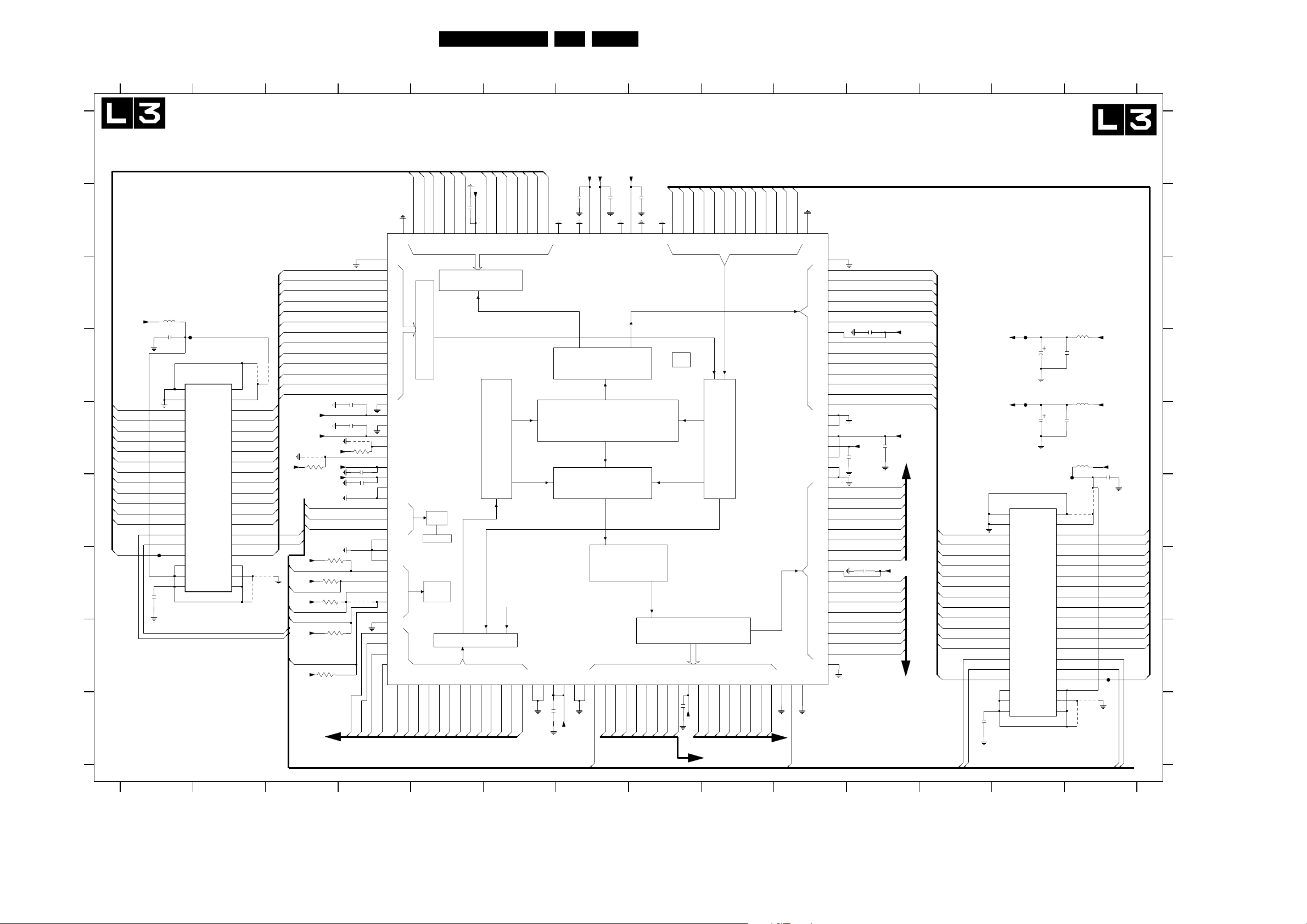
Feature Box 7 Panel: Falconic
1234
FALCONIC (FEATURE BOX 7)
A
B
C
+3.3VA
D
FB(11)
FB(10)
FB(09)
E
F
FB(08)
FB(07)
FB(06)
FB(05)
FB(04)
FB(03)
FB(02)
FB(01)
FB(00)
FB(12)
G
H
I
8204 000 64316
5716
2784
F224
100n
7717
MSM54V12222A
1
VSS1
VSS3
NC1
VCC3
DOUT11
DIN11
DOUT10
DIN10
2
DOUT9
DIN9
DOUT8
DIN8
DIN7
DOUT7
DOUT6
DIN6
DOUT5
DIN5
DOUT4
DIN4
DOUT3
DIN3
DOUT2
DIN2
DOUT1
DIN1
FIELD MEMORY
DIN0
DOUT0
SRCK
SWCK
RSTR
RSTW
WE
IE
VSS2
NC2
VCC121VCC2
RE
OE
F227
2782
2
3
4
5
6
7
8
9
10
11
12
13
14
15
16
17
18
19
20
100n
1234567891011121314
Circuit Diagrams and PWB Layouts
2785
100n
2786
100n
4716
3766 47K
2787
4720
MF(01)
1V5
1V5
1V5
1V5
1V5
1V5
1V5
1V5
100n2788
100n
MF(02)
YC0
YC1
YC2
YC3
YC4
YC5
YC6
YC7
UVC0
UVC1
UVC2
4713
4712
UVC0
UVC1
UVC2
UVC3
4714
YC0
YC1
YC2
YC3
YC4
YC5
YC6
YC7
REC
RSTR
CLK32
UVC3
REC
+3.3FA
CLK32
RSTR
+3.3FA
TRST
+3.3FA
TMS
+3.3FA
TD0
TDOA
+3.3FA
TCK
+3.3FA
+3.3FA
+2.5FB
4717
3767
47K
RSTR
SN-DA
SN-CL
+3.3FA
+3.3FA
+2.5FB
3782
47K
3773
47K
3781
47K
3783
47K
3774
47K
40
39
38
37
36
35
34
33
32
31
30
29
28
27
26
25
24
23
22
4715
L1
7718
SAA4992
MF(03)
1
2
3
4
5
6
7
8
9
10
11
12
13
14
15
16
17
18
19
20
21
22
23
24
25
26
27
28
29
30
31
32
33
34
35
36
37
38
39
40
MF(04)
VSS-C1
YC0
YC1
YC2
YC3
YC4
YC5
YC6
YC7
UVC0
UVC1
UVC2
UVC3
RE-C
VSS-C2
VSS-1
VDD-1
JUMP0
JUMP1
VDD-2
VSS-2
RAMTSTL
SN-RST
SN-DA
SN-CL
VSS-S
RAMTST2
TEST
TRST
TMS
TDI
TDO
TCK
VSS-AL
UVA0
UVA1
UVA2
UVA3
UVA4
41
MF(06)
FB(10)
FB(11)
159
158 157
160
YB0
YB1
VSS-B2
DECOMPRESS
SNERT
INTER
CONTROL
BST
UVA543UVA644UVA7
42
MF(09)
MF(08)
MF(07)
73F21RE AB 7.
5 6 7 8 9 1011121314
+3.3FA
+3.3FA
FB(06)
FB(07)
FB(08)
FB(09)
100n2803
156
155
154
153
YB2
YB3
YB4
YB5
VDD-B
COMPRESS
DNR
YA046YA147YA248YA349YA450YA551YA6
45
MF(14)
MF(13)
MF(12)
MF(11)
MF(10)
FB(01)
FB(02)
FB(03)
FB(04)
FB(05)
150
149
151
YB7
UVB0
UVB1
148
UVB2
152
YB6
LEFT MPRAM
VECTORS
YA7
RE-A
52
53
MF(18)
MF(17)
MF(16)
MF(15)
+2.5FB
FB(00)
147
UVB3
FB(12)
146
WE-B
145
VSS-B1
2802
100n
143
VSS-K
142
VDD-K
FALCONIC
DEINTERLACER
MOTION ESTIMATOR
UPCONVERSION
VDD-357VDD-4
56
100n
+2.5FB
VSS-FL
59
RE_F
RE-F
60
VSS-358VSS-4
VSS-A2
55
54
2789
+2.5FB
100n
2801
138
VDD-7
VECTORS
VECTORS
VERTICAL
PEAKING
YF(7)
YF(6)
YF(5)
100n
2800
136139140141144
135
137
VSS-7
VSS-E2
VERTICAL ZOOM
YF1
YF265YF364YF463YF562YF661YF7
6766
YF(4)
YF(3)
YF(2)
YF(1)
FE(12)
134
IE-E
PIXEL
PEAK
YF(0)
FE(00)
133
YF0
68
100n2790
UVE3
FE(01)
FE(02)
FE(03)
131
132
130
UVE1
UVE2
UVE0
RIGHT MPRAM
VDD-F
UVF5
UVF6
UVF7
69
72
71
70
UVF(7)
UVF(6)
UVF(5)
+3.3FA
L1
L2
FE(04)
129
YE7
UVF(4)
FE(05)
UVF4
73
128
YE6
UVF(3)
UVF3
74
FE(06)
127
YE5
UVF(2)
FE(07)
UVF2
75
126
YE4
UVF(1)
FE(08)
UVF1
76
125
YE3
FE(09)
124
YE2
UVF0
77
UVF(0)
L2
FE(10)
123
YE1
VSS-F2
78
CLK32
FE(11)
122
YE0
CLK32
79
121
VSS-E1
VSS-D2
VDD-D
UVD0
UVD1
UVD2
UVD3
WE-D
VSS-DI
VSS-6
VDD-6
VDD-5
VSS-5
VSS-G2
UVG0
UVG1
UVG2
UVG3
UVG4
UVG5
UVG6
UVG7
VDD-G
VSS-G1
VSS-CLK
80
YD0
YD1
YD2
YD3
YD4
YD5
YD6
YD7
YG0
YG1
YG2
YG3
YG4
YG5
YG6
YG7
120
119
118
117
116
115
114
113
112
111
110
109
108
107
106
105
104
103
102
101
100
99
98
97
96
95
94
93
92
91
90
89
88
87
86
85
84
83
82
81
100n
2797
2795
2798
+3.3FA
100n
100n
100n
UVG(0)
UVG(1)
UVG(2)
UVG(3)
UVG(4)
UVG(5)
UVG(6)
UVG(7)
YG(0)
YG(1)
YG(2)
YG(3)
YG(4)
YG(5)
YG(6)
YG(7)
2796
+3.3FA
+3.3FA
+2.5FB
L2
L2
YD0
YD1
YD2
YD3
YD4
YD5
YD6
YD7
UVD0
UVD1
UVD2
UVD3
WED
YD0
YD1
YD2
YD3
YD4
YD5
YD6
YD7
UVD0
UVD1
UVD2
UVD3
WED
CLK32
RSTR
2783
+3.3FA
+2.5FB
1
2
3
4
5
6
7
8
9
10
11
12
13
14
15
16
17
18
19
100n
F221
10u
F222
10u
7719
MSM54V12222A
VSS1
NC1
DOUT11
DIN11
DOUT10
DIN10
3
DOUT9
DIN9
DIN8
DOUT8
DOUT7
DIN7
DOUT6
DIN6
DIN5
DOUT5
DIN4
DOUT4
DIN3
DOUT3
DIN2
DOUT2
DOUT1
DIN1
FIELD MEMORY
DOUT0
DIN0
SWCK
RSTW
WE
IE
NC2
VCC120VCC2
VSS3
VCC3
SRCK
RSTR
VSS2
5719
+3.3VA
100n
2793
2794
5718
+2.5VB
2792
2791
100n
5717
+3.3VA
4722
4724
4723
4721
2799
100n
F226
RSTR
FE(11)
FE(10)
FE(09)
FE(08)
FE(07)
FE(06)
FE(05)
FE(04)
FE(03)
FE(02)
FE(01)
FE(00)
FE(12)
CLK32
F223
40
39
38
37
36
35
34
33
32
31
30
29
28
27
26
25
24
RE
23
OE
22
21
CL 36532021_012.eps
040403
2782 G1
2783 I12
2784 D1
2785 D4
2786 E4
2787 F4
2788 E4
2789 I6
2790 I8
2791 E14
2792 E13
A
2793 D14
2794 D13
2795 G11
2796 E11
2797 E11
2798 C11
2799 E14
2800 B8
2801 B7
2802 B7
2803 B5
3766 E4
B
3767 E3
3773 G3
3774 H3
3781 G3
3782 G3
3783 H3
4712 D3
4713 D2
4714 G2
4715 G2
4716 E4
4717 E3
C
4720 G4
4721 F14
4722 F14
4723 I14
4724 I14
5716 C1
5717 E14
5718 D14
5719 D14
7717 D1
7718 B4
D
7719 F13
F221 D13
F222 D13
F223 F14
F224 D1
F226 H14
F227 G1
E
F
G
H
I
Page 74
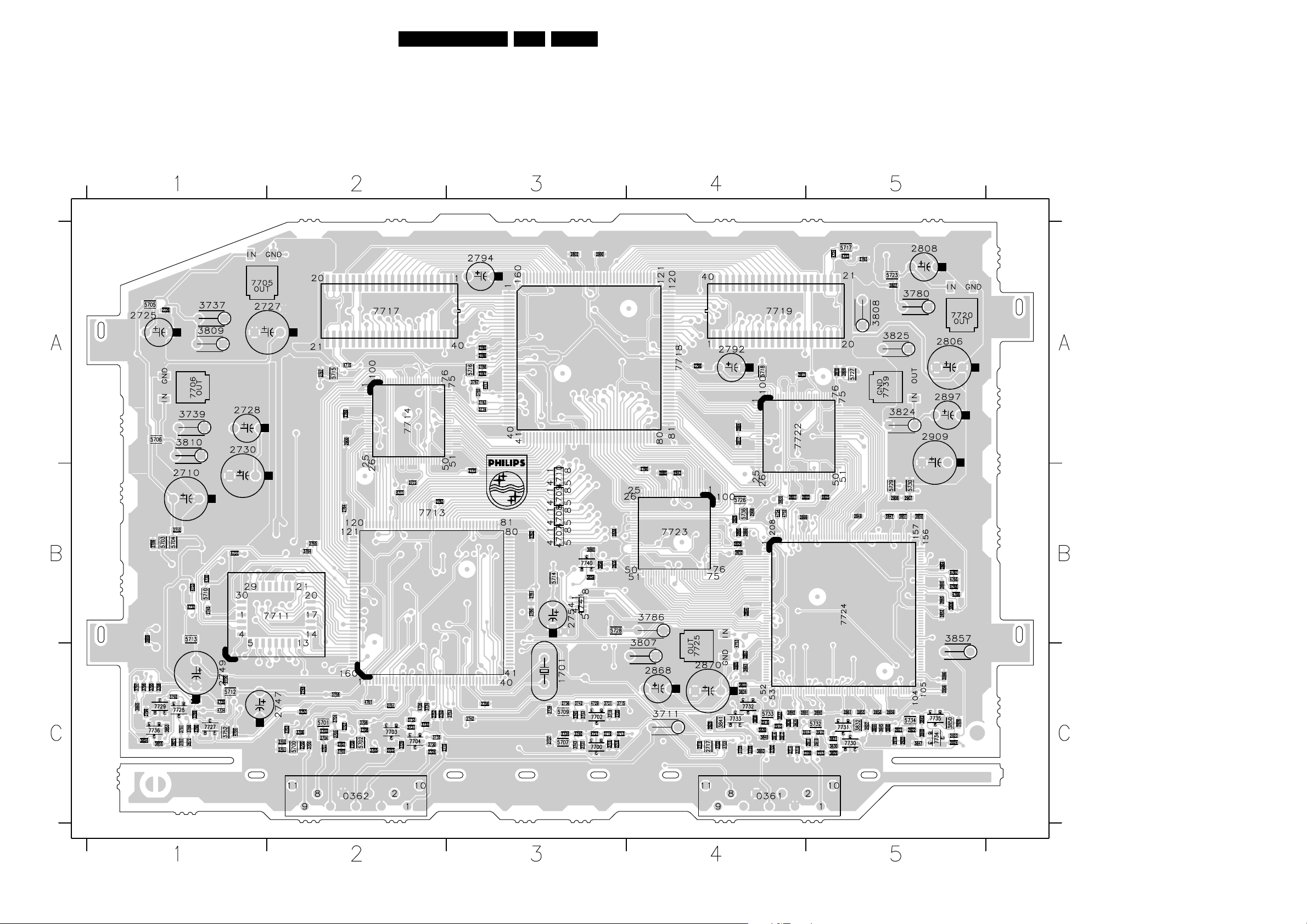
Circuit Diagrams and PWB Layouts
Layout Feature Box 7 Panel (Top View)
74F21RE AB 7.
0361 C4
0362 C2
1701 C3
2700 C2
2701 C2
2702 C2
2703 C2
2704 C2
2705 C2
2706 C2
2707 C2
2708 C2
2709 B1
2710 B1
2712 B1
2713 C5
2714 C4
2715 C2
2716 C4
2717 C4
2718 C3
2720 C3
2722 C4
2723 C2
2724 C2
2725 A1
2726 A1
2727 A2
2728 A1
2730 B1
2731 C3
2733 C3
2734 C3
2736 C3
2737 C3
2739 C3
2740 C2
2742 C3
2745 B1
2747 C2
2748 C2
2749 C1
2750 C1
2751 C2
2752 C2
2753 C3
2754 B3
2756 C3
2760 B3
2761 B3
2762 B3
2763 B2
2764 B2
2765 B2
2767 A2
2769 A2
2773 B2
2775 B3
2783 A5
2785 A3
2786 A3
2787 A3
2788 A3
2790 B4
2792 A4
2794 A3
2796 A4
2800 A3
2802 A3
2805 C4
2806 A5
2807 A5
2808 A5
2809 A5
2810 A5
2813 A4
2817 A4
2820 B4
2821 B4
2822 B4
2825 B5
2826 B4
2829 B4
2832 B4
2835 B3
2838 B3
2843 B4
2847 B5
2849 B5
2850 B5
2851 B5
2852 B5
2855 C5
2856 C5
2858 C5
2859 C5
2860 B5
2861 C5
2864 B5
2865 B5
2866 C5
2867 C4
2868 C4
2870 C4
2871 C1
2872 C1
2884 A4
2885 B4
2889 B4
2890 C5
2891 C4
2892 C4
2893 C4
2894 B4
2895 B4
2897 A5
2899 B4
2900 A2
2906 B5
2907 B5
2908 B4
2909 A5
2910 C5
2911 C5
2912 C5
2913 C5
2914 C4
2915 C4
2916 C4
2917 C4
2918 C5
2920 C5
2921 C5
2922 C5
2923 C5
2924 C5
2926 C5
2927 C5
2928 C4
3700 C2
3701 C2
3702 C2
3703 C2
3704 C2
3705 C2
3706 C2
3707 C2
3708 C2
3709 C5
3710 C4
3711 C4
3713 C3
3715 C3
3716 C3
3718 C3
3719 C3
3721 C3
3722 C4
3723 C4
3726 C4
CL 16532149_042.eps
061201
3728 C4
3729 C2
3730 C2
3731 C2
3732 C2
3733 C2
3734 C2
3735 C2
3737 A1
3739 A1
3740 C3
3742 C3
3743 C3
3745 C3
3752 C1
3753 C2
3758 C2
3764 B2
3767 A3
3774 A3
3780 A5
3782 A3
3783 A3
3786 B4
3787 C1
3788 C1
3789 C1
3790 C1
3791 C1
3792 C1
3793 C1
3794 C1
3795 C1
3796 C1
3797 C1
3798 C1
3806 B5
3807 B4
3808 A5
3809 A1
3810 A1
3824 A5
3825 A5
3829 C5
3830 C5
3831 C5
3832 C5
3833 C4
3834 C4
3835 C4
3836 C4
3837 C4
3838 C4
3839 C4
3840 C4
3841 C4
3844 C5
3845 C5
3846 C5
3847 C5
3848 C5
3849 C5
3850 C5
3853 C1
3854 C1
3855 C1
3857 B5
3858 B3
3859 B3
3860 B3
3863 C4
3865 C1
3999 B1
4700 C1
4701 C2
4707 B3
4708 B3
4709 B3
4710 B3
4711 B2
4715 A2
4717 A3
4723 A5
4724 A5
4726 C2
4727 C3
4729 C3
4730 B1
4731 B1
4732 B1
4733 B1
4734 C1
4735 C1
4741 B3
4752 B4
4753 C4
4754 B4
4765 B5
4766 B5
4767 B5
4768 B5
5700 C2
5701 C2
5702 C2
5703 B1
5704 B1
5705 A1
5706 A1
5707 C3
5709 C3
5710 B1
5712 C1
5713 B1
5714 B3
5715 A2
5716 A3
5717 A5
5718 A4
5723 A5
5726 B4
5727 A5
5728 B3
5729 B5
5730 B5
5732 C5
5733 C4
5734 C5
5736 B4
7700 C3
7702 C3
7703 C2
7704 C2
7705 A2
7706 A1
7711 B2
7713 B2
7714 A3
7717 A2
7718 A4
7719 A4
7720 A5
7722 A5
7723 B4
7724 B5
7725 C4
7727 C1
7728 C1
7729 C1
7730 C5
7731 C5
7732 C4
7733 C4
7734 C5
7735 C5
7736 C1
7739 A5
7740 B3
Page 75
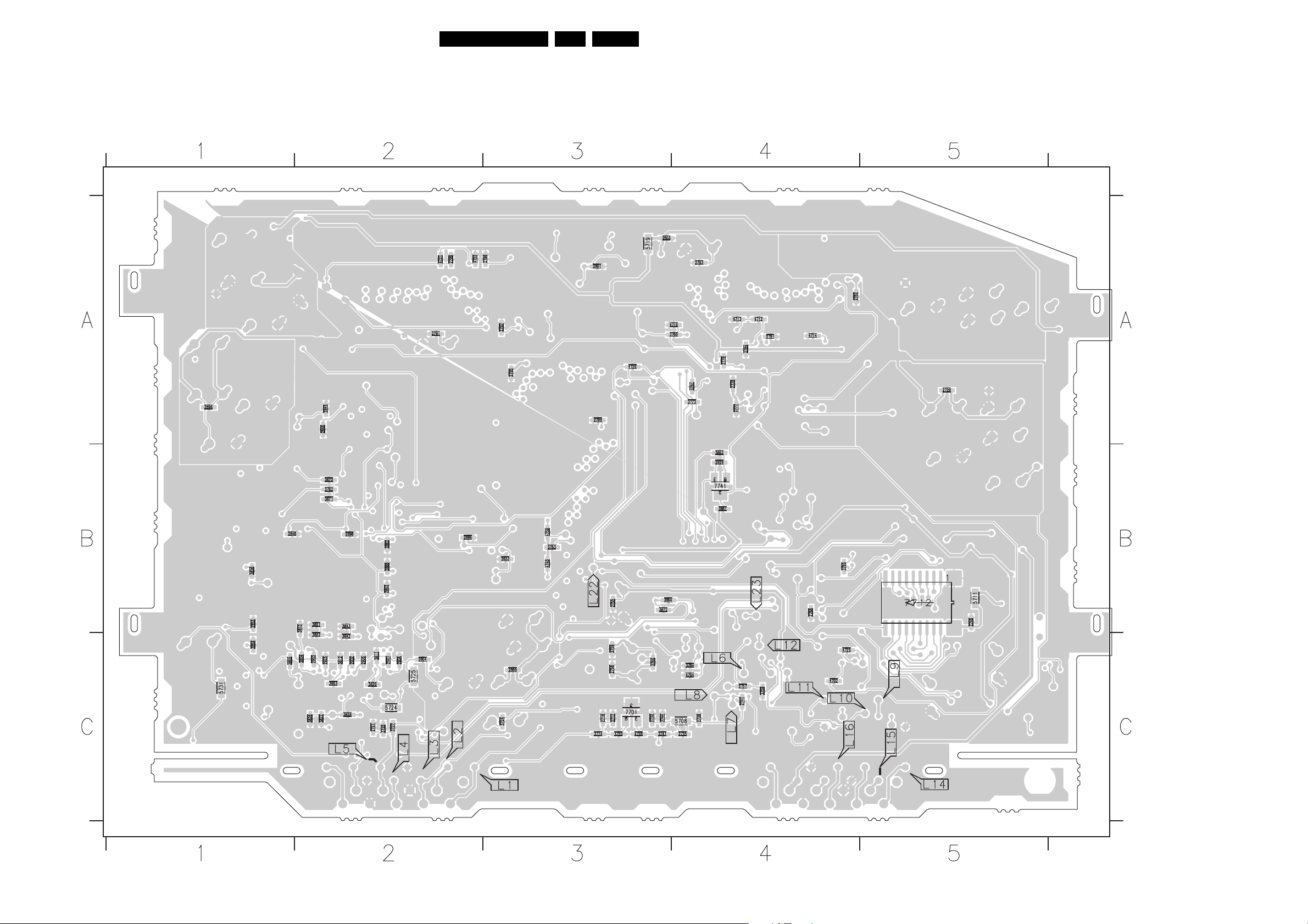
Circuit Diagrams and PWB Layouts
Layout Feature Box 7 Panel (Bottom View)
2719 C3
2721 C2
2729 A5
2732 C3
2735 C4
2738 C4
2741 C4
2746 B5
2755 B3
2757 C4
2758 C3
2759 C3
2766 B4
2777 A4
2778 A4
2779 A4
2781 A4
2782 A4
2784 A4
2789 A3
2791 A2
2793 A4
2795 A3
2797 A3
2798 A3
2799 A2
2801 A3
2803 A3
2804 C2
2833 B3
75F21RE AB 7.
2845 A2
2846 A2
2848 B1
2853 B1
2854 C1
2862 B2
2863 B2
2869 C3
2886 B2
2888 B2
2896 A1
2898 B2
2901 C2
2902 C2
2903 C2
2904 C2
2905 C2
2925 C2
2929 B4
3714 C3
3717 C3
3720 C3
3724 C3
3725 C2
3727 C2
3741 C3
3744 C3
3759 C4
3760 C3
3762 B2
3763 B3
3765 B4
3766 A4
3773 A4
3781 A4
3784 C4
3803 C2
3804 C2
3805 C1
3811 C2
3812 C2
3813 B2
3820 C2
3826 C2
3827 C2
3828 C2
3842 C2
3843 B2
3851 B2
3852 C2
3856 B1
3861 B4
3862 B4
3864 B3
3870 B2
3871 B2
3872 B3
4702 C4
4704 C4
4712 A4
4713 A4
4714 A4
4716 A4
4720 A3
4721 A2
4722 A2
4725 C4
4728 C3
4740 B3
4750 B3
5708 C4
5711 B5
5719 A3
5724 C2
5725 C2
5731 C1
7701 C3
7712 C5
7741 B4
CL 16532149_043.eps
191201
Page 76
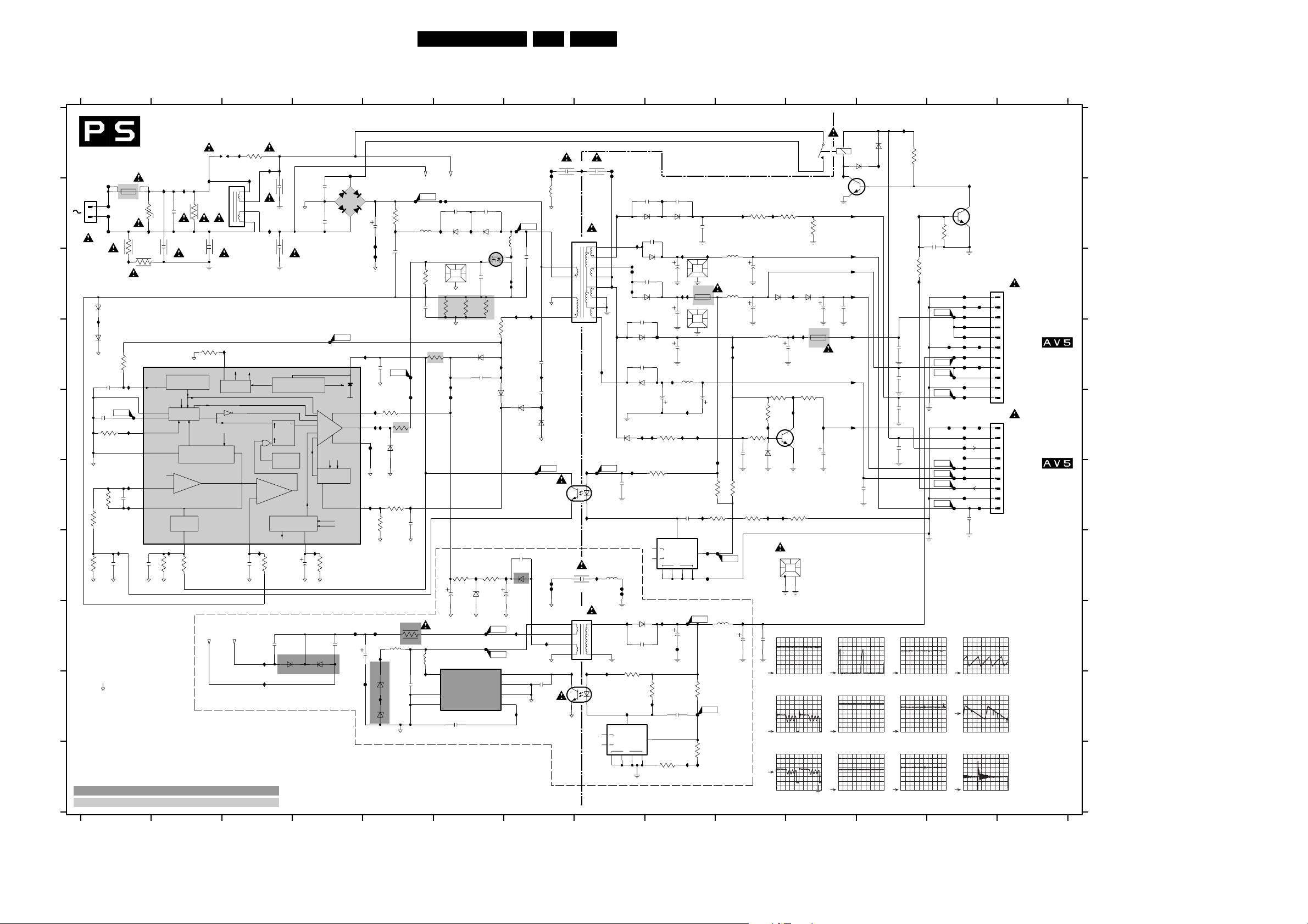
Power Supply
1
2
POWER SUPPLY
A
net_4mm
B
149V (0V)
0300
100-240 VAC
149V (0V)
F001
1
2
F004
1001
T 2,5 A E 250V
F002
F003
3001
I103
net_3.0mm
4M7
4M7
3000
3002
I102
net_1.6mm
I101
V
2002
2001
220p
I104
330n
net_1.6mm
RES
C
6005
1N4003
I124
0V (0V)
6006
GNDA
GNDA
3034
3035
GNDA
2014
2013
1n
3032
22K
15K
680R
1N4003
82p
2V6 (0V)
3033
2015
GNDA
3030
0V3
(0V)
I125
F071
2V5
(0V)
I127
2V5 (0V)
I128
15K
2049
I129
2V5 (0V)
I130
27n
82K
4n7
7001
MC44603A
8
9
10
15
12
14
13
GNDA
Vdem in
Sync
C
R standby
R standby
VOLTAGE
FEEDBACK
E/A OUT
2016
GNDA
DEMAGNETICATION
MANAGEMENT
Vdem out
Iref
OSCILLATOR
T
F
P
2.5V
ERROR
AMP
FOLDBACK
FOLDBACK INPUT
I131
15K
3036
100p
GNDA
(REDUCED FREQUENCY)
5
3037
D
E
F
G
H
( )
IN STANDBY
MEASURED
...
HOT GROUND
I
J
STANDBY SUPPLY REPAIR KIT: 3122 785 90390
MAIN SUPPLY REPAIR KIT: 3122 785 90400
1
23
1000
DSP
I106
net_1.6mm
5000
U-15D3
2M2
3003
RES
220p
2004
GROUNDING _STRIP
GNDB
GNDB
3031
I123
10K
2V5 (0V)
16
Rref
Vref
REFERENCE
BLOCK
Vosc prot
Vosc
Iref
STANDBY
CURRENT SENSE INPUT
0V9 (0V8)
180K
0V (0V)
GNDA
STB2 STB1
STANDBY_SUPPLY
Circuit Diagrams and PWB Layouts
456
net_1.6mm
net_1.6mm
GNDA
GNDA
Soft Start & Dmax
I133
11
2u2
2018
net_1.5mm
309V
(309V)
1N5062 (COL)
F005
net_1.6mm
2n2
2000
14
6000
2n2
2003
149V (0V)
F012
Vcc
UVLO1
OUTPUT
BUFFER
Vovp out
Vref
Vcc
OVERVOLTAGE
MANAGEMENT
OVERVOLTAGE
PROTECTION
UVLO1
Vref
22K
3039
GNDA
2201
6204
GBU4J
3
2
F006
F007
12V4 (12V)
I120
1
18V
12V (12V)
Vc
2
0V8 (0V)
3
GND
4
GNDA
1V6 (0V)
I134
6
F060
2202
F062
2005
GNDA
GNDA
I138
I136
F015
GNDA
F061
22u
I206
I137
6201
6202
309V (0V)
net_1.5mm
3010
220u
I111
2007
100n
2012
3043
150R
BAT254
GNDA
3041
1K8
3040
270R
5201
I179
net_2.1mm
308V
(313V)
BZT03-C
net_1.0mm
(200V)
BZT03-C
F013
F014
3042
33R
RES
249V
GNDA
456
I107
Iref
7
3
3005
100R
I105
2
1
3
4
Vref
enable
CURRENT
SENSE
I132
3038
2017
470p
149V (0V)
I201
I202
I108
220p
2053
GNDB
I109
220p
2054
GNDB
SUPPLY &
INITIALIZATION BLOCK
QSet
Latch
Reset
THERMAL
SHUTDOWN
Dmax & SOFT-START
CONTROL
Iref
2V1 (0V)
330R
GNDA
2200
6203
1N5062 (COL)
22K
net_2.1mm
1n5
6013
I135
2019
GNDA
3200
1R
2207
149V (0V)
STB2
F008
F009
5004
I176
377V (1V2)
10K
0001
3011
2050
100p
3016
22R
100n
308V (313V)
5202
I178
net_2.1mm
47p
STB1
F010
2006
net_2.1mm
470p
6002
I112
BYD33J
BYD33J
347V
(1V0)
STP6NC60
7000
0V8 (0V)
2020
GNDA
1R
1R
3012
3013
GNDA
6007
12V8 (12V)
BYD33D
2009
100p
I118
F070
12V2 (0V)
21V4
(17V5)
I121
3017
4K7
6008
220u
2011
RES
GNDA
GNDA
net_1.5mm
net_2.1mm
7200
TNY256
DRAIN4ENABLE
5
6
7
8
RES
SOURCE3
SOURCE4
SOURCE5
2204
100n
SOURCE2
SOURCE1
2052
470p
6014
G
2n2
0V (0V)
3014
3044
3K9
BZX79-C24
BYPASS
307V
(0V8)
1R
3015
6009
28V5
(22V0)
I122
2025
F072
F073
net_2.1mm
I113
D
S
I114
I180
I116
2R2
0V (0V)
I117
BYD33D
1N4148
BYD33J
47u
GNDA
I204
1V3 (1V2)
3
2
1
7
2030
F018
F017
220p
5005
GNDA
F011
5002
2008
6011
2206
100p
6010
GNDA
I207
5V9 (5V9)
5003
CT345D7
220p
I115
GNDA
12V4 (12V)
0V (0V)
GNDA
3
4
5
6
7
GNDA
89
2n2
2023
net_1.0mm
I139
2n2
2024
1V3 (0V)
F074
6012
1N4148
F016
7002
TCET1102
32
2V6 (0V) 7V5 (0V)
F064
F063
GNDA
1
2
I224
4
5
I208
2205
1n
32
GNDA
HOT COLD
7
I175
2203
220p
5200
CE165T
76F21RE AB 7.
8 9 10 11
2051
F019
F020
470p
I159
I169
14
I171
I177
14
16
15
14
13
12
I148
11
10
GNDB
I153
8V6 (0V5)
F024
5301
0V (0V)
7
6
I212I213
5V4 (5V4)
7203
TCET1102
4V4 (4V4)
5
NC
4
8
I141
2.5mm
GNDB
GNDB
0V
(0V)
net_1.2mm
F021
I149
0V
(0V)
4.0mm
0V
(0V)
0V
(0V)
GNDB
6108
1N4148
2116
F065
F066
I209
GNDB
I215
1
C
A
BYD33J
I145
RES
I225
STPS8H100
2111
6106
STPS745F
2128
100p
6107
BYD33J
I168
-12V1 (0V)
I170
100n
6310
SB340
2310
100p
3310
100R
REF
2367
GNDB
37V0 (0V2)
net_1.2mm
2127
2101
I142
100p
100p
6101
6110
BYD33J
2104
RES
I146
6102
BYD33J
2105
2107
RES
GNDB
6103
I167
3311
8
3109
100R
7011
TL431
5
4
I214
7202
TL431
1.2mm
9V0
(0V5)
F022
-9V1
(0V2)
I160
220u
3107
1K
NC
I210
F068
470R
2V5 (2V5)
3314
180R
2108
GNDB
2112
GNDB
2114
1
C
A
2311
GNDB
100n
2312
I151
I150
5V3 (0V)
3m3
5104
3u3
I158
I166
2118
100n
I217
COLD GROUND
9
62V2 (2V7)
2102
1m
GNDB
T4A
/250V
1101
0003
3m3
GNDB
47u
I165
I172
8
REF
F025
2367
F027
5V4 (5V4)
F067
1m
3312
3313
I216
470n
GNDB
I147
0002
2115
F023
3112
270R
2V5 (0V)
4K7
F069
3K9
I143 I144
5101
RES
22u
2106
RES
GNDB
5102
3u3
2109
GNDB
2.5mm
I154
I157
2117
100n
GNDB
68K
7K5
3111
3110
4K7
3113
F026
I211
5300
220u
2313
GNDB
10 11
3101
3K3
-0V7
(0V)
3108
3K9
GNDB
220u
1m
5103
3104
6109
GNDB
I173
2129
3102
3K3
1.2mm
8V3 (0V2)
I152
6104
BYD33J
I155
3u3
2113
GNDB
I162
4K7
3105
4K7
I164
1N4148
GNDB
I174
0005
12
GNDB
GNDB
F008
100n
50V / div DC
5µs / div
F011
100V / div DC
5µs / div
F012
20V / div DC
5µs / div
I156
1m
I163
4V9
(0V2)
7101
BC847B
3114
560R
HOT
G5PA
1400
RES
GNDB
6105
BYD33J
GNDB
3106
100R
2
3
3103
T4A
1102
I161
2119
GNDB
0V2 (5V4)
3K3
2110
/250V
COLD
1
4
6402
1N4148
I220
GNDB
+33V
+16V
+8V6
+7V7
2123
100n
47u
GNDB
+5V2
2.5mm
-7V7
POWER _VALID
4u7
F013
2V / div DC
5µs / div
F016
2V / div DC
5µs / div
F024
2V / div DC
10µs / div
2124
GNDB
0V3
(5V2)
7401
BC817
100n
1N4148
I219
12
I218
6401
0V15 (0V6)
I223
100n
2120
GNDB
2121
100n
GNDB
220n
2103
GNDB
100n
2126
GNDB
F026
500mV / div DC
10µs / div
F067
1V / div DC
10µs / div
F069
500mV / div DC
10µs / div
3401
22K
I222
3402
GNDB
GNDB
13 14
0V7 (0V)
10K
3403
100n
2401
22K
F028
F029
F032
F031
5V2 (0V)
F033
F034
F035
F036
F039
5V4 (5V4)
F038
F040
F042
8V8 (0V5)
F043
F044
F045
32V5 (2V6)
F047
F046
F049
5V3 (5V4)
F050
4V8 (0V2)
F051
F052
F053
F054
F055
0V5
F056
(3V3)
F057
F058
RES
GNDB
GNDB
F071
F072
F073
12 13 14
I221
7402
BC847B
PS 307
0307
1
F030
2
3
4
5
F037
6
7
F041
8
9
10
11
PS 306
0306
F048
1
2
3
4
7V6
5
(0V)
-9V2
6
(-0V4)
7
8
F059
9
2125
100n
1V / div DC
10µs / div
1V / div AC
2ms / div
100V / div DC
10µs / div
GND
GND
+5V2_FB
+5V2
+5V2
GND
+5VSTBY
+8V6
+8V6
GND
+33V
GND
POWER_ON
POWER_VALID
50HZ_60HZ
+7V7
-7V7
STANDBY
GND
+16V
CL16532023_037.eps
TO
0307
OUTPUT
SELECTION
+SUPPLY
TO
0306
OUTPUT
SELECTION
+SUPPLY
260901
3112 F10
3113 F10
3114 F11
3200 H5
3310 H8
3311 I9
3312 I9
3313 J9
3314 J9
3401 A12
3402 C12
3403 B13
3999 I11
5000 B2
5002 B7
5003 B7
5004 B5
5005 B7
5101 C10
5102 C10
5103 D10
5104 D9
5200 H7
5201 H5
5202 H5
5300 H10
5301 G8
6000 B4
6002 B6
6005 C1
6006 D1
6007 D6
6008 G6
6009 E6
6010 G7
6011 E7
6012 E7
6013 E5
6014 B6
6101 B9
6102 C9
6103 C9
6104 C10
6105 C11
6106 D8
6107 D8
6108 E8
6109 E10
6110 B9
6201 I5
6202 I5
6203 H3
6204 H4
6310 H8
6401 A12
6402 A12
7000 C6
7001 D1
7002 F7
7011 G9
7101 E11
7200 H6
7202 I9
7203 I8
7401 B12
7402 B13
F001 B1
F002 B1
F003 B1
F004 B1
F005 A4
F006 B5
F007 C5
F008 B5
F009 B6
F010 B6
F011 B7
F012 D4
F013 D5
F014 E5
F015 E5
F016 F7
F017 A7
F018 A7
F019 A8
F020 B8
F021 C8
F022 D9
F023 F9
F024 F8
F025 G9
F026 G10
F027 G9
F028 C13
F029 C13
F030 C13
F031 C13
F032 C13
F033 D13
F034 D13
F035 D13
F036 D13
F037 D13
F038 D13
F039 D13
F040 D13
F041 D13
F042 D13
F043 D13
F044 E13
F045 E13
F046 E13
F047 E13
F048 E13
F049 E13
F050 E13
F051 E13
F052 F13
F053 F13
F054 F13
F055 F13
F056 F13
F057 F13
F058 F13
F059 F13
F060 H4
F061 H5
F062 I4
F063 G7
F064 G7
F065 G8
F066 G8
F067 H9
F068 H9
F069 I9
F070 E6
F071 E1
F072 H6
F073 H6
F074 E7
F996 I11
F997 I11
F998 I11
F999 I11
I101 B2
I102 B1
I103 C1
I104 B2
I105 A3
I106 A2
I107 A3
I108 A3
I109 B3
I111 B5
I112 B6
I113 C7
I114 C7
I115 C7
I116 C7
I117 D7
I118 D6
I120 D5
I121 G6
I122 G7
I123 D3
I124 D1
I125 D1
I127 E1
I128 F1
I129 F1
I130 G1
I131 G2
I132 G3
I133 G4
I134 F5
I135 F5
I136 E5
I137 E5
I138 E5
I139 D7
I141 B8
I142 B9
I143 B10
I144 B10
I145 B8
I146 C9
I147 C9
I148 C8
I149 C8
I150 C9
I151 C9
I152 C11
I153 D8
I154 D10
I155 D11
I156 D11
I157 D10
I158 E9
I159 D8
I160 D9
I161 E11
I162 E11
I163 E11
I164 E10
I165 E9
I166 E9
I167 E9
I168 E8
I169 F8
I170 F8
I171 F8
I172 F9
I173 F10
I174 F10
I175 A8
I176 B6
I177 G8
I178 I5
I179 H5
I180 C7
I201 H3
I202 I3
I204 H7
I206 I5
I207 I7
I208 H7
I209 H8
I210 H9
I211 H10
I212 H8
I213 H8
I214 I9
I215 I8
I216 J9
I217 J9
I218 A12
I219 A12
I220 A11
I221 B13
I222 B12
I223 C12
I224 H7
I225 C8
0001 C6
0002 C9
0003 C9
0005 I12
0300 B1
0306 E13
0307 C13
1000 A3
A
1001 B1
1101 C9
1102 D11
1400 A11
2000 B4
2001 B2
2002 B2
2003 B4
2004 B2
2005 B5
2006 B6
2007 C5
B
2008 C7
2009 D6
2011 G6
2012 D5
2013 D1
2014 E1
2015 G1
2016 G1
2017 G3
2018 G4
2019 F5
2020 C6
C
2023 D7
2024 E7
2025 G6
2030 A7
2049 F1
2050 C5
2051 A8
2052 B6
2053 B3
2054 B3
2101 B9
2102 B9
D
2103 E12
2104 B9
2105 C9
2106 C10
2107 C9
2108 C9
2109 C10
2110 C11
2111 C8
2112 D9
2113 D10
2114 E9
E
2115 E9
2116 F8
2117 E10
2118 F9
2119 E11
2120 D12
2121 D12
2123 C11
2124 F12
2125 F13
2126 E12
2127 B9
F
2128 D8
2129 H10
2200 H3
2201 H4
2202 H4
2203 G8
2204 I6
2205 I7
2206 G7
2207 I5
2310 H8
2311 H9
G
2312 I9
2313 H10
2401 C13
3000 C1
3001 B1
3002 B1
3003 B2
3005 A3
3010 B5
3011 C5
3012 C6
3013 C6
H
3014 C6
3015 D6
3016 D6
3017 G6
3030 D1
3031 D2
3032 E1
3033 F1
3034 F1
3035 G1
3036 G2
3037 G2
I
3038 G3
3039 G4
3040 F5
3041 F5
3042 E5
3043 E5
3044 G6
3101 B10
3102 B11
3103 B11
3104 E10
3105 E10
J
3106 E11
3107 E9
3108 E10
3109 F9
3110 F10
3111 F9
Page 77
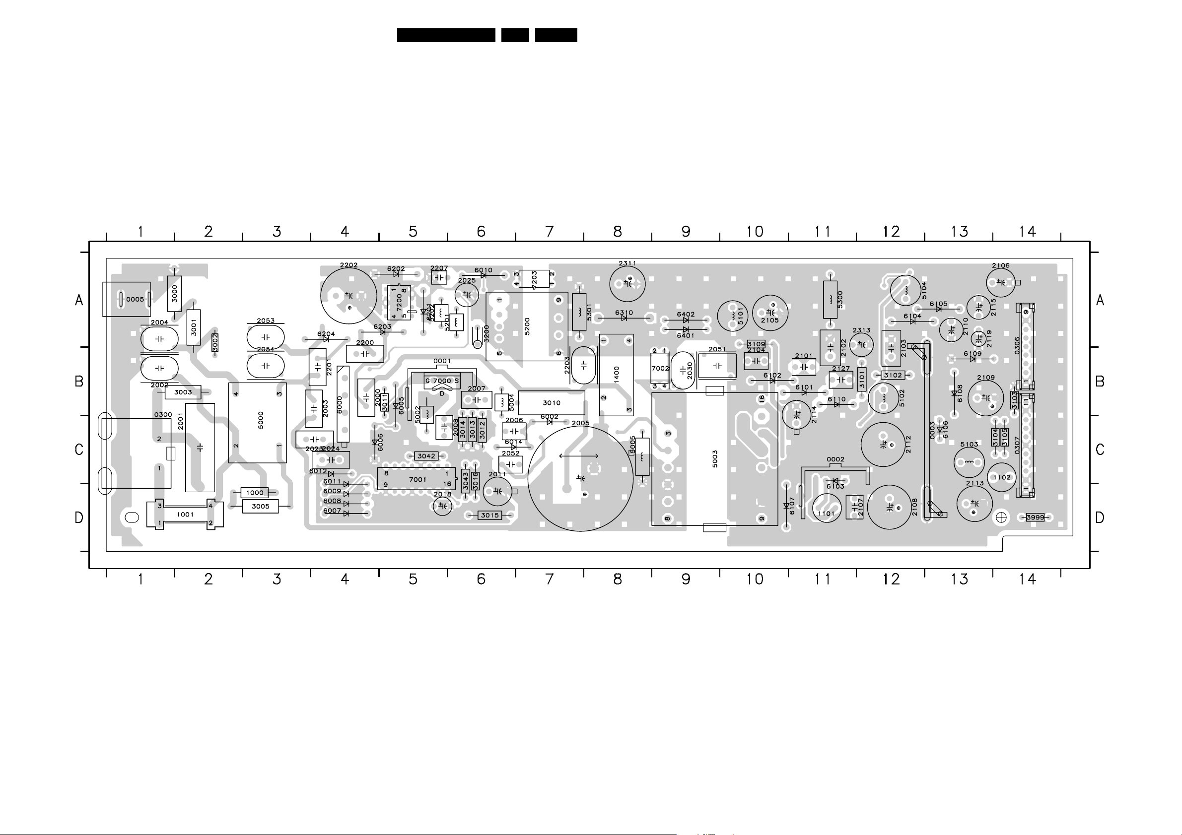
Circuit Diagrams and PWB Layouts
Layout Power Supply (Top Side)
77F21RE AB 7.
0001 B5
0002 C11
0005 C13
0005 A1
0300 B1
0306 A14
0307 C14
2105 A10
2106 A14
2107 D12
2108 D12
2109 B13
2110 A13
2112 C12
3103 B14
3104 C14
3105 C14
3109 A10
3200 A6
3999 D14
5000 C3
6105 A13
6106 C13
6107 D11
6108 B13
6109 B13
6110 B11
6201 A5
1000 D3
1001 D2
1101 D11
1102 C14
1400 B8
2000 B4
2001 C2
2113 C13
2114 B11
2115 A14
2119 A13
2127 B11
2200 A4
2201 B4
5002 B5
5003 C9
5004 B6
5005 C8
5101 A10
5102 B12
5103 C13
6202 A5
6203 A5
6204 A4
6310 A8
6401 A9
6402 A9
7000 B5
2002 B1
2003 B4
2004 A1
2005 C7
2006 C6
2007 B6
2008 C6
2202 A4
2203 B7
2207 A5
2311 A8
2313 A12
3000 A1
3001 A2
5104 A12
5200 A7
5201 A5
5202 A5
5300 All
5301 A8
6000 B4
7001 C5
7002 B9
7200 A5
7203 A7
2011 C6
2018 D5
2023 C4
2024 C4
2025 A6
2030 B9
2051 B9
3002 A2
3003 B2
3005 D3
3010 B7
3011 B5
3012 C6
3013 C6
6002 C7
6005 B5
6006 C5
6007 D4
6008 D4
6009 D4
6010 A6
2052 C6
2053 A3
2054 B3
2101 B11
2102 B11
2103 B12
2104 B10
3014 C6
3015 D6
3016 C6
3042 C5
3043 C6
3101 B12
3102 B12
6011 C4
6012 C4
6014 C6
6101 B11
6102 B10
6103 D11
6104 A12
CL 16532023_038.eps
210901
Page 78
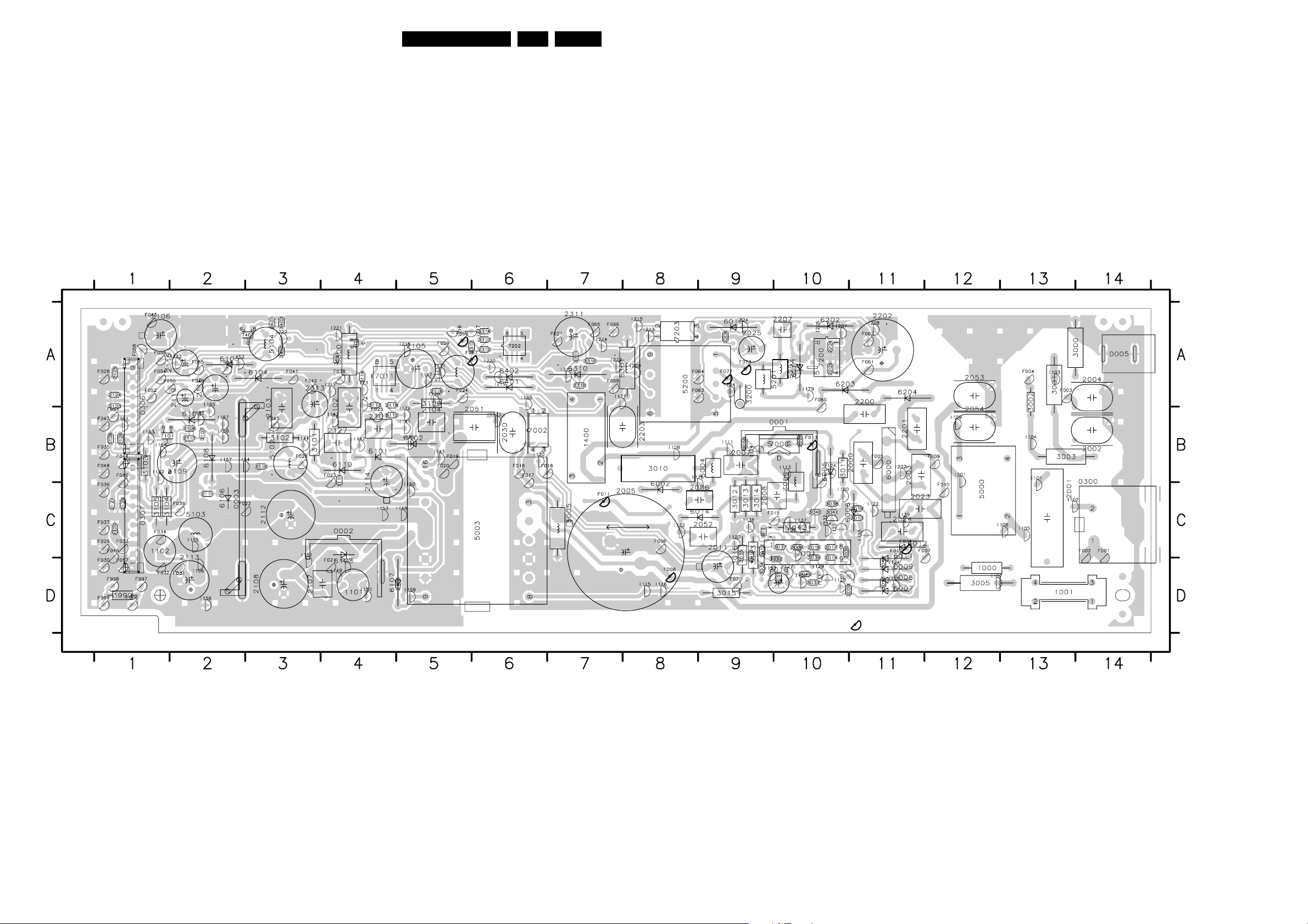
Circuit Diagrams and PWB Layouts
Layout Power Supply (Bottom Side)
78F21RE AB 7.
0001 B10
0002 C4
0003 C2
0005 A14
0300 B14
0306 A1
0307 C1
1000 D12
1001 D13
1101 D4
1102 C1
1400 B7
2000 B11
2001 C13
2002 B14
2003 B11
2004 A14
2005 C8
2006 C9
2007 B9
2008 C9
2009 D10
2011 C9
2012 C9
2013 C11
2014 C10
2015 C9
2016 C10
2017 C10
2018 D10
2019 C11
2020 B10
2023 C11
2024 C11
2025 A9
2030 B6
2049 D10
2050 B9
2051 B6
2052 C9
2053 A12
2054 B12
2101 B4
2102 B4
2103 B3
2104 B5
2105 A5
2106 A1
2107 D3
2108 D3
2109 B2
2110 A2
2111 C2
2112 C3
2113 C2
2114 B4
2115 A1
2116 A5
2117 B2
2118 A4
2119 A2
2120 C1
2121 C1
2123 A1
2124 A1
2125 A1
2126 B1
2127 B4
2128 D5
2129 C1
2200 A11
2201 B11
2202 A11
2203 B8
2204 A10
2205 A10
2206 A9
2207 A10
2310 A7
2311 A7
2312 A6
2313 A3
2401 A3
3000 A13
3001 A13
3002 A13
3003 B13
3005 D12
3010 B8
3011 B10
3012 C9
3013 C9
3014 C9
3015 D9
3016 C9
3017 D11
3030 C10
3031 D10
3032 D10
3033 D10
3034 D9
3035 C9
3036 C10
3037 C10
3038 C10
3039 C10
3040 C10
3041 C10
3042 C10
3043 C9
3044 D11
3101 B3
3102 B3
3103 B1
3104 C1
3105 C1
3106 B1
3107 B2
3108 B2
3109 A5
3110 B3
3111 B4
3112 B4
3113 A4
3114 A4
3200 A9
3310 A7
3311 A7
3312 A6
3313 A6
3314 A6
3401 A4
3402 A3
3403 A3
3999 D1
5000 C12
5002 B10
5003 C6
5004 B9
5005 C7
5101 A5
5102 B3
5103 C2
5104 A3
5200 A8
5201 A10
5202 A10
5300 A4
5301 A7
6000 B11
6002 C8
6005 B10
6006 C10
6007 D11
6008 D11
6009 D11
6010 A9
6011 C11
6012 C11
6013 C9
6014 C9
6101 B4
6102 B5
6103 D4
6104 A3
6105 A2
6106 C2
6107 D4
6108 B2
6109 B2
6110 B4
6201 A10
6202 A10
6203 A10
6204 All
6310 A7
6401 A6
6402 A6
7000 B10
7001 C10
7002 B6
7011 A4
7101 B1
7200 A10
7202 A6
7203 A8
7401 A4
7402 A3
F001 C14
F002 C14
F003 A13
F004 A13
F005 B11
F006 C8
F007 C11
F008 D8
F009 B12
F010 C12
F011 C7
F012 C11
F013 B10
F014 B10
F015 C9
F016 B6
F017 B6
F018 B6
F019 B5
F020 B5
F021 D4
F022 C2
F023 B4
F024 A5
F025 B4
F026 B3
F027 A7
F028 A1
F029 C1
F030 D1
F031 D2
F032 D1
F033 C1
F034 C1
F035 B1
F036 C1
F037 C1
F038 A4
F039 C2
F040 B1
F041 A3
F042 A3
F043 A1
F044 B1
F045 B3
F046 C1
F047 B1
F048 B1
F049 A2
F050 A1
F051 B1
F052 A1
F053 A2
F054 A1
F055 A2
F056 A1
F057 D1
F058 A1
F059 A5
F060 A10
F061 All
F062 A11
F063 A8
F064 A8
F065 A7
F066 A7
F067 A5
F068 A7
F069 A5
F070 D9
F071 D10
F072 A9
F073 A9
F074 C11
F996 D1
F997 D1
F998 D1
F999 D1
I101 B13
I102 C13
I103 A13
I104 B13
I105 C13
I106 C13
I107 D12
I108 B8
I109 B12
I111 B9
I112 C8
I113 B10
I114 B9
I115 D8
I116 D8
I117 D11
I118 D10
I120 C9
I121 D11
I122 C11
I1221 A4
I1222 A3
I1223 A2
I1224 A9
I1225 D4
I123 D9
I124 B10
I125 C10
I127 D10
I128 D10
I129 D10
I130 B6
I131 C10
I132 C10
I133 D10
I134 C10
I135 C11
I136 C10
I137 C10
I138 C9
I139 C11
I141 B5
I142 B4
I143 B4
I144 B3
I145 B5
I146 B5
I147 A5
I148 C5
I149 D4
I150 D4
I151 C3
I152 A2
I153 C4
I154 B2
I155 C2
I156 D2
I157 B2
I158 D2
I159 D5
I160 C5
I161 B1
I162 B1
I163 B1
I164 B1
I165 A2
I166 B2
I167 B2
I168 B2
I169 A6
I170 A5
I171 A5
I172 B5
I173 A4
I174 A4
I175 B6
I176 B8
I177 A7
I178 A10
I179 A10
I180 C10
I201 B12
I202 B11
I204 A9
I206 A10
I207 A10
I208 A11
I209 A8
I210 A7
I211 A4
I212 A7
I213 A8
I214 A7
I215 A8
I216 A5
I217 A6
I218 A5
I219 A6
I220 A6
I221 A4
I222 A3
I223 A2
I224 A9
I225 D4
NOTE: SERVICE TESTPOINTS ARE ACCENTUATED BY SYMBOL AND BOLD IN MAPPING
CL 16532023_039.eps
250901
Page 79
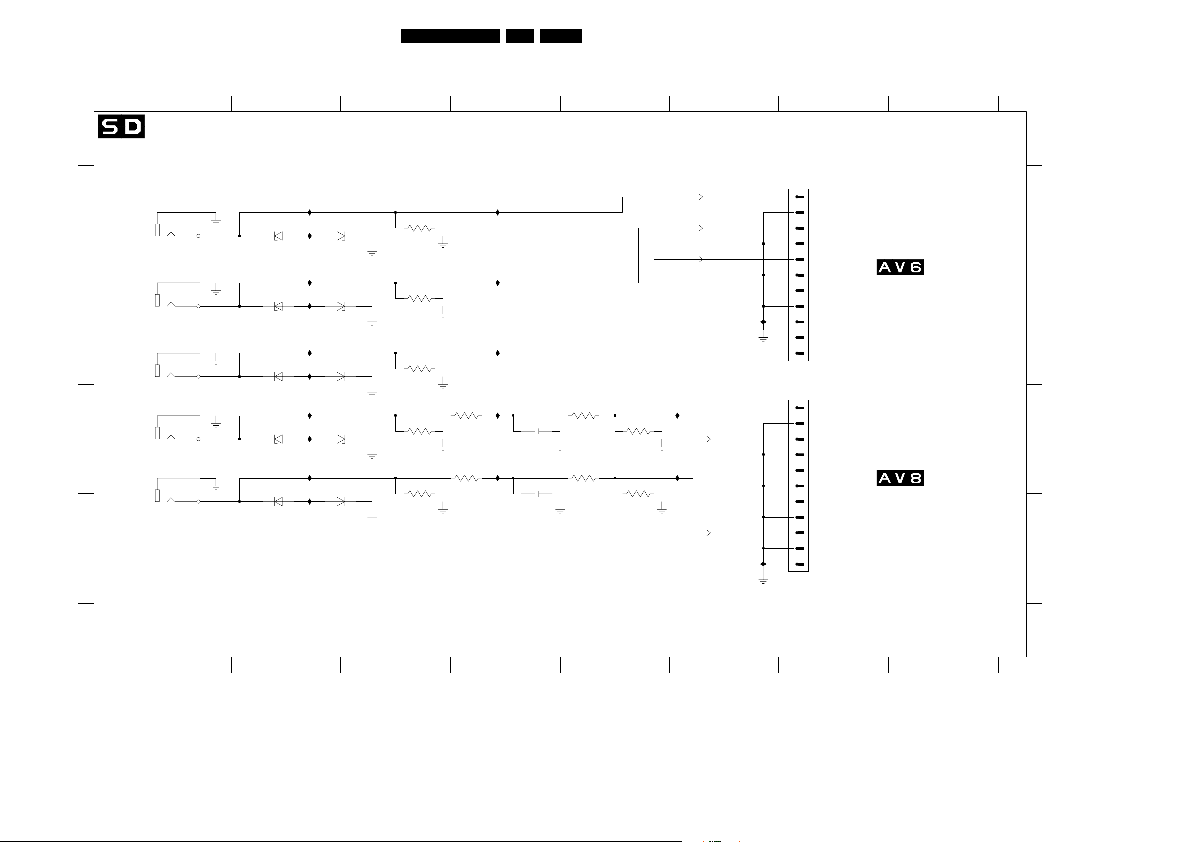
SD-Connector
Circuit Diagrams and PWB Layouts
79F21RE AB 7.
A
B
C
D
1
SD-CONNECTOR
(Europe only)
DVD
CINCH
INPUTS
Y
PB
PR
L
R
0360-C
YKC21-5637
0360-B
YKC21-5637
0360-A
YKC21-5637
0361-A
YKC21-5620
0361-B
YKC21-5620
5
6
0V0
3
4
0V0
1
2
0V0
1
2
0V0
3
4
0V0
2
6001
BZM55-C33
6003
BZM55-C33
6005
BZM55-C33
6007
BZM55-C33
6010
BZM55-C33
1001
1002
1003
1004
1005
1006
1007
1008
1009
1010
6002
BZM55-C33
6004
BZM55-C33
6006
BZM55-C33
6008
BZM55-C33
6009
BZM55-C33
345678
0304
0305
EH-S
0V0
0V0
0V0
0V0
0V0
8V8
0V0
EH-S
3V6
0V0
0V0
0V0
0V0
3V1
TO
AV304
YPBPR-YUV-MATRIX
TO
AV305
AUDIO+CONTROL
A
B
C
D
3002
75R
3003
75R
3004
75R
3007
33K
3011
33K
3005
1K
3009
1K
1011
1012
1013
1014
1015
2006
100p
2010
100p
3006
3K3
3010
3K3
3008
10K
3012
10K
1016
1017
Y_SD
PB_SD
PR_SD
SNDL_SD
SNDR_SD
1018
1019
1
2
3
4
5
6
7
8
9
10
11
1
2
3
4
5
6
7
8
9
10
11
0304 A7
0305 C7
0360-A B1
0360-B B1
0360-C A1
0361-A C1
0361-B C1
1001 A2
1002 A2
1003 A2
1004 B2
1005 B2
1006 B2
1007 C2
1008 C2
1009 C2
1010 C2
1011 A4
1012 A4
1013 B4
1014 C4
1015 C4
1016 C6
1017 C6
1018 B6
1019 D6
2006 C4
2010 C4
3002 A3
3003 B3
3004 B3
3005 C4
3006 C5
3007 C3
3008 C5
3009 C4
3010 C5
3011 C3
3012 C5
3999 D1
6001 A2
6002 A3
6003 B2
6004 B2
6005 B2
6006 B2
6007 C2
6008 C2
6009 C2
6010 C2
F998 D1
F999 D1
1
CL 16532023_040.eps
250901
2345678
Page 80
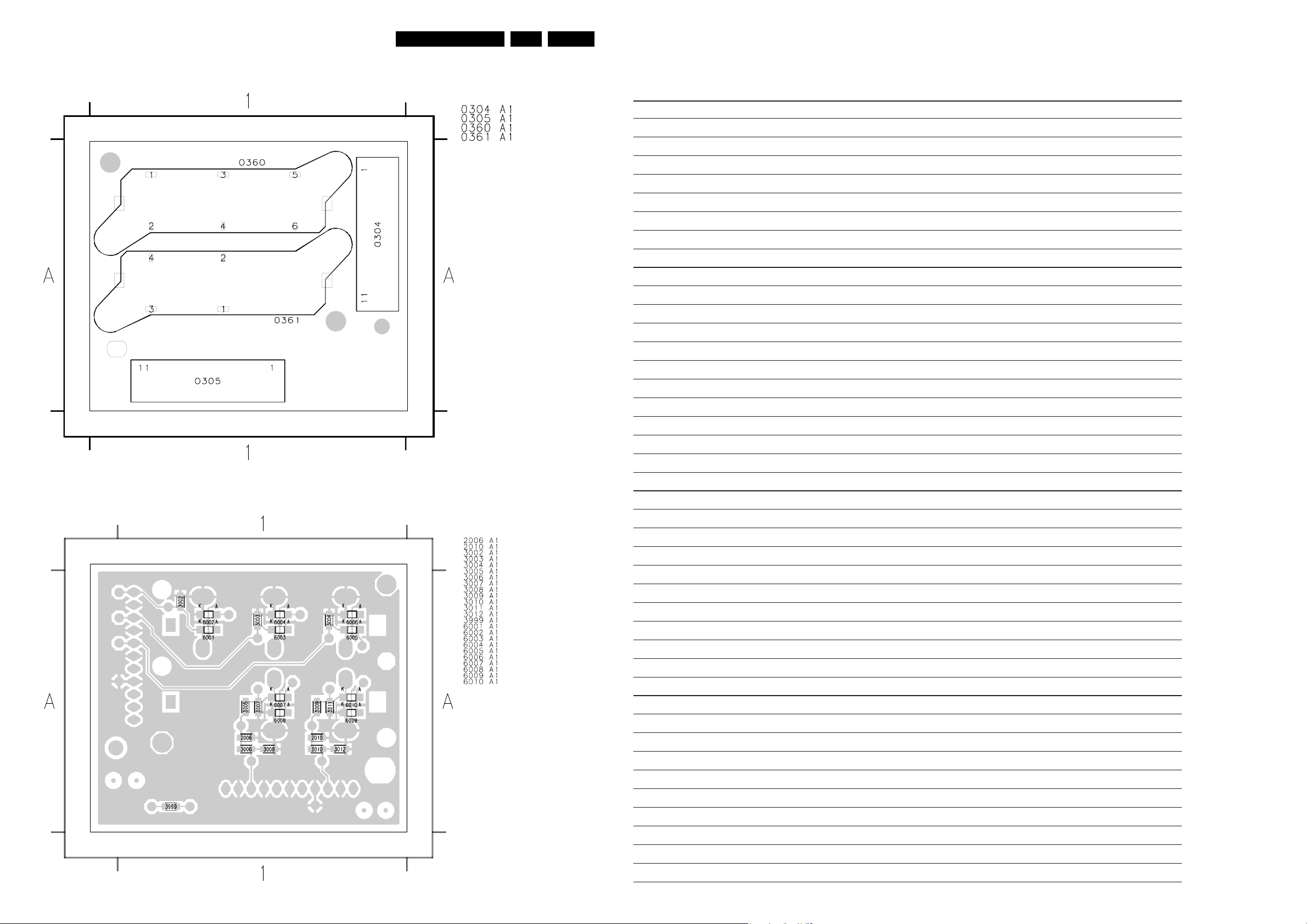
Circuit Diagrams and PWB Layouts
Layout SD-Connector (Top Side)
80F21RE AB 7.
Personal Notes:
Layout SD-Connector (Bottom Side)
CL 16532023_041.eps
200901
CL 16532023_042.eps
200901
Page 81
8. Electrical Alignments
Index of this chapter:
1. General Alignment Conditions
2. Hardware Alignments
3. Software Alignments
4. Option Settings
Notes:
• The Service Default Mode (SDM) and Service Alignment
Mode (SAM) are described in chapter 5. Menu navigation
is done with the CURSOR UP, DOWN, LEFT AND RIGHT
keys of the remote control transmitter.
• Figures below can deviate slightly from the actual product,
due to different set designs.
8.1 General Alignment Conditions
Perform all electrical alignments under the following conditions:
• Power supply voltage: 230 V_ac ± 10%, 50 Hz ± 5%.
• Allow the set to warm up for approximately 20 minutes.
• Voltages and waveforms are measured in relation to tuner
earth (with exception to the voltages on the primary side of
the power supply).
Caution: never use heatsinks as ground.
• Test probe: Ri > 10 MOhm, Ci < 20 pF.
Before performing any alignments, set the receiver box to the
following settings:
• Dynamic contrast: OFF (via the PICTURE menu).
• Active control: OFF (via the remote control. The ACTIVE
CONTROL key is the key between the smart keys, and
toggles Active Control ON and OFF).
• Smart Picture mode: ECO.
8.2 Hardware Alignments
8.2.1 40.4 MHz Neighbour-channel Sound Trap Alignment
1. Tune to a checker board test pattern (system PAL B/G with
a carrier frequency of 475.25 MHz).
2. Connect an oscilloscope to pin 19 (CVBS out) of the
SCART1 connection and trigger line frequent.
3. Align the coil L5103 (diagram K1) completely downwards
(see figure "SSP topview").
4. Align the coil upwards untill under- and overshoot arise at
the black/white and white/black transitions in the video
signal (see figure "Waveform sound trap alignment").
5. Align the coil downwards again, untill above mentioned
under- and overshoot just disappears.
SSP
0356
SAM
SDM
1
2
3
Electrical Alignments
Figure 8-2 Waveform sound trap alignment
8.3 Software Alignments
Notes:
• Alignments are stored automatically
• Dealer option settings are stored automatically
• Service option settings must be stored with the STORE
OPTIONS item in the top level SAM menu. It is not
necessary to turn the receiver box OFF and back ON in
order to store the values in NVM.
Put the set in SAM mode (see chapter 5). Now you can select
the following alignments:
1. GENERAL:
–LUMA GAIN
–IF AFC
–IF LPRIME AFC
– TUNER AGC
– BLEND INTENSITY
– FBX TEST PATTERN
2. DRIVE:
– TEST PATTERN
–RED
– GREEN
–BLUE
– RED BL OFFSET
– GREEN BL OFFSET
3. LUM. DEL:
– LUM. DELAY PAL BG
– LUM. DELAY PAL I
– LUM. DELAY SECAM
– LUM. DELAY BYPASS
8.3.1 GENERAL Alignments
LUMA GAIN
This item has a fixed value of "3" (for EU/AP).
CL 86532057_006.AI
170798
EN 81F21RE AB 8.
L5103
40.4 MHz
ALIGNMENT
Tuner
Figure 8-1 SSP top view
CL 86532057_004a.AI
240798
IF AFC
Connect the RF output of a video pattern generator to the
antenna input.
From the generator, supply a PAL B/G TV signal with a signal
strength of at least 1 mV and a frequency of 475.25 MHz.
Alignment procedure:
1. Go to the INSTALL menu.
2. Select MANUAL INSTALLATION.
3. Tune the TV-set to the system and frequency described
above via SEARCH - 475.00 - OK.
4. If the frequency shown in the FINE TUNE line (after the
SEARCH is completed) is between 475.18 MHz and
475.31 MHz, you do not need to realign the IF AFC.
Page 82
EN 82 F21RE AB8.
Electrical Alignments
5. If the frequency lies outside this range, adjust the
frequency in the FINE TUNE line to 475.25 MHz and
STORE the program (this is very important because this
will disable the AFC algorithm).
6. Navigate to the SAM main menu and select ALIGNMENTS
- GENERAL - IF AFC.
7. During the IF AFC parameter adjustment, there is OSD
feedback at the top of the screen.
8. This OSD feedback will contain one of four messages:
Table 8-1 AFC Alignment feedback
AFC-window AFC-frequency versus reference
Out High
In High
*In* *Low*
Out Low
The first item (IN or OUT) informs you whether you are in or out
of the AFC window. The second item (HIGH or LOW) informs
you whether the AFC frequency is too high or too low.
1. Adjust the IF AFC parameter until the first value is within
the AFC window (= IN).
2. Next, adjust the IF AFC parameter until the second value is
LOW.
3. After adjustment, STORE the value.
4. Return to the INSTALL menu.
5. Select MANUAL INSTALLATION - SEARCH - 475.00 - OK
and STORE. This will turn the AFC algorithm ON again.
Service tip: If you do not trust the frequency accuracy of your
service generator, connect it to a "good" TV set and check it
with the FINE TUNE line.
You can also use this pattern as a picture generator for the Flat
TV plasma monitor (for example, for checking cell defects,
interpretation of the ADC/DAC converters, etc).
Important: Be sure to set this pattern to OFF again when it is
no longer needed, since it will not be automatically disabled
when SAM is exited.
8.3.2 DRIVE Alignments
TEST PATTERN
The TEST PATTERN is not really needed for the alignment of
the Receiver box. It can be used in the TV configuration as a
test pattern to align the white colour temperatures of the
monitor. However, the monitor itself (as a stand alone unit) can
also be aligned in other ways (described in the Service Manual
of the TV monitor).
RGB Output Amplitude Adjustment
1. Load the RGB output (sub-D connector AV303) of the
Receiver box with a TV monitor (or match RGB output lines
with 75 ohm resistors, if no monitor is available), and
measure the outputs with an oscilloscope.
2. Apply an artificial white CVBS signal (1 V_pp white-to-topsync, with a 0.3 V sync amplitude) to the external 2 input.
3. Set LUMA GAIN to a value of "3" (via the SAM menu
ALIGNMENTS - GENERAL).
4. Set RED, GREEN, and BLUE to "24" (via the SAM menu
ALIGNMENTS - DRIVE).
5. Set RED BL OFFSET and GREEN BL OFFSET to "7".
6. Adjust the gain (with the RED, GREEN, and BLUE slider
bars) until the oscilloscope-measured values for R, G, and
B are 700 mV ± 10 mV with respect to the front porch of the
signal.
IF LPRIMEAFC
Same procedure as described above but with other signal
source (SECAM L').
TUNER AGC
Connect the RF output of a video pattern generator to the
antenna input.
From the generator, supply an PAL B/G TV signal with a signal
strength of approximately 2 mV and a frequency of 475.25
MHz.
Measure the DC voltage on pin 1 of the Tuner (item 1102). You
can adjust this voltage by adjusting the TUNER AGC item in the
SAM menu. Alignment is correct when the DC voltage is just
below 3.8 V.
BLEND INTENSITY
This adjustment aligns the level of transparency of the menu
display that is blended into the main display. Use this alignment
when the main microprocessor or the HOP IC is replaced.
1. Set the BRIGHTNESS, CONTRAST, and COLOR values
(in the PICTURE menu) at the midpoint.
2. Using a video pattern generator, apply a signal with a
100% white video pattern to the set.
3. Connect an oscilloscope to the “Red” output of the
Receiver box (pin 1 of the MONITOR OUT sub-D
connector) and measure the Red output level.
4. Align the BLEND INTENSITY parameter so that the
blended signal is 65 % of the black/white amplitude. This
ratio will be about 0.45 V (blended signal) to 0.7 V (full
white signal).
8.3.3 LUM. DELAY Alignments
With this alignment, you place the luminance information
directly on the chrominance information (brightness is pushed
onto the colour). Input a colour bar or grey scale pattern as a
test signal.
LUM. DELAY PAL BG
Set value to "12". If the luminance signal referred to the
chrominance signal still has a time delay, adjust the value to
solve this.
LUM. DELAY PAL I
Set value to "12". If the luminance signal referred to the
chrominance signal still has a time delay, adjust the value to
solve this.
LUM. DELAY SECAM
Set value to "11". If the luminance signal referred to the
chrominance signal still has a time delay, adjust the value to
solve this.
LUM. DELAY BYPASS
Set value to "10". If the luminance signal referred to the
chrominance signal still has a time delay, adjust the value to
solve this.
FBX TEST PATTERN
When this pattern is switched on, the set will display a picture
that slowly changes from black to white, and vice versa. Use
this pattern to check the functionality of the circuitry behind the
FBX and the FBX function itself.
Page 83
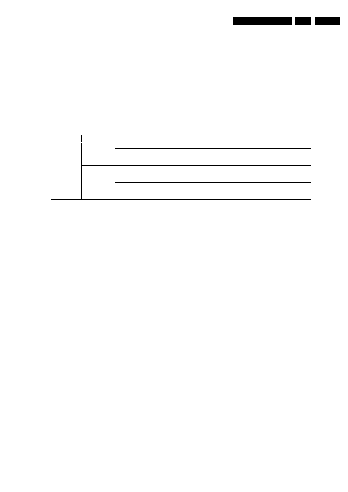
Electrical Alignments
EN 83F21RE AB 8.
8.4 Option settings
8.4.1 Introduction
The microprocessor communicates with a large number of
(I2C) ICs in the set. To ensure good communication and make
digital diagnosis possible, the microprocessor has to know
which ICs to address. The presence or absence of specific ICs
or functions is made known by means of the option codes.
8.4.2 Dealer Options
Select this sub-menu to set the initialisation codes (= options)
of the set via text menu's.
Menu name Subjects Options Physically in set
Personal
Options
Auto Store
Mode (for EU)
Txt Preference
(for EU)
Note:
Above overview gives the menu items for all regions (EU/AP/US). The correct settings differs per region (see Option Numbers).
Yes Video mute active when there is no signal detected Picture Mute
No Noise when there is no signal detected
Yes TV starts up with language selection menu Virgin Mode
No TV does not start up with language selection menu
None Auto Store mode disabled (not in installation menu)
PDC-VPS Auto Store mode via ATS (Automatic Tuning System) enabled
TXT page Auto Store mode via ACI (Automatic Channel Installation) enabled
PDC-VPS-TXT Auto Store mode via ATS or ACI enabled
FLOF Preference to FLOF (Full Level One Features) teletext
TOP Preference to TOP (Table Of Pages) teletext
All options codes can be manipulated using both the Option
Numbers and/or the Option menu.
All hardware related options are incorporated under the
heading SERVICE OPTIONS in the SAM main menu.
All software related options are incorporated under the heading
DEALER OPTIONS in the SAM main menu.
After you have changed the option(s), save them via the
STORE OPTIONS command. The new option setting is only
active after the TV is switched OFF and ON again via the mains
switch (the EAROM is then read again).
Figure 8-3 Dealer options overview
CL 36532021_014.eps
310303
Page 84
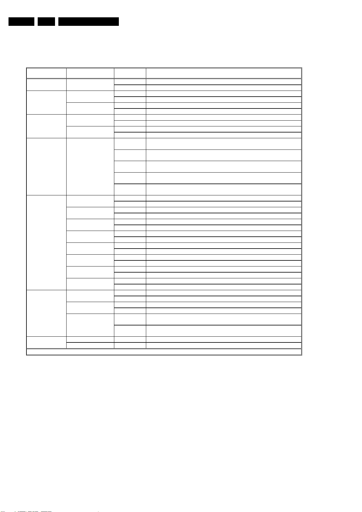
EN 84 F21RE AB8.
8.4.3 Service Options
Select this sub-menu to set the initialisation codes (= options)
of the set via text menu's.
Menu-item Subjects Options Description
Europe Setting for Europe Chassis region Region (for EU)
AP Setting for AP PAL-multi
Dual Screen
TXT/EPG Dual
Screen (for EU)
Teletext
NexTView (for EU)
Monitor type Monitor
Video repro
improvement
Signalling bits
Miscellaneous
Note:
Above overview gives the menu items for all regions (EU/AP/US). The correct settings differs per region (see Option Numbers).
(for EU)
(for EU)
Stand Alone
Group 1 e.g. 04492 08449 49555 04112 (see sticker on bottom receiver-box) Opt. No.
Group 2 e.g. 04151 00000 00000 00257 (see sticker on bottom receiver-box)
Yes Feature present PIP/Dual Screen
No Feature not present
Yes Feature present
No Feature not present
Yes Flash RAM present Flash RAM (for EU)
No Flash RAM not present
2 EPG level 2 setting
2C3 EPG level 3 setting
F19 Receiver-box can operate with 42î F19D-monitor, when jumper settings on
FM23 Receiver-box can operate with 32î FM23-monitor, when jumper settings
FM24 (SL) Receiver-box can operate with 42î FM24-monitor, when jumper settings
FM25-SL Receiver-box can operate with 50î FM25-monitor, when jumper settings
FM26 (SL) Receiver-box can operate with 42î FM26-monitor, when jumper settings
Eagle Eagle present (Pixel Plus) Featurebox type
Falconic Eagle not present (no Pixel Plus)
Yes Feature present Light sensor
No Feature not present (for FTV1.9 and FM25-SL monitors only)
Yes Feature present 2D Combfilter
No Feature not present
Yes Feature present (for US only) 3D Combfilter
No Feature not present
Yes LTP (TOPIC) present Picture
No LTP (TOPIC) not present
Yes Feature present Auto scavem
No Feature not present
Yes Feature (Eagle) present Pixel Plus
No Feature (Eagle) not present
Yes For 16:9 sets
No For 4:3 sets
Yes Set with Home Cinema link Home Cinema
No Set without Home Cinema link
Yes Feature present Integrated Cinema
No Feature not present
Yes Option needed for Service to be able to service the receiver-box with a
No Default setting. In this setting, the receiver-box will go to Standby when
Electrical Alignments
AVI-panel are configured in 1.9-mode
on AVI-panel are configured in 2.3-mode
on AVI-panel are configured in 2.3-mode (SL= Speaker Less)
on AVI-panel are configured in 2.3-mode (SL= Speaker Less)
on AVI-panel are configured in 2.3-mode (SL= Speaker Less)
normal PC monitor
connected to PC monitor
CL 36532021_015.eps
310303
8.4.4 Option Numbers
Select this sub-menu to set all options at once (expressed in
two long numbers).
An option number (or 'option byte') represents a number of
different options. When you change these numbers directly,
you can set all options very fast. All options are controlled via
eight option numbers.
Example: The sticker on the bottom cover of an E-box gives
the following option numbers:
04556 00257 49411 04112
04119 00001 00000 00271
The first line (group 1) indicates options 1 to 4, the second line
(group 2) options 5 to 8 (see tables below).
Figure 8-4 Service options overview
Every 5-digit number represents 16 bits (so maximum number
can be 65536 if all options are set).
When all the correct options are set, the sum of the decimal
values of each Option Byte (OB) will give the option number.
Page 85
Electrical Alignments
EN 85F21RE AB 8.
OB Bit Option name Settings (in decimal values) for F21RE_AB chassis Option
number
Featurebox 0= None
0
1
2
2= Prozonic
3= Eagle
4= Falconic (fixed)
5= Falconic 1050i 1250i
3 Comb Filter 0= Off 8= On (fixed)
4 Auto-Scavem 0= Off (fixed) 16= On (not appl. for FTV)
5 n.a. * 0
6 Light Sensor 0= Off (for FTV1.9 and FM25) 64= On (for the rest)
7 Luma Trans. Proc. 0= Off (for Eagle - PixelPlus - sets) 128= On (for non-Eagle sets)
1
8 PICNIC 0= Off 256= On (fixed)
Sum OB1
(decimal)
9 n.a. * 0
10 n.a. * 0
11 LNA 0= Off (fixed) 2048= On (not appl. for FTV)
12 WSS 0= Off 4096= On (fixed)
13 3D Comb Filter 0= Off 8192= On (fixed)
14 n.a. * 0
15 n.a. * 0
0 Headphone 0= Off 1= On (fixed)
1 Dolby ProLogic 0= Off (fixed) 2= On (not appl. for FTV)
2 Virtual Rear Spkrs 0= Off (fixed) 4= On (not appl. for FTV)
3 Cordless Rear Spkrs 0= Off (fixed) 8= On (not appl. for FTV)
4 Dolby Digital 0= Off (fixed) 16= On (not appl. for FTV)
5 DAS Cabinet 0= Off (fixed) 32= On (not appl. for FTV)
6
Subwoofer 0= Off (fixed)
7
2
8 P50 (for EU) 0= Off (fixed) 256= On
64= Type 1 (not appl. for FTV)
128= Type 2 (not appl. for FTV)
Sum OB2
(decimal)
9 n.a. * 0
10 n.a. * 0
11 n.a. * 0
12 EPG Item (for EU) 0= Off (fixed) 4096= On
13 EPG Type (for EU) 0= Off (fixed) 8192= On
14 n.a. * 0
15 n.a. * 0
0 AV3 0= Off 1= On (fixed)
1 AV4 0= Off 2= On (fixed)
2 AV4 (2fH) 0= Off (fixed) 4= On
3 n.a. * 0
4 Dual Screen 0= Off (fixed) 16= On
5 Scaler 0= Off (fixed) 32= On
6 EPG/TXT DS (for EU) 0= Off (fixed) 64= On (not for US)
7 Aux. Headphone 0= Off 128= On (fixed)
3
8 Aspect Ratio 0= 4:3 (not appl. for FTV) 256= 16:9 (fixed)
Sum OB3
(decimal)
9 Tilt 0= Off (fixed) 512= On (not appl. for FTV)
10 DAF 0= Off (fixed) 1024= On (not appl. for FTV)
11 One Point Control 0= Off (fixed) 2048= On (not appl. for FTV)
12 Stand Alone 0= Off (with Philips plasma monitor) 4096= On (with standard PC-monit.)
13 200 Presets 0= Off (fixed) 8192= On (not appl. for FTV)
14 Home Cinema 0= Off 16384= On (fixed)
15 Integrated RC (P50) 0= Off 32768= On (fixed)
MSP 0= MSP3415 (fixed) 1= MSP3451 (not appl. for FTV)
0
1
2= MSP3411 (not appl. for FTV)
2 China IF 0= Off (fixed) 4= On
3 Tuner 0= Philips (default) 8= Alps (optional)
4 Teletext 0= Off 16= On
5 China Teletext 0= Off (fixed) 32= On
6 Closed Caption 0= Off (fixed) 64= On (not for EU)
7 n.a. * 0
4
8 Digital Module (MILO) 0= Off (fixed) 256= On (not appl. for FTV)
Sum OB4
(decimal)
9 n.a. * 0
10 n.a. * 0
11 n.a. * 0
12 Anti Aging mode 0= Off 4096= On
13 n.a. * 0
14 n.a. * 0
15 n.a. * 0
*) Note:
Bits that are not used have a fixed value of "0", and are mentioned as "n.a. *" in above overview.
CL 36532021_023.eps
030403
Figure 8-5 Option bytes Group 1
Page 86
EN 86 F21RE AB8.
Electrical Alignments
OB Bit Option name Settings (in decimal values) for F21RE_AB chassis Option
0 Auto TV mode 0= Off 1= On
1
Auto Store Mode 0= None
2
3 n.a. * 0
4 Picture Mute 0= Off 16= On
5 Demo mode 0= Off 32= On
6 Virgin mode 0= Off 64= On
5
7 n.a. * 0
8 n.a. * 0
9 n.a. * 0
10 n.a. * 0
11 n.a. * 0
12 TXT Preference 0= TOP 4096= FLOF
13 n.a. * 0
14 n.a. * 0
15 n.a. * 0
0 P50 DVD menu-line 0= Off 1= On
1 Asia 0= Off 2= On
2 n.a. * 0
3 n.a. * 0
4 n.a. * 0
5 n.a. * 0
6 n.a. * 0
7 n.a. * 0
6
8 n.a. * 0
9 n.a. * 0
10 n.a. * 0
11 n.a. * 0
12 n.a. * 0
13 n.a. * 0
14 n.a. * 0
15 n.a. * 0
0 n.a. * 0
1 n.a. * 0
2 n.a. * 0
3 n.a. * 0
4 n.a. * 0
5 n.a. * 0
6 n.a. * 0
7 n.a. * 0
7
8 n.a. * 0
9 n.a. * 0
10 n.a. * 0
11 n.a. * 0
12 n.a. * 0
13 n.a. * 0
14 n.a. * 0
15 n.a. * 0
Cabinet 0= (not appl. for FTV)
0
1
2
3
4 SLDP 0= Off (fixed) 16= On (not appl. for FTV)
5 n.a. * 0
6 AVL 0= Off (fixed) 64= On
7 n.a. * 0
8
*) Note:
FTV Monitor
8
(auto detect)
9
10
11
12
13
14
15
Bits that are not used have a fixed value of "0", and are mentioned as "n.a. *" in above overview.
0= FTV1.9
2= PDC/VPS
4= TXT Page
6= PDC/VPS/TXT Page
1 - 14= (not appl. for FTV)
15= Other (fixed)
256= FM23 (default)
512= FM24
768= FM24-SL
1024= FM25-SL
1280= FM26
1536= FM26-SL
1792= FM27
2048= FM27-SL
65280= Other
Number
Sum OB5
(decimal)
Sum OB6
(decimal)
Sum OB7
(decimal)
Sum OB8
(decimal)
CL 36532021_024.eps
030403
Figure 8-6 Option bytes Group 2
Note: If the EAROM is replaced, all the options will require re-
setting. To be certain that the factory settings are reproduced
exactly, you must set both option number lines. These numbers
can be found on the bottom of the Receiver box.
Page 87
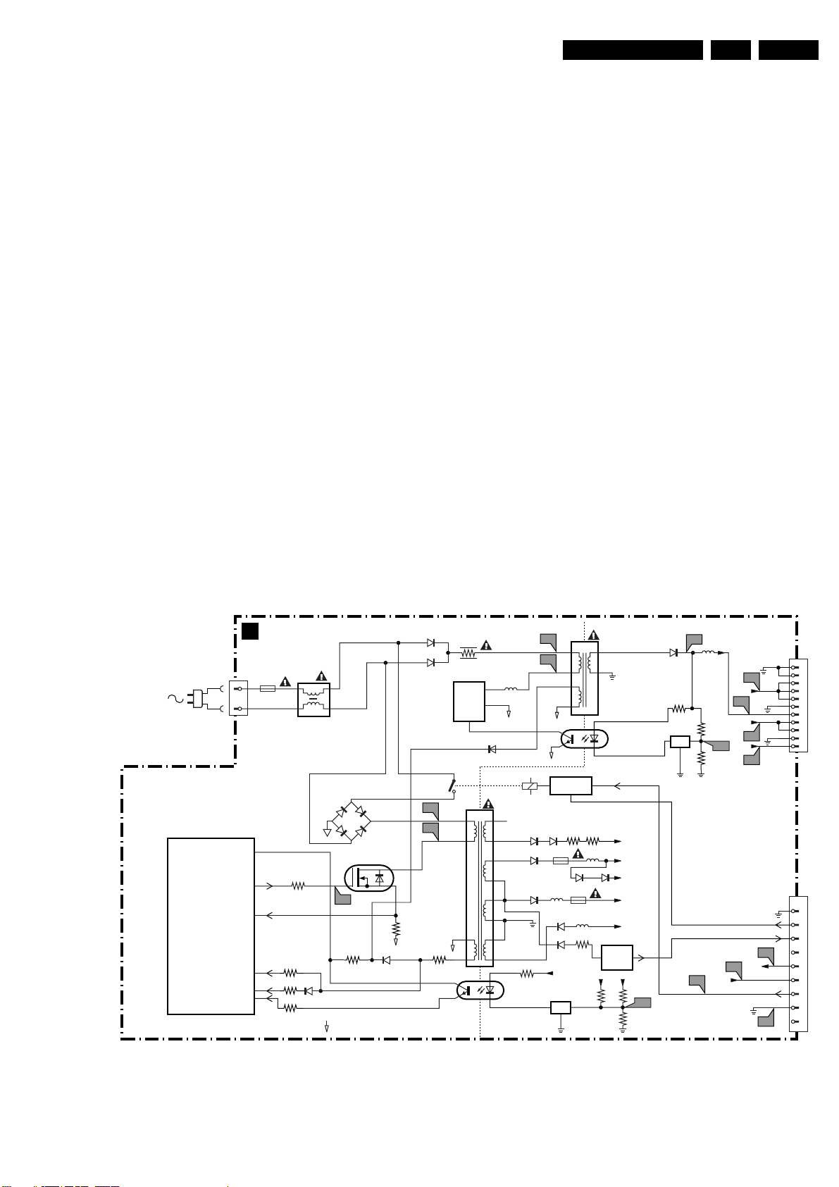
Circuit Descriptions, List of Abbreviations, and IC Data Sheets
EN 87F21RE AB 9.
9. Circuit Descriptions, List of Abbreviations, and IC Data Sheets
Index of this chapter:
1. Introduction
2. Power Supply Unit (PSU)
3. Audio Video Interface panel (AVI)
4. Small Signal Panel (SSP)
5. Front panel (FP)
6. Auto TV
7. Abbreviations
8. IC Data sheets
Note:
• Figures can deviate slightly from the actual product, due to
different set designs.
• For a good understanding of the following circuit
descriptions, please use the diagrams in chapter 6 and 7.
Where necessary, you will find a separate drawing for
clarification.
9.1 Introduction
This Receiver box (or E-box) is developed for the global
market. The service chassis name is F21Rx (x stands for the
region; e.g. E=Europe, U= USA). It is an economic version of
the F22Rx chassis, with the following features:
• Feature Box 7 for better EMC behaviour and improved
"Natural Motion", however without "Eagle" (Pixel Plus).
• Without "Double Window" panel.
• Improved Tuner/Splitter (less noise).
• Without "Down Scaler" panel.
It can drive both FTV1.9 and FM2x plasma screens.
9.2 Power Supply Unit (PSU, diagram PS)
9.2.1 PSU: Introduction
A 35W Power Supply is used in the Receiver box. It supports a
range of input voltages (= global), and can be used for almost
every E-box version. It delivers the voltages for the SSP, the
DW, the FBX (+5VSTB, 5V2, 8V6, 7V7, -7V7 and 33V), and for
the specific PWBs. The output of the power supply is
connected to the AVI panel. This panel powers all the other
PWBs.
The Mains voltage is applied to the input filter that feeds it to the
standby supply. This supply is always operational and delivers
the +5VSTBY voltage.
The task of the main supply is to deliver the supply voltages for
the several electrical circuits in the Receiver box. It is switched
via a single-pole relay, which is powered from the +5VSTBY
voltage and controlled via the POWER_ON and STANDBY
signals.
The reason to choose for a separate standby supply, instead of
a single flyback supply (which can be driven in standby mode
like a MC44604), is the requirement to have very low standby
power consumption.
The "POWER ON/STBY" knob is located on the Front I/O panel
and activates the relay supply (POWER_ON). The
microprocessor is then able to switch the set from "standby" to
"on" (STANDBY).
The green "POWER ON" LED is active, when the 8.6 V is
present (HW controlled).
The red "STANDBY" LED is active in standby. The OTC
controls this via ON_OFF_LED.
150 - 250V
7001
MC44603A
CONTROL
OUTPUT
CURRENT SENSE
OVERVOLTAGE PROTECTION
VOLTAGE FEEDBACK
POWER SUPPLY STANDBY SUPPLY
0300
1
2
VCC
Vdem IN
PS
1
3
7
8
6
14
T2,5A
1001
3030
3041
3037
5000
MAIN SUPPLY
6000
3
GBU4J
1
3042
6009
4
6000
2
STP6NC60
G
F013
3016 6007
HOT GROUND HOT COLD
6203
6204
7200
TNY256
CONTROL
2
3
F008
F011
D
S
3012
3013
3014
3015
3200
DRAIN
SOURCE
ENABLE
5003
3
4
6
8
5
4
STANDBY
31103111
F026
3113
3114
6310
SB340
7202
TL431
3310
REF.
2
F067
81
F056
+5VSTBY
5300
3312
F069
3313
3314
POWER-ON
POWER-VALID
-7V7
STANDBY
F054
+5V2
F038
+8V6
+33V
F032
F042
F044
+7V7
F052
F058
0307
1
2
3
4
5
6
7
8
9
10
11
0306
1
2
3
4
N.C.
5
6
7
8
9
N.C.
5200
F072
F073
5202
5
2.3
4
6010
7401, 7402
1
ACTIVATING
CIRCUIT
2
16
N.C.
6101 6110 3101 3102
15
6103
3109
6106
5103
6107
6108
+8V6
7011
TL431
REF.
1101
T4A
1
2
14
13
12
11
10
9
7002
TCET1103
2
1
4
3
5
4
2
5102
6104 6105
1102
T4A
5104
3107
+8V6
81
7
8
1
2
7101
7203
TCET1102
POWER
VALID
CIRCUIT
+5V2
+33V
+8V6
+7V7
+5V2
-7V7
Figure 9-1 Block Diagram Power Supply
CL 16532098_003.EPS
150801
Page 88
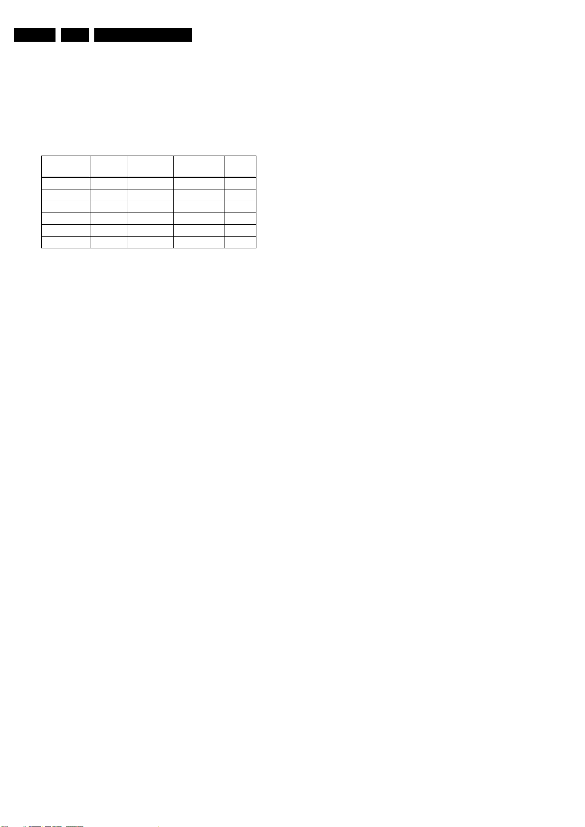
EN 88 F21RE AB9.
Circuit Descriptions, List of Abbreviations, and IC Data Sheets
The Power Supply module consists of three parts:
1. Mains voltage inlet and filter.
2. Standby supply.
3. Main supply.
The total power balance of the supply can be read from the
following table:
Table 9-1 Total power balance
Supply Value
(V)
5V2 5.2 3 2.0 13
8V6 8.6 7 1.25 13.8
+7.7V_audio 8.6 7 0.1 1.2
-7.7V_audio -5.2 7 0.1 1.2
33V_tuner 33 4 mA max. 0.1
5VSTB 5.32 5 0.3 2.7
9.2.2 PSU: Start-up Sequence
For a description of the "start-up sequence", we make a
differentiation between the FTV1.9 and the FM2x monitors.
Start-up sequence for an E-box + FTV1.9 Monitor
There are five different "power states" in the E-box:
• Low Power Standby (P < 0.9 W). The Main supply is not
working. Only the OTC and I/O Expanders (on the AVIpanel) are powered from the 5VSTB. The OTC works in
one of the low power states (no program execution, but the
UART, timer, RC pre-processor, and SW ADC are
working).
• Standby (P < 3 W). The Main supply is not working. Only
the OTC and I/O Expanders (on the AVI-panel) are
powered from the 5VSTB. The OTC works in high power
state (= normal).
• Semi Standby (Europe only). The Main supply is working.
All PWBs are powered. The video in the HOP and the audio
on the AVI board are muted. The sync is not send to the
monitor. This state is used for EPG and P50 operations.
• On (P < 35 W). The Main supply is working. All PWBs are
powered.
• Off. The OTC and I/O Expanders are not powered
anymore. All the voltages are "off".
The E-box will always start-up in the "Standby" state until the
CONFIG_IDENT is detected (means monitor attached). During
initialisation, the E-box must check the "TV_standby" bit in the
NVM, to decide into which state the E-box and monitor have to
be put. This will set the STANDBY pin on the OTC accordingly.
The initialisation starts when the E-box is switched "on" and the
AC-power is connected. As a result, the 5VSTB supply is
activated, and the OTC is activated. Now, the OTC checks the
presence of the CONFIG_IDENT signal:
• If this check is successful (this means two following "hand
shake" sequences are detected), then the state of the Ebox depends on the "TV_standby" bit in the NVM. This bit
contains the history data about how previously the TV
configuration entered the "standby" state (e.g. when this
was done by the user (bit= 1), the set will stay in "standby").
• If this check is not successful, the E-box will go to "Low
Power Standby".
Note: For service, the E-box can work in "Stand-alone" power
mode. This is detected via the "Stand alone" bit in the NVM.
This bit can be set in the Dealer/Service menu.
If the E-box is switched from "Standby" to "On", the STANDBY
pin of the OTC is pulled "low", the relay switch is closed, and
the main supply is started up. When the 5V2 and 8V6 voltages
reach their nominal values, the 5V2_PROT and 8V6_PROT
are activated. Now:
Tolerance
(%)
Typ. Current
(A)
P_max
(W)
1. The MSP shall be reset first, as this IC can disturb the I2C
traffic, when not reset properly.
2. Secondly, as the POPOV IC of the DW (F2R22 only) can
pull the slow SDA line "low" when the HA signal from the
main HIP is not available, all traffic on the slow I2C bus
needs to be delayed until the HIP is properly initialised and
settled. This means a wait state of 100 ms, after the crystal
configuration of the HIP has correctly been read out.
3. Next, all other ICs are initialised. Now, the E-box is
working, but the monitor is still not displaying a picture.
4. The HOP switches on the PHI1 loop, the software sets all
the necessary video and audio parameters, and enables
them.
Start-up sequence for an E-box + FM2x Monitor
There are five different "power states" in the E-box:
• Low Power Standby (P < 0.9 W). The Main supply is not
working. Only the OTC, I/O Expanders (on the AVI-panel)
and remote circuits are powered from the 5VSTB. The
OTC works in one of the low power states (no program
execution, but the UART, timer, RC pre-processor, and SW
ADC are working).
• Peripheral Standby (P < 3 W). This is an intermediate
state. This mode is only used temporarily, if the OTC goes
from low power standby to normal operation and vice
versa.
• Semi Standby (Europe only). The Main supply is working.
All PWBs are powered. The video in the HOP and the audio
on the AVI board are muted. The sync is not send to the
monitor. This state is used for EPG and P50 operations.
• On (P < 35 W). The Main supply is working. All PWBs are
powered.
• Off. The OTC and I/O Expanders are not powered
anymore. All the voltages are "off".
The E-box will always start-up in the "Standby" state until the
AYT (Are You There) is detected. This means that an FM2x
monitor is attached (this is different from the FTV1.9 monitor,
where a separate CONFIG_IDENT line is used). During
initialisation, the E-box must check the "Stand_alone" bit in the
NVM. If this bit and the "TV_standby" bit both are not set, the
AYT protocol is started, and will wake up the monitor. This will
set the STANDBY pin on the OTC accordingly.
The initialisation starts when the E-box is switched "on" and the
AC-power is connected. As a result, the 5VSTB supply is
activated, and the OTC is activated. Now, the OTC checks the
presence of the "Standby" bit:
• If the "Standby" bit and the "Stand_alone" (or "Service/
Factory") bit are not set, the AYT protocol is enabled,
which will wake up the monitor. If this check is successful,
the state of the E-box depends on the "TV_standby" bit in
the NVM. This bit contains the history data about how
previously the TV configuration entered the "standby" state
(e.g. when this was done by the user (bit= 1), the set will
stay in "standby").
• If this check is not successful (e.g. set to standby by user),
the E-box will go to "Low Power Standby".
Note: For service, the E-box can work in "Stand-alone" power
mode. This is detected via the "Stand alone" bit in the NVM.
This bit can be set in the Dealer/Service menu. If this bit is
"high", the AYT protocol is not used and no FSP commands are
send to the monitor.
If the E-box is switched from "Low Power Standby" to "On", the
STANDBY pin of the OTC is pulled "low", the relay switch is
closed, and the main supply is started up. When the 5V2 and
8V6 voltages reach their nominal values, the 5V2_PROT and
8V6_PROT are activated. Now:
1. The MSP shall be reset first, as this IC can disturb the I2C
traffic, when not reset properly.
2. Secondly, as the POPOV IC of the DW (F22Rx only) can
pull the slow SDA line "low" when the HA signal from the
main HIP is not available, all traffic on the slow I2C bus
needs to be delayed until the HIP is properly initialised and
Page 89
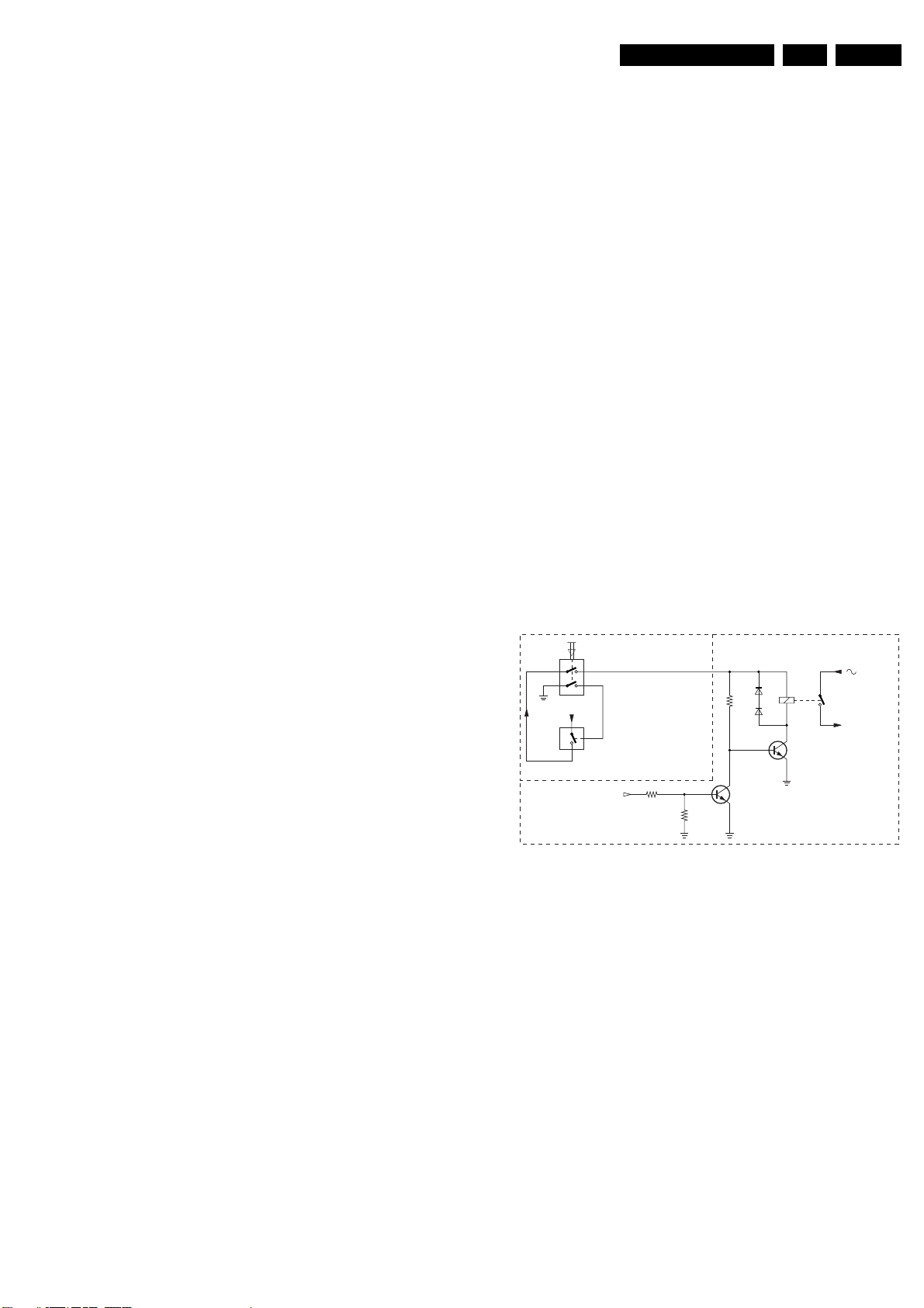
Circuit Descriptions, List of Abbreviations, and IC Data Sheets
EN 89F21RE AB 9.
settled. This means a wait state of 100 ms, after the crystal
configuration of the HIP has correctly been read out.
3. Next, all other ICs are initialised. Now, the E-box is
working, but the monitor is still not displaying a picture.
4. The HOP switches on the PHI1 loop, the software sets all
the necessary video and audio parameters, and enables
them.
9.2.3 PSU: Mains Voltage Inlet and Filter
The Mains voltage is provided by inlet 0300, after which it is
fused by a T2.5A fuse. The next part, the Mains voltage filter,
consists of an LC-common mode filter section. This filter
consists of two capacitors (items 2002 and 2004) from both
phase and neutral to ground (to reduce the leakage current)
and an inductor (5000). Interferences on one of the phases are
shorted to ground by these capacitors.
Inductor 5000 also provides a differential-mode filtering with
capacitor 2001. Resistor 3003 discharges this capacitor after
the Mains voltage is disconnected.
At high voltage peaks (for example, lightning surges) on one of
the phases, the resistance of VDR 3002 will be very low,
causing fuse 1001 to interrupt. At a lightning surge on both
phases with respect to chassis ground, the Mains voltage filter
will form a high resistance, through which the voltage will rise
very sharply. To prevent flashovers, a spark gap (item 1000) is
implemented.
Resistors 3000 and 3001 are connected between neutral and
chassis ground. They are required by safety regulations.
9.2.4 PSU: Standby supply
Start up
The Standby Supply operates on the AC voltage from the input
filter part, and has to deliver a stable regulated 5 V value. The
standby supply is always operational when the AC input
voltage is present, even when the POWER switch is in the "off"
position.
After a small bridge rectifier and buffer capacitor (D6203/6204
and C2202), the DC voltage is applied to a switched mode
power supply. To reduce self-pollution, the rectifiers are
bridged by small capacitors (C2200/2201).
Normal Operation
The Standby Supply itself is build around a "TINYSwitch"
TNY256. This IC contains the control circuitry and a power
MOSFET needed for an Switched Mode Power Supply
(SPMS). It uses a simple "on/off" control loop to regulate the
output voltage.
The supply for the TNY256 comes via safety resistor R3200,
L5200, and L5202.
The +5VSTBY voltage at the secondary side is rectified by
D6310 and smoothed by C2311.
By using secondary sensing, a very accurate +5VSTBY
voltage and high efficiency is achieved. The sensing circuit
uses a TL431 as reference voltage/error amplifier. Optocoupler
7203 and coil 5200 are used for the Mains voltage isolation.
When the +5VSTBY output voltage rises, the reference voltage
on the TL431 will exceed 2.5 V and the current through this
device and the optocoupler LED will increase. By this method,
the optocoupler transistor will conduct more. When this current
(at pin 4 of IC7200) exceeds 50 µA, the MOSFET is switched
"off", and the output voltage will drop. When the current drops
below 40 µA, the MOSFET is switched "on" again.
Output Voltage
+5VSTBY, which is available on connector 0307, pin 7.
Protections
As the TNY256 is sensitive for transients, a "peak clamp" circuit
(300 V zener diodes 6201 and 6202) is used to limit the voltage
to a safe level.
9.2.5 PSU: Main supply
Introduction
The main supply is activated by single-pole relay 1400, which
delivers the filtered Mains voltage to a rectifier bridge (item
6000). This rectified voltage is the input for the flyback
converter, which generates the output voltages.
The flyback converter is based on a MC44603AP driven in
"discontinues conduction mode" with a fixed frequency of 40
kHz (at nominal Mains voltages). The MC44603AP drives a
MOSFET (600 V, 1.2 Ohm), which is snubbered (by 2008) and
clamped by an RCD peak clamp. The transformer delivers the
secondary output voltages and the primary supply voltage for
the IC.
Secondary voltage control is on the 5V2 and 8V6 output via a
TL431 (item 7011) and an optocoupler (item 7002) back to the
error amplifier input of the controller IC.
Output Voltages
The following voltages are generated by the main supply:
• +33V (0307/11) for the Tuner.
• +16V (0306/9).
• +8V6 (0307/8 & 9).
• +7V7 (0306/5).
• -7V7 (0306/6).
• +5V2 (0307/4 & 5).
• +5V2_FB (0307/3).
Start up
ON/OFF
FP PS
3
6
+5VSTBY
7055
+5VSTB
1006
2/3
8/7/6
2/1
5/4
4
STANDBY
(FROM µP)
POWER-ON
3402
3403
7402
3401
6401
6402
1400
7401
Figure 9-2 Start up circuitry
The mechanical "on/off" switch (item 1006) on the Front panel
drives IC7055. This is a "power distribution switch", used due
to the high switch-on current. It has internal overload and shortcircuit protections.
A single pole 5 V relay (item 1400) will switch the Receiver box
from "standby" to "on". It is controlled via the POWER_ON line.
The start up supply voltage of the control IC comes via the
standby supply. It is rectified (D6010), smoothed (C2025), and
clamped (D6008). Once the main supply is started, this voltage
is taken over by winding 6-8 of transformer 5003 and diode
D6007.
Normal operation
The working frequency of 40 kHz is determined by R3032 and
C2014. The output voltage is controlled by duty cycle
regulation. Output is on pin 3, which drives the FET. A current
will flow through transformer coil 3-4 (item 5003), FET 7000,
and sense-resistors R3012//R3013//R3014 to ground. The
energy stored in the primary winding during the on time is
delivered to the secondary windings during the "off" time.
The output voltages are rectified and buffered here.
2
3
CL36532021_001.eps
TO BRIDGE
RECTIFIER (6000)
180303
Page 90
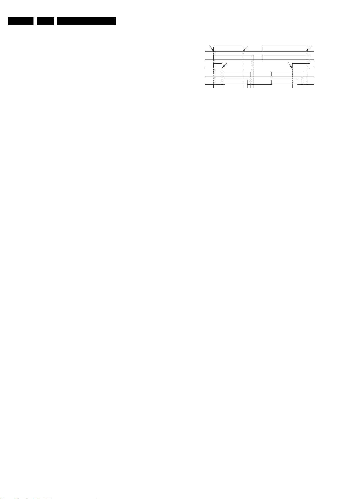
EN 90 F21RE AB9.
Circuit Descriptions, List of Abbreviations, and IC Data Sheets
Regulation is performed by the control loop that consists of
reference component 7011 and optocoupler 7002. When the
+5V2 output voltage rises, the reference voltage on the TL431
will exceed 2.5 V and the current through this device and the
optocoupler LED will increase. By this method, the optocoupler
transistor will conduct more, and the voltage over R3035 (and
pin 14 of IC7001) will rise. The IC will adjust the duty cycle, the
FET will conduct less, and the output voltage will decrease.
Protections
Soft Start and Maximum Duty Cycle
The output voltage is 0 V at start up. This would force IC 7001
to start with a maximum duty cycle, causing a very high current
through FET 7000. To prevent this, capacitor C2018 (at pin 11
of IC7001) ensures a soft start (voltage at pin 11 is low at start
up, which gives a small duty cycle) and R3039 determines the
maximum duty cycle.
Switch Off Peak Voltage
To protect the FET against high peak (drain-source) voltages
at switch "off", a peak clamp circuit is added consisting of
D6014, D6002, C2007, and R3010.
When the FET blocks, the diodes will lead the peak voltages
away from the FET and will charge C2007.
When the FET conducts, this capacitor is discharged via
R3010, the primary coil, and the FET itself.
Over Current and Fold Back
The current through the primary winding is measured by sense
resistors R3012, R3013, and R3014. The resulting voltage is
measured at pin 7 of IC7001. Once the voltage at this pin
exceeds 1 V (so maximum current is set to 3 A), the duty cycle
is regulated back.
If the output load keeps on increasing (I > 3 A), the system is
unable to supply enough energy to maintain the output voltage
in regulation. This is detected at pin 5 of IC7001 (via pin 8 of
5003, R3015, D6007 and R3037). Consequently, if this voltage
drops below the fold back threshold voltage of 1 V, the IC will
adapt the "current sense threshold". This will limit the current
supply and by this, the output voltage. This will cause an
avalanche effect, causing the supply to rapidly trim down.
Over Voltage
When the voltage on pin 6 of IC7001 will exceed 2.5 V, the
control IC will stop oscillating (after 2 µs). The output voltages
will drop, and the IC starts again. This can happen when the
feedback loop is interrupted.
Switch On/Off Behaviour
Mainsplug In
Umains
5Vstby
Standby
33V, 8V6, 7V7, 5V2, -7V7
Power_valid
t0
= Mainsplug In.
t1
= From STANDBY to ON.
= Mainsdip
t3
= From ON to STANDBY
t7
= Mainsplug Out
t10
STBY to ON
t0
t6 t10t9t8t7t5t4t3t2t1
ON to STBY
Figure 9-3 Timing diagram Power Supply
The start up of the PSU has to fulfil certain requirements.
At the moment the Mains cord is connected (t0), the standby
supply will generate the +5VSTBY (coming from the STANDBY
pre-condition). With this voltage present, the microprocessor
begins the start up procedure, by making the STANDBY
command logic "low" (t1) and the POWER_ON command
"high" (coming from the "off" pre-condition). After you press the
power switch on the front panel, the "POWER_ON" signal will
become "high" and within 2 seconds, the main supply will start,
making the POWER_VALID signal "high" (t2).
When a Mains dip occurs (t3), the POWER_VALID signal must
go "low" before the output voltages will drop and must remain
"low" until the Mains voltage returns.
When you put the set in standby, the microprocessor makes
the STANDBY signal "high" (t7). The output voltages will drop,
and the POWER_VALID signal goes "low", but the +5VSTDBY
remains present.
Finally, this voltage will drop when the Mains cord is
disconnected (t10).
Typical timing values are:
• t1 - t2 = 0.1 < t < 1.2 s (dependent on the STANDBY PSU
load).
• t3 - t4 = 20 < t < 350 ms (dependent on U_MAINS).
• t4 - t5 = 5 < t < 40 ms (dependent on the main PSU load).
• t5 - t6 = 10 < t < 1000 ms (dependent on U_MAINS and the
STANDBY PSU load).
• t7 - t8 = 10 < t < 600 ms (dependent on U_MAINS and the
MAIN PSU load).
• t8 - t9 = 5 < t < 40 ms (dependent on the MAIN PSU load).
Mainsplug OutMains Dip
CL16532098_002.eps
240901
Demagnetisation
The internal demagnetisation block in IC7001 disables the
output (pin 3) during the demagnetisation phase of transformer
5003. This is to prevent the FET from being switched "on". The
info is taken from pin 8 of transformer 5003, and fed via R3015
and R3030 to pin 8 of IC7001. When the voltage on this pin
drops below 65 mV, the demagnetisation phase is completed,
and the FET can switch on.
Audio Plop
The POWER_VALID circuit is designed to detect the
disappearance of the Mains voltage (at set switch "off" or at
Mains voltage dips). This signal will then mute the audio
outputs to prevent audio plops (see diagram AV8 position I7).
The circuit compares the +5V2 output with the negative
rectified 5V2 winding (which is in fact the transformed rectified
Mains voltage). When this voltage disappears, transistor 7101
is activated and the POWER_VALID output will go "low" before
the supply output voltages will drop. It will mute the audio
outputs and stay "low" until the Mains voltage and the +5V2
output voltage returns.
Page 91
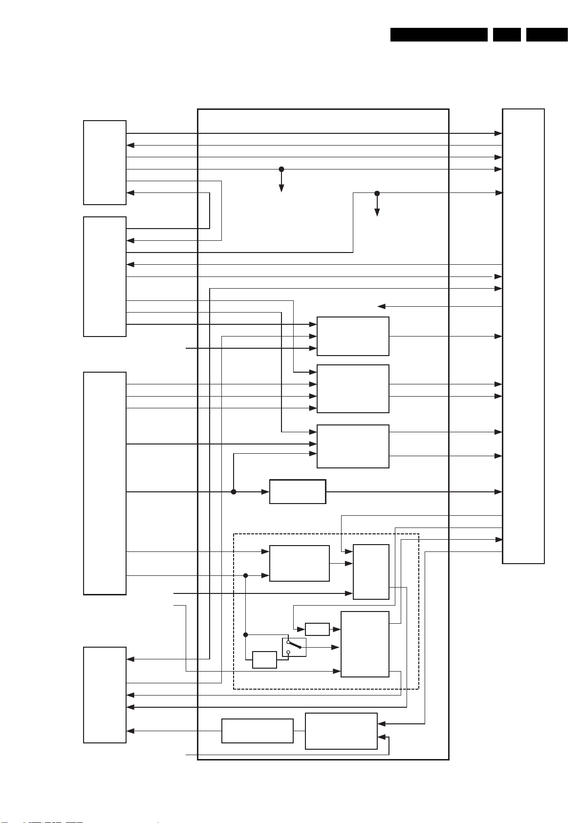
Circuit Descriptions, List of Abbreviations, and IC Data Sheets
9.3 Audio Video Interface Panel (AVI, diagram AV)
9.3.1 AVI: Introduction
EN 91F21RE AB 9.
POWER
SU
PPLY
FRONT
PANEL
POWER_VALID/
50HZ_60HZ
STANDBY
+16V/+7V7/-7V7/+33V
+5V2/+8V6
+5VSTBY
POWER_ON
POWER_ON
+5VSTBY
+5VSTB
IR_LED/ON_OFF_LED
KEYBOARD
SND_FRONT
CVBS_YC_FRONT
RC_FRONT
RC_EXT
SND_SD
SND_EXT3
SND_HD
AVI
+5V2/+8V6
+5VSTB
I2C
RC SELECTION
AUDIO
SELECTION
POWER_VALID/
50HZ_60HZ
STANDBY
+5V2/+8V6
+5VSTB
IR_LED/
ON_OFF_LED
KEYBOARD
UART
I2C
RC_OUT
SND_MAIN
SND_SUB
SSP
HD
PANEL
FTV1.9/2.X
MONITOR
CVBS_YC_EXT3
YPBPR_SD
HV_EXT_HD
RGB_YPBPR_HD
HV_VGA
RGB_VGA
UAR
T
RC_MON
RGB_MON
HV_MON
YPbPr to RGB
HD
SYNC
PROCESSING
LPF
MAT-
RIX
2fh video and sync processing
1FH VIDEO
SELECTION
SYNC
SELECT
2FH
2FH VIDEO
VIDEO
SELECTION
SELECTION
CVBS_YC_AV1
CVBS_YC_AV2
UI_RGB_FBL
HDVD
RGB_VC
RGB_HD
SND_SSP
2FH
SND_MON
SND_CENTER
AUDIO
MUTE
LEFT/RIGHT
CENTER
SELECTION
Figure 9-4 Block diagram AVI panel
CL 36532021_002.eps
180303
Page 92
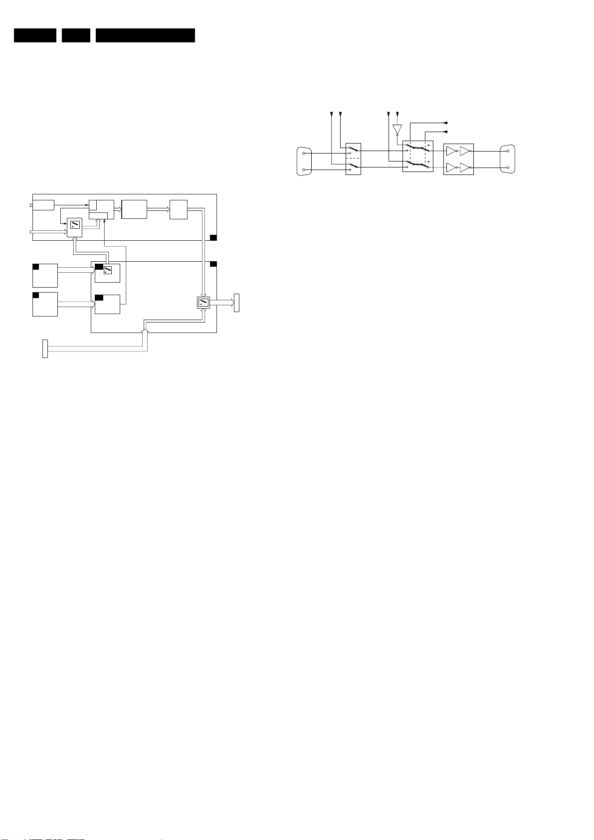
EN 92 F21RE AB9.
Circuit Descriptions, List of Abbreviations, and IC Data Sheets
The AVI contains a video switch, an audio switch, an I/O
expander, and an EPLD (or ACEX) with I2C control.
The AVI panel is an interface between the following panels/
sources:
• Small Signal panel (SSP).
• Front panel (FP).
• VGA input.
• Standard Definition panel (SD).
• Power Supply panel (PS).
It also contains the outputs to the plasma monitor.
9.3.2 AVI: Video Processing
RGB_VGA
RGB_VGA
730075011101
HOPFBXHIP
RGB_HD
INTERFACE
ANTENNA
SCART1
SCART2
CVBS/YC
SCART4
VGA
input
7208
CVBS/Y C
YPbPr 1fH
TEA 6415
CVBS_Y_AV1
& C_AV1
CVBS_Y_AV2
& C_AV2
IF
I/O
AV7
AV6
RGB-Fbl_1fH
YUVFbl_1fH_sc1_in
TEA 6415
YPbPr to
YUV (RGB)
Tuner
FP
frontpanel
SD
SD-
panel
SubD
15p
Figure 9-5 Block diagram video processing
1fH CVBS and YC Video Selection (diagram AV7)
For the video source selection, a TEA6415 (item 7710) from
SGS-Thomson is used. The main function of this IC is to switch
eight video input sources to six outputs. Each output can be
switched to only one of the inputs, but any same input may be
connected to several outputs. All the switching possibilities are
controlled through the I2C bus.
At the input of the IC, we find the following signals:
• CVBS or Y/C from FRONT.
• CVBS or Y/C from EXT3.
• CVBS or Y/C from the Scaler (not used in this chassis).
At the output of the IC we find:
• CVBS_Y_AV1 and C_AV1.
• CVBS_Y_AV2 and C_AV2.
AV1 is connected to the CVBS/YC_FRONT input of the SSP
(connector 0333).
AV2 is connected to the CVBS/YC_UI input of the SSP
(connector 0372).
These signals go to the SSP via connectors 0333 and 0372,
where they are fed to a second TEA6415 (item 7208), together
with the video signals coming from the SCART connectors.
1fH Video processing (diagram AV6)
The YPbPr signals coming from the SD panel (EXT5) are
buffered, and then fed through a YPbPr-to-RGB matrix circuit
(TSH93, item 7607). The matrix is made with discrete hardware
and determined by resistor values.
The RGB_SD output signals are then fed to connector 0372
and routed, via an RGB selector, to the RGB2 (Universal
Interface) input of the HIP IC (item 7501) on the SSP.
SSP
K
RGB_VC
AV
AV
SubD
15p
TO PDP
RGB_MON
MONITOR
VGA
OUTPUT
CL36532030_013.eps
030403
9.3.3 AVI: Sync Processing
General
V_HD
VGAin
H
V
H_HD
(N.C. for Europe)
H_VGA
V_VGA
7450
H_HD_VGA
V_HD_VGA
VD
(from SSP)
HD
HD_VGA-SELECT (from OTC)
7570
SYNC_TRISTATE_MON (from OTC)
7575
BUFFERS
Figure 9-6 Block diagram sync processing
The block diagram above shows the sync path. The AV
Interface has the following sync inputs:
• Sync from VGA source (HV_VGA)
• Sync from SSP (HD_VD)
The selection between these inputs for the main picture is done
with switch 7570. This switch is controlled via software with the
HD_VGA_SELECT signal.
Note: If the Receiver box has to function without the monitor
(e.g. in case of EPG data download), the H and V pulses may
not be fed to the monitor. In this case, switch 7570 will be put
open with the SYNC_TRISATE_MON control signal (SW
controlled).
9.3.4 AVI: Audio Processing
General
The audio-part of the AV-interface consists of three separate
parts:
• The source selection.
• The Channel-channel configuration.
• Muting (or anti-plop circuit).
Source Selection
The source selection part redirects the three stereo inputs into
two separate channels. These two channels (SNDL/
R_MAIN_OUT and SNDL/R_SUB_OUT) are then connected
to the SSP for further processing.
Note: The TEA6422 cannot handle the maximum level of 2.8 V
of the SNDL/R_VGA signals. Therefore, these signals are
attenuated by 3 dB (see R3801/3802 and R3806/3807 on
diagram AV8). All other inputs are attenuated at the Front I/O
panel or the HD connector panel. These attenuations are
corrected again on the SSP.
Centre Channel Selection
The Centre input (cinch at the rear) is a separate audio input.
This input bypasses all other inputs, and is designed to obtain
a better Home Cinema configuration. In this case, the FTV
monitor speakers will function as the centre channel. This input
is selected via the CENTER_SELECT signal, which is
controlled by the I/O Expander (items IC7880 and TS7853). It
is selected by the user from the user menu.
Mute
To prevent audio plops and clicks (when the set is turned "on/
off" or at channel switching), a mute circuit is implemented
immediately after the centre channel selection part.
H_MON
V_MON
CL 16532023_055.eps
VGAout
H
V
240901
Page 93
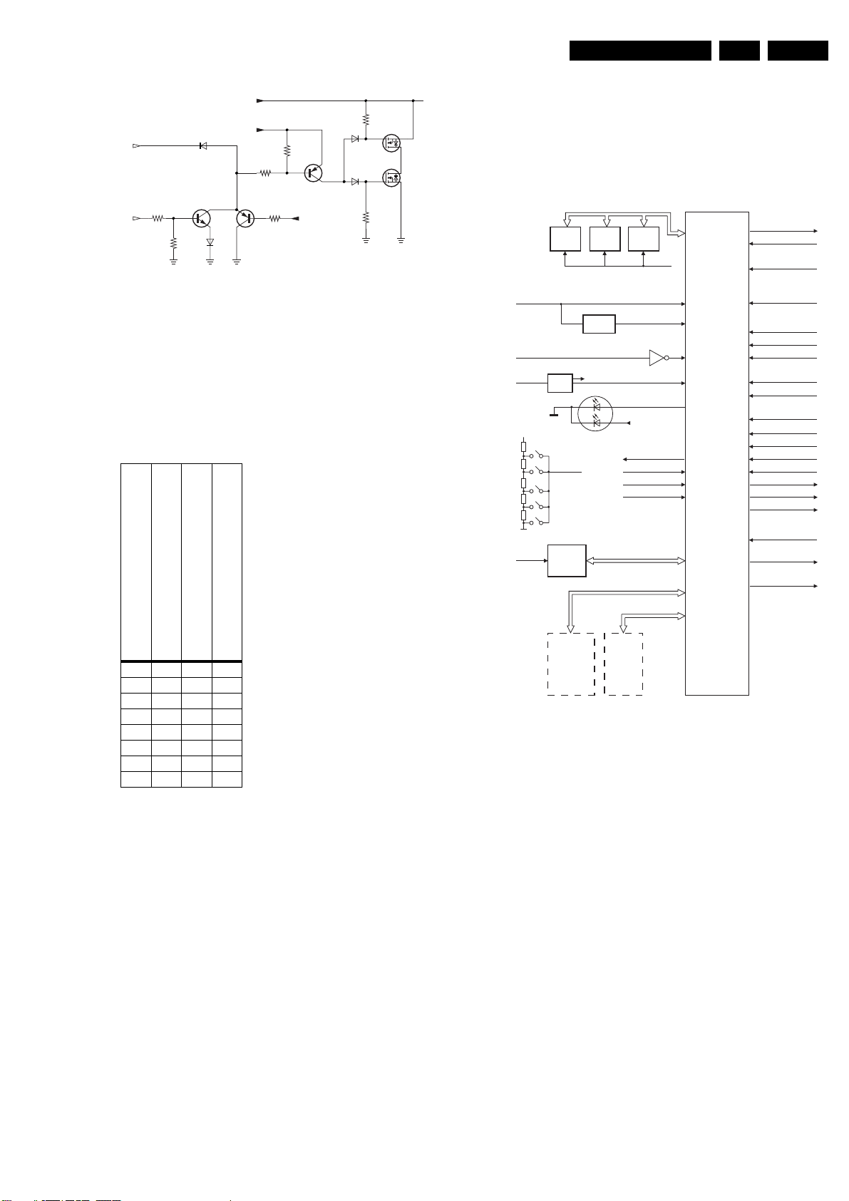
Circuit Descriptions, List of Abbreviations, and IC Data Sheets
EN 93F21RE AB 9.
AUDIO-SIGNAL (LEFT)
+5VSTBY
POWER_VALID
SOUND_ENABLE
3835
10K
6862
7835 7862
68353836150K
3861
3865
47K
10K
3862
10K
7865
+5VSTBY
Figure 9-7 Audio mute circuitry
The table below shows how this is done. It is controlled by the
following signals:
• POWER_VALID line is a control signal generated by the
power supply.
• SOUND_ENABLE line is a control signal coming from the
microprocessor on the SSP.
• +5VSTBY line, from the Front panel.
Table 9-2 Truth table audio mute
3868100K
6868
6867
3867100K
CL16532098_006.eps
7868
7867
180901
9.4.1 SSP: Control
The control part can be divided into:
• Set Control
• TXT/OSD
• Remote Control
Set Control
FLASH
FLASH
(EPG)
(SW)
CVBS-TXT-DW-OUT
PEAKING
FILTER
H, V
+3V3 +
RESET
+3V3
RED
GREEN
UART-OUT
KEYBOARD
+5VSTBY RESET
+3V3
A0...A19 D0...D15
DRAM
(TXT)
STBY-LED
8V6
+5V
+8V6
+3V3
7001
SAA580X
5
7
83,84
74
113
90
107
106
105
120
119
117
114
110
109
108
104
103
100
99
98
97
96
95
94
93
P50-OUT
SAM
SEL_IN_2
IR-LED
LIGHT SENSOR
STATUS SC3
FRONT DETECT
STANDBY
SEL_IN_1
RC5/RC6
POWER-VALID
CONFIG-IDENT
P50-IN
SDM
SOUND ENABLE
RESET AUDIO
ENA-SCALER
POWER_VALID (from PSU)
SOUND_ENABLE (from uP on SSP)
+5VSTBY (from Front Panel)
SIGNAL MUTED
0001
0011
0101
0111
1001
1010
1101
1111
When the SOUND_ENABLE signal is high, the two N-channel
FETs are conducting the audio signal to the GND, and will mute
the audio output.
Why are two FETs implemented? Because in a case of "no
mute", and FET 7868 directly connected to ground, the diode
in this FET would distort the audio signal too much. With the
addition of FET 7867, this distortion is eliminated, because this
FET is connected in anti-series.
The supply for the inverter is connected to the +5VSTBY. This
supply signal is always available when the Mains is connected,
so in case the Mains voltage is disconnected, the mute function
is disabled.
9.4 Small Signal Panel (SSP, diagram K)
The SSP is based on the one used in the MG3.1 chassis. It
consists of the following parts:
1. Control.
2. Video: Tuner and IF.
3. Video: HIP.
4. Video: Feature Box.
5. Video: HOP.
6. Audio
UART-IN
FRAME
RGB, BLENDING
CL 36532021_005.eps
+3V3
EEPROM
M24C32
NVM
TUNER
FDS
3D COMB
I/O SELECT V
I/O SELECT A
AVI
HIP
HOP
FBX
MSP
slow
fast
I2C3
I2C1
I2C2
91/92
85/86
87/88
89
81
77,78,79,80
Figure 9-8 Block diagram Control part (µP)
The SAA5801 (IC7003) is called the OTC (OSD, TXT, and
Control). In this IC, the microprocessor and the TXT-decoder
(or Closed Caption for the USA) are integrated. The SAA5801
is also called the OTC2.5 because also TXT-level 2.5 is
supported.
At start up, the RESET signal is generated with TS7006/7007.
During a reset, all I/O pins are high. When a RESET is
generated, the set is in Standby mode.
The 8V6 and the 5V2 are sensed by pins 105 and 106. If one
of them is not present, the Power supply is switched "off". The
OTC will generate an error code to indicate what was wrong.
The horizontal (HOSD-PIP) and vertical (VD) pulses are also
fed to the OTC for stable OSD and CC. To create good stable
pulses, these signals are inverted and fed to the OTC. The
RGB-outputs (77/78/79) together with fading (pin 80) are fed to
the HOP. This fading pin has a double function:
• Make the menu transparent.
• Fast-blanking for CC.
There are three I2C busses used (see section "I2C overview"):
1. Slow I2C bus (max. 100 kHz) for tuner, DW, video-, and
audio selection.
2. Fast I2C bus (max. 400 kHz) for the HIP, MSP, TOPIC,
HOP, and FBX (PICNIC, and FALCONIC).
3. NVM I2C bus for the Non Volatile Memory to avoid data
corruption.
Page 94
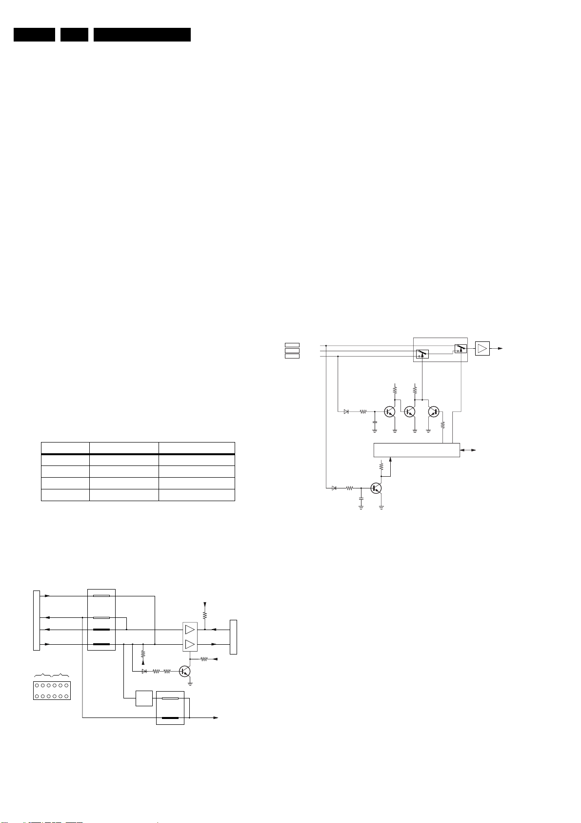
EN 94 F21RE AB9.
Circuit Descriptions, List of Abbreviations, and IC Data Sheets
The OTC also has a connection with the Front panel:
• Driving the "on" and "STANDBY" LEDs.
Service tip: The green LED gives a quick indication that
the 8V6 voltage is present.
• This chassis has an IR send-LED connected to pin 90 for
communication with DST or ComPair.
• The remote control signal comes in on pin 100.
Memory
The set software is in a 4 MB ROM (IC7002) and in a 32 KB
ROM inside the OTC. The level at pin 73 of the OTC
determines whether this internal software is used at start up.
This level is determined with R3026/3029. The external ROM
is driven via the OE and CS signals.
The Non Volatile Memory (NVM) IC7008 is a 32 KB version
M24C32W6, and is used to store
• Software identification.
• Operational hours.
• Error codes.
• Option codes.
•Presets.
• Alignments.
All ICs in this part are supplied with 3V3. For this, a 3V3
stabilizer is used (IC7009).
Monitor communication (UART/FSP)
In total, four versions of the Receiver box are realised. There is
an US and EU version (main difference is the HD part for US).
Furthermore, there will be version for the current 42" FTV1.9
monitor and a version for the new FM2x monitor range. The
difference between these versions is mainly the
communication between the Receiver box and monitor. See
table below:
Table 9-3 Overview UART diversity
Conn. 0303 F21R with FTV1.9 F21R with FM2x
Pin 4 Not used RXDO
Pin 11 CONFIG_IDENT TXDO
Pin 12 TXDO Not used
Pin 15 RXDO Not used
The Receiver box has to support both the FTV1.9 and the
FM2x plasma monitors. The communication protocol for the
FTV1.9 monitor is based on UART with a CONFIG_IDENT
signal. However, all FM2x monitors have a new improved
protocol called FSP (FTV System Protocol). Therefore, the pin
layout on the FTV monitor output connector has been changed.
1519
10
9
FTV2.3
12
11
FTV2.3
2
1
FTV1.9
4
3
FTV1.9
11
1519
7545
one
shot
3595
+5VSTB
7460
FTV2.3
FTV1.9
7
5
7571
CONFIG_IDENT
357635706571
8
6
TO/FROM
MONITOR
0303
4
11
12
15
FTV2.3FTV1.9
13579
24681012
+5VSTB
3596
3577
0355
TXDO
TO µP
(SSP)
RXDO
+5VSTB
CL16532098_008.eps
180901
As the FM2x has no CONFIG_IDENT signal to "wake up" the
Receiver box, a "dummy" CONFIG_IDENT is derived from the
RXDO signal with the aid of a "one-shot generator" (item 7545).
In order to prevent the RXD-line from connecting to ground, a
protection circuit is added. This circuit puts the RXD-buffer into
tri-state if the input is connected to ground for more than 100
ms.
Because the diversity is realized with jumpers (connector
1519), there are no differences in panel stuffing for both
versions.
Teletext/On Screen Display (TXT/OSD)
The TXT/OSD-decoder in the OTC gets its video signal directly
on pin 5. The RGB-outputs are available on pins 77/78/79. Fast
blanking is realized by pin 80. The RAM (IC7001) of the
microprocessor is also used for the decoder.
Remote Control
The remote control uses RC6, because commands like "cursor
control in eight directions" are used.
For this chassis, there are three possible RC input sources:
• RC_MON (coming from monitor),
• RC_BOX (coming from box), and
• RC_EXT (coming from an external source; this is not
used).
The selection is performed as shown in the figure below:
0313-C
0308-6
0303-9
RC_EXT
RC_FRONT
RC_MON
RC_EXT_PRESENT
7749
7880
7881
7740
2
0
5
3
1
7751
I/O expander
RC_EXT_PRESENT_N
RC_FRONT_SEL_N
0
15 RC_OUT
1
7884
RC_FRONT_MON_SEL
RC_FRONT_SEL
Figure 9-10 Block Diagram RC Selection Circuitry
When CONFIG_IDENT (for FTV1.9) or AYT (for FM2x) is
detected, the RC_MON is selected.
If there is no monitor connected, the RC_FRONT_SELECT
signal is always "low", so RC _MON cannot be selected (via
TS7749 and TS7751). After start up, when the I/O-expander is
not yet set via I2C, the RC_FRONT signal is connected to
RC_OUT.
I2C
CL16532098_007.eps
to SSP
180901
Figure 9-9 Block Diagram UART Circuitry
Page 95
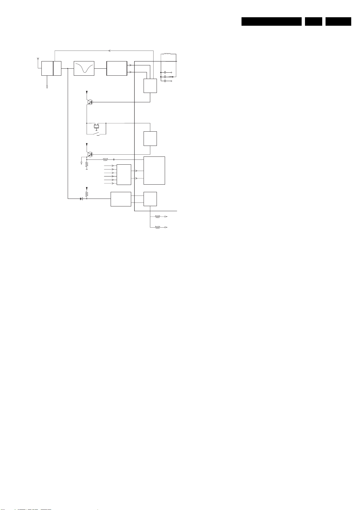
Circuit Descriptions, List of Abbreviations, and IC Data Sheets
EN 95F21RE AB 9.
9.4.2 SSP: Tuner and IF
1
1102
11
TUNERSPLITTER
TO DW TUNER
40,4
+8V6
+
CVBS-TER
+5V
6102
The demodulated video signal is available at pin 10, and then
fed to a sound-trap. This is for filtering the rest sound carrier.
AGC TUNER
1109 75015103
FILTER VIDEO
L5108
SAW
3
2
62 758
Then the group delay time (system dependent) can be
adapted, and at pin 13 of the HIP, the CBVS is available for
further processing in the set.
The tuner-IF signal is also fed to a second SAW filter for the
sound. At pin 5 of the HIP, the IF-sound is available. This signal
VIF
DEMOD
7111
1106
5.5MHz
10
HIP
TDA9320H
12
is fed to the MSP for further processing (the IF-sound is
demodulated by the MSP3410).
9.4.3 SSP: HIP (High-end Input Processor, diagram K1)
Introduction
The HIP (IC7501, TDA9320H) has the next functions:
• Source selection.
BG/BG
7502
3560
PLUG
EXT1
EXT2
SOURCE
EXT3
SELECT
EXT4
FRONT
3109
1104
FILTER SOUND
SAW
DELAY
OPTIM BG
OR
FLAT
13
14
VIDEO
SWITCH
63
SIF
64
• Video IF-demodulation.
• Luminance, chrominance, and sync processing.
Inputs
The set has a total of five external inputs (AV1 - 5).
The HIP has an integrated source selector, which can handle:
• 3 CVBS inputs.
• 2 Y/C inputs.
• 2 RGB inputs.
The HIP detects whether the input is Y/C or CVBS and decides
what to do. There are two inputs (pins 39 and 40) for detection
of the RGB status. The other status voltages are checked by
AM SOUND
the OTC.
SIF MSP
CL 06532023_046.eps
240901
Figure 9-11 Overview Tuner and IF Part
Normally for chassis with the Double Window feature, a splitter
is used. This splitter is on the chassis, beside the main tuner.
From this splitter, the aerial signal is fed to the main tuner on
the SSP and the DW tuner on the DW panel (which is not
present in this chassis). Therefore, the aerial input is on the
splitter.
The tuner part contains a tuner and an oscillator-mixer. The
tuner is I2C controlled. The reference voltage at pin 9 is 33 V.
This voltage (V_TUN) is derived from the secondary side of the
standby supply. The OTC, together with the HIP, controls the
tuning procedure.
The frequency of the local oscillator is compared with the
frequency of a reference oscillator by a PLL. The varicap
voltage is changed via I2C, and that changes the frequency of
the reference oscillator.
For the higher frequencies, the tuning speed is increased by
increasing the current that changes the varicap voltage.
The IF-part can be split into two important parts:
1. The IF-filter.
2. The IF-amplifier and demodulator.
The IF signal is fed to a SAW filter (item 1109 for the video and
1104 for the audio). The output of this filter is fed to the HIP for
demodulation. The demodulator is PLL-controlled via a VCO.
This VCO is I2C controlled (Service Alignment Mode IF-AFC
alignment). Tuning of the VCO is possible by switching some
small capacitors parallel to L5108. These capacitors are
integrated in the HIP.
In addition, the AGC takeover point is I2C controlled (with the
SAM menu).
Service tip: If the AFC is not adjusted correctly, very strange
faults can occur: like spontaneous standby switching, cracking
sound, incorrect CC, etc.
Video Processing
• The video identification block monitors whether a video
signal is detected at one of the inputs. The Y/C switch
detects whether the input is CVBS or Y/C, and switches
these signals for luminance and chrominance processing.
If a comb filter is used, the HIP detects they are "combed",
and the YC switch will select the signals for the comb filter.
The comb filter can be switched to the right system via the
two system lines (SYS1 and SYS2) from the HIP.
• If the input signal is CVBS, then an internal colour trap is
used in the Y path.
• The Y-delay can be controlled via the service menu to
match the colour to the luminance (because of different
signal paths there are different timings)
• Via the RGB-matrix, external RGB-signals are converted to
YUV, for further 2fH conversion.
• The internal YUV switch switches between the
demodulated video signal and an external RGB source.
• The sync processor in the HIP provides H_A and V_A sync
signals for the Feature Box. This sync part is alignment
free, but it should be noted that the line oscillator is locked
with the colour oscillator.
Note: If the quartz crystal is defective, there will be no colour
and synchronization problems. This crystal is very precise: if it
is replaced by another type, there may be no colour, because
of a different capacity. Therefore, you must use the genuine
replacement part.
Outputs
The HIP has the following outputs:
• YUV (50 Hz), for further picture processing on pins 49, 50
and 51.
• CVBS-DW, video signal for the Double Window module (if
present) on pin 32.
• CVBS-SC2-OUT, monitor output (WYSIWYR = What You
See Is What You Record).
• CVBS-TXT-OUT, CVBS for TXT and Comb filter.
• CVBS-TER, video signal from the tuner is fed to the I/O
switching and to EXT1 on pin 19 of SCART.
Page 96
EN 96 F21RE AB9.
Circuit Descriptions, List of Abbreviations, and IC Data Sheets
9.4.4 SSP: Feature Box (FBX, diagram L)
Introduction
The basic function of the Feature Box (FBX) is picture
improvement, and depending on the version, several scan
IC 7714
MS81V04160
MEM1
8UV
8Y
WE IE
BUS C
FILTERS
HA
VA
ADC
8UV
conversion methods are possible. The PICNIC (SAA4978H) is
the central key component.
Block diagram
IC 7718
SAA4992
8Y
8UV
8Y
RE D
BUS D
FALCONIC
8UV
8Y
IC 7713
SAA4978H
DAC
IC 7717
MEM 2
IC 7719
(OPTIONAL)
MEM 3
YUV_FEAT
100Hz
DIG
SCAN
FILTERS
TO TOPIC
PICNIC
ACTIVE
'HIGH'
.139
HD
VD
A0...A7
ALE
ACTIVE
'HIGH'
EN
A8...A15
A0...A7
IC 7711
M27C512
64k PROM
Figure 9-12 Block Diagram FBX7
The 50 Hz YUV signals, coming from the HIP, are fed to the
PICNIC via an anti-aliasing filter.
The (AABB) "frame frequency doubling" is done by the PICNIC
(SAA4978, 160 pins QFP) together with a field memory
(MEM1). The PICNIC can handle most 100 Hz functions
(except Progressive Scan).
Via bus "C", a digitalized signal is presented to MEM1 (Field
Memory 1), which is used for the 50 to 100 Hz conversions. The
signal goes further via the data-bus to the FALCONIC. This IC
has the following functions:
• Line flicker reduction.
• Digital Noise Reduction (DNR).
• Progressive scan.
It has an internal CPU and a (small) integrated ROM. The
actual FBX7 software is located in an external ROM (item
7711). In order to limit the number of connections between the
PICNIC and the external ROM, a number of lines are used
twice. The lines A8 to A15 are fixed lines, while the lines A0 to
A7 are made switchable with the eight data lines of the ROM.
This is done via a Latch (item 7712), which is controlled by pin
139 of the PICNIC (the ALE signal).
At the end, the digital YUV (YUV_FEAT) signals from the
PICNIC (pins 12, 14, and 15) enter the TOPIC.
This IC has the following functions:
• Luminance Transient Improvement (LTI).
• Peaking.
• Colour transients (CTI) and colour enhancement (TOPIC).
IC 7712
LATCH
IC
D0...D7
CL 36532021_018.eps
The digital YUV-signals from the PICNIC go, via a passive
output filter, to the TOPIC and then to the HOP.
PICNIC (Diagram L1)
The PICNIC has the following functions:
• ADC/DAC.
• Interlaced to progressive scan conversion.
• Dual screen compression
• The Panorama mode.
• Automatic Aspect Ratio Adaptation (AARA)
• Colour Transient Improvement (CTI)
• The contrast improvement (Dynamic Contrast).
All these functions are integrated in one IC: the SAA4978H,
160 pins QFP.
ADC/DAC
• Analogue to Digital conversion is done with three identical
9-bit ADCs.
• Digital to Analogue conversion uses three identical 10-bit
DACs.
In the PICNIC, there are three nine-bit ADCs present for Y, U,
and V. For digitising the Y (luminance), nine bits are used (to
realize a more detailed picture). These nine bits are only
internally used. Via dithering, the nine bits are reduced to eight
bits and this data is stored into memory. The data in the
memory is fed back to the PICNIC and via un-dithering the data
is again reproduced to nine bits for processing.
280303
Page 97
Circuit Descriptions, List of Abbreviations, and IC Data Sheets
EN 97F21RE AB 9.
U/V (colour difference signals) is also sampled with nine bits.
These two nine bit data streams are multiplexed to four bit data
streams. As the perception of colours by the human eye is less
sensitive to luminance, this reduction is allowed.
Interlaced to progressive scan conversion
The main function of the PICNIC is the "Analogue to Digital"
conversion, spatial noise reduction, histogram functions (like
Dynamic Contrast and Black Stretch) for YUV, and HV-sync
processing. Also, the line frequency is doubled.
De-interlacing itself is realized in the FALCONIC (Field And
Line CONverter IC).
Further features of the PICNIC:
• Dual Screen Compression. The PICNIC can provide
horizontal video compression up to 50 %. The compress
mode can be used to display dual screens.
• The Panorama Mode. To fit 4:3 pictures into a 16:9
display, it is possible to apply a panoramic horizontal
distortion, to make a screen-fitting picture without black
sidebars or lost video. The centre horizontal gain is
programmable and the side gain is automatically adapted
to make a screen-fit.
• Automatic Aspect Ratio Adaptation (AARA). This
feature uses data from the "black bar detection circuit" to
adapt the vertical and horizontal amplitude to an aspect
ratio belonging to the display, without the black bars.
• Dynamic Contrast. To make the contrast (black/white)
range wider, Philips has invented Dynamic Contrast. It
uses the digital memory used in 100 Hz sets. It measures
every A-field (25 x per second), and digitally analyses
where on the greyscale most of the image is located. If it is
a relatively dark image, the lighter part of that image is
stretched towards white, so that more contrast will become
visible in that picture. If it is a relatively light image, the
darker part of that image is stretched towards black, so that
these darker parts will have more contrast. When the
image is in the middle of the greyscale, both dark and light
parts are stretched.
FALCONIC (Diagram L3)
Besides "Natural Motion", The FALCONIC (Field And Line
CONverter IC) has the following functions:
• Line flicker reduction (Digital Scan).
• Noise reduction (DNR, Dynamic Noise Reduction).
• Vertical Zoom.
• Movie phase detection.
• Progressive scan.
• Variable vertical sample rate conversion.
• Synchronous No parity Eight bit Reception and
Transmission interface (SNERT).
422 processing
The FALCONIC can do "422" processing. This means eight
data lines for Y and eight data lines for U/V (844 = 422).
Therefore, the bandwidth for the colour difference increases:
the bandwidth for Y remains 6 MHz, and the bandwidth for
colour difference is now 3 MHz. This means that the picture for
DVD is much better. For this extra bandwidth, an extra field
memory is used: IC7640.
MFO1 MF016
CL 16
CL 16
7634 7602
3V3
CL 32
SR
RE RE
10
SW
CK
CK
13
MEM1A
OE OE
UV
C1 C4
R
R
S
S
T
T
W
R
(100Hz)(50Hz)
BUS C
SW
CK
MEM1B
I
W
E
E
I
I
C
C
SR
CK
Y
C1 C8
UV
C5 C8
PICNIC
CL 32
IEE
YD0 YD7
UV D0 UV0
FE04 FF11
FE00 FE03
YB0 YB7
UVB0 UVB3
YC0 YC7
UVC0 UVC3
RE
IC7638
CL 32 CL 32
IC7640
CL 32 CL 32
3V3
BUS A
FALCONIC
BUS F
Y01
D8
UVD1
D8
BUS D
WE_D
BUS D
BUS E
WE_B
BUS B
BUS C
Figure 9-13 Block Diagram Digital Scan
Bus A is the input bus for the FALCONIC. The data comes from
the two memory ICs (IC7602 and 7634) and the FALCONIC will
cluster this data. It is possible to connect two field memories to
the FALCONIC. The output of the FALCONIC is fed back to the
PICNIC via bus D.
The FALCONIC has two possible configurations:
• Economy mode: In this mode, only Field Memory 2 is
mounted (saving the cost of Field Memory 3). In this
configuration, the full frame store can be made by a factor
2 data compression, using 2 dimensional DPCM
techniques. This results in a performance with more
quantisation noise, while maintaining improved MEMC
quality. In this case, a full "422" processing cannot be
achieved. Only the 422-DPCM is possible.
• Full functionality mode: This configuration uses Field
Memory 2 and 3. Therefore, no picture performance
concessions are made here. In this mode, all FALCONIC
features can be applied optimally. However, to be able to
perform full "422" processing, the FM1 must be extended
with an extra 4 bits, for a total of 16 bits.
Power Supply and RESET Circuit
Besides the two incoming voltages, 8V6 and 5V2, two
stabilizers (for power consumption reasons) are used for the
3V3 (3V3A and 3V3B).
3603
3610
8V6
3V3B
+3V3F
3V3P
3V3A
3680
3608
PICNIC
20mS
6 µP RESET
7 WD RESET (WATCH DOG)
2mS
8V6
5640
5V
5V
7631
5606
7630
+5V
3683
7600
3601
3605
3609
3604
C2690
C2656
7601
+5V
WE IE OE
MEM2
+5V +5V
WE IE OE
MEM3
+5V
RSTRRSTR
CL 16532023_049.eps
210901
Improved motion detection (Natural Motion)
This set utilizes AB'A'B scanning, a new sample for Natural
Motion.
The FALCONIC has an extra advantage for motion detection:
the maximum number of pixels that can be followed in AB’A’B
scanning is higher: This produces a more natural motion, even
with very fast movements.
Improved line flicker reduction (Digital Scan)
The FALCONIC offers motion compensated line flicker
reduction. This virtually leads to complete elimination of line
flicker.
7613
7612
+5V
+3,3VB
DETECTION 3V3
CL 16532023_050.eps
240901
Figure 9-14 Block Diagram Reset Circuitry
Via the reset circuit (TS7600/TS7601) a pulse of 20 ms is
generated for the µP (in the PICNIC) and for the ROM. After
power "on", the 3V3 is built up, which is derived from the 5V2.
As long as the 5V2 is below the 3V3, the 3V3 follows the 5V2.
Page 98
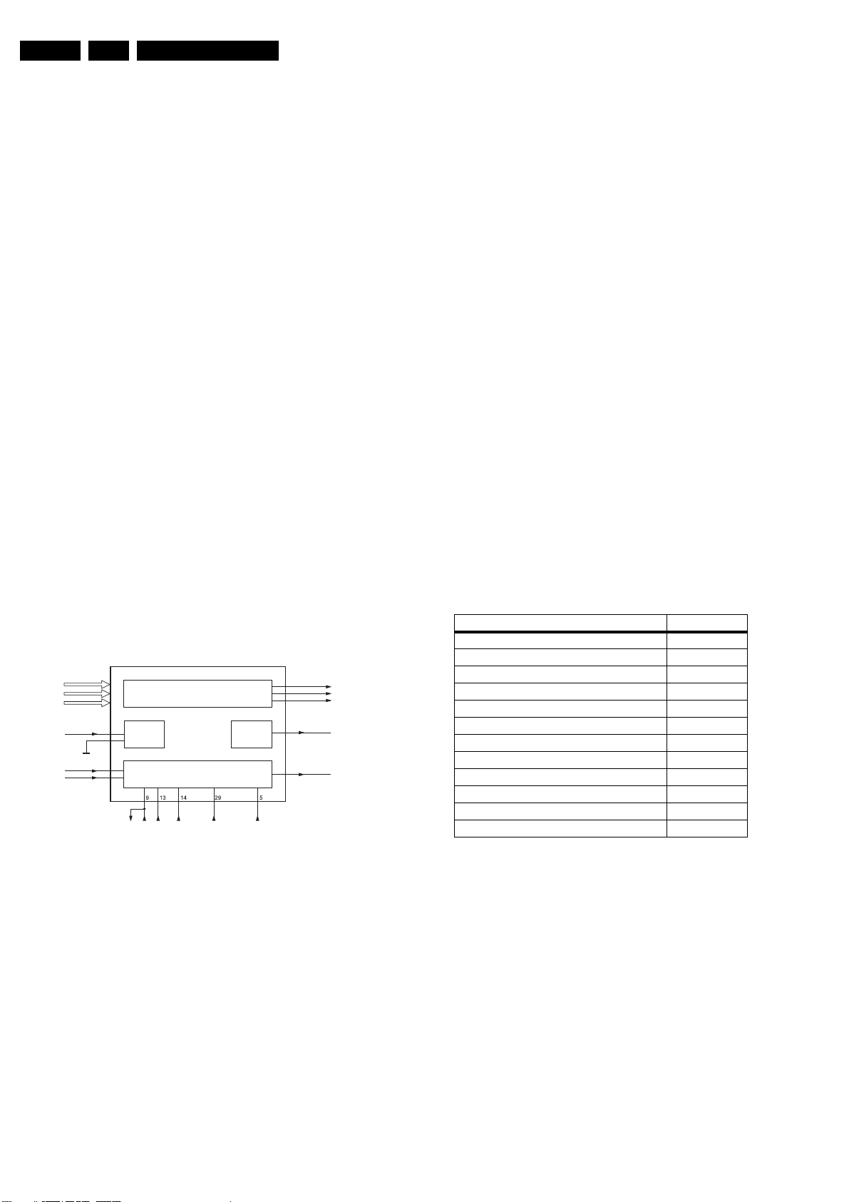
EN 98 F21RE AB9.
Circuit Descriptions, List of Abbreviations, and IC Data Sheets
TS7600 blocks and so does TS7601. The voltage on pin 6 of
IC7611 increases in the same way as the 3V3.
If the 5V2 rises above 3V3, the 3V3 stabilizes and TS7600
starts to conduct. Capacitors C2656//C2690 are charged by
R3604 and R3605. At a voltage of 0.6 V, TS7601 will conduct
and the voltage at pin 6 of IC7611 becomes low again. The (P
is reset now.
If the PICNIC cannot communicate with the ROM, a reset is
generated by the watchdog. Pin 7 of the PICNIC generates a
pulse to create a new reset pulse for pin 6.
If one of the two supply voltages (3V3A, 3V3B) is absent, a
safety problem could occur. The 3V3A is the supply voltage for
the PICNIC and the 3V3B for the FALCONIC. If the 3V3 is too
low, the base of TS7601 will be low via TS7612 and TS7613. If
the base of TS7601 is made low, a RESET signal is generated
for the PICNIC.
9.4.5 SSP: TOPIC and HOP (Diagram K6)
Introduction
The TOPIC (The most Outstanding Picture improvement IC,
item 7402, type TDA9178), is an (optional) IC between the
PICNIC and the HOP. It has the following (picture
improvement) functions:
• Luminance Transient Processor (LTP), for detail
enhancement.
• Chrominance delay circuitry, to compensate timing
differences between Y and C.
• Spectral processor , for improved sharpness and colour
transient improvement (CTI).
• Colour vector processor, for skin tone correction, green
enhancement and blue stretch.
• Measure and detection circuitry, for AutoTV.
The sandcastle pulse from the HOP (High end Output
Processor), is fed to pin 1 of the TOPIC, which is used as
reference for timing.
IC 7300 / TDA9330H
Y, U, V FEAT
RGB PIP
RGB TXT
8V6
HD
VD
SC
1FH/2FH
VIDEO CONTROL
VFB HFB DYN
TDA 9330 AH
H O P
GEOMETRY
PHASE
CORR.
FBCSO
SUPPLY DAC
R
G
B
HOP DAC
LINE DRIVE
CL 16532023_053.eps
240901
9.4.6 SSP: Audio processing
Introduction
The sound processing is distributed between the Flat Monitor
(amplifier) and the Receiver Box (processing). The sound
processing in the Receiver Box is completely done by the:
MSP 3410D: demodulation for Europe and AP (including
NICAM), or
MSP 3440G: demodulation for US/LatAm/Taiwan (this IC also
covers Korean stereo).
The MSP ICs contain audio processing, used for the basic L/R
stereo sound. This processing involves bass, treble (via the
equalizer), and balance (trim speakers). The volume is set to a
fixed value, because the volume control is done in the monitor
(via UART).
With the user interface, audio selection can be "mono",
"stereo", or "surround" mode (surround mode will give spatial
functionality). Stereo and spatial is only possible if a stereo
signal is available.
All the extra audio sources, compared with the SSP, can be
used in the main channel. The "Centre" input is available on the
AV-interface panel. With this input, it is possible to use the
monitor left and right speakers as a centre speaker in a home
cinema configuration. This input can be selected via the User
Interface.
For VGA it is not possible to select the "Centre" input, because
the E-box OSD is not working for VGA inputs.
The selection of the possible inputs is divided over two
separate panels: the SSP and the AVI panel. The input
configuration dependents on the E-box version (in combination
with a TEA6422 (item 7777), the MSP is also used for a part of
the source selection in the E-box).
Table 9-4 Audio I/O overview
Audio inputs and outputs (EU/AP) Location
RF input SSP
EXT1= SCART1 L/R-in and L/R-out SSP
EXT2= SCART2 L/R-in and L/R-out SSP
EXT3= SCART3 L/R-in SSP
EXT4= SCART4 L/R-in SSP
SD L/R (YPbPr-1fH) SD panel
VGA L/R-in AVI panel
Center audio in AVI panel
Front L/R-in Front panel
VGA audio out for FTV monitor L/R-out AVI panel
CL-out for a Dolby audio receiver SSP
Headphone out L/R Front panel
Figure 9-15 Block diagram HOP
The video processor and digital deflection processor are
integrated in the HOP (IC7300, TDA9330H). Its main functions
are:
• RGB interface for OSD/CC.
• Control of saturation, contrast, and brightness.
• Black/blue stretch.
Operation
After input selection, the YUV input is converted to RGB
outputs. The RGB and fast blanking from the OTC (OSD and
CC) are inserted on pins 35 - 38.
Blue stretch, measures the amplitude of the three RGB signals.
If one of these colour signals reaches more than 80% of the
nominal value, the amplification of Red and Green decreases.
This is to achieve a higher colour temperature.
The RGB outputs are available at pins 40 - 42. They are
buffered and fed to connector 0340, which goes to the AVinterface.
9.5 Front Panel (FP, diagram FP)
9.5.1 General
This panel serves as an interface with the "outside world", and
has the following inputs/controls/indicators:
• Power switch.
• Power LED.
• Audio L/R in.
• Video CVBS in.
• Video SVHS in.
• Headphone out.
• IR send-LED and receiver-LED (for Service).
• IR receiver (for Remote Control).
• Control buttons for MENU, PROGRAM, and VOLUME.
Page 99
Circuit Descriptions, List of Abbreviations, and IC Data Sheets
EN 99F21RE AB 9.
9.5.2 Audio path
Front audio inputs (SNDL/R_FRONT) are connected to the
TEA6422 (item 7810) on the AV-Interface.
The headphone output signal (DS_AUDIO_L/R) from the DW
module is routed to the front panel.
9.6 Auto TV
The Auto Picture Control (or AutoTV) aims at giving the
customer the best possible picture performance at any time.
Therefore, it does a real time processing of the video signal
and, as a result, it decides to adapt several video parameters
throughout the whole chassis. The user can choose the total
effect of the Auto Picture Control on the screen via the remote
control.
AutoTV consists of a set of algorithms that perform the
following tasks:
• Auto Noise Reduction:
– Input: noise measurement done in PICNIC.
– Output: noise reduction of PICNIC, coring of PICNIC,
TOPIC (if present), or EAGLE (if present).
• Auto Sharpness:
– Input: steepness information and band energy in
PICNIC.
– Output: sharpness settings in PICNIC, TOPIC (if
present), or EAGLE module (if present).
• Auto Ambient Light (in combination with histogram):
– Input: light sensor information (from TV monitor).
– Output: is depending on the user setting of Active
Control. If "maximum", saturation and contrast of the
HOP and histogram settings in PICNIC. If "medium",
only HOP saturation and PICNIC histogram.
• Auto colour:
– Input: user smart mode choice.
– Output: colour features of the EAGLE (or TOPIC), like
green enhancement and skin tone correction.
The FTV E-Box has no own light sensor, instead they is
featured in the TV monitors. The E-box is involved in the image
control loop for these light sensors. The 42" F19D and 50”
FM25 monitor do not have a light sensor.
The user can select four different settings: OFF, MIN, MED and
MAX. The setting does not change the amount of the influence
of the algorithms on the screen, but partly switches algorithms
ON (see table below).
Table 9-5 Active Control settings
Active Control OFF MIN MED MAX ON (**)
Auto Ambient off off on (*) on off
Auto Color (***) (***) (***) (***) (***)
Auto Histogram on on on on on
Auto Sharpness on on on on on
Auto Noise off on on on on
(*) In MEDIUM, the monitor contrast coupling of ambient is not
working.
(**) When the light sensor is not present, ambient light control
is not possible and the setting of the AutoTV button is limited to
OFF/ON.
(***) Independent of Active Control is OFF/MIN/MED/MAX.
Dependent of colour enhancement setting (in picture menu)
and smart picture mode.
9.7 Abbreviation list
ADC Analogue to Digital Converter
AM Amplitude Modulation
AP Asia Pacific
ATSC Advance Television Systems
Committee
AV External Audio/Video
AVI Audio and Video Interface
B/G Monochrome TV system. Sound
carrier distance is 5.5 MHz
BTSC Broadcast Television Standard
Committee. Multiplex FM stereo sound
system, originating from the USA and
used in LATAM and AP-NTSC
countries
CBA Circuit Board Assembly (Printed
Circuit Board)
ComPair Computer aided rePair
CSYNC Composite SYNC
CVBS Composite Video Blanking and
Synchronization
DAC Digital to Analogue Converter
D/K Monochrome TV system. Sound
carrier distance is 6.5 MHz
DFU Directions For Use: owner's manual
DNR Dynamic Noise Reduction
DRAM Dynamic RAM
DSP Digital Signal Processing
DTS Digital Theatre Sound
DVD Digital Video Disc
DW Double Window
E-box Electronic box (Receiver box)
EEPROM Electrically Erasable and
Programmable Read Only Memory
EU EUrope
EXT EXTernal (source); entering the set by
SCART or cinch (jack)
FALCONIC Field And Line CONverter IC
FBX Feature BoX
FLASH FLASH memory
FM Field Memory or Frequency
Modulation
FSP FTV System Protocol
FTV Flat TV (plasma screen)
HD High Definition
HFB Horizontal FlyBack
HP HeadPhone
I Monochrome TV system. Sound
carrier distance is 6.0 MHz
I2C Integrated IC bus
I2S Integrated IC Sound bus
IF Intermediate Frequency
Interlaced Scan mode where two fields are used
to form one frame. Each field contains
half the number of the total amount of
lines. The fields are written in "pairs",
causing line flicker.
IR Infra Red
IRQ Interrupt ReQuest
LATAM LATin AMerica
LED Light Emitting Diode
L/L' Monochrome TV system. Sound
carrier distance is 6.5 MHz. L' is Band
I, L is all bands except for Band I
LS LoudSpeaker
M/N Monochrome TV system. Sound
carrier distance is 4.5 MHz
MOSFET Metal Oxide Semiconductor Field
Effect Transistor
MPEG Motion Pictures Experts Group
NC Not Connected
Page 100

EN 100 F21RE AB9.
Circuit Descriptions, List of Abbreviations, and IC Data Sheets
NICAM Near Instantaneous Compounded
Audio Multiplexing. This is a digital
sound system, used mainly in Europe.
NTSC National Television Standard
Committee. Colour system used
mainly in North America and Japan.
Colour carrier NTSC M/N = 3.579545
MHz, NTSC 4.43 = 4.433619 MHz
(this is a VCR norm, it is not
transmitted off-air)
NVM Non-Volatile Memory: IC containing
TV related data (for example, options)
OC Open Circuit
OSD On Screen Display
P50 Project 50 or Easy Link
PAL Phase Alternating Line. Colour system
used mainly in Western Europe
(colour carrier = 4.433619 MHz) and
South America (colour carrier PAL M =
3.575612 MHz and PAL N = 3.582056
MHz)
PCB Printed Circuit Board
PCM Pulse Code Modulation
PICNIC Picture Improvement Combined
Network IC
PIP Picture In Picture
PLL Phase Locked Loop. Used, for
example, in FST tuning systems. The
customer can directly provide the
desired frequency
Progressive Scan Scan mode where all scan lines are
displayed in one frame at the same
time, creating a double vertical
resolution.
RAM Random Access Memory
RC Remote Control transmitter
RC5 Remote Control system 5, the signal
from the remote control receiver
RGB Red, Green, and Blue
RGBHV Red, Green, Blue, Horizontal sync,
and Vertical sync
ROM Read Only Memory
RXD Receive Data (UART)
SCART Syndicat des Constructeurs
d'Appareils Radiorecepteurs et
Televisieurs
SCAVIO Scaler Control Audio Video Input and
Output
SCL Serial CLock I2C
SD Standard Definition
SDA Serial DAta I2C
SDRAM Synchronous DRAM
SECAM SEequence Couleur Avec Memoire.
Colour system used mainly in France
and Eastern Europe. Colour carriers =
4.406250 MHz and 4.250000 MHz
SMPS Switch Mode Power Supply
SND SouND
S/PDIF Sony Philips Digital InterFace
SRAM Static RAM
SSP Small Signal Panel
STBY STandBY
SVHS Super Video Home System
SW SoftWare
THD Total Harmonic Distortion
TOPIC The most Outstanding Picture
improvement IC
TXD Transmit Data (UART)
TXT TeleteXT
UART Universal Asynchronous Receiver
Transmitter
uP Microprocessor
VCR Video Cassette Recorder
VGA Video Graphics Array
YPbPr Component video (Y= Luminance, Pb/
Pr= Colour difference signals)
Y/C Luminance (Y) and Chrominance (C)
signal
YUV Component video
0/6/12 SCART switch control signal on A/V
board. 0 = loop through (AUX to TV), 6
= play 16:9 format, 12 = play 4:3
format
480i 480 visible lines, interlaced
480p 480 visible lines, progressive scan
1080i 1080 visible lines, interlaced
1080p 1080 visible lines, progressive scan
 Loading...