

Philips ED1502 Datasheet
DISCRETE SEMICONDUCTORS
DATA SH EET
ook, halfpage
M3D186
ED1502
NPN general purpose transistor
Product specification
Supersedes data of 1997 May 01
1999 Apr 27
Philips Semiconductors Product specification
NPN general purpose transistor ED1502
FEATURES
• Low current (max. 25 mA)
• Low voltage (max. 20 V)
• High gain.
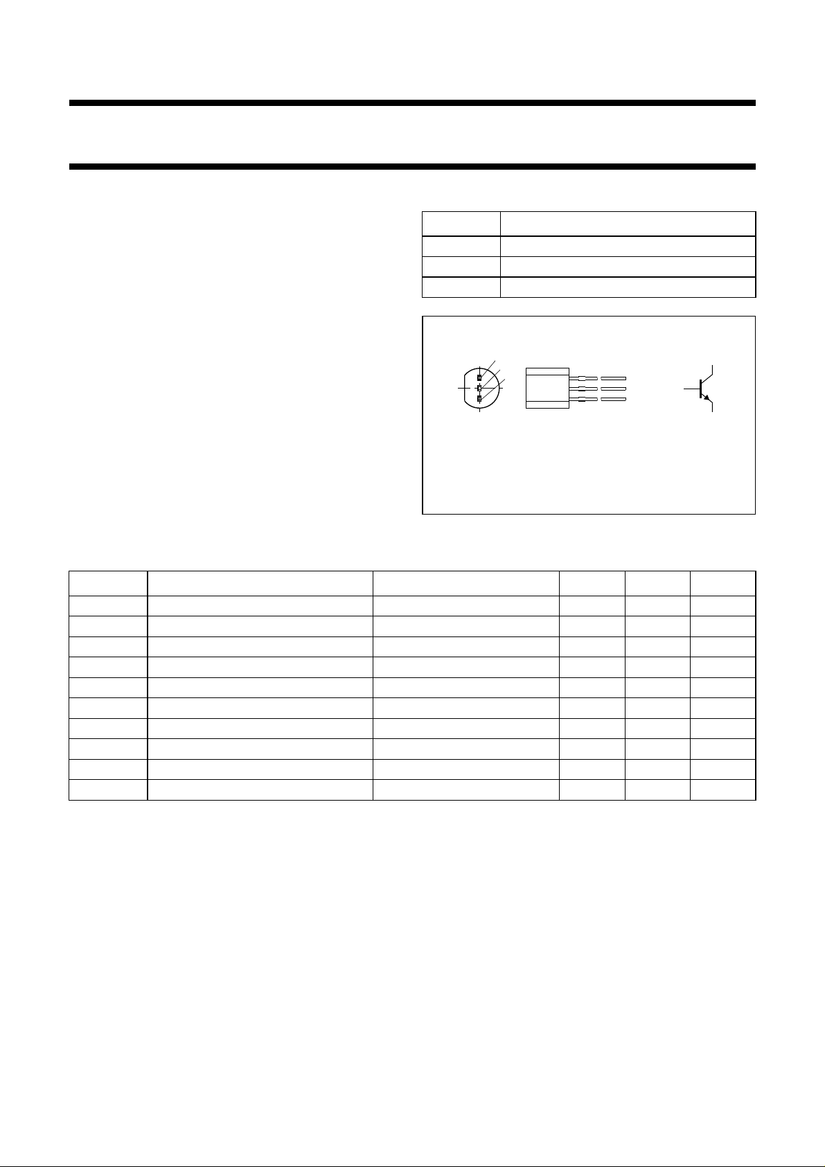
PINNING
PIN DESCRIPTION
1 emitter
2 base
3 collector
APPLICATIONS
• General purpose switching and amplification.
handbook, halfpage
DESCRIPTION
NPN transistor in a plastic TO-92; SOT54 package.
1
2
3
2
MAM182
Fig.1 Simplified outline (TO-92; SOT54)
and symbol.
LIMITING VALUES
In accordance with the Absolute Maximum Rating System (IEC 134).
SYMBOL PARAMETER CONDITIONS MIN. MAX. UNIT
V
CBO
V
CEO
V
EBO
I
C
I
CM
I
BM
P
tot
T
stg
T
j
T
amb
collector-base voltage open emitter − 40 V
collector-emitter voltage open base − 20 V
emitter-base voltage open collector − 4V
collector current (DC) − 25 mA
peak collector current − 25 mA
peak base current − 25 mA
total power dissipation T
≤ 25 °C; note 1 − 500 mW
amb
storage temperature −65 +150 °C
junction temperature − 150 °C
operating ambient temperature −65 +150 °C
3
1
Note
1. Refer to TO-92; SOT54 standard mounting conditions.
1999 Apr 27 2
Philips Semiconductors Product specification
NPN general purpose transistor ED1502
THERMAL CHARACTERISTICS
SYMBOL PARAMETER CONDITIONS VALUE UNIT
R
th j-a
Note
1. Refer to TO-92; SOT54 standard mounting conditions.
CHARACTERISTICS
=25°C unless otherwise specified.
T
amb
SYMBOL PARAMETER CONDITIONS MIN. TYP. MAX. UNIT
I
CBO
I
EBO
h
FE
V
BE
C
re
f
T
thermal resistance from junction to ambient note 1 250 K/W
collector cut-off current IE= 0; VCB=40V −−10 µA
I
= 0; VCB= 20 V; Tj= 150 °C −−5µA
E
emitter cut-off current IC= 0; VEB=4V −−10 µA
DC current gain IC= 7 mA; VCE=10V
ED1502B 48 − 75
ED1502C 66 − 100
ED1502D 84 − 127
ED1502E 105 − 210
base-emitter voltage IC= 7 mA; VCE= 10 V; note 1 −−925 mV
feedback capacitance IC=ic= 0; VCB= 10 V; f = 1 MHz − 0.5 − pF
transition frequency IC= 10 mA; VCE= 5 V; f = 100 MHz 361 − 825 MHz
Note
1. Pulse test: t
≤ 300 µs; δ≤0.02.
p
1999 Apr 27 3
 Loading...