

Philips DVP-620-VR Service manual

DVD + VCR Combi
DVP620VR
/04
Service
Service
Service
Service Manual
Contents
Chapter
Technical Specifications
Sec. 1:
Schematic Diagrams and CBA's
Exploded Views
Mechanical and Electrical Parts Lists
Sec. 2:
Standard Maintenance
Mechanism Alignment Procedures
Disassembly / Assembly of Mechanism
Deck Exploded Views
c Copyright 2004 Philips Consumer Electronics B.V. Eindhoven, The Netherlands
All rights reserved. No part of this publication may be reproduced, stored in a retrieval
system or transmitted, in any form or by any means, electronic, mechanical, photocopying,
or otherwise without the prior permission of Philips.
Survey of versions:
/04 PAL
CLASS 1 LASER PRODUCT
KLASSE 1 LASER PRODUKT
KLASS 1 LASER APPARAT
CLASSE 1 PRODUIT LASER
Published by FU 0436 Service AVS Printed in The Netherlands Subject to modification
Version 1.0
GB 3139 785 30810

MAIN SECTION
DIGITAL VIDEO DISC PLAYER &
VIDEO CASSETTE RECORDER
Sec. 1: Main Section
I Adjustment Procedures
I Schematic Diagrams and CBA’s
I Exploded Views
I Mechanical and Electrical Parts List
TABLE OF CONTENTS
LASER BEAM SAFETY PRECAUTIONS . . . . . . . . . . . . . . . . . . . . . . . . . . . . . . . . . . . . . . . . . . . . . . . . . . . . . 1-1-1
IMPORTANT SAFETY PRECAUTIONS . . . . . . . . . . . . . . . . . . . . . . . . . . . . . . . . . . . . . . . . . . . . . . . . . . . . . . 1-2-1
STANDARD NOTES FOR SERVICING . . . . . . . . . . . . . . . . . . . . . . . . . . . . . . . . . . . . . . . . . . . . . . . . . . . . . . 1-3-1
FUNCTION INDICATOR SYMBOLS . . . . . . . . . . . . . . . . . . . . . . . . . . . . . . . . . . . . . . . . . . . . . . . . . . . . . . . . . 1-4-1
PREPARATION FOR SERVICING . . . . . . . . . . . . . . . . . . . . . . . . . . . . . . . . . . . . . . . . . . . . . . . . . . . . . . . . . . 1-5-1
OPERATING CONTROLS AND FUNCTIONS . . . . . . . . . . . . . . . . . . . . . . . . . . . . . . . . . . . . . . . . . . . . . . . . . 1-6-1
SIGNAL NAME ABBREVIATIONS . . . . . . . . . . . . . . . . . . . . . . . . . . . . . . . . . . . . . . . . . . . . . . . . . . . . . . . . . . 1-7-1
CABINET DISASSEMBLY INSTRUCTIONS. . . . . . . . . . . . . . . . . . . . . . . . . . . . . . . . . . . . . . . . . . . . . . . . . . . 1-8-1
ELECTRICAL ADJUSTMENT INSTRUCTIONS . . . . . . . . . . . . . . . . . . . . . . . . . . . . . . . . . . . . . . . . . . . . . . . . 1-9-1
FIRMWARE RENEWAL MODE . . . . . . . . . . . . . . . . . . . . . . . . . . . . . . . . . . . . . . . . . . . . . . . . . . . . . . . . . . . 1-10-1
BLOCK DIAGRAMS . . . . . . . . . . . . . . . . . . . . . . . . . . . . . . . . . . . . . . . . . . . . . . . . . . . . . . . . . . . . . . . . . . . . 1-11-1
SCHEMATIC DIAGRAMS / CBA’S AND TEST POINTS . . . . . . . . . . . . . . . . . . . . . . . . . . . . . . . . . . . . . . . . 1-12-1
WAVEFORMS . . . . . . . . . . . . . . . . . . . . . . . . . . . . . . . . . . . . . . . . . . . . . . . . . . . . . . . . . . . . . . . . . . . . . . . . . 1-13-1
WIRING DIAGRAM < VCR SECTION > . . . . . . . . . . . . . . . . . . . . . . . . . . . . . . . . . . . . . . . . . . . . . . . . . . . . . 1-14-1
WIRING DIAGRAM < DVD SECTION > . . . . . . . . . . . . . . . . . . . . . . . . . . . . . . . . . . . . . . . . . . . . . . . . . . . . . 1-14-2
SYSTEM CONTROL TIMING CHARTS . . . . . . . . . . . . . . . . . . . . . . . . . . . . . . . . . . . . . . . . . . . . . . . . . . . . . 1-15-1
IC PIN FUNCTION DESCRIPTIONS . . . . . . . . . . . . . . . . . . . . . . . . . . . . . . . . . . . . . . . . . . . . . . . . . . . . . . . 1-16-1
LEAD IDENTIFICATIONS . . . . . . . . . . . . . . . . . . . . . . . . . . . . . . . . . . . . . . . . . . . . . . . . . . . . . . . . . . . . . . . . 1-17-1
ELECTRICAL PARTS LIST . . . . . . . . . . . . . . . . . . . . . . . . . . . . . . . . . . . . . . . . . . . . . . . . . . . . . . . . . . . . . . . 1-18-1
EXPLODED VIEWS . . . . . . . . . . . . . . . . . . . . . . . . . . . . . . . . . . . . . . . . . . . . . . . . . . . . . . . . . . . . . . . . . . . . 1-19-1
MECHANICAL PARTS LIST . . . . . . . . . . . . . . . . . . . . . . . . . . . . . . . . . . . . . . . . . . . . . . . . . . . . . . . . . . . . . . 1-20-1

LASER BEAM SAFETY PRECAUTIONS
This DVD player uses a pickup that emits a laser beam.
Do not look directly at the laser beam coming
from the pickup or allow it to strike against
your skin.
The laser beam is emitted from the location shown in the figure. When checking the laser diode, be sure to keep
your eyes at least 30cm away from the pickup lens when the diode is turned on. Do not look directly at the laser
beam.
Caution: Use of controls and adjustments, or doing procedures other than those specified herein, may result in
hazardous radiation exposure.
Drive Mecha Assembly
Laser Beam Radiation
Laser Pickup
Turntable
1-1-1 H9720LASER

IMPORTANT SAFETY PRECAUTIONS
Product Safety Notice
Some electrical and mechanical parts have special
safety-related characteristics which are often not evident from visual inspection, nor can the protection they
give necessarily be obtained by replacing them with
components rated for higher voltage, wattage, etc.
Parts that have special safety characteristics are identified by a ! on schematics and in parts lists. Use of a
substitute replacement that does not have the same
safety characteristics as the recommended replacement part might create shock, fire, and/or other hazards. The Product’s Safety is under review
continuously and new instructions are issued whenever appropriate. Prior to shipment from the factory,
our products are carefully inspected to confirm with
the recognized product safety and electrical codes of
the countries in which they are to be sold. However, in
order to maintain such compliance, it is equally important to implement the following precautions when a set
is being serviced.
Precautions during Servicing
A. Parts identified by the ! symbol are critical for
safety. Replace only with part number specified.
B. In addition to safety, other parts and assemblies
are specified for conformance with regulations
applying to spurious radiation. These must also be
replaced only with specified replacements.
Examples: RF converters, RF cables, noise blocking capacitors, and noise blocking filters, etc.
C. Use specified internal wiring. Note especially:
1)Wires covered with PVC tubing
2)Double insulated wires
3)High voltage leads
D. Use specified insulating materials for hazardous
live parts. Note especially:
1)Insulation tape
2)PVC tubing
3)Spacers
4)Insulators for transistors
E. When replacing AC primary side components
(transformers, power cord, etc.), wrap ends of
wires securely about the terminals before soldering.
F. Observe that the wires do not contact heat produc-
ing parts (heatsinks, oxide metal film resistors, fusible resistors, etc.).
G. Check that replaced wires do not contact sharp
edges or pointed parts.
H. When a power cord has been replaced, check that
5 - 6 kg of force in any direction will not loosen it.
I. Also check areas surrounding repaired locations.
J. Use care that foreign objects (screws, solder drop-
lets, etc.) do not remain inside the set.
K. Crimp type wire connector
The power transformer uses crimp type connectors
which connect the power cord and the primary side
of the transformer. When replacing the transformer,
follow these steps carefully and precisely to prevent
shock hazards.
Replacement procedure
1)Remove the old connector by cutting the wires at a
point close to the connector.
Important: Do not re-use a connector. (Discard it.)
2)Strip about 15 mm of the insulation from the ends
of the wires. If the wires are stranded, twist the
strands to avoid frayed conductors.
3)Align the lengths of the wires to be connected.
Insert the wires fully into the connector.
4)Use a crimping tool to crimp the metal sleeve at its
center. Be sure to crimp fully to the complete closure of the tool.
L. When connecting or disconnecting the internal
connectors, first, disconnect the AC plug from the
AC outlet.
1-2-1 SFTY_06

Safety Check after Servicing
Examine the area surrounding the repaired location for
damage or deterioration. Observe that screws, parts,
and wires have been returned to their original positions. Afterwards, do the following tests and confirm
the specified values to verify compliance with safety
standards.
1. Clearance Distance
When replacing primary circuit components, confirm
specified clearance distance (d) and (d’) between soldered terminals, and between terminals and surrounding metallic parts. (See Fig. 1)
Table 1 : Ratings for selected area
AC Line Voltage Clearance Distance (d), (d’)
220 to 240 V
≥ 3 mm(d)
≥ 6 mm(d’)
Chassis or Secondary Conductor
Primary Circuit Terminals
dd'
Fig. 1
Note: This table is unofficial and for reference only.
Be sure to confirm the precise values.
2. Leakage Current Test
Confirm the specified (or lower) leakage current
between B (earth ground, power cord plug prongs)
and externally exposed accessible parts (RF terminals, antenna terminals, video and audio input and
output terminals, microphone jacks, earphone jacks,
etc.) is lower than or equal to the specified value in the
table below.
Measuring Method (Power ON) :
Insert load Z between B (earth ground, power cord
plug prongs) and exposed accessible parts. Use an
AC voltmeter to measure across the terminals of load
Z. See Fig. 2 and the following table.
Table 2: Leakage current ratings for selected areas
AC Line Voltage Load Z Leakage Current (i)
220 to 240 V
2kΩ RES.
Connected in
parallel
50kΩ RES.
Connected in
parallel
i≤0.7mA AC Peak
i≤2mA DC
i≤0.7mA AC Peak
i≤2mA DC
Exposed Accessible Part
Z
One side of
B
Power Cord Plug Prongs
One side of power cord plug
AC Voltmeter
(High Impedance)
prongs (B) to:
RF or
Antenna terminals
A/V Input, Output
Fig. 2
Note: This table is unofficial and for reference only. Be sure to confirm the precise values.
1-2-2 SFTY_06

STANDARD NOTES FOR SERVICING
Circuit Board Indications
a. The output pin of the 3 pin Regulator ICs is indi-
cated as shown.
Top View
Out
b. For other ICs, pin 1 and every fifth pin are indicated
as shown.
Pin 1
c. The 1st pin of every male connector is indicated as
shown.
Input
In
Bottom View
5
10
Pb (Lead) Free Solder
When soldering, be sure to use the Pb free solder.
How to Remove / Install Flat Pack-IC
1. Removal
With Hot-Air Flat Pack-IC Desoldering Machine:.
(1) Prepare the hot-air flat pack-IC desoldering
machine, then apply hot air to the Flat Pack-IC
(about 5 to 6 seconds). (Fig. S-1-1)
Pin 1
Instructions for Connectors
1. When you connect or disconnect the FFC (Flexible
Foil Connector) cable, be sure to first disconnect
the AC cord.
2. FFC (Flexible Foil Connector) cable should be
inserted parallel into the connector, not at an angle.
FFC Cable
Connector
CBA
* Be careful to avoid a short circuit.
Fig. S-1-1
(2) Remove the flat pack-IC with tweezers while apply-
ing the hot air.
(3) Bottom of the flat pack-IC is fixed with glue to the
CBA; when removing entire flat pack-IC, first apply
soldering iron to center of the flat pack-IC and heat
up. Then remove (glue will be melted). (Fig. S-1-6)
(4) Release the flat pack-IC from the CBA using twee-
zers. (Fig. S-1-6)
Caution:
1. The Flat Pack-IC shape may differ by models. Use
an appropriate hot-air flat pack-IC desoldering
machine, whose shape matches that of the Flat
Pack-IC.
2. Do not supply hot air to the chip parts around the
flat pack-IC for over 6 seconds because damage to
the chip parts may occur. Put masking tape around
the flat pack-IC to protect other parts from damage.
(Fig. S-1-2)
1-3-1 NOTE_1

3. The flat pack-IC on the CBA is affixed with glue, so
be careful not to break or damage the foil of each
pin or the solder lands under the IC when removing
it.
With Soldering Iron:
(1) Using desoldering braid, remove the solder from all
pins of the flat pack-IC. When you use solder flux
which is applied to all pins of the flat pack-IC, you
can remove it easily. (Fig. S-1-3)
CBA
Masking
Tape
Tweezers
Hot-air
Flat Pack-IC
Desoldering
Machine
Flat Pack-IC
Fig. S-1-2
Flat Pack-IC
Desoldering Braid
Soldering Iron
Fig. S-1-3
(2) Lift each lead of the flat pack-IC upward one by
one, using a sharp pin or wire to which solder will
not adhere (iron wire). When heating the pins, use
a fine tip soldering iron or a hot air desoldering
machine. (Fig. S-1-4)
Sharp
Pin
Fine Tip
Soldering Iron
(3) Bottom of the flat pack-IC is fixed with glue to the
CBA; when removing entire flat pack-IC, first apply
soldering iron to center of the flat pack-IC and heat
up. Then remove (glue will be melted). (Fig. S-1-6)
(4) Release the flat pack-IC from the CBA using twee-
zers. (Fig. S-1-6)
With Iron Wire:
(1) Using desoldering braid, remove the solder from all
pins of the flat pack-IC. When you use solder flux
which is applied to all pins of the flat pack-IC, you
can remove it easily. (Fig. S-1-3)
(2) Affix the wire to a workbench or solid mounting
point, as shown in Fig. S-1-5.
(3) While heating the pins using a fine tip soldering
iron or hot air blower, pull up the wire as the solder
melts so as to lift the IC leads from the CBA contact
pads as shown in Fig. S-1-5
Fig. S-1-4
1-3-2 NOTE_1
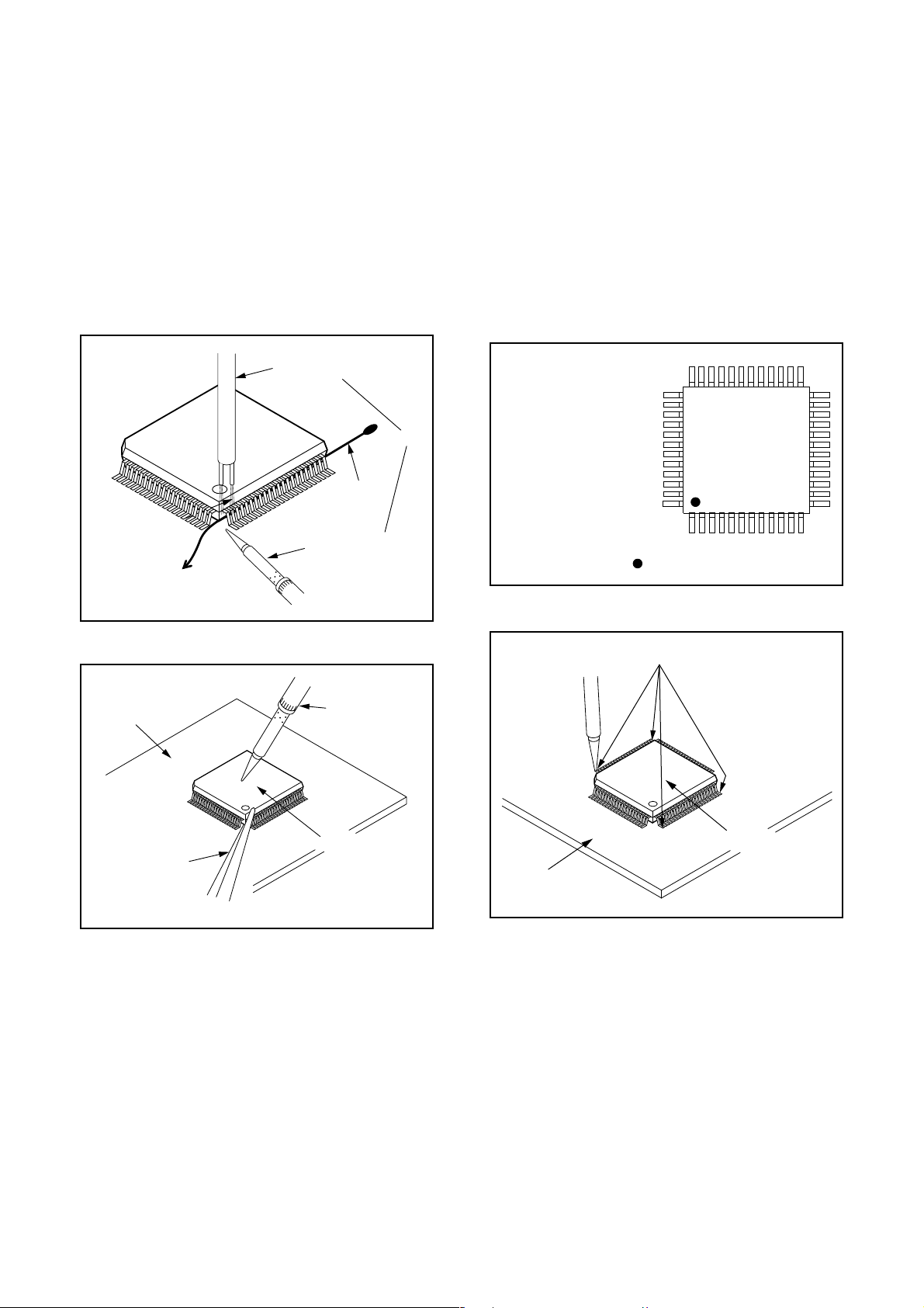
(4) Bottom of the flat pack-IC is fixed with glue to the
CBA; when removing entire flat pack-IC, first apply
soldering iron to center of the flat pack-IC and heat
up. Then remove (glue will be melted). (Fig. S-1-6)
(5) Release the flat pack-IC from the CBA using twee-
zers. (Fig. S-1-6)
Note:
When using a soldering iron, care must be taken
to ensure that the flat pack-IC is not being held by
glue. When the flat pack-IC is removed from the
CBA, handle it gently because it may be damaged
if force is applied.
2. Installation
(1) Using desoldering braid, remove the solder from
the foil of each pin of the flat pack-IC on the CBA so
you can install a replacement flat pack-IC more
easily.
(2) The “ I ” mark on the flat pack-IC indicates pin 1.
(See Fig. S-1-7.) Be sure this mark matches the 1
on the PCB when positioning for installation. Then
presolder the four corners of the flat pack-IC. (See
Fig. S-1-8.)
(3) Solder all pins of the flat pack-IC. Be sure that none
of the pins have solder bridges.
To Solid
Mounting Point
CBA
Hot Air Blower
Iron Wire
Soldering Iron
Fig. S-1-5
Fine Tip
Soldering Iron
or
Example :
Pin 1 of the Flat Pack-IC
is indicated by a " " mark.
Presolder
Fig. S-1-7
Tweezers
Flat Pack-IC
Fig. S-1-6
Flat Pack-IC
CBA
Fig. S-1-8
1-3-3 NOTE_1
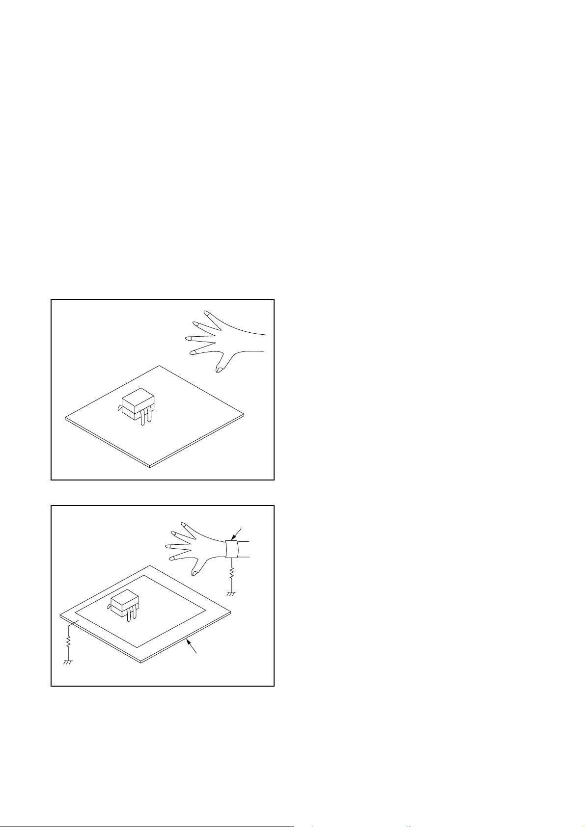
Instructions for Handling
Semi-conductors
Electrostatic breakdown of the semi-conductors may
occur due to a potential difference caused by electrostatic charge during unpacking or repair work.
1. Ground for Human Body
Be sure to wear a grounding band (1MΩ) that is properly grounded to remove any static electricity that may
be charged on the body.
2. Ground for Workbench
Be sure to place a conductive sheet or copper plate
with proper grounding (1MΩ) on the workbench or
other surface, where the semi-conductors are to be
placed. Because the static electricity charge on clothing will not escape through the body grounding band,
be careful to avoid contacting semi-conductors with
your clothing.
<Incorrect>
<Correct>
1MΩ
CBA
Grounding Band
1MΩ
CBA
Conductive Sheet or
Copper Plate
1-3-4 NOTE_1

FUNCTION INDICATOR SYMBOLS
Note:
If a mechanical malfunction occurs, the power is turned off. When the power comes on again after that by
pressing [STANDBY-ON] button, an error message is displayed on the TV screen for 5 seconds.
MODE INDICATOR ACTIVE
When reel or capstan mechanism is not
functioning correctly
When tape loading mechanism is not functioning correctly
When cassette loading mechanism is not
functioning correctly
When the drum is not working properly
P-ON Power safety detection
“EJECT R” is displayed on a TV screen. (Refer to Fig. 1.)
“EJECT T” is displayed on a TV screen. (Refer to Fig. 2.)
“EJECT C” is displayed on a TV screen. (Refer to Fig. 3.)
“EJECT D” is displayed on a TV screen. (Refer to Fig. 4.)
“EJECT P” is displayed on a TV screen. (Refer to Fig. 5.)
TV screen
When reel or capstan mechanism is not functioning
correctly
EJECT R
Fig. 1
When the drum is not working properly
EJECT D
Fig. 4
When tape loading mechanism is not functioning correctly
EJECT T
Fig. 2
When cassette loading mechanism is not functioning
correctly
EJECT C
Fig. 3
P-ON Power safety detection
EJECT P
Fig. 5
1-4-1 H9720FIS
PREPARATION FOR SERVICING
How to Enter the Service Mode
About Optical Sensors
Caution:
An optical sensor system is used for the Tape Start
and End Sensors on this equipment. Carefully read
and follow the instructions below. Otherwise the unit
may operate erratically.
What to do for preparation
Insert a tape into the Deck Mechanism Assembly and
press the PLAY button. The tape will be loaded into
the Deck Mechanism Assembly. Make sure the power
is on, connect TP501 (S-INH) to GND. This will stop
the function of Tape Start Sensor, Tape End Sensor
and Reel Sensors. (If these TPs are connected before
plugging in the unit, the function of the sensors will
stay valid.) See Fig. 1.
Note: Because the Tape End Sensors are inactive, do
not run a tape all the way to the start or the end of the
tape to avoid tape damage.
Q503
TP501 S-INH
Q504
Fig. 1
1-5-1 H9720PFS

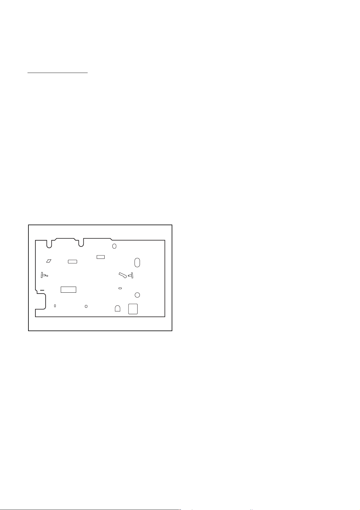
OPERATING CONTROLS AND FUNCTIONS
1-6-1 H9724IB

1-6-2 H9724IB

SIGNAL NAME ABBREVIATIONS
Signal Name Function
-FL FIP Drive Power Supply
8POUT-1
8POUT-2
A-COM Audio Head Common
A-IN Audio Signal Input
A-MODE Hi-Fi Tape Detection Signal
A-MUTE Audio Mute Output
A-MUTE-H
A-OUT Audio Signal Output
A-PB/REC
AE-H Audio Erase Head
AFC
AGC IF AGC Control Signal
AL+12V
AL+2.8V
AL+20.5V
AL+20.5V/
+12V
AL+4.0V
AL+44V
AL+5V
AL+9V
AL-30V
AL-5V
AMPC CTL AMP Connected Terminal
AMPVcc AMPVcc
AMPVREF in V-Ref for CTL AMP
AMPVREF
OUT
ASPECT DVD Aspect Signal
AUDIO+5V +5V at Audio Signal
AVcc
C-CONT Capstan Motor Control Signal
Control SCART 1 8Pin Level by
using 8POUT-1 and 8POUT-2
Control SCART 1 8Pin Level by
using 8POUT-1 and 8POUT-2
Audio Mute Control Signal (Mute =
“H”)
Normal Audio Play Back/Record
Signal
Automatic Frequency Control
Signal
Always +12V with AC Plug
Connected
Always +2.8V with AC Plug
Connected
Always +20.5V with AC Plug
Connected
Always +20.5V/+12V with AC Plug
Connected
Always +4.0V with AC Plug
Connected
Always +44V with AC Plug
Connected
Always +5V with AC Plug
Connected
Always +9V with AC Plug
Connected
Always -30V with AC Plug
Connected
Always -5V with AC Plug
Connected
V-Ref fo r C TL A M P
A/D Converter Power Input/
Standard Voltage Input
Signal Name Function
C-F/R
C-FG
C-POW-SW Capstan Power Switching Pulse
C-ROTA
C-SYNC Composite Synchronized Pulse
CLKSEL Clock Select (GND)
COLOR-IN
CTL(+)
CTL(-) Playback/Record Control Signal (-)
CTLAMPout To Monitor for CTL AMP Output
D-CONT Drum Motor Control Signal
D-PFG
D-REC-H Delayed Record Signal
D-V-SYNC Dummy V-sync Output
DAVN-L VPS/PDC Data Receive = “L”
DISPLAY-CLK VFD Driver IC Control Clock
DISPLAY-DATA VFD Driver IC Control Data
DISPLAY-STB VFD Driver IC Chip Select Signal
DRV-CLK VFD Driver IC Control Clock
DRV-DATA VFD Driver IC Control Data
DRV-STB VFD Driver IC Chip Select Signal
DUBBING-SW Dubbing Start at high
DVD-8P I N - I N
DVD-A DVD Audio Signal
DVD-A( L ) MUTE
DVD-A(R)MUTE
DVD-A-MUTE DVD Audio Mute Control Signal
DVD-A-OUT(L) DVD Audio(L) Signal Output
DVD-AOUT(R)
DVD-B- O U T
DVD-G- O U T
DVD-LED “DVD” LED Signal Output
DVD-OPEN/
CLOSE
Capstan Motor FWD/REV Control
Signal (FWD=”L”/REV=”H”)
Capstan Motor Rotation Detection
Pulse
Color Phase Rotary Changeover
SIgnal
SECAM or MESECAM Chroma
Video Input Signal at Super
Impose
Playback/Record Control Signal
(+)
Drum Motor Phase/Frequency
Generator
SCART 8Pin DVD Input Control
Signal
DVD Audio(L) Mute Control Signal
DVD Audio(R) Mute Control Signal
DVD Audio(R) Signal Output
DVD Component Video Signal
(blue)
DVD Component Video Signal
(green)
DVD Open/Close at High
1-7-1 H9724SNA
Signal Name Function
DVD-P ON+12V
DVD-P ON+3.3V
DVD-P-ON+5V +5V at DVD Power-On Signal
DVD-P L AY DVD Play a t H i gh
DVD-POWER DVD Power Control Signal
DVD-POWERMONITOR
DVD-R - O U T
DVD-STOP DVD Stop at High
DVD-VIDEO DVD Video Control Signal
END-S Tape End Position Detect Signal
EV+1.2V +1.2V Power Supply
EV+11V +11V Power Supply
EV+3.3V +3.3V Power Supply
F1 Filament Power Supply 1
F2 Filament Power Supply 2
FE-H Full Erase Head
FP-CLK Clock Input
FP-DIN Serial Data Input
FP-DOUT Serial Data Output
FP-STB Serial Interface Strobe
FSC-IN
[4.43MHz]
FTV-IN
H-A-COMP Head Amp Comparator Signal
H-A-SW Video Head Amp Switching Pulse
Hi-Fi-A Hi-Fi Audio Head
Hi-Fi-COM Hi-Fi Audio Head Common
Hi-Fi-H-SW HiFi Audio Head Switching Pulse
I/P-SW
IIC-BUS SCL IIC BUS Control Clock
IIC-BUS SDA IIC BUS Control Data
INPUT
SELECT
JK1-16PIN Scart Jack1 16Pin Control Signal
JK1-8P-OUT SCART 8Pin Output Control Signal
JK2-16P Scart Jack2 16Pin Control Signal
KEY-1 Key Scan Input Signal 1
KEY-2 Key Scan Input Signal 2
LD-SW
LINE-MUTE Audio Mute Control Signal
LM-FWD/REV Loading Motor Control Signal
LP LP
+12V at DVD Power-On Signal
+3.3V at DVD Power-On Signal
DVD Power Monitor Signal (Poff="L", P-on="H")
DVD Component Video Signal
(red)
4.43MHz Clock Input
Comparator Input of Video Signal
for Follow TV
Interlace/Progressive Switching
Signal
Input Selector Control Signal
Deck Mode Position Detector
Signal
Signal Name Function
MOD-A Modulator Audio Output Signal
MOD-V Modulator Video Output Signal
N-A-PB Normal Audio Playback
N-A-REC Normal Audio Recording
OSC Oscillator Input
OSCin Clock Input for letter size
OSCout Clock Output for letter size
OSD-V-IN OSD Video Signal Input
OSD-V-OUT OSD Video Signal Output
OSDVcc OSDVcc
OUTPUTSELECT
P-DOWN-L
P-ON+15V +15V at Power-On Signal
P-ON+3.3V +3.3V at Power-On Signal
P-ON+44V +44V at Power-On Signal
P-ON+5V +5V at Power-On Signal
P-ON-H Power On Signal at High
P80/C P80/C Terminal
PB-H-OUT Playback Signal Output at High
PG-DELAY
POW-SAF P-ON Power Detection Input Signal
POWER-LED “POWER” LED Signal Output
PWRCON Power Down
REC-SAF-SW
REMOTE-DVD DVD Remote Control Sensor
REMOTEVIDEO
RESET System Reset Signal (Reset=”L”)
RF-SW Video Head Switching Pulse
RGBTHROUGH
S-REEL Supply Reel Rotation Signal
SC2-IN Input Signal from Pin 8 of SCART2
SIF Source Input Format
SPDIF
ST-S Tape Start Position Detector Signal
T-REEL Take Up Reel Rotation Signal
TIMER+5V +5V at Timer
TU-AUDIO Tuner Audio Input Signal
TU-VIDEO Tuner Video Input Signal
V(L) Video L Head
V(R) Video R Head
V-COM Video Head Common
Output Select
Power Voltage Down Detector
Signal
Video Head Switching Pulse
Signal Adjusted Voltage
Recording Safety SW Detect (With
Record tab=”L”/ With out Record
tab=”H”)
Remote Control Sensor
SCART 2 RGB Through Control
Signal
Digital Audio Interface Format
Signal
1-7-2 H9724SNA

Signal Name Function
V-ENV Video Envelope Comparator Signal
V-IN Video Signal Input
V-IN-F Video Signal Input (Front)
V-OUT Video Signal Output
Vcc Vcc
VCR-LED “VCR” LED Signal Output
VDD Power Supply
VEE Pull Down Level
VIDEO-B Component Video (blue) Signal
VIDEO-C
VIDEO-G Component Video (green) Signal
VIDEO-R Component Video (red) Signal
VIDEO-Y
Vss Vss(GND)
XCin Sub Clock
XCOUT Sub Clock
Xin Main Clock Input
Xout Main Clock Input
Composite Video (chrominance)
Signal
Composite Video (Luminance)
Signal
1-7-3 H9724SNA

CABINET DISASSEMBLY INSTRUCTIONS
1. Disassembly Flowchart
This flowchart indicates the disassembly steps to gain
access to item(s) to be serviced. When reassembling,
follow the steps in reverse order. Bend, route, and
dress the cables as they were originally.
[1] Top Case
[2] Front Assembly
[3] Top Bracket
[4] DVD Mecha Assembly [8] DVD Main CBA Unit
[5] Partition Plate
[6] Power Supply CBA
[7] Loader Holder
[9] VCR Chassis Unit
[10] Deck Assembly
[11] DVD Open/Close CBA
[12] Power SW CBA
[13] Main CBA
[14] Jack-A CBA
REMOVAL
ID/
LOC.
No.
[7]
[8]
[9]
[10]
[11]
[12]
[13] Main CBA D6 ---------- -
[14]
PAR T
Loader
Holder
DVD Main
CBA Unit
VCR
Chassis
Unit
Deck
Assembly
DVD
Open/
Close
CBA
Pow er S W
CBA
Jack-A
CBA
REMOVE/*UNHOOK/
Fig.
UNLOCK/RELEASE/
No.
UNPLUG/DESOLDER
D3 2(S-6) -
2(S-7), *CN201,
D4
*CN301
5(S-8), 2(S-9),
D5
2(S-10), (L-3)
Desolder,
D6
2(S-11), (S-12)
D6 Desolder -
D6 Desolder -
D6 Desolder, 2(S-13) -
Note
2
2-1
2-2
3
-
4,5
2. Disassembly Method
REMOVAL
ID/
LOC.
No.
[1] Top Case D1 8(S-1) -
[2]
[3]
[4]
[5]
[6]
PAR T
Front
Assembly
Top
Bracket
DVD
Mecha
Assembly
Partition
Plate
Power
Suppy
CBA
REMOVE/*UNHOOK/
Fig.
UNLOCK/RELEASE/
No.
UNPLUG/DESOLDER
D2 *3(L-1), *3(L-2)
D2 3(S-2) -
4(S-3), *CN401,
D3
*CN601
D3 (S-4) -
D3 2(S-5), CN501 -
Note
1
1-1
1-2
-
↓
(1)
Note:
(1): Identification (location) No. of parts in the figures
(2): Name of the part
(3): Figure Number for reference
(4): Identification of parts to be removed, unhooked,
unlocked, released, unplugged, unclamped, or
desoldered.
P=Spring, L=Locking Tab, S=Screw,
CN=Connector
*=Unhook, Unlock, Release, Unplug, or Desolder
e.g. 2(S-2) = two Screws (S-2),
2(L-2) = two Locking Tabs (L-2)
(5): Refer to “Reference Notes.”
↓
(2)
↓
(3)
↓
(4)
↓
(5)
1-8-1 H9720DC

Reference Notes
CAUTION 1: Locking Tabs (L-1) and (L-2) are fragile.
Be careful not to break them.
1-1. Release three Locking Tabs (L-1).
1-2. Release three Locking Tabs (L-2), then remove
the Front Assembly.
CAUTION 2: Electrostatic breakdown of the laser
diode in the optical system block may occur as a
potential difference caused by electrostatic charge
accumulated on cloth, human body etc, during
unpacking or repair work.
To avoid damage of pickup follow next procedures.
2-1. Disconnect Connector (CN301). Remove two
Screws (S-7) and lift the DVD Main CBA Unit.
(Fig. D4)
2-2. Short the three short lands of FPC cable with sol-
der before removing the FFC cable (CN201) from
it. If you disconnect the FFC cable (CN201), the
laser diode of pickup will be destroyed. (Fig. D4)
CAUTION 3: When reassembling, confirm the FFC
cable (CN201) is connected completely. Then remove
the solder from the three short lands of FPC cable.
(Fig. D4)
4. When reassembling, solder wire jumpers as shown
in Fig. D6.
5. Before installing the Deck Assembly, be sure to
place the pin of LD-SW on Main CBA as shown in
Fig. D6. Then, install the Deck Assembly while
aligning the hole of Cam Gear with the pin of LDSW, the shaft of Cam Gear with the hole of LD-SW
as shown in Fig. D6.
(S-1)
(L-1)
(S-1)
[1] Top Case
(S-1)
(S-1)
Fig. D1
(S-2)
[3] Top Blacket
(S-2)
(L-1)
[2] Front
(L-2)
Assembly
Fig. D2
1-8-2 H9720DC

[4] DVD Mecha
Assembly
[5] Partition Plate
(S-6)
[7] Loader
Holder
(S-3)
CN501
CN401
CN601
(S-4)
[6] Power
Supply CBA
(S-3)
(S-5)
(S-3)
(S-8)
(S-10)
(S-8)
(S-10)
(S-9)
(S-8)
(S-9)
[9] VCR Chassis Unit
(L-3)
(S-7)
[8] DVD Main
CBA Unit
CN301
A
DVD Mecha
Short the three short lands by soldering.
(Either of two places.)
Fig. D5
Fig. D3
(S-7)
CN201
Connector
View for A
Fig. D4
1-8-3 H9720DC

[10] Deck
Assembly
FE Head
Cylinder
Assembly
ACE Head
Assembly
Pin
Lead with blue stripe
Desolder
[12] Power
SW CBA
[13] Main CBA
[11] DVD
Open/Close CBA
(S-11)
Lead with blue stripe
[14] Jack-A CBA
(S-11)
(S-13)
Desolder
from bottom
(S-12)
Desolder
Lead with
blue stripe
From
ACE Head
Assembly
Lead with
blue stripe
[13] Main CBA
[10] Deck Assembly
Shaft
Hole
LD-SW
From
Cylinder
Lead with
blue stripe
Assembly
Desolder
From
FE Head
SW507
LD-SW
Cam Gear
Hole
Pin
[13] Main CBA
Lead with
red stripe
Desolder
Printing side
From
Capstan
Motor
Assembly
Desolder
BOTTOM VIEW
Lead connections of Deck Assembly and Main CBA
1-8-4 H9720DC
Fig. D6

HOW TO EJECT MANUALLY
1. Remove the Top Case.
2. Rotate the roulette in the direction of the arrow as
shown below.
3. Pull the tray slowly with a hand.
View for A
Rotate this roulette in
the direction of the arrow
DVD Mecha
A
1-8-5 H9720DC

ELECTRICAL ADJUSTMENT INSTRUCTIONS
c
General Note: "CBA" is an abbreviation for
"Circuit Board Assembly."
NOTE:
1.Electrical adjustments are required after replacing
circuit components and certain mechanical parts.
It is important to do these adjustments only after
all repairs and replacements have been completed. Also, do not attempt these adjustments
unless the proper equipment is available.
2.To perform these alignment / confirmation proce-
dures, make sure that the tracking control is set in
the center position: Press either "CHANNEL L 5??" or
"CHANNEL K" button on the front panel first, then
the "PLAY" button on the front panel.
Test Equipment Required
1.Oscilloscope: Dual-trace with 10:1 probe,
V-Range: 0.001~50V/Div.,
F-Range: DC~AC-20MHz
2.Alignment Tape (9965 000 14514)
Head Switching Position Adjustment
Figure 1
EXT. Syncronize Trigger Point
CH1
CH2
Reference Notes:
Playback the Alignment tape and adjust VR501 so that
the V-sync front edge of the CH1 video output waveform is at the 6.5H±1H (416µs±64µs) delayed position
from the rising edge of the CH2 head switching pulse
waveform.
1.0H
6.5H±1H (416µs±64µs)
Switching Pulse
0.5H
V-Syn
Purpose:
To determine the Head Switching position during
playback.
Symptom of Misadjustment:
May cause Head Switching noise or vertical jitter
in the picture.
Test point Adj.Point Mode Input
TP751(V-OUT)
TP504(RF-SW)
GND
Tape
9965 000 14514 Oscilloscope
Connections of Measurement Equipment
Main CBA
VR501
(Switching Point)
(MAIN CBA)
Measurement
Equipment
TP751
GND
TP504
PLAY
(SP)
Spec.
6.5H±1H
(416µs±64µs)
Oscilloscope
-----
CH1 CH2
Trig. (+)
1-9-1 H9720EA
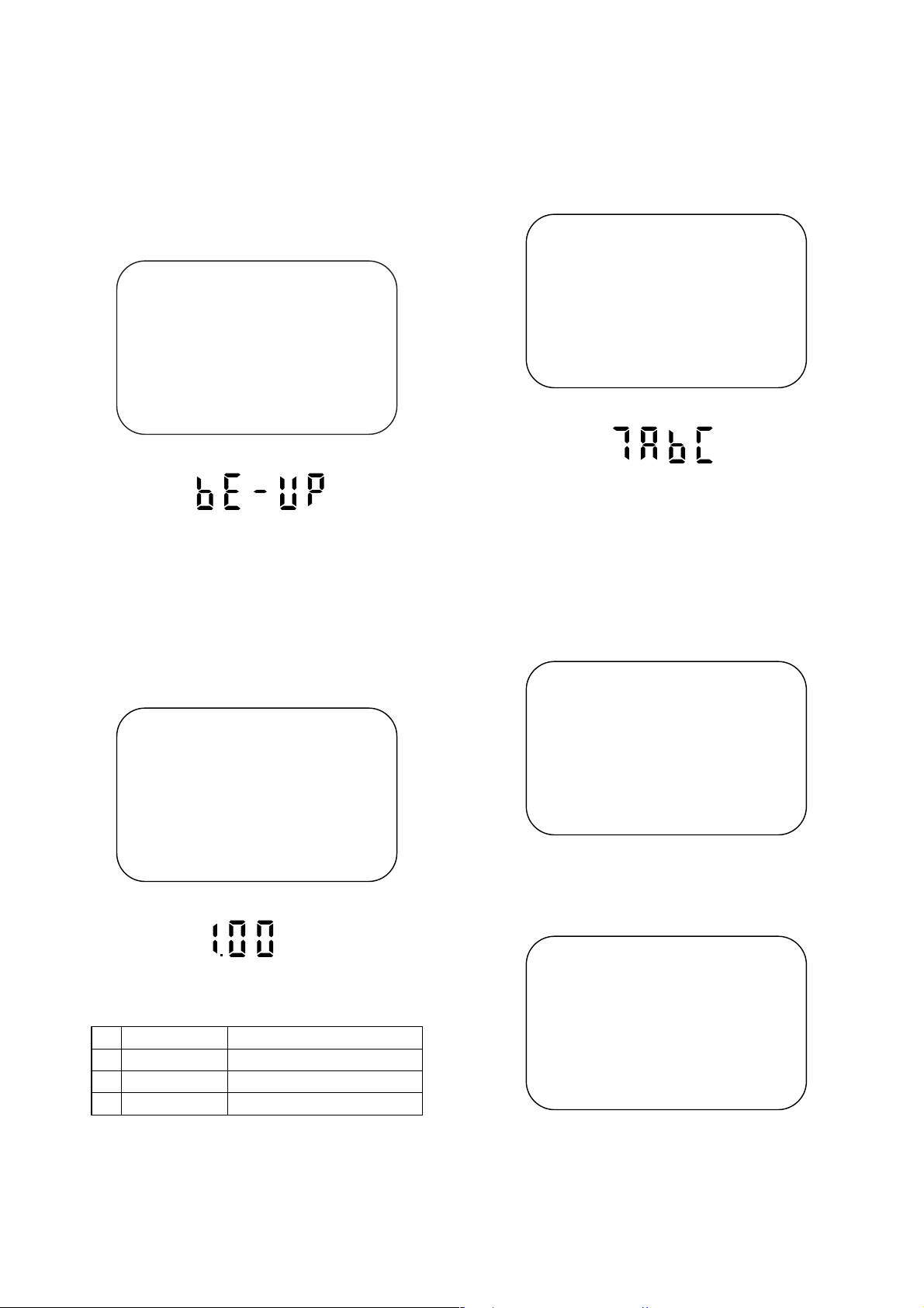
FIRMWARE RENEWAL MODE
1. Turn the power on and remove the disc on the tray.
2. To put the DVD player into version up mode, press
[9], [8], [7], [6], and [SEARCH MODE] buttons on
the remote control unit in that order. The tray will
open automatically.
Fig. a appears on the screen and Fig. b appears on
the VFD.
"
" differ depending on the models.
*******
F/W Version Up Mode Model No : *******
Please insert a DISC
for F/W Version Up.
VERSION : *.**
EXIT: POWER
Fig. a Version Up Mode Screen
Fig. b VFD in Version Up Mode
The DVD player can also enter the version up
mode with the tray open. In this case, Fig. a will be
shown on the screen while the tray is open.
3. Load the disc for version up.
4. The DVD player enters the F/W version up mode
automatically. Fig. c appears on the screen and
Fig. d appears on the VFD. If you enter the F/W for
different models, “Disc Error” will appear on the
screen, then the tray will open automatically.
"
" differ depending on the models.
*******
F/W Version Up Mode Model No : *******
VERSION : D5****_****.ab5
Reading...(*1)
VERSION : *.**
5. After programming is finished, the tray opens automatically. Fig. e appears on the screen and the
checksum in (*2) of Fig. e appears on the VFD.
(Fig. f)
"
" differ depending on the models.
*******
F/W Version Up Mode
VERSION : D5****_****.ab5
Completed
SUM : 7ABC (*2)
Model No : *******
VERSION : *.**
Fig. e Completed Program Mode Screen
Fig. f VFD upon Finishing the Programming Mode (Example)
At this time, no buttons are available.
6. Remove the disc on the tray.
7. Unplug the AC cord from the AC outlet. Then plug it
again.
8. Turn the power on by pressing the [STANDBY-ON]
button and the tray will close.
9. Press [1], [2], [3], [4], and [DISPLAY/STATUS] buttons on the remote control unit in that order.
Fig. g appears on the screen.
"
" differ depending on the models.
*******
MODEL : *******
Version
Region
: *.**
: *
Fig. c Programming Mode Screen
Fig. d VFD in Programming Mode (Example)
The appearance shown in (*1) of Fig. c is
described as follows:
AppearanceNo. State
Reading... Sending files into the memory
1
Erasing... Erasing previous version data
2
Programming...
3 Writing new version data
EXIT: POWEREEPROM CLEAR : CLEAR
Fig. g
10.Press [CLEAR/C-RESET] button on the remote
control unit.
Fig. h appears on the screen.
"
" differ depending on the models.
*******
MODEL : *******
Version
Region
: *.**
: *
EXIT: POWEREEPROM CLEAR : CLEAR
EEPROM CLEAR : OK
Fig. h
When “OK” appears on the screen, the factory
default will be set. Then the firmware renewal mode
is complete.
11.To exit this mode, press [STANDBY-ON] button.
1-10-1 H9720TEST

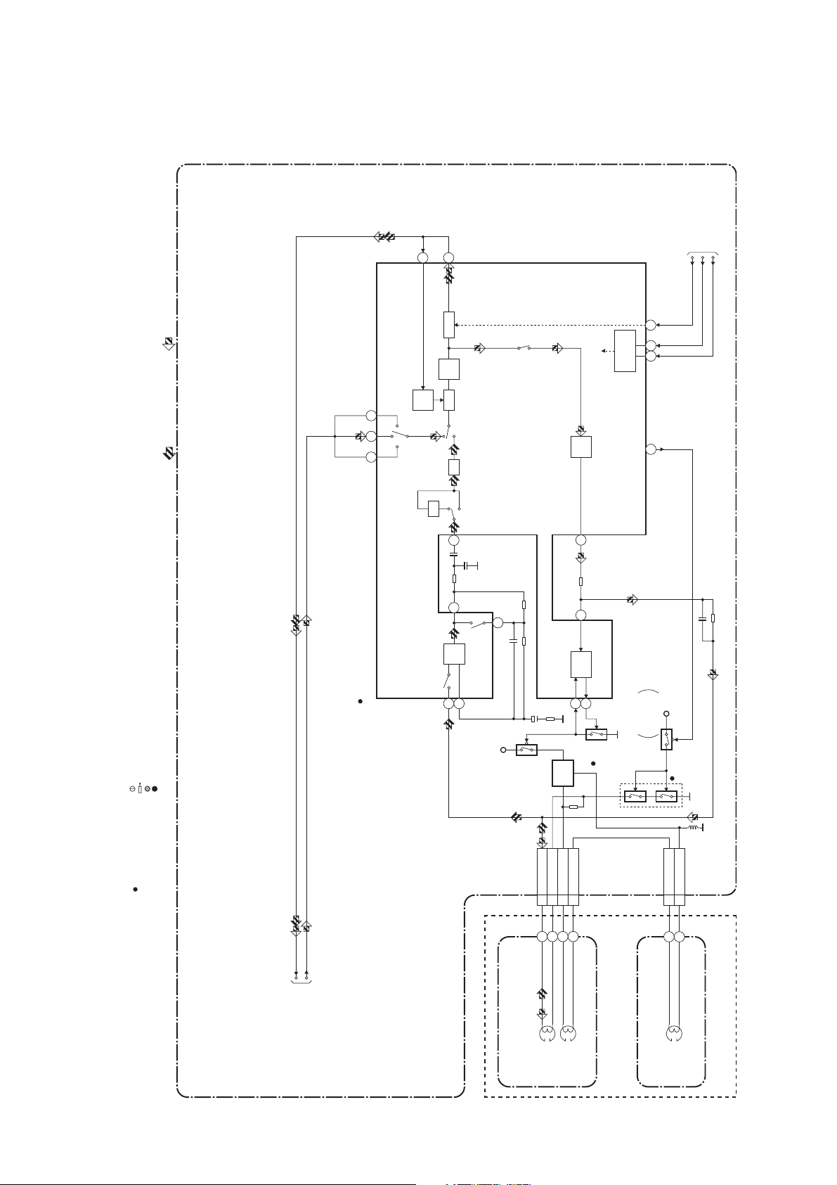
BLOCK DIAGRAMS <VCR SECTION>
Servo/System Control Block Diagram
AL+5V
D651
POWER
CN508
POWER
TO AUDIO
BLOCK DIAGRAM
SW651
POWER SW CBA
TO Hi-Fi AUDIO
BLOCK DIAGRAM
TO DVD
VIDEO/AUDIO
BLOCK DIAGRAM
<DVD SECTION>
TO VIDEO
BLOCK DIAGRAM
TO DVD SYSTEM
CONTROL BLOCK
DIAGRAM
<DVD SECTION>
CN509
TP501
SENS-INH
KEY SWITCH
8
KEY- 2
LD-SW
IC501
(SERVO/SYSTEM CONTROL)
9
:USED TO INDICATE A TEST POINT WITH NO TEST PIN.
:USED TO INDICATE A TEST POINT WITH A TEST PIN.
MAIN CBA
:INDICATES A TEST POINT WITH A JUMPER WIRE ACROSS A HOLE IN THE PCB.
:USED TO INDICATE A TEST POINT WITH A COMPONENT LEAD ON FOIL SIDE.
TEST POINT INFORMATION
T-REEL
S-REEL79
D502
Q515
PS502
IC502 (MEMORY)
DVD
Q508
RESET
34
RESET
TIMER+5V
S-REEL
POWER-LED
11KEY-1
33
KEY SWITCH
Q507
7
23
KEY- 1
POWER-LED
ST-S
END-S
CTL(+)
CTL(-)
949510480
SDA
SCL
IIC-BUS SDA
5
6
AL+5V
D503
VCR
Q509
29
30
DVD-LED
VCR-LED
REMOTE-VIDEO
DRV-DATA
DRV-STB
DRV-CLK
14
68
69
70
REMOTE-VIDEO
DISPLAY-DATA
DISPLAY-STB
DISPLAY-CLK
TO DVD SYSTEM
CONTROL BLOCK
DIAGRAM
<DVD SECTION>
A-MUTE-H
IIC-BUS SCL
IIC-BUS SDA
83
A-MUTE-H
P-ON+5V
IC775
(COMPARATOR)
A-MODE
Hi-Fi-H-SW
IIC-BUS SCL
32
19
A-MODE
Hi-Fi-H-SW
FTV-IN
2 64
4
AND
Q775,
Q776
14
9
8
LINE-MUTE
OUTPUT SELECT
OUTPUT SELECT
28
LINE-MUTE
5
13
11
10
TP503
AL+5V
CTL97
CTL
DAVN-L
D-REC-H
IIC-BUS SCL
IIC-BUS SDA
71
56
72
DAVN-L
IIC-BUS SCL
IIC-BUS SDA
REC-SAF-SW
PG-DELAY
2
31
AL+5V
VR501
SW-POINT
RF-SW
C-ROTA
15
18
33
RF-SW
C-ROTA
D-REC-H
SW506
REC-SAFETY
CN502
V-ENV
H-A-SW
D-V-SYNC
H-A-COMP
13
17
16
H-A-SW
D-V-SYNC
H-A-COMP
C-FG
87
P-ON+5V
AL+20.5V/+12V
AL+20.5V/+12V
1
2 P-ON+5V
3 C-FG
C-SYNC
INPUT-SELECT
OUTPUT-SELECT
6
58C-SYNC
41
82
V-ENV
INPUT-SELECT
OUTPUT-SELECT
C-CONT
LM-FWD/REV
D-CONT77
76
81
D-CONT9D-PFG10GND11AL+12V(2)12P-ON+15V
8
D-PFG
90
C-F/R
78
C-F/R5C-CONT6GND7LM-FWD/REV
4
DVD-PLAY
DVD-POWER
OUTPUT-SELECT
12
21
DVD-PLAY
DVD-POWER
P-ON-H
C-POW
-SW
67
66
AL+12V(2)
P-ON+15V
P-ON-H
C-POW-SW
P-DOWN-L
TO POWER
SUPPLY BLOCK
86 P-DOWN-L
DIAGRAM
" " = SMD
SW507
(DECK ASSEMBLY)
LD-SW
AC HEAD
AL+5V
CN504
CL504
2 CTL(+)
1 CTL(-)
ASSEMBLY
CONTROL
HEAD
AL+5V
TP502
Q506
END-S
T-REEL
S-LED
D555
Q504
P-ON+5V
ST-S
TU-
VIDEO
TO VIDEO
BLOCK
SENSOR CBA
1-11-1
V-IN1
DIAGRAM
END-S
Q503
SENSOR CBA
M
CAPSTAN MOTOR
CAPSTAN
MOTOR
M
PG
SENSOR
DRUM
CYLINDER ASSEMBLY
MOTOR
M
LOADING
MOTOR
H9724BLS

Video Block Diagram
MODE: SP/RECPB-VIDEO SIGNAL DVD VIDEO SIGNAL
MAIN CBA
VIDEO (L)-1
HEAD
VIDEO (R)-1
HEAD
CYLINDER ASSEMBLY
(DECK ASSEMBLY)
456
123
V(L)-2
V(L)-1
CN251
V(R)-1
V-COM
VIDEO (R)-2
VIDEO (L)-2
HEAD
V(R)-2
V-COM
HEAD
WF1
RF-SW
TP504
RF-SW
D-REC-H
C-ROTA
TO SERVO/SYSTEM
CONTROL BLOCK
DIAGRAM
V-ENV
H-A-SW
C-SYNC
D-V-SYNC
H-A-COMP
REC-VIDEO SIGNAL
TO SERVO/SYSTEM
CONTROL BLOCK
DIAGRAM
DAVN-L
IIC-BUS SCL
IIC-BUS SDA
:INDICATES A TEST POINT WITH A JUMPER WIRE ACROSS A HOLE IN THE PCB.
:USED TO INDICATE A TEST POINT WITH A COMPONENT LEAD ON FOIL SIDE.
:USED TO INDICATE A TEST POINT WITH NO TEST PIN.
:USED TO INDICATE A TEST POINT WITH A TEST PIN.
TEST POINT INFORMATION
" " = SMD
6147
16
VPS-V
DAVN-L
IIC-BUS SCL
IIC-BUS SDA
IC631 (VPS)
55
50
COLOR
OSD
CHARACTER
MIX
IC501 (OSD)
52
TU-VIDEO
V-IN1
TO SERVO/SYSTEM
CONTROL BLOCK
DIAGRAM
7978
46 43
6968
65
-IN
IC301
(Y/C SIGNAL PROCESS)
6
24
VIDEO
TU-VIDEO
(TUNER UNIT)
TU701
Y. DELAY
SERIAL
DECORDER
4
(INPUT SELECT)
IC1404
5
3
JK752
V-IN
FRONT
969594
SP
HEAD
AMP
EP
SP
P
R
LUMINANCE
SIGNAL
PROCESS
AGC
BYPASS
IN1
IN2
TUNER
485052
9
SW CTL
93
FRT
IN2
56
54
TO
908988
87
EP
HEAD
AMP
REC FM
AGC
+
Y
CCD 1H DELAY
1/2
CHARA.
INS.
FRT
MUTE
PB/EE
IN1
TUNER
INPUT-SELECT
DVD-VIDEO
SERVO/SYSTEM
CONTROL BLOCK
DIAGRAM
TO DVD
VIDEO/AUDIO
BLOCK DIAGRAM
62
70
80
D-REC-H
D-V-SYNC
RF-SW/C-ROTA
C
CHROMINANCE
SIGNAL
PROCESS
FBC
MUTE
PB/EE
JK101
19
20
V-OUT1
<DVD SECTION>
83
71
H-A-SW
H-A-COMP
RPRP
V-IN1
67
84
V-ENV
C-SYNC
Y/C
PR
MIX
AGC VXO
61
63
8
CN2017
V-OUT2
8
CN2018
BUFFER
JK1402
19
V-OUT2
V-IN2
10 10
Q103
20
V-IN2
21
2928
58 59
BUFFER
Q104
JACK-A CBA
WF2
C-PB
TP301
X301
4.43MHz
3
5
DVD
VCR
IC751
(OUTPUT SELECT)
4
TO SERVO/SYSTEM
CONTROL BLOCK DIAGRAM
OUTPUT-SELECT
11109
SW CTL
WF3
V-OUT
TP751
1-11-2
H9724BLV
Audio Block Diagram
Mode : SP/REC
ALC
TO SERVO/SYSTEM
CONTROL BLOCK
11
12
SERIAL
DECODER
71
68 69
DET
LINE
MUTE
AMP
ALC
REC-ON
DIAGRAM
A-MUTE-H
IIC-BUS SCL
IIC-BUS SDA
PB-AUDIO SIGNAL REC-AUDIO SIGNAL
MAIN CBA
:INDICATES A TEST POINT WITH A JUMPER WIRE ACROSS A HOLE IN THE PCB.
:USED TO INDICATE A TEST POINT WITH A COMPONENT LEAD ON FOIL SIDE.
:USED TO INDICATE A TEST POINT WITH NO TEST PIN.
:USED TO INDICATE A TEST POINT WITH A TEST PIN.
TEST POINT INFORMATION
IC301
IN1
1513 17
(AUDIO SIGNAL PROCESS)
P
R
INV
PB-ON
ATT
98
7
EQ
AMP
SP/LP-ON
5
6
+5V
Q404
TUNER IN2
Q403
BIAS
OSC
REC
AUTO
1
AMP
100
3
BIAS
2
Q406
16
AUDIO HD-SW
CONTROL
SWITCHING
D-REC-OFF
Q405
+5V
Q401
(PB=ON)
" " = SMD
N-A-PB
N-A-REC
TO Hi-Fi AUDIO
BLOCK DIGRAM
1-11-3
CN504
4 A-PB/REC
3 A-COM
AC HEAD ASSEMBLY
AUDI O
HEAD
(DECK ASSEMBLY)
1 AE-H
2 AE-H/FE-H
AUDI O
ERASE
HEAD
CN501
2 FE-H
1 FE-H-GND
FE HEAD
FULL
ERASE
HEAD
H9724BLA

Hi-Fi Audio Block Diagram
TO
SERVO/ SYSTEM
CONTROL BLOCK
DIAGRAM
TO DVD VIDEO/
DVD-A-OUT(R)
DVD AUDIO SIGNAL
OUTPUT-SELECT
AUDIO BLOCK
DIAGRAM
<DVD SECTION>
DVD-A-OUT(L)
IIC-BUS SDA
IIC-BUS SCL
A-MODE
TO
SERVO/ SYSTEM
CONTROL BLOCK
DIAGRAM
Hi-Fi-H-SW
LINE-MUTE
Hi-Fi
AUDIO
(R)
HEAD
CYLINDER
ASSEMBLY
(DECK ASSEMBLY)
CN251
Hi-Fi-A(L) 9
Hi-Fi-A(R) 7
Hi-Fi-COM 8
Hi-Fi
AUDIO
(L)
HEAD
REC-AUDIO SIGNALPB-AUDIO SIGNAL Mode : SP/REC
VCR
IC751
(OUTPUT SELECT)
MAIN CBA
Q451
37
2
DVD
14
1
13
DVD
15
Q107
Q152 Q154
Q153
A-MUTE(L)
11109
SW CTL
Q108
BUFFER
BUFFER
A-MUTE(R)
Q151
Q155
SERIAL
R-CH
BPF
COMP
SW
NOISE
SW
ALC
ALC
SW
IC451 (MTS/ SAP/ Hi-Fi AUDIO PROCESS/ Hi-Fi HEAD AMP)
67
65
VCR
12
38
DATA
DECODER
P
R-CH
62 70
21
ENV
DO
LPF
VCO
LIM DEV
R
PNR
61 71
DET
DET
MUTE-ON
47
48
R-CH
52
56
767774
OUTPUT
INSEL
50
54
MUTE-ON
SELECT
60
58
39
26
53
75
73
COMP
MIX
HOLD
PULSE
NOISE
DET
15
14
L-CH
INSEL
2
6
4
8
12
10
LPF
VCO
LIM DEV
R
L-CH
24
R
P
PNR
NOR
34 33
LIM
L-CH
COMP
SW
SW
27
L
BPF
NOISE
78
80
:INDICATES A TEST POINT WITH A JUMPER WIRE ACROSS A HOLE IN THE PCB.
:USED TO INDICATE A TEST POINT WITH A COMPONENT LEAD ON FOIL SIDE.
:USED TO INDICATE A TEST POINT WITH NO TEST PIN.
:USED TO INDICATE A TEST POINT WITH A TEST PIN.
5
4
1
TEST POINT INFORMATION
" " = SMD
CN2017CN2018
A-IN2(R)
4
A-OUT2(R)
A-IN2(L)
5
1
JACK-A CBA
JK1402
2
6
1
A-OUT2(R)
A-IN2(R)
A-IN2(L)
TO DVD VIDEO/AUDIO
BLOCK DIAGRAM
<DVD SECTION>
2
A-OUT2(L)
2
3
A-OUT2(L)
JK101
2
1
3
A-IN1(R)
A-OUT1(R)
A-OUT1(L)
6
A-IN1(L)
JK751
A-OUT(R)
REAR
A-OUT(L)
1-11-4
Q753 Q754
JK753
A-IN(L)
FRONT
JK754
A-IN(R)
2
AUDIO
TU701
(TUNER UNIT)
4
CN701CN1
TU-AUDIO(R)
4
AFV CBA
IF SINAL
2
SIF
2
CN701 CN1
22
SIF
5
TU-AUDIO(L)
5
PROCESS
N-A-REC
N-A-PB
TO AUDIO
BLOCK DIAGRAM
H9724BLH

Power Supply Block Diagram
1 EV+1.2V
CL1051
2 EV+1.2V
3 EV+3.3V
4 EV+3.3V
5 EV+3.3V
7 P-ON+5V
8 EV+11V
9 EV+11V
6 P-ON+3.3V
17 PWRCON
P-ON-H
P-ON+44V
SW+44V
Q053,Q054
CAUTION !
Fixed voltage (or Auto voltage selectable ) power supply circuit is used in this unit.
If Main Fuse (F1001) is blown, check to see that all components in the power supply
circuit are not defective before you connect the AC plug to the AC power supply.
Otherwise it may cause some components in the power supply circuit to fail.
P-ON+15V
<FROM PIN 67 OF IC501>
13568
13568
CN051A
1 AL+44V13 AL+12V35
CL051A CL051B CN051
AL+12V
5
AL+5V(P-DOWN)
Q055
8
6 AL+5V68 AL+20.5V
AL+9V
AL+5V
SW+9V
Q056
101214
1012141817
P-ON+5V
Q058
SW+5V
18
17
TIMER+5V
SW+5V
Q057
Q059
C-POW-SW
P-DOWN-L
AL+20.5V/+12V
<TO PIN 86 OF IC501>
<FROM PIN 66 OF IC501>
SW+20.5V
Q051,Q052
AL-30V
1
1 AL-30V
CL052A CL052B
IC1002
+1.2V REG.
359
3 AL+2.8V
5 AL+4V
9 F1
IC1003
+3.3V REG.
8F2
8
SW+5V
Q1055
JUNCTION
Q1052
CBA
SW+3.3V
DVD P-ON+5V
-FL
DVD P-ON+3.3V
Q1053,
DVD P-ON+12V
EV+3.3V
F1
SW+12V
Q1054
F2
MAIN CBAPOWER SUPPLY CBA
CAUTION
FOR CONTINUED PROTECTION AGAINST FIRE HAZARD,
REPLACE ONLY WITH THE SAME TYPE T1.6AL/250V FUSE.
20
19
T0011
2
BRIDGE
RECTIFIER
D001 - D004
NOTE :
The voltage for parts in hot circuit is measured using
hot GND as a common terminal.
HOT CIRCUIT. BE CAREFUL.
LINE
L1003
F1001
T1.6AL/250V
AC1001
FILTER
COLD
Q1004
18
17
16
15
14
13
12
11
4
Q1001
Q1003
7
8
IC1001
ERROR
VOLTAGE DET
1
4
23
Q1008
HOT
1-11-5
H9724BLP

BLOCK DIAGRAMS <DVD SECTION>
DVD System Control / Servo Block Diagram
DVD OPEN/CLOSE CBA
IC101
CN2015 CN2016
(MICRO CONTROLLER)
SW2020
DVD OPEN/CLOSE
1
2
DVD-OPEN/CLOSE
EV+3.3V
1
2
EV+3.3V
ADAC-MD
A-MUTE
PCM-SCLK
57
88
163
56 ADAC-MC
86 ADAC-ML
ASPECT
21
EV+3.3V
RESET73
PLAY
SW2022
STOP
SW2021
FD-OFST
FOCUS DRIVE
148
146
FROM SERVO/SYSTEM
CONTROL BLOCK
DIAGRAM
<VCR SECTION>
DVD-PLAY
DVD-POWER
OUTPUT-SELECT
CL1051
DVD-STOP 2626DVD-POWER 2323DVD-OPEN/CLOSE
DVD-PLAY 25
25
CN401
535465
DVD-PLAY
DVD-STOP
DVD-POWER
TRACKING
DRIVE
TD-OFST
147
139
IC612
22
24
FP-STB 2020FP-DIN 1919FP-CLK 18
REMOTE-DVD
18
22
24
82
60
67
59
68
FP-DIN
FP-STB
FP-CLK
REMOTE
DVD-OPEN/CLOSE
SPDL
76
IC611
GRID FIP
~
23
~
1G
(FIP DRIVER)
27
OUTPUT-SELECT
27
55
OUTPUT-SELECT
17
7G
SLD
75
789
a
bcd
10
SP-ROT
143
SEGMENT
12
11
131416
f
e
g
FP-STB
FP-DIN
2281
i
h
FP-CLK
SL-AMP
81
TO SERVO/SYSTEM
CONTROL BLOCK
DISPLAY-CLK
DISPLAY-DATA
REMOTE-VIDEO
REMOTE
RM2001
DIAGRAM
<VCR SECTION>
DISPLAY-STB
SENSOR
TRAY-IN
66
MAIN CBA
SLED SERVO SIGNAL SPINDLE SERVO SIGNAL
FOCUS SERVO SIGNAL TRACKING SERVO SIGNAL
" " = SMD
A-MUTE
ADAC-MD
PCM-SCLK
TO DVD
VIDEO/ AUDIO
ADAC-MC
BLOCK DIAGRAM
ADAC-ML
IC462
+3.3V
ASPECT
RESET
1 3
VREF
IC301
(SERVO DRIVE)
27
-
+
+
FOCUS
ACTUATOR
15
FS(+)
26
FS(-)
-
DRIVE
16
TO DIGITAL SIGNAL
25
24
-
+
-
+
TRACKING
ACTUATOR
DRIVE
14
13
TS(+)
TS(-)
PROCESS BLOCK
DIAGRAM
312
-
+
-
+
SPINDLE
MOTOR
DRIVE
12
11
1
7
14
645
23
IC202
+
SLED
MOTOR
17
-
DRIVE
18
(OP AMP)
3
TRAY-IN
2
6
5
CN301
SPINDLE
MOTOR
+3.3V
3SP(+)
M
4SP(-)
13
12
5TRAY-IN
6GND
SLED
MOTOR
7SL(-)
DVD MAIN CBA UNITDRIVE CBA
8SL(+)
M
1-11-6
H9724BLSD

Digital Signal Process Block Diagram
TO DVD
VIDEO
/AUDIO
BLOCK
DIAGRAM
TO DVD
VIDEO
/AUDIO
BLOCK
DIAGRAM
FLASH
ROM
DATA(AUDIO) SIGNAL
DATA(VIDEO/AUDIO) SIGNAL DVD VIDEO SIGNAL
DATA
RAM
DSP
INST.
ROM
DECODER
STREAM
I/F
DATA
RAM
I/O
INST.
ROM
PROCESSOR
SPDIF
177
PCM-BCK
PCM-DATA
PCM-LRCLK
170
171
AUDIO
I/F
UMAC
169
SERIAL
GENERAL
I/O
INTERRUPT
CPU
I/F
READ
MEMORY
VIDEO-Y
156
Y
D/A
CONTROLLER
VIDEO-C
158
C
D/A
TIMER
WATCH DOG
VIDEO-R
152
R
D/A
NTSC/PAL
ENCODER
VIDEO
I/F
TIMER
REMOTE
VIDEO-B
151
B
D/A
CONTROL
VIDEO-G
149
G
D/A
32BIT CPU
BCU
DATA
INST
DEBUG
RAM
RAM
IC103 (FLASH ROM)
23~51
~
~
1
9
162548
FADR (0-19)
~
293638
FDQ (0-15)
~
45
" " = SMD
IC503 (SDRAM) IC101 (MICRO CONTROLLER)
EXTERNAL
MEMORY
I/F
SDRAM ADDRESS(0-10)
~
217
238
SDRAM ADDRESS(0-11)
~~
222629
35
SDRAM
DECODER
I/F
ECC
SDRAM DATA(0-15)
~~
1
18
252
SDRAM DATA(0-15)
~~
2
134253
256
114
115
116
DMA
DVD/CD
RF
SIGNAL
117
132
CN201
C16
FORMATTER
PROCESS
CIRCUIT
131
134
A17
D18
192~212
CPU
I/F
BCU
WATCH DOG
5
9
GND(LD)
GND(CD-PD)
TIMER
INTERRUPT
TIMER
CONTROLLER
CD/DVD
83
TO DVD SYSTEM
CONTROL/SERVO
BLOCK DIAGRAM
6
IC201
(SW)
4
1 3
CD DVD
FS
TS
FS(+)
CN201
FS(+) 2
FS(-)
FS(-) 3
TS(+)
TS(+) 1
TS(-)
TS(-) 4
DVD MAIN CBA UNIT
PICK-UP
UNIT
32BIT
CPU
INST.
ROM
DATA
RAM
126
124
125
AMP
Q253,Q254
AMP
CN201
CD-LD 10
DVD-LD 8
123
Q251,Q252
6
PD-MONI 7
GND(DVD-PD)
133
129
130
F12
B15
E14
CD/DVD 19
DETECTOR
1-11-7
H9724BLD
 Loading...