

Page 1
Philips Consumer Electronics Company
A Division of Philips Electronics North America Corporation
Se
Technical Service Data
Service Solutions Group
hnical Publications Dept.
Tec
P.O. Box 555
Jefferson City,TN 37760
, 401 E. Old Andrew Johnson Hwy.
c. 1A: Main Section
( DVDR600VR/37, MRV700VR/17 )
Specifications
Opera
Adjustment Proc
Schematic D
loded Views
Exp
Cabin
Sec. 2: Deck Mechanism Section
Sec. 3: DVD+RW Basic Engine
VA
For repair information on the Basic
gine.
En
MANUAL 5903
ting Instructions
edures
iagrams and CBA’s
et & Electrical Parts Lists
D8041 12NC:
3122 785 14850
71/RV007VRMXOVANGAM
DVD Recorder &
Video Cassette Recorder
Service Manual
73/RV006RDVDSPILIHPredroceR ettessaC oediV & redroceR DVD 3095 LAUNAM
PHILIPS
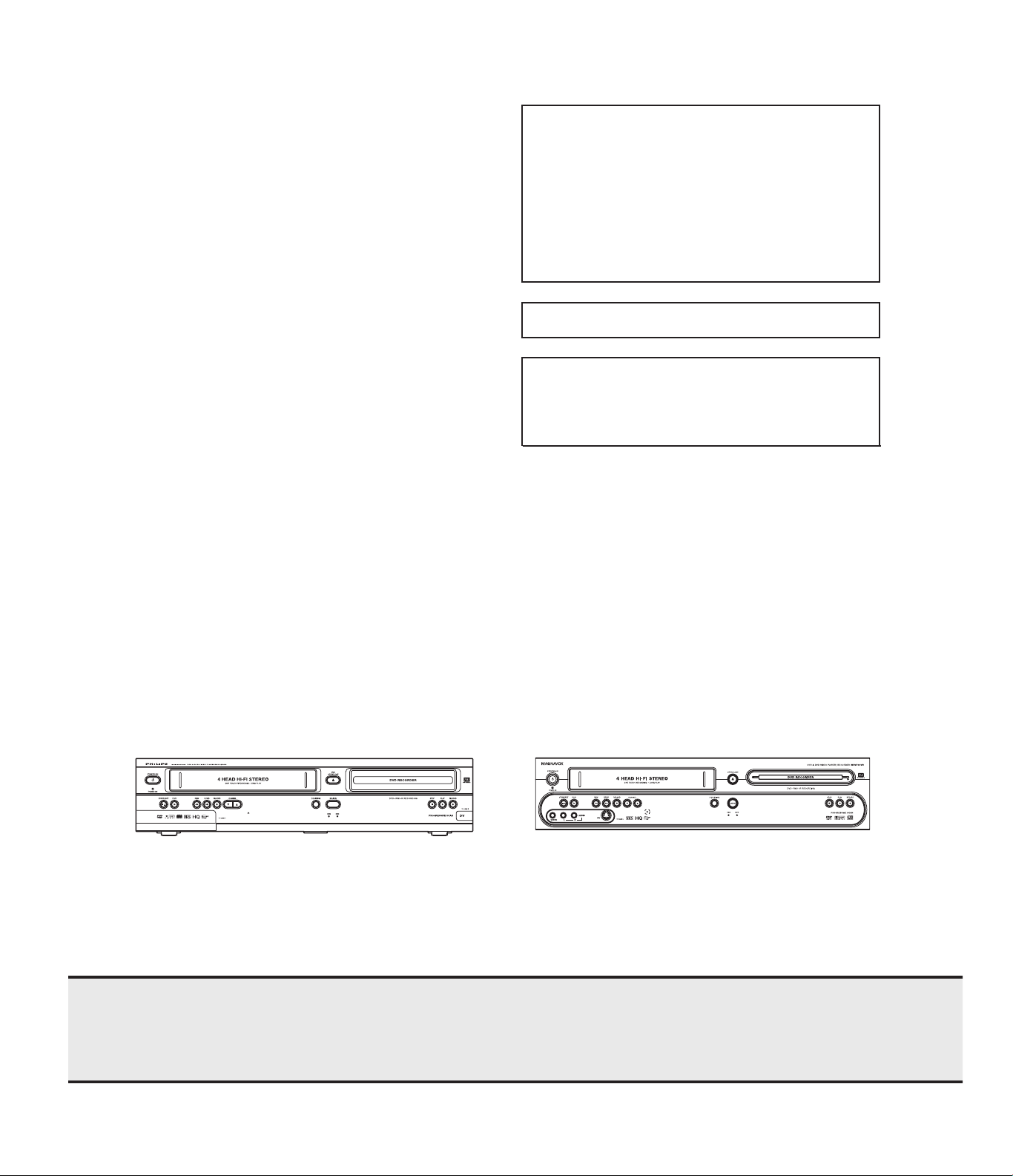
Model: DVDR600VR/37
AGNAVOX
M
Model: MRV700VR/17
DVD Recorder & Video Cassette Recorder
First Issue: 9/04
©2004 Philips Consumer Electronics Company
Page 2
Philips Consumer Electronics Company
A Division of Philips Electronics North America Corporation
Se
Technical Service Data
Service Solutions Group
hnical Publications Dept.
Tec
P.O. Box 555
Jefferson City,TN 37760
, 401 E. Old Andrew Johnson Hwy.
c. 1A: Main Section
( DVDR600VR/37, MRV700VR/17 )
Specifications
Opera
Adjustment Proc
Schematic D
loded Views
Exp
Cabin
MANUAL 5903
ting Instructions
edures
iagrams and CBA’s
et & Electrical Parts Lists
DVD Recorder &
Video Cassette Recorder
Service Manual
PHILIPS
Model: DVDR600VR/37
Model: MRV700VR/17
AGNAVOX
M
DVD Recorder & Video Cassette Recorder
First Issue: 9/04
©2004 Philips Consumer Electronics Company
Page 3

IMPORTANT SAFETY NOTICE
Proper service and repair is important to the safe, reliable operation of all
Philips Consumer Electronics Com pany** Equipment. The service procedures
recommended by Philips and described in this service manual are effective
methods of performing service operations. Some of these service operations
require the use of tools specially designed for the purpose. The special tools
should be used when and as recommended.
It is important to note that this manual contains various CAUTIONS and
NOTICES which should be carefully read in orde r to minimize the risk of personal injury to service personnel. The possibility exists that improper service
methods may damage the equipment. It also is i mportant to understand that
these CAUTIONS and NOTICES ARE NOT EXHAUSTIVE. Philips could not
possibly know, evaluate and advise the service trade of all conceivable ways
in which service might be done or of the possible hazardous consequences of
each way. Consequently, Philips has not undertaken any such broad evaluation. Accordingly, a servicer who uses a service procedure or tool which is
not recommended by Philips must first satisfy himself thoroughly that neither
his safety nor the safe operation of the equipment will be jeopardized by the
service method selected.
** Hereafter throughout this manual, Philips Consumer Electronics Company
will be referred to as Philips.
WARNING
Critical components having special safety characteristics are identified
with a # by the Ref. No. in the parts list and enclosed within a broken
line* (where several critical components are grouped in one area) along
with the safety symbol # on the schematics or exploded vie w s.
Use of substitute replacement parts which do not have the same specifie d
safety characteristics may create shock, fire, or other hazards.
Under no circumstances should the original design be modified or altered
without written permission from Philips. Philips assumes no liability,
express or implied, arising out of any unauthorized modification of
design. Servicer assumes all liability.
* Broken Line
Manufactured under license from Dolby Laboratories. "Dolby"
and the double-D symbol are trademarks of Dolby Laboratories.
Page 4

TABLE OF CONTENTS
[ Main Section ]
SPECIFICATIONS.................................................................................................................................................................1-1-1
IMPORTANT SAFETY PRECAUTIONS ................................................................................................................................1-2-1
STANDARD NOTES FOR SERVICING.................................................................................................................................1-3-1
FUNCTION INDICATOR SYMBOLS......................................................................................................................................1-4-1
PREPARATION FOR SERVICING.........................................................................................................................................1-5-1
OPERATING CONTROLS AND FUNCTIONS ......................................................................................................................1-6-1
REMOTE CONTROL OPERATION .......................................................................................................................................1-7-1
CABINET DISASSEMBLY INSTRU CTIONS .........................................................................................................................1-8-1
HOW TO INITIALIZE THE DVD RECORDER.......................................................................................................................1-8-8
ELECTRICAL ADJUSTMENT INSTRUCTIONS....................................................................................................................1-9-1
Adjustment Points and Test Points...................................................................................................................................1-9-2
FIRMWARE RENEWAL MODE.............................................................................................................................................1-10-1
REWORK PROCEDURE IEEE UNIQUE NUMBER..............................................................................................................1-10-2
BLOCK DIAGRAMS
Servo/System Control Block Diagram..............................................................................................................................1-11-1
Sub System Control Block Diagram.................................................................................................................................1-11-2
Video Block Diagram........................................................................................................................................................1-11-3
Video Input/Output Select Block Diagram........................................................................................................................1-11-4
Audio Block Diagram........................................................................................................................................................1-11-5
Audio Input/Output Select Block Diagram........................................................................................................................1-11-6
Hi-Fi Audio Block Diag r am...................................... .............................................................. .. .........................................1-11-7
Power Supply Block Diagram...........................................................................................................................................1-11-8
SCHEMATIC DIAGRAMS / CBA’S AND TEST POINTS
Main 1/7 Schematic Diagram Parts Location Guide <VCR Section>...............................................................................1-12-2
Main 1/7 Schematic Diagram <VCR Section>.................................................................................................................1-12-3
Main 2/7, Sensor, Function & Jack-B Schematic Diagram <VCR Section>.....................................................................1-12-5
Main 3/7 Schematic Diagram <VCR Section>.................................................................................................................1-12-7
Main 4/7 Schematic Diagram <VCR Section>.................................................................................................................1-12-9
Main 4/7 Schematic Diagram Parts Location Guide <VCR Section>...............................................................................1-12-11
Main 5/7 Schematic Diagram Parts Location Guide <VCR Section>...............................................................................1-12-12
Main 5/7 Schematic Diagram <VCR Section>.................................................................................................................1-12-13
Main 6/7 Schematic Diagram <VCR Section>.................................................................................................................1-12-15
Main 6/7 Schematic Diagram Parts Location Guide <VCR Section>...............................................................................1-12-17
Main 7/7 Schematic Diagram Parts Location Guide <VCR Section>...............................................................................1-12-18
Main 7/7 & DVD Open/Close Schematic Diagram <VCR Section> .................................................................................1-12-19
Main CBA Parts Location Guide <VCR Section> ............................................................................................................1-12-21
Main CBA Top View <VCR Section>................................................................................................................................1-12-23
Main CBA Bottom View <VCR Section>..........................................................................................................................1-12-25
Function CBA Top/Bottom View <VCR Section>.............................................................................................................1-12-27
Jack-B CBA Top/Bottom View <VCR Section>................................................................................................................1-12-27
Front Schematic Diagram <VCR Section>.......................................................................................................................1-12-29
Front CBA Top/Bottom View <VCR Section>................................................................................................................... 1-12-31
Jack-A Schematic Diagram <VCR Section>....................................................................................................................1-12-33
Jack-A CBA Top/Bottom View <VCR Section>................................................................................................................1-12-33
Power Supply Schematic Diagram <VCR Section>.........................................................................................................1-12-35
Power Supply CBA Top View <VCR Section> .................................................................................................................1-12-37
Power Supply CBA Bottom View <VCR Section>............................................................................................................1-12-39
Junction-A CBA Top/Bottom View <VCR Section>..........................................................................................................1-12-40
Junction-B CBA Top/Bottom View <VCR Section>..........................................................................................................1-12-40
CPU 1/2 Schematic Diagram <DVD Section>..................................................................................................................1-12-41
CPU 2/2 Schematic Diagram <DVD Section>..................................................................................................................1-12-43
Digital Board Unit 1/10 Schematic Diagram <DVD Section> ..........................................................................................1-12-45
Digital Board Unit 2/10 Schematic Diagram <DVD Section> ..........................................................................................1-12-47
Digital Board Unit 3/10 Schematic Diagram <DVD Section> ..........................................................................................1-12-49
Digital Board Unit 4/10 Schematic Diagram <DVD Section> ..........................................................................................1-12-51
Digital Board Unit 5/10 Schematic Diagram <DVD Section> ..........................................................................................1-12-53
Digital Board Unit 6/10 Schematic Diagram <DVD Section> ..........................................................................................1-12-55
Digital Board Unit 7/10 Schematic Diagram <DVD Section> ..........................................................................................1-12-57
Digital Board Unit 8/10 Schematic Diagram <DVD Section> ..........................................................................................1-12-59
Digital Board Unit 9/10 Schematic Diagram <DVD Section> ..........................................................................................1-12-61
Digital Board Unit 10/10 Schematic Diagram <DVD Section> ........................................................................................1-12-63
Digital Board Unit Top View <DVD Section> ...................................................................................................................1-12-65
Digital Board Unit Bottom View <DVD Section> .............................................................................................................1-12-67
Digital Board Unit Test Point View <DVD Section> .........................................................................................................1-12-69
WAVEFORMS........................................................................................................................................................................1-13-1
WIRING DIAGRAM................................................................................................................................................................1-14-1
SYSTEM CONTROL TIMING CHARTS ................................................................................................................................1-15-1
IC PIN FUNCTION DESCRIPTIONS.....................................................................................................................................1-16-1
LEAD IDENTIFICATIONS......................................................................................................................................................1-17-1
ELECTRICAL PARTS LIST ...................................................................................................................................................1-18-1
EXPLODED VIEWS...............................................................................................................................................................1-19-1
MECHANICAL PARTS LIST..................................................................................................................................................1-20-1
Page
Page 5

SPECIFICATIONS
< VCR Section >
Description Unit Minimum Nominal Maximum Remark
1. Video
1-1. Video Output (PB) Vp-p 0.8 1.0 1.2 SP Mode
1-2. Video Output (R/P) Vp-p 0.8 1.0 1.2
1-3. Video S/N Y (R/P) dB 40 48 SP Mode
1-4. Video Color S/N AM (R/P) dB 38 44 SP Mode
1-5. Video Color S/N PM (R/P) dB 36 40 SP Mode
1-6. Resolution (R/P) Line 220 240 SP Mode
2. Servo
2-1. Jitter Low (R/P) µsec 0.05 0.15 SP Mode
2-2. Wow & Flutter (R/P) % 0.15 0.35 SP Mode
3. Normal Audio
3-1. Output (PB) dBV -10 -6 -2 SP Mode
3-2. Output (R/P) dBV -10 -6 -2 SP Mode
3-3. S/N (R/P) dB 40 44 SP Mode
3-4. Distortion (R/P) % 1.5 5.0 SP Mode
3-5. Freq. Response (R/P) at 100Hz dB -9.5 -3.5 2.5 SP Mode
(-20dB ref. 1kHz) at 8kHz dB -6.5 -0.5 5.5 SP Mode
4. Tuner
4-1. Video output (E-E) Vp-p 0.8 1.0 1.2 E-E Mode
4-2. Video S/N (E-E) dB 40 46 E-E Mode
4-3. Audio output (E-E) dBV -10 -6 -2 E-E Mode
4-4. Audio S/N (E-E) dB 40 44 E-E Mode
5. Hi-Fi Audio
5-1. Output (PB) dBV -12 -8 -4 SP Mode
5-2. Output (R/P) dBV -12 -8 -4 SP Mode
5-3. S/N (A WTD) dB 70 SP Mode
5-4. Freq. Response at 20Hz dB -4 0 +4 SP Mode
at 20kHz dB -4 0 +4 SP Mode
Other Specifications
Operating Temperature
Relative Humidity
Power Requirements
Power Consumption
Dimensions
Weight
41°F ( 5°C ) to 104°F ( 40°C )
30% to 80%
AC 120 V +/- 10%, 60 Hz +/- 0.5%
Power on: 43 W, Power off: 9.0 W
17.1” (W) x 3.9” (H) x 10.3” (D) / 435 mm (W) x 100 mm (H) x 26 2 mm (D)
11.0 lbs. (5.0 kg)
Test Tape ..... VFMS0001H6
Note: Nominal specs represent the desi gn specs. All units shou ld be able to approximate these. Some will exceed
and some may drop slightly below these specs. Limit s pecs represent the abs olute worst conditi on that still might
be considered acceptable. In no case should a unit fail to meet limit specs.
1-1-1 E9480SP
Page 6

< DVD Section >
ITEM CONDITIONS UNIT NOMINAL LIMIT
1. VIDEO
1-1. Video Output 75 ohm load Vp-p 1.0
1-2. S-Video Output
Y (Luminance) 75 ohm load Vp-p 1.0
C (Chrominance) 75 ohm load Vp-p 0.300
1-3. Component Output
Y (Luminance) 75 ohm load Vp-p 1.0
Pb (Chrominance) 75 ohm load Vp-p 0.7
Pr (Chrominance) 75 ohm load Vp-p 0.7
2. AUDIO
2-1. Frequency Response
DVD
Video CD fs = 44.1 kHz Hz 4 ~ 20 k
Audio CD fs = 44.1 kHz Hz 4 ~ 20 k
2-2. Signal/Noise Ratio 1 kHz dB 80
2-3. Dynamic Range 1 kHz dB 80
2-4. Crosstalk 1 kHz dB 80
2-5. Distortion/Noise 1 kHz dB 80
NOTES:
1. All Items are measured without pre-emphasis unless otherwise specified.
2. Power supply : AC120 V 60 Hz
3. Load imp. : 100 k ohm
4. Ambient temperature : 5
fs = 96 kHz Hz 4 ~ 44 k
fs = 48 kHz Hz 4 ~ 22 k
°C ~ 40 °C
1-1-2 E9480SP
Page 7

IMPORTANT SAFETY PRECAUTIONS
Product Safety Notice
Some electrical and mechanical parts have special
safety-related characteristics whi ch are often not evident from visual inspection, nor can the protection
they give necessarily be obtained by replacing them
with components rated for higher voltage, wattage,
etc. Parts that have special safety character istics are
identified by a # on schematics and in parts lists. Use
of a substitute replacement that does not have the
same safety characteristics as the recommended
replacement part might create shock, fire, and/or other
hazards. The Product’s Safety is under review continuously and new instructions are issued whenever
appropriate. Prior to shipment from the factory, our
products are carefully inspected to confirm with the
recognized product safety and electrical codes of the
countries in which they are to be sold. However, in
order to maintain suc h comp liance, it is equall y impor tant to implement the following precautions when a set
is being serviced.
Precautions during Servicing
A. Parts identified by the # symbol are critical for
safety. Replace only with part number specified.
B. In addition to safety, other parts and assemblies
are specified for conformance with regulations
applying to spurious radiation. These must also be
replaced only with specified re pla ce men ts.
Examples: RF converter s, RF cables, noise blocking capacitors, and noise blocking filters, etc.
C. Use specified internal wiring. Note especially:
1)Wires covered with PVC tubing
2)Double insulated wires
3)High voltage leads
D. Use specified insulating materials for hazardous
live parts. Note especially:
1)Insulation tape
2)PVC tubing
3)Spacers
4)Insulators for transistors
E. When replacing AC primary side components
(transformers, power cord, etc.), wrap ends of
wires securely about the terminals before soldering.
F. Observe that the wires do not conta ct heat produc -
ing parts (heats inks, oxide metal fil m resis tors, fusible resistors, etc.).
G. Check that replaced wires do not contact sharp
edges or pointed parts.
H. When a power cord has been replaced, check that
5 - 6 kg of force in any direction will not loosen it.
I. Also check areas surrounding repair ed loc at ion s.
J. Be careful that foreign objects (screws, solder
droplets, etc.) do not remain inside the set.
K. Crimp type wire connector
The power transformer uses cri mp type con nec tors
which connect the power cord and the primary side
of the transformer. When replacing the transformer,
follow these steps carefully and precisely to prevent shock hazards.
Replacement procedure
1)Remove the old connector by cutting the wires at a
point close to the connector.
Important: Do not re-use a connector. (Discard it.)
2)Strip about 15 mm of the insulation from the ends
of the wires. If the wires are stranded, twist the
strands to avoid frayed conductors.
3)Align the lengths of the wires to be connected.
Insert the wires fully into the connector.
4)Use a crimping tool to crimp the metal sleeve at its
center. Be sure to crimp fully to t he complete closure of the tool.
L. When connecting or disconnecting the internal con-
nectors, first, disconn ect the AC plug from the AC
outlet.
1-2-1 DVD_SFN1
Page 8

Safety Check after Servicing
Examine the area surrounding the repaired location for
damage or deteri oration. Observe that screws, par ts,
and wires have been returned to their original positions. Afterwards, do the following tests and confirm
the specified values to verify compliance with safety
standards.
1. Clearance Distance
When replacing primary circuit components, confirm
specified clearanc e distance (d ) and (d’) be tween soldered terminals, and between terminals and surrounding metallic parts. (See Fig. 1)
Table 1: Ratings for selected area
AC Line Voltage Clearance Distance (d), (d’)
Chassis or Secondary Conductor
Primary Circuit Terminals
dd'
120 V
Note: This table is unofficial and for reference only.
Be sure to confirm the precise values.
2. Leakage Current Test
Confirm the specified (or lower) leakage current
between B (earth ground, power cord plug prongs)
and externally exposed accessible parts (RF terminals, antenna terminals, video and audio input and
output terminals, microphone jacks, earphone jacks,
etc.) is lower than or equal to the specified value in the
table below.
Measuring Method (Power ON) :
Insert load Z between B (earth ground, power cord
plug prongs) and exposed accessible parts. Use an
AC voltmeter to measure across the ter minals of load
Z. See Fig. 2 and the following table.
Table 2: Leakage current ratings for selected areas
AC Line Voltage Load Z Leakage Current (i) Earth Ground (B) to:
120 V
≥ 3.2mm (0.126 inches)
0.15µF CAP. & 1.5kΩ RES.
Connected in parallel
Exposed Accessible Part
Z
1.5k
i≤0.5mA Peak Exposed accessible parts
0.15 F
Earth Ground
B
Power Cord Plug Prongs
AC Voltmeter
(High Impedance)
Fig. 1
Fig. 2
Note: This table is unofficial and for reference only. Be sure to confirm the precise values.
1-2-2 DVD_SFN1
Page 9

STANDARD NOTES FOR SERVICING
Circuit Board Indications
1. The output pin of the 3 pin Regulator ICs is indicated as shown.
Top View
Out
2. For other ICs, pin 1 and every fifth pin are indicated
as shown.
Pin 1
3. The 1s t pin of every ma le con nec tor is i ndi ca ted a s
shown.
Input
In
Bottom View
5
10
Pb (Lead) Free Solder
When soldering, be sure to use the Pb free solder.
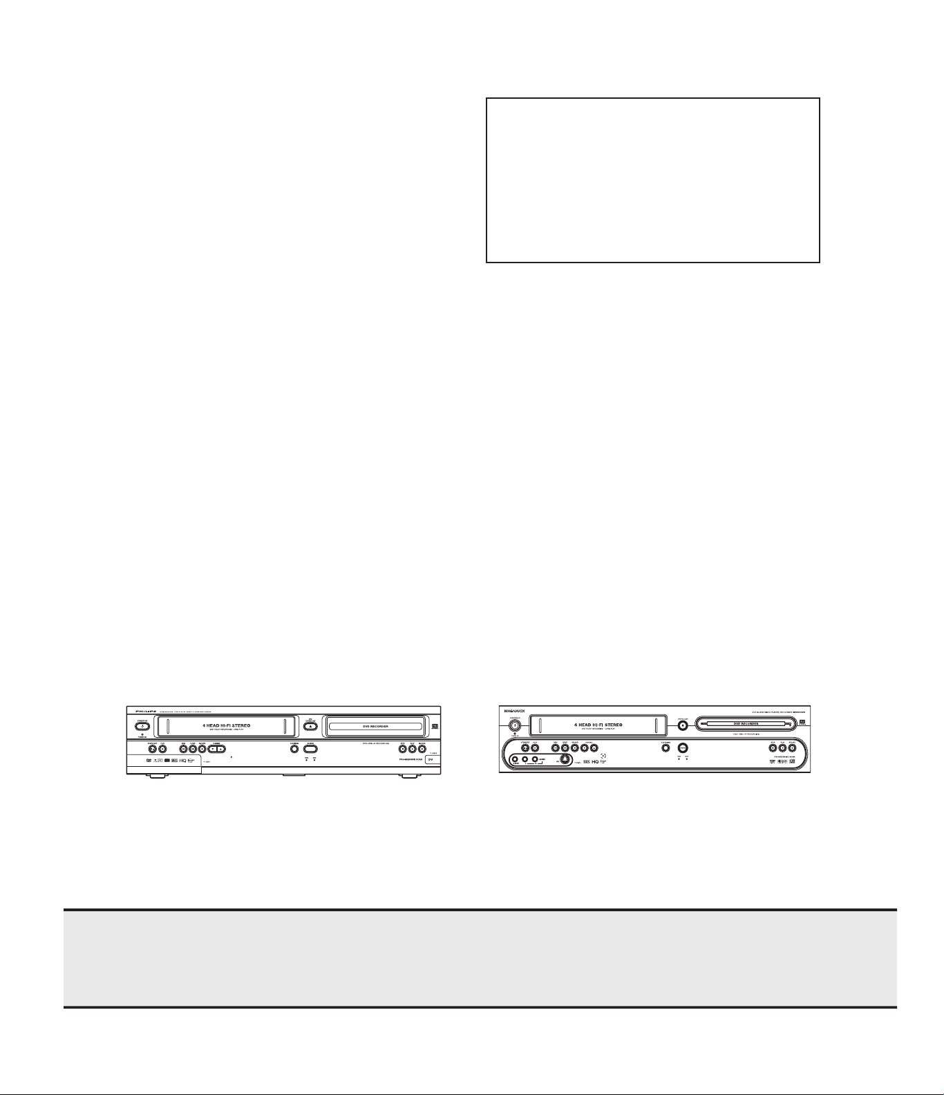
How to Remove / Install Flat Pack-IC
1. Removal
With Hot-Air Flat Pack-IC Desoldering Machine:.
(1) Prepare the hot-air flat pack-IC desoldering
machine, then apply hot air to the Flat Pack-IC
(about 5 to 6 seconds). (Fig. S-1-1)
Pin 1
Instructions for Connectors
1. When you conn ect or disconn ect t he FFC (Flexible
Foil Connector) cable, be sure to first disconnect
the AC cord.
2. FFC (Flexible Foil Connector) cable should be
inserted parallel into the connector, not at an angle.
FFC Cable
Connector
CBA
* Be careful to avoid a short circuit.
Fig. S-1-1
(2) Remove the flat pack-IC with tweezers while apply-
ing the hot air.
(3) Bottom of the flat pack-IC is f ixed with glue to the
CBA; when rem oving enti re flat pa ck-IC, first apply
soldering iron to ce nte r of th e f lat pack-IC a nd hea t
up. Then remove (glue will be melted). (Fig. S-1-6)
(4) Release the flat pack-IC from th e CBA usin g twee-
zers. (Fig. S-1-6)
Caution:
1. T he Flat Pack-IC shape may differ by models. Use
an appropriate hot-air flat pack-IC desoldering
machine, whose shape matches that of the Flat
Pack-IC.
2. D o not supply hot air to the chip par ts around the
flat pack-IC for over 6 seconds because damage to
the chip parts may occur. Put masking tape around
the flat pack-IC to protect other parts from damage.
(Fig. S-1-2)
1-3-1 E6STA
Page 10

3. The fla t pa ck-IC on the CBA is a ffi xed with glue, so
be careful not to break or damage the foil of each
pin or the solder lands under the IC when removing
it.
With Soldering Iron:
(1) Using desoldering braid, remove the solder from all
pins of the flat pack-IC. When you use solder flux
which is applied to all pins of the flat pack-IC, you
can remove it easily. (Fig. S-1-3)
CBA
Masking
Tape
Tweezers
Hot-air
Flat Pack-IC
Desoldering
Machine
Flat Pack-IC
Fig. S-1-2
Flat Pack-IC
Desoldering Braid
Soldering Iron
Fig. S-1-3
(2) Lift each lead of the flat pack-IC upward one by
one, using a shar p pin or wire to which sol der will
not adhere (iron w ire). When h eating the p ins, use
a fine tip soldering iron or a hot air desoldering
machine. (Fig. S-1-4)
Sharp
Pin
Fine Tip
Soldering Iron
(3) Bottom of the flat pack-IC is f ixed with glue to the
CBA; when rem oving enti re flat pa ck-IC, first apply
soldering iron to ce nte r of th e f lat pack-IC a nd hea t
up. Then remove (glue will be melted). (Fig. S-1-6)
(4) Release the flat pack-IC from th e CBA usin g twee-
zers. (Fig. S-1-6)
Fig. S-1-4
1-3-2 E6STA
Page 11
With Iron Wire:
(1)Using desoldering braid, remove the solder from all
pins of the flat pack-IC. When you use solder flux
which is applied to all pins of the flat pack-IC, you
can remove it easily. (Fig. S-1-3)
(2) Affix the wire to a workbench or solid mounting
point, as shown in Fig. S-1-5.
(3) While heating the pins using a fine tip soldering
iron or hot air blower, pull up the wire as the solde r
melts so as to lift the IC leads from the CBA contact
pads as shown in Fig. S-1-5.
(4)B ottom of the flat pack-IC is fixed with glue to the
CBA; when removing entire flat pack-IC, first apply
soldering iron to c en ter o f the fl at pack-IC an d h eat
up. Then remove (glue will be melted). (Fig. S-1-6)
(5)Re lease the fl at pack-IC from the CBA using twee-
zers. (Fig. S-1-6)
Note:
When using a solde ring iron, care must be taken
to ensure that the flat pack-IC is not being he ld by
glue. When the flat pack-IC is removed from the
CBA, handle it gently becau se it may be dama ged
if force is applied.
Hot Air Blower
2. Installation
(1) Using desoldering braid, remove the solder from
the foil of each pin of the flat pack-IC on the CBA so
you can install a replacement flat pack-IC more
easily.
(2) The “I” mark on the flat pack-IC indicates pin 1.
(See Fig. S-1-7.) Be sure this mar k matches the 1
on the PCB when positioning for installation. Then
presolder the four cor ners of the fl at pack-IC. (See
Fig. S-1-8.)
(3) Solder all pins of the flat pack-IC. Be sure that none
of the pins have solder bridges.
Example :
Pin 1 of the Flat Pack-IC
is indicated by a " " mark.
Fig. S-1-7
To Solid
Mounting Point
CBA
Tweezers
Iron Wire
Soldering Iron
Fig. S-1-5
Fine Tip
Soldering Iron
Flat Pack-IC
or
Presolder
Flat Pack-IC
CBA
Fig. S-1-8
Fig. S-1-6
1-3-3 E6STA
Page 12
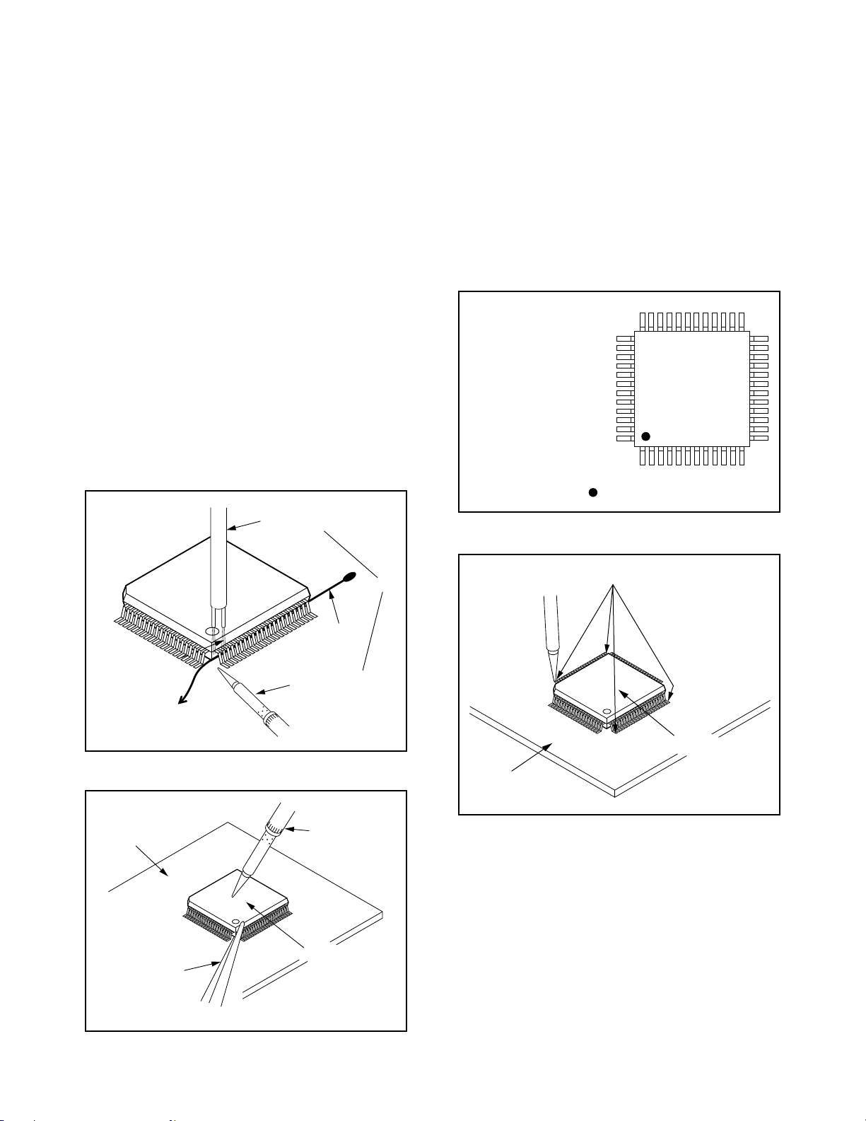
Instructions for Handling
Semi-conductors
Electrostatic breakdown of the semi-conductors may
occur due to a potential dif ference caused by electrostatic charge during unpacking or repair work.
1. Ground for Human Body
Be sure to wear a grounding band (1M Ω) that is prop erly grounded to rem ove any static electr icity that may
be charged on the body.
2. Ground for Workbench
(1)Be sure to place a conductive sheet or copper plate
with proper grounding (1MΩ) on the workbench or
other surface, where the semi-conductors are to be
placed. Because the static electricity charge on
clothing will not escape thr ough the body grounding band, be careful to avoid contacting semi -conductors with your clothing.
<Incorrect>
<Correct>
1MΩ
CBA
Grounding Band
1MΩ
CBA
Conductive Sheet or
Copper Plate
1-3-4 E6STA
Page 13

FUNCTION INDICATOR SYMBOLS
< VCR Section >
Note:
If a mechanical malfunction oc curs, the power is tur ned off. When the power comes on again after that by
pressing [STANDBY-ON] button, an error message is displayed on the TV screen for 5 seconds.
Led Mode Indicator Active
When reel or capstan mechanism is not functioning
correctly
When tape loading mechanism is not functioning
correctly
When cassette loading mechanism is not functioning
correctly
When the drum is not working properly
P-ON+5V Power safety detection
TV screen
“A R” is displayed on a TV screen. (Refer to Fig. 1.)
“A T” is displayed on a TV scr een. (Refer to Fig. 2.)
“A C” is displayed on a TV screen. (Refer to Fig. 3.)
“A D” is displayed on a TV screen. (Refer to Fig. 4.)
“A P” is displayed on a TV screen. (Refer to Fig. 5.)
When reel or capstan mechanism is not functioning
correctly
A
R
Fig. 1
When tape loading me chanism is not func tioning correctly
A
T
Fig. 2
When cassette loadi ng mechanism is not functioning
correctly
When the drum is not working properly
A
D
P-ON+5V Power safety detection
A
P
Fig. 4
Fig. 5
A
C
Fig. 3
1-4-1 E9480FIS
Page 14

< DVD Section >
Note: If an error occurs, a message with the error number appears on the screen.
X X Y Y Z Z
Error code
Nucleus nmber
Nucleus group nmber
Description Error No. Error Description
Sends the device id and the module ids and revisions
of the Domino IC to the stdout port.
Generates a test-image of a selected video standard
on selected video output on the digital board. When no
input is given, the default values will be used. Use
nucleus DS_ANAB_VideoRouting to route the video
signal on the analogue board output.
Switches the test-image off. 010200 Stopping the test image generation succeeded.
Generate an audio sine signal on the audio output of
the digital board.
Stop generating the audio sine signal.
Generate an audio sine signal on the audio output of
the digital board for 4 seconds.
Mute the audio outputs of the digital board. 010600 Muting the audio succeeded.
De-mute the audio outputs of the digital board. 010700 De-muting the audio succeeded.
Check the connection to the DV-LED on the digital
board by switching it on.
Switch off the DV-LED on the digital board. 010900 Switching the DV-LED off succeeded
Peek a value on a specified address.
Poke a value on a specified address.
Check the communication between the IIC controller of
the Chrysalis and the EEPROM.
Check whether the EEPROM can be written to and
read from.
Make the EEPROM empty, containing all zeroes.
Modifies one or more locations in NVRAM and updates
the checksum of the section modified.
010000 Getting the information succeeded.
010100 Generating the test image succeeded.
010101 Failed to set up DENC.
010102 Invalid user input.
010103 Test image not supported.
010300 The sine signal was successfully generated.
010301 Generating the sine test audio failed.
010400 Switching off the audio sine signal succeeded.
010401 Failed to stop sine test audio.
010500 The sine signal burst was successfully generated.
010501 Generating the sine burst f ailed.
010502 Failed to stop the sine burst.
010800 Switching the DV-LED on succeeded.
011200 Peeking on the specified address succeeded.
011201 No address input.
011202 Invalid address.
011300 Poking the specified address succeeded.
011301 No address input.
011302 Invalid address/data.
030000 Something is properly read so the communication is OK.
030004 The communication with the NVRAM failed.
030005 The IIC bus initialisation failed.
030100 The write-read test succeeded.
030101 The IIC bus initialisation failed.
030102 The communication with the NVRAM failed.
030103 The read back value is different from the written value.
030200 The clearing of the NVRAM succeeded.
030201 There was an IIC error .
030202 Clearing the NVRAM failed.
030300 Modifying the NVRAM contents succeeded.
030301 Unable to initialise NVM.
030302 Modifying the NVRAM contents failed.
030303 Length out of range.
030304 Unable to decode length.
030305 Offset out of range.
030306 unable to decode offset.
030307 Unknown location specified.
030308 No location is specified.
030309 Number of values incorrect.
030310 Error creating checksum.
030311 Invalid data.
1-4-2 E9480FIS
Page 15

Description Error No. Error Description
Read out one or more locations in the NVRAM.
Write to a specific memory address.
Read from a specific memory address.
Get the device (revision) type i nformation of the FLASH
IC. (manufacturer and device ID)
Check whether the FLASH can be written to and read
from.
Read from a specific memory address.
Check the checksum of the application partitions by
recalculating and comparing partition checksums.
Calculate the checksum over all memory addresses.
Used to check entire FLASH contents.
Calculate a checksum over a selected number of
address locations.
Get the device (revision) type information of the VIP IC.
Check the communication between the IIC controller of
the Domino and the VIP IC.
Switch the clock output on.
030400 Value read.
030401 Unable to initialise NVM.
030402 Reading the NVRAM contents failed.
030403 Length out of range.
030404 Unable to decode length.
030405 Offset out of range.
030406 Unable to decode offset.
030407 Unknown location specified.
030408 No location is specified.
040200 Writing to the SDRAM succeeded.
040201 No address input.
040202 No data input.
040203 Address is not dividable by 4.
040204 Invalid data.
040205 Address out of rang e.
040206 Invalid address.
040300 Reading from the SDRAM succeeded.
040301 No address input.
040302 Address is not dividable by 4.
040303 Address out of rang e.
040304 Invalid address.
050000 Getting the informat ion from the FLASH succeeded.
050100 The FLASH write-read test succeeded.
050101 Wrong BALO signature.
050102 Wrong CONS signature.
050103 Invalid CONS base.
050104 Invalid CONS end address.
050105 All bits in the TEST region are filled with 0.
050106 The WriteRead test failed.
050107 The Write Failed.
050200 Reading the FLASH succeeded.
050201 No address input.
050202 Invalid address.
050203 Address is out of range.
050204 Address is not dividable by 2.
050300 The checksum is valid, the test succeeded.
050301 Wrong BSTB signature.
050302 Wrong BSTB checksum.
050303 Wrong BALO signature.
050304 Wrong BALO checksum.
050305 Wrong CONS signature.
050306 Wrong CONS checksum.
050307 Invalid BALO end address.
050308 Invalid CONS base.
050309 Invalid CONS end address.
050400 Calculating the checksum over all addresses succeeded.
050500 Calculating the checksum over selected addresses succeeded.
060000 Getting the informa tion from the VIP succeeded.
060001 The IIC bus initialisation failed.
060002 The communication with the VIP failed.
060100 Communicating with the VIP succeeded.
060001 The IIC bus initialisation failed.
060002 The communication with the VIP failed.
060200 Switching the clock output on succeeded.
060201 Switching the clock output on failed.
1-4-3 E9480FIS
Page 16

Description Error No. Error Description
Switch the clock output off.
Select an input video path to be switched to the
analogue output of the VIP.
Get the device (revision) type in formation of the 1394
Physical layer IC.
Check the accessibility of the 1394 Physical layer IC by
writing to and reading from a specific address.
Route a DV stream containing an audio and video
signal through the physical IC to the Domino. This will
be loopthrough to the video output of Domino.
Check whether a DV node can be detected by the
hardware.
Check the device type of the DENC in use.
Check the communication between the IIC controller of
the Domino and the DENC-IC.
Generate a test image and make it present on the
DENC-IC.
Switch off the generated test image.
Turn on MacroVision.
Turn off MacroVision.
Check the communication between the digital board
and the recorder drive by issuing an Inquiry command
over ATAPI bus.
Reset the basic engine.
Return the self-test results through the service port. 090200 Self test succeeded, no errors.
Get the version of the basic engine and that of the
optical unit.
Open the tray of the basic engine.
Close the tray of the basic engine.
060300 Switching the clock output off succeeded.
060301 Switching the clock output off failed.
060400 Selecting the input of the VIP succeeded.
060401 The user provided wrong input.
060402 The VIP was not accessible.
060405 This mode not available on SAA7118.
070100 Getting the informat ion from the physical layer IC succeeded.
070101 Missing PHY clock.
070102 Time-out error.
070103 1394 chip is not IEEE 1394a-2000 compliant.
070300 Communicating with the physical lay er IC succeeded.
070301 Missing PHY clock.
070302 Time-out error.
070303 Register write test failed.
070400 Routing the signals succeeded.
070405 Failed to initialise DENC.
070500 The node was detected OK.
070504 No node was detected.
080100 Communicating with the progressive scan DENC-IC succeeded.
080101 The IIC bus initialisation failed.
080102 No valid DENC detected.
080100 Communicating with the progressive scan DENC-IC succeeded.
080104 Communicating with the DENC failed.
080105 The IIC bus initialisation failed.
080200 The generation of the test image succeeded.
080201 The IIC bus initialisation failed.
080202 Unable to initialise the DENC.
080203 The generation of the test image failed.
080300 Turning off the test image succeeded.
080301 The IIC bus initialisation failed.
080302 The test image could not be tur ned off.
081000 Turning on MacroVision succeeded.
081001 The IIC bus initialisation failed.
081002 Unable to access DE NC.
081000 Turning off MacroVision succeeded.
081001 The IIC bus initialisation failed.
081002 Unable to access DE NC.
090000 Communicating with recorder drive succeeded.
090001 Recorder drive init fails.
090002 Recorder drive command fails.
090100 Resetting the Basic Engine s ucceeded.
090101 Recorder drive init fails.
090300 BE version OK.
090301 Recorder drive init fails.
090302 Recorder drive command fails.
090400 The command executed successfully.
090401 Recorder drive init fails.
090402 Recorder drive command fails.
090500 The command executed successfully.
090501 Recorder drive init fails.
090502 Recorder drive command fails.
1-4-4 E9480FIS
Page 17

Description Error No. Error Description
Write data to and read data from a DVD+RW disc
through the basic engine for verification of the writing.
Write data to and read data from a DVD+R disc
through the basic engine for verification of the writing.
Retrieve the statistical information from the basic
engine.
Reset the statistical information in the basic engine.
Get the error log from the basic engine.
Reset the error log in the basic engine.
090600 The command executed successfully.
090601 Sanyo drive init fails.
090602 Failed to close tray.
090603 Failed to get disc type.
090604 Not DVD+RW disc.
090605 Buffer wait failed.
090606 Write command failed. Sensekey = XX,YY,ZZ.
090607 Failed to synchronize cache. Sensekey = XX,YY,ZZ.
090608 Read command failed. Sensekey = XX,YY,ZZ.
090609 Data read back is different from written data.
090700 The command executed successfully.
090701 Sanyo drive init fails.
090702 Failed to close tray.
090703 Failed to get disc type.
090704 Not DVD+R disc.
090705 Buffer wait failed.
090706 Write command failed. Sensekey = XX,YY,ZZ.
090707 Failed to synchronize cache. Sensekey = XX,YY,ZZ.
090708 Read command failed. Sensekey = XX,YY,ZZ.
090709 Data read back is different from written data.
090710 Failed to read back NWA.
090711 Disc full, insert new DVD+R.
090800 The command executed successfully.
090801 There was a time-out while communicating.
090802 The Basic Engine returned an unexpected result.
090803 The BE returned an error code.
090804 No acknowledge received from BE.
090805 Communicating with the Basic Engine failed.
090806 The BE returned no info.
090900 The command executed successfully.
090901 There was a time-out while communicating.
090902 The Basic Engine returned an unexpected result.
090903 The BE returned an error code.
090904 No acknowledge received from BE.
090905 Communicating with the Basic Engine failed.
091000 The command executed successfully.
091001 There was a time-out while communicating.
091002 The Basic Engine returned an unexpected result.
091003 The BE returned an error code.
091004 No acknowledge received from BE.
091005 Communicating with the Basic Engine failed.
091006 The BE returned no info.
091100 The command executed successfully.
091101 There was a time-out while communicating.
091102 The Basic Engine returned an unexpected result.
091103 The BE returned an error code.
091104 No acknowledge received from BE.
091105 Communicating with the Basic Engine failed.
1-4-5 E9480FIS
Page 18

Description Error No. Error Description
This test measures the average jitter and b ler v alues. A
formatted DVD must be loaded into the engine before
executing this nucleus.
Check whether there is a disc inside the BE.
Read the TOC from the disc. This gives a good
indication if the BE works properly.
Enables Automatic Pattern Verification tool on
DVD+RW disc. Start, stop and type of pattern to be
used can be configured by the user. Return pass/fail
result.
Enables Automatic Pattern Verification tool on DVD+R
disc. Start, stop and type of pattern to be used can be
configured by the user. Return pass/fail result. Note
that the nucleus does not check that the write address
is the correct next available address according to the
DVD+R disc. This must be taken care of by the user,
otherwise the write command will fail.
Set the region code in the AV3.
091200 Optimising jitter succeeded.
091201 There was a time-out while communicating.
091202 The Basic Engine returned an unexpected result.
091203 The Basic Engine returned an error code.
091204 No acknowledge received from BE.
091205 Unable to send tray in.
091206 Unable to read the disc.
091207 No disc is loaded.
091208 Unknown disc is loade d.
091209 Unabl e to enter service mode.
092100 There was a disc inside the set.
092101 Unable to load the tray.
092102 Error received fr om BE .
092400 A disc is loaded, TOC info if echoed.
092401 Unable to load the tray.
092402 The BE has not returned TOC info.
092403 Error received fr om BE .
092600 The command executed successfully.
092601 Not enough in put parameters.
092602 Invalid start address.
092603 Invalid End address.
092604 Invalid pattern.
092605 Sanyo drive init fails.
092606 Failed to close tray.
092607 Failed to get disc type.
092608 Not DVD+RW disc.
092609 Buffer wait failed.
092610 Write command failed. Sensekey = XX,YY,ZZ.
092611 Failed to synchronize chase. Sensekey = XX,YY,ZZ.
092612 Read command failed. Sensekey = XX,YY,ZZ.
092613 Data read back is different from written data.
092700 The command executed successfully.
092701 Not enough in put parameters.
092702 Invalid start address.
092703 Invalid End address.
092704 Invalid pattern.
092705 Sanyo drive init fails.
092706 Failed to close tray.
092707 Failed to get disc type.
092708 Not DVD+R disc.
092709 Buffer wait failed.
092710 Write command failed. Sensekey = XX,YY,ZZ.
092711 Failed to synchronize chase. Sensekey = XX,YY,ZZ.
092712 Read command failed. Sensekey = XX,YY,ZZ.
092713 Data read back is different from written data.
092800 The command executed successfully.
092801 There was a time-out while communicating.
092802 The Basic Engine returned an unexpected result.
092803 The BE returned an error code.
092804 No acknowledge received from BE.
092805 Communicating with the Basic Engine failed.
092806 The user provided wrong input.
1-4-6 E9480FIS
Page 19

Description Error No. Error Description
Read the region code from the AV3.
Reset the region counter in the AV3.
Adjust the DVD-M (with the OPU) with PCBA. (So
adjusts the two PCBS to each other)
Check the communication between the digital board
and the DCB by issuing an echo command.
Get the version of the DCB
Light the entire display of the DCB, and clear the
display after confirmation.User confirmation is
necessary.The REC and PLAY keys on the local
keyboard are used for this confirmation.The PLAY key
confirms that the test pattern is OK and the REC key
indicates an error. The STOP key is used to exit this
nucleus at any time. The keyboard can also be used for
the same purpose. The O or o key confirms that the
test pattern is OK and the N or n key indicates the user
wants to go to the next test or that there is an error . The
rest of the keys of the keyboard are used to exit this
nucleus at any time.
Check all keys of the keyboard by confirming the keycode displayed of each key. The PLAY key is used to
confirm this nucleus. However, this key is also part of
the keyboard test itself. Also the REC and STOP keys
are used to exit the test.With the REC key the user
signals a failure, while the STOP key signals the
abortion of the test by the user. To use one of these
three keys for confirmation,failur e or abortion, the user
needs to hold the key pressed down for more than one
second. Pressing the keyboard will also stop the test at
any time.
092900 The command executed successfully.
092901 There was a time-out while communicating.
092902 The Basic Engine returned an unexpected result.
092903 The BE returned an error code.
092904 No acknowledge received from BE.
092905 Communicating with the Basic Engine failed.
093000 The command executed successfully.
093001 There was a time-out while communicating.
093002 The Basic Engine returned an unexpected result.
093003 The BE returned an error code.
093004 No acknowledge received from BE.
093005 Communicating with the Basic Engine failed.
093100 The command executed successfully.
093101 There was a time-out while communicating.
093102 The Basic Engine returned an unexpected result.
093103 The BE returned an error code.
093104 No acknowledge received from BE.
093105 Communicating with the Basic Engine failed.
093106 Unabl e to enter service mode.
093107 This nucleus is not supported by the engine.
100000 Communicating with the DCB succeeded.
100001 DCB could not be ac cess ed by the analogue board.
100002 There was no response from the analogue board.
100003 The error code returned from the analogue board is unknown.
100004 There was no response from the front panel.
100100 Retrie ving the v ersion of the DCB succeeded.
100101 DCB could not be ac cess ed by the analogue board.
100102 There was no response from the analogue board.
100103 The error code returned from the analogue board is unknown.
100200 Lighting the entire display succeeded.
100201 DCB could not be ac cess ed by the analogue board.
100202 There was no response from the analogue board.
100203 The error code returned from the analogue board is unknown.
100206 The DCB did not light all labels.
100207 The user skipped the rest of the test.
100208 The user returned an unknown confirmation.
100400 All the keys on the keyboard have been pressed.
100401 DCB could not be ac cess ed by the analogue board.
100402 There was no response from the analogue board.
100403 The error code returned from the analogue board is unknown.
100404 Not all the keys w ere pressed.
100405 In valid key code returned.
100406 DCB Keyboard; test failed.
100407 DCB Keyboard; test aborted.
100408 Failed to clear FP buffer.
100409 Test stopped from service port.
1-4-7 E9480FIS
Page 20
Description Error No. Error Description
Check the interface between the remote control and
the DCB by checking the key-code displayed. At least
one key must be tested. The test can be exited by
pressing the STOP-,REC-, or PLAY-key on the local
keyboard. The user should press PLAY to indicate a
successful test. The REC-key is pressed if the test
failed, and ST OP can be pressed to abort the test. The
keyboard can also be used for the same pur pose .The
O or o key stops the test and the N or n key indicates
an error. The rest of the keys of the keyboard are used
to abort this test at any time.
Switch the record LED on, and after confirmation off.
The user confirms by pressing the REC key, ST OP ke y,
or the PLAY key on the local keyboard. The PLAY key
confirms that the LED is on and the REC key indicates
an error. The STOP key signals the abortion of the test
by the user. The keyboard can also be used for the
same purpose . The O or o key confirms that the test
pattern is OK and the N or n key indicates an error or
that the user wants to go to the next test. The rest of
the keys of the ke yboard are used to e xit this n ucleus at
any time. After that the nucleus switches the LED off.
Check the communication between the digital board
and the analogue board by issuing some echo string.
Check the communication between the digital board
and the NVRAM on the analogue board.
Check the communication between the digital board
and the tuner on the analogue board.
Check the communication between the digital board
and the data slicer on the analogue board.
Check the communication between the digital board
and the sound processor on the analogue board.
Check the communication between the digital board
and the A/V-selector on the analogue board.
Get the hardware version of the analogue board.
Get the software version of the boot software of the
analogue board.
100500 Remote Control test succeeded.
100501 DCB could not be ac cess ed by the analogue board.
100502 There was no response from the analogue board.
100503 The error code returned from the analogue board is unknown.
100504 DCB Remote control; no user input received.
100505 DCB Remote control; test failed.
100506 DCB Remote control; test aborted.
100507 Failed to clear FP buffer.
100508 Test stopped from service port.
100600 Switching Led on succeeded.
100601 DCB could not be ac cess ed by the analogue board.
100602 There was no response from the analogue board.
100603 The DCB did not light all the leds.
100604 The user skipped the rest of the test.
100605 The user returned an unknown confirmation:
100606 The error code returned from the analogue board is unknown.
110000 Communicating with the analogue board succeeded.
110001 The test returned the wrong string.
110002 Communicating with the analogue board failed.
110103 The analogue board returned an unexpected result.
110104 Receiving character failed.
110100 Communicating with the NVRAM on the analogue board succeeded.
110101 The analogue board could not communicate with the NVRAM.
110102 Communicating with the analogue board failed.
110103 The analogue board returned an unexpected result.
110104 The write-read test failed.
110200 Communicating with the tuner on the analogue board succeeded.
110201 The analogue board could not communicate with the tuner.
110202 Communicating with the analogue board failed.
110203 The analogue board returned an unexpected result.
110300
110301 The analogue board could not communicate with the data slicer.
110302 Communicating with the analogue board failed.
110303 The analogue board returned an unexpected result.
110400
110401
110402 Communicating with the analogue board failed.
110403 The analogue board returned an unexpected result.
110500
110501 The analogue board could not communicate with the A/V selector.
110502 Communicating with the analogue board failed.
110503 The analogue board returned an unexpected result.
110600 Reading the hardware version succeeded.
110601 The segment containing the hardware version could not be found.
110602 Communicating with the analogue board failed.
110603 The analogue board returned an unexpected result.
110700 Reading the boot-software version succeeded.
110701 The segment containing the boot-software v ersion could not be f ound.
110702 Communicating with the analogue board failed.
110703 The analogue board returned an unexpected result.
Communicating with the data slicer on the analogue board
succeeded.
Communicating with the sound procesor on the analogue board
succeeded.
The analogue board could not communicate with the sound
processor.
Communicating with the A/V selector on the analogue board
succeeded.
1-4-8 E9480FIS
Page 21

Description Error No. Error Description
Get the software version of the download software of
the analogue board.
Get the software version of the application software of
the analogue board.
Get the software version of the diagnostic software of
the analogue board.
Check the checksum of the several part itions by
recalculating and comparing partition checksums.
Perform the routing of the video paths on the analogue
board.
Perform the routing of the audio paths on the analogue
board.
Set the tuner to receive a valid audio and video signal
Perform an IIC write and read action on the analogue
board
Set the clock to the value passed through in the YYYY
MM DD HH MM SS format.
Generate a 1 kHz signal on pin 7 (INT) of the clock IC.
Store the clock IC correction value in NVRAM.
110800 Reading the download-software version succeeded.
110801
110802 Communicating with the analogue board failed.
110803 The analogue board returned an unexpected result.
110900 Reading the application-software version succeeded.
110901
110902 Communicating with the analogue board failed.
110903 The analogue board returned an unexpected result.
111000 Reading the diagnostics-software version succeeded.
111001
111002 Communicating with the analogue board failed.
111003 The analogue board returned an unexpected result.
111100 Checksum calculation succeeded.
111101
111102 Communicating with the analogue board failed.
111103 Communicating with the analogue board failed.
111104 The analogue board returned an unexpected result.
111200 Routing the video on the analogue board succeeded.
111201 Routing the video on the analogue board failed.
111202 The user provided wrong input.
111203 Communicating with the analogue board failed.
111204 The analogue board returned an unexpected result.
111300 Routing the audio on the analogue board succeeded.
111301 Routing the audio on the analogue board failed.
111302 The user provided wrong input.
111303 Communicating with the analogue board failed.
111304 The analogue board returned an unexpected result.
111400 Setting the tuner ch annel succeeded.
111401 Setting the tuner channel failed.
111402 The user provided wrong input.
111403 Communicating with the analogue board failed.
111404 The analogue board returned an unexpected result.
111500 Reading and writing IIC on the analogue board succeeded.
111501 Reading or writing IIC on the analogue board failed.
111502 The user provided wrong input.
111503 Communicating with the analogue board failed.
111504 The analogue board returned an unexpected result.
111600 Adjusting the clock succeeded.
111601 Adjusting the clock failed.
111602 The user provided wrong input.
111603 Communicating with the analogue board failed.
111604 The analogue board returned an unexpected result.
111700 Generating the signal on the designated pin succeeded.
111701 Generating the signal on the designated pin failed.
111702 Communicating with the analogue board failed.
111703 The analogue board returned an unexpected result.
111800 Storing the correction value for the clock in NVRAM succeeded.
111801 Storing the correction value for the clock in NVRAM failed.
111802 Invalid input; default value stored.
111803 Communicating with the analogue board failed.
111804 The analogue board returned an unexpected result.
111805 The user provided wrong input.
The segment containing the download-software version could not be
found.
The segment containing the application-software version could not be
found.
The segment containing the diagnostics-software version could not be
found.
Either the segment could not be found or the checksum was not
correct.
1-4-9 E9480FIS
Page 22
Description Error No. Error Description
111900 Storing the reference voltage f or the tuner in NVRAM succeeded.
111901 Storing the reference voltage for the tuner in NVRAM failed.
Store the reference voltage for the tuner in NVRAM.
Store the frequency table in NVRAM. The frequency
table is passed through the error-string provided to the
nucleus.
Store the external presets in NVRAM.
Measure the audio signal corresponding to 0dB per
channel and store it as correction value in NVRAM
Check communication to VCR module via SIO interface
Get the hardware version and type of the digital board. 120000 Getting the hardware version and type of the digital board succeeded.
Get the version of the boot stub software on the digital
board.
Get the version of the download software on the digital
board.
Get the version of the application software on the
digital board.
Upload the contents of the NVRAM on the analogue
board or the digital board to the service PC, by using
the X-modem protocol.
Download a file with the contents of the NVRAM f or the
analogue board or the digital board from the service
PC to the recorder, by using the X-modem protoc ol.
Set the IEEE 1394 unique ID.
Get the IEEE1394 unique ID.
111902 The user provided wrong input.
111903 Communicating with the analogue board failed.
111904 The analogue board returned an unexpected result.
112000 Downloading the frequency table in NVRAM succeeded.
112001 Downloading the frequency table in NVRAM failed.
112002 The user provided wrong input.
112003 Communicating with the analogue board failed.
112004 The analogue board returned an unexpected result.
112100 Storing the external presets in NVRAM succeeded.
112101 Storing the exter nal preset s in NVRAM failed.
112102 Communicating with the analogue board failed.
112103 The analogue board returned an unexpected result.
112200 Storing the bargraph adjustment values in NVRAM succeeded.
112201 Storing the bargraph adjustment values in NVRAM failed.
112202 Communicating with the analogue board failed.
112203 The analogue board returned an unexpected result.
112300 Communication to VCR succeeded.
112201 Communicating with the analogue board failed..
112302 Wrong SIO CRC received.
112303 No SIO data received.
112304 The analogue board returned an unexpected result.
120100 Getting the Boot software version succeeded.
120200 Getting the Download software version succeeded.
120300 Getting the Application software version succeeded.
120301 Invalid CONS base address.
120500 Download succeeded.
120501 User input is n ot valid.
120502
120503 Something went wrong while transferring the data.
120504 User cancelled the upload.
120600 Download succeeded.
120601 The write to NVRAM failed.
120602 Timeout. Too many retries.
120603 A file was sent with a wrong header.
120604 User cancelled the download.
120605 User input is n ot valid.
120606 Unknown Error.
120700 Setting the unique DV ID succeeded.
120701 User input is n ot valid.
120702 Setting the unique DV ID failed.
120703 Write succeeded, but checksum is corr upt .
120704 Error initialising I2C.
120800 Getting the unique DV ID succeeded.
120801 Getting the unique DV ID failed.
Something went wrong while copying the data from NVRAM to
SDRAM .
1-4-10 E9480FIS
Page 23

Description Error No. Error Description
120900 Writing the data over IIC succeeded.
120901 No input specified.
120902 In valid Bus ID number.
120903 No IIC address.
120904 Invalid IIC address.
120905 No number of bytes input.
Perform an IIC write action on the digital board.
Perfo r m an IIC read action on the digital board.
Perform an UART write action on the digital board on a
specified UART.
Perfo r m an UART read action on the digital board on a
specified UART
The video signal, which is determined by the user
input, is routed from the input to the output. Input is set
with the routing nucleus 1112. All outputs are enabled.
Audio loopthrough is also enabled by this nucleus.
Stop routing the audio/video input to all the outputs.. 121400 VideoLoopthroughStop succeeded.
Set the slash version of the system.
Get the slash version of the system.
(Re-) Virginize the recorder. User data in the NVRAM
of the analogue board is cleared.
Turn on the virgin mode functionality (e.g. the auto
channel search upon startup).
120906 Invalid number of bytes.
120907 No Data.
120908 Number of bytes must be > 0 and < 18.
120909 Invalid Data.
120910 Not enough data bytes.
120911 IIC Write fail ed.
120912 IIC init f ailed.
121000 Reading the data ov er IIC succeeded.
121001 No input specified.
121002 In valid Bus ID number.
121003 No IIC address.
121004 Invalid IIC address.
121005 No number of bytes input.
121006 Invalid number of bytes.
121007 Number of bytes must be > 0 and < 101.
121008 IIC Read failed.
121009 IIC init f ailed.
121100 Writing the bytes to the UART succeeded.
121101 The user provided wrong input.
121102 Writing to the UART failed.
121200 Reading the data from the UAR T succeeded.
121201 The user provided wrong input.
121202 Reading the data from the UAR T failed.
121300 Video LoopthroughStart succeeded.
121302 Invalid input parameters.
121303 Failed to initialise DENC.
121304 Failed to initialise VIP.
121305 DSW not ready for this setting yet.
121700 Setting the slash version succeeded.
121701 Invalid slash version, default version is set.
121702 Setting the slash version failed.
121703 The user provided wrong input.
121705 No DS errCode known for analogue board error:
121706 There was no response from the analogue board.
121800 Getting the slash version succeeded.
121801 Getting the slash version f ailed.
121802 The IIC write failed.
121803 The IIC read failed.
121804 There was no response from the analogue board.
121805 No DS errCode known for analogue board error:
121900 Virginization succeeded.
121901 Virginization on the Analogue Board failed.
121903 No DS errCode known for analogue board error:
121904 There was no response from the analogue board.
122000 Turning on the virgin mode succeeded.
122001 urning on VirginMode on the Analogue Board failed.
122003 No DS errCode known for analogue board error:
122004 There was no response from the analogue board.
1-4-11 E9480FIS
Page 24

Description Error No. Error Description
Turn off the virgin mode functionality (e.g. the auto
channel search upon startup).
122100 Turning off the virgin mode succeeded.
122101 Turning off VirginMode on the Analogue Board failed.
122103 No DS errCode known for analogue board error:
122104 There was no response from the analogue board.
1-4-12 E9480FIS
Page 25

PREPARATION FOR SERVICING
How to Enter the Service Mode
About Optical Sensors
Caution:
An optical sensor system is used for the Tape Start
and End Sensors on this equipment. Carefully read
and follow the instructions below. Otherwise the unit
may operate erratically.
What to do for preparation
Insert a tap e into the Deck Mechan ism Assembly and
press the PLAY button. The tape will be loaded into
the Deck Mechanism Assembly. Make sure the power
is on, connect TP204 (S-INH) to GND. This will stop
the function of Tape Start Sensor, Tape End Sensor
and Reel Sensors. (If these TPs are c onne ct ed before
plugging in the unit, the function of the sensors will
stay valid.) See Fig. 1.
Q236
Q238
TP204
S-INH
Fig. 1
Note: Because the Tape End Se nsors are in active, do
not run a tape all the way to the start or the en d of the
tape to avoid tape damage.
1-5-1 E9480PFS
Page 26

OPERATING CONTROLS AND FUN CTIONS
[ DVDR600 VR/37 ]
1-6-1 E9480IB
Page 27

1-6-2 E9480IB
Page 28
1-6-3 E9480IB
Page 29

[ MRV700VR/17 ]
1-6-4 E9480IB
Page 30
1-6-5 E9480IB
Page 31

1-6-6 E9480IB
Page 32

[ DVDR600 VR/37 ]
REMOTE CONTROL OPERATION
1-7-1 E9480IBR
Page 33

1-7-2 E9480IBR
Page 34

[ MRV700VR/17 ]
1-7-3 E9480IBR
Page 35

1-7-4 E9480IBR
Page 36

CABINET DISASSEMBLY INSTRUCTIONS
Comparison Chart of Models and Marks
Model Mark
DVDR600VR/37 A
MRV700VR/17 B
1. Disassembly Flowchart
This flowchar t indicates the disassembly steps to gain
access to item(s ) to be ser v iced. When reasse mbling,
follow the steps in reverse order. Bend, route, and
dress the cables as they were originally.
[9] FFC
Friction Plate
[10] Rear
Panel Unit
[11] Power
Supply CBA
[13] PCB
Holder
[14] Rear
Panel
[17] VCR
Chassis Unit
[20] Main
CBA
[21] CPU
CBA Unit
[1] T op Cover
[2] Front
Assembly
[5] Jack-A
CBA
[6] Jack-B
CBA
[12] DC
Fan Motor
[23] Front
Bracket R
[22] Deck
Pedestal
[18] Deck
Assembly
[19] Function
CBA
[3] Front
Bracket
[4] Radiation
Sheet
[7] DVD Mecha
& FE Assembly
[8] Digital Board
Unit
[15] Front CBA
[16] Bracket R
2. Disassembly Method
ID/
LOC.
No.
PART
Fig.
No.
[1] Top Cover D1 6(S-1) ---
Front
[2]
[3]
[4]
[5]
[6]
Assembly
Front
Bracket
Radiation
Sheet
Jack-A
CBA
Jack-B
CBA
D2
D2 2(S-2), 2(S-3) ---
D2 ---------- ---
D3 3(S-5) ---
D3 2(S-6) ---
DVD
Mecha &
FE
D4
[7]
Assembly
Digital
[8]
Board
D4
Unit
FFC
[9]
Friction
D5 2(S-10) ---
Plate
Rear
[10]
Panel Unit
D5
Power
[11]
Supply
D6
CBA
DC Fan
[12]
[13]
[14]
Motor
PCB
Holder
Rear
Panel
D6 2(S-15) ---
D6 3(S-16) ---
D6 ---------- ---
[15] Front CBA D7 3(S-17), *CN214 --[16] Bracket R D7 2(S-18) ---
VCR
[17]
Chassis
D7
Unit
REMOVAL
REMOVE/*UNHOOK/
UNLOCK/RELEASE/
UNPLUG/DESOLDER
*2(L-1), Tra y Panel,
*5(L-2), *3(L-3),
*CN204, *CN205
2(S-7), 2(S-8),
*CN207, *CN208,
*CN211, *CN213,
Connector 1109,
Connector 1704
4(S-9), Connector
1102
5(S-11), 3(S-12), (S-
13), *CN209, *CN210
4(S-14), AC Cord,
Earth Plate
5(S-19), 5(S-20),
(S-21)
Note
1
1-1
1-2
1-3
1-4
1-5
1-6
1-7
---
---
---
---
---
1-8-1 E9480DC
Page 37

ID/
LOC.
No.
[18]
[19]
PART
Deck
Assembly
Function
CBA
REMOVE/*UNHOOK/
Fig.
UNLOCK/RELEASE/
No.
UNPLUG/DESOLDER
(S-22), (S-23),
D8
Desolder
Note
D8 Desolder ---
2
3
[20] Main CBA D8 ---------- ---
REMOVAL
[21]
[22]
[23]
↓
(1)
CPU CBA
Unit
Deck
Pedestal
Front
Bracket R
↓
(2)
4(S-24), *C N215,
D8
*CN216
---
D9 8(S-25) ---
(S-26), 2(S-27),
D9
iLink Cable [ A ]
↓
(3)
↓
(4)
---
↓
(5)
Note:
(1): Identification (location) No. of parts in the figures
(2): Name of the part
(3):Figure Number for reference
(4): Identification of parts to be removed, unhooked,
unlocked, released, unplugged, unclamped, or
desoldered.
P=Spring, L=Locking Tab, S=Screw ,
CN=Connector
*=Unhook, Unlock, Release, Unplug, or Desolder
e.g. 6(S-1) = six Screws (S-1),
5(L-1) = five Locking Tabs (L-1)
(5):Refer to “Reference Notes.”
Reference Notes
aligning the hole of C am Gear with the pin of LDSW, the sh aft of Cam Gear with the hol e of LD-SW
as shown in F ig. D8.
(S-1)
(S-1)
[1] T op Cover
(S-1)
Fig. D1
(S-2)
[3] Front
[4] Radiation Sheet
(S-2)
(S-3)
Bracket
CN204
CN205
Trya Panel
(L-2)
CAUTION 1: Locking Tabs (L-1), (L-2) and (L-3) are
fragile. Be careful not to break them.
1-1. Connect the wall plu g to an AC outlet and press
the [OPEN/CLOSE] button to open the tray.
1-2. Remove the Tray Panel by releasing two locking
tabs (L-1 ).
1-3. Press the [OPEN/CL OSE] button again to close
the tray.
1-4. Press the [POWER] button to turn the power off.
1-5. Unplug the AC cord.
1-6. Disconnect connectors CN204 and CN205.
1-7. Release five Locking Tabs (L-2). Then release
three Locking Tabs (L-3), and remove the Front
Unit.
2. When re ass em bling, s old er wire j ump er s a s s hown
in Fig. D8.
3. Before installing the Deck Assembly, be sure to
place the pin of LD-SW on M ain CBA as shown in
Fig. D8. Then, install the Deck Assembly while
(L-1)
(L-1)
(L-2)
[2] Front
Assembly
(L-3)
(L-2)
Fig. D2
1-8-2 E9480DC
Page 38

[5] Jack-A CBA
(S-5)
(S-6)
(S-12)
(S-13)
[9] FFC Friction Plate
(S-11)
(S-10)
[7] DVD
Mecha
& FE
Assembly
(S-7)
[6] Jack-B CBA
(S-8)
Fig. D3
(S-12)
CN210
[14] Rear Panel
[10] Rear
Panel Unit
(S-12)
CN209
Fig. D5
Connector 1109
Connector 1704
(S-9)
Connector
1102
CN208
(S-9)
[8] Digital
Board Unit
(S-9)
CN213
CN207
CN211
Fig. D4
AC Cord
Hook
[11] Power
Supply CBA
(S-14)
(S-14)
(S-14)
(S-16)
(S-15)
(S-16)
[12] DC Fan Motor
[13] PCB
Holder
Earth Plate
Fig. D6
1-8-3 E9480DC
Page 39

(S-19)
(S-20)
(S-20)
(S-19)
(S-19)
(S-20)
CN214
(S-20)
(S-21)
[17] VCR
Chassis
Unit
(S-17)
(S-20)
(S-17)
(S-18)
[16]
Bracket R
[15]
Front
CBA
Fig. D7
1-8-4 E9480DC
Page 40

FE Head
CN215
Cylinder
Assembly
ACE Head
Assembly
[18] Deck
Assembly
(S-24)
[21] CPU CBA
Unit
Pin
SW202
LD-SW
(S-24)
CN216
(S-22)
[19] Function
CBA
(S-23)
Desolder
[20] Main
CBA
Lead with
blue stripe
(S-24)
From
ACE Head
Assembly
[20] Main CBA
LD-SW
Lead with
blue stripe
[18] Deck Assembly
Shaft
Hole
From
Cylinder
Assembly
Hole
Pin
From
FE Head
Cam Gear
[20] Main CBA
From
Capstan
Motor
Assembly
Lead with
Printing side
Desolder
blue stripe
Lead with
gray stripe
Desolder
BOTT OM VIEW
Lead connections of Deck Assembly and Main CBA
1-8-5 E9480DC
Desolder
Fig. D8
Page 41

[ A ]
(S-25)
(S-25)
[22] Deck
Pedestal
[23] Front
Bracket R
(S-27)
iLink Cable
(S-26)
Fig. D9
1-8-6 E9480DC
Page 42

HO W TO EJECT MANUALLY
1. Put tape on the Maintenance Tool. (Please use a metallic plate as shown below as a maintenance tool.)
Maintenance T ool
Tape
1
Size
50mm 7mm
0.4mm
R6.5mm
2. Insert the Maintenance Tool under the Tray Panel as shown.
3. Pull out and raise the Maintenance Tool up as shown to release two locking tabs of the Tray Panel.
4. Remove the Tray Panel.
Release3
Tray Panel
4
3
2
Tray Panel
3
Release two Locking Tabs
5.4mm
3
Maintenance T ool
Maintenance T ool
2
Side view
5. Insert the Ejection Pin straightly into the ejection hole to open the tray.
(Recommended size of the Ejection Pin: diameter; 1.2 mm, length; more than 50mm)
5
5
5
Ejection Pin
Ejection Pin
Recommended size:
- Diameter: 1.2 mm
- Length: more than 50 mm
Ejection hole
Side view
1-8-7 E9480DC
Page 43

HOW TO INITIALIZE THE DVD RECORDER
To put the program back at the factory-default, initialize
the DVD recorder using the following procedure.
1. Press and hold the [DVD STOP C] button on the
DVD recorder.
2. Insert the AC plug to an AC outlet.
3. Release [DVD STOP C] button after 5 or 6 seconds.
1-8-8 E9480DC
Page 44

ELECTRICAL ADJUSTMENT INSTRUCTIONS
c
General Note: "CBA" is an abbreviation for
"Circuit Board Assembly."
NOTE:
1.Electric al adjust ments are required a fter repla cing
circuit components and ce rtain mechanical par ts.
It is impor tant to do these adjustments only after
all repairs and replacements have been completed. Also, do not attempt these adjustments
unless the proper equipment is available.
2.To perform thes e alignment / confirmation procedures, make sure that the tracking control is set in
the center position: P ress either " CHANNEL L5??" or
"CHANNEL K" button on th e front panel first , then
the "PLAY" button on the front panel.
CH1
CH2
Figure 1
EXT. Syncronize Trigger Point
1.0H
6.5H±1H (412.7µs±63.5µs)
Switching Pulse
0.5H
V-Syn
Test Equipment Required
1.Oscilloscope: Dual-trace with 10:1 probe,
V-Range: 0.001~50V/Div.,
F-Range: DC~AC-20MHz
2.Alignment Tape (VFMS0001H6)
Head Switching Po sition Adjustment
Purpose:
To determine the Head Switching position dur ing
playback.
Symptom of Mi sadjustm e n t:
May cause Head Switching noise or ver tical jitter
in the picture.
Test point Adj.Point Mode Input
TP751(V-OUT)
TP302(RF-SW)
GND
Tape
VR201
(Switching Point)
(MAIN CBA)
Measurement
Equipment
PLAY
(SP)
Spec.
Reference Notes:
Playback the Alignment tape and adjust VR201 so that
the V-sync front edge of the CH1 video output waveform is at the 6.5H±1H (412.7µs±63.5µs) delayed
position from the risi ng edge of the CH2 head switching pulse waveform.
-----
VFMS0001H6 Oscilloscope
Connections of Measurement Equipment
TP751
Main CBA
GND
TP302
(412.7µs±63.5µs)
Oscilloscope
6.5H±1H
CH1 CH2
Trig. (+)
1-9-1 E9480EA
Page 45

Adjustment Points and Test Points
Main CBA Top View
TP751 V-OUT
TP301 C-PB
TP302 RF-SW
VR201 SW-P
TP513 CTL
TP204 S-INH
TEST POINT INFORMATION
: Indicates a test point with a jumper wire across a hole in the PCB.
TEST POINTS NOT USED IN ELECTRICAL ADJUSTMENTS
Test Point
TP301
TP302
TP513
TP204
Mechanical Alignment Procedures
Mechanical Alignment Procedures
Mechanical Alignment Procedures
Preparation for Servicing
DVD/VCR S-Video In (EXT2)
DVD/VCR S-Video Out
Used in: Page No.
DVD/VCR S-Video In
DVD/VCR Component Video Out
DVD/VCR Video In (EXT2)
DVD/VCR Video Out
2-3-3, 2-3-4
2-3-3, 2-3-4
2-3-3
1-5-1
DVD/VCR Audio R In
DVD/VCR Audio L In
DVD/VCR Video In
DVD/VCR Component Video In (EXT1)
DVD Coaxial Out
DVD/VCR Audio L In (EXT1)
DVD/VCR Audio R In (EXT1)
DVD/VCR Audio L Out
DVD/VCR Audio R Out
Antenna In
Antenna Out
DVD/VCR Audio L Out
DVD/VCR Audio R Out
DVD/VCR Audio L In (EXT2)
DVD/VCR Audio R In (EXT2)
1-9-2 E9480EA
Page 46

FIRMWARE RENEWAL MODE
1. Make a copy of the data for upda te to a CD-R or
CD-RW.
2. Set the disc made in Step 1 on the tray and close.
3. Turn on the DVD recorder while pushing [DVD
OPEN/CLOSE A] button and [DVD RECORD I]
button at the same time. Updat e of F/W will begin
after “FORCED DOWN” is displayed on DVD FLD.
4. Up date of F/W will be performe d automatica lly and
the DVD recorder will be in the standby mode.
Then press [DVD OPEN/CLOSE A] button on the
DVD recorder and remove the disc.
1-10-1 E9480TEST
Page 47

REWORK PROCEDURE IEEE UNIQUE NUMBER
The procedure describ es how to upgrade sets with a
unique number after repair. This unique number is
stored in the NVRAM o f the FEB E board a t the en d of
the production line.
This procedure is only valid or necessary when:
- The FEBE board is replaced
- NVRAM on the FEBE board is replaced
- NVRAM is cleared
In all other cases the repaired set retain s its unique
number.
The procedure defines several means to re-assure the
unique number depending on the possibilities of repair
or the state the faulty set is in.
1. Connect defective digital board to PC via serial
cable.
2. Start up hyper ter minal or any other seria l ter minal
via the correct settings (DSW command mode
interface).
3. Read out existing unique number via 1208.
DS:> 1208
4. Press [ENTER] button on the remote control unit.
120800: The DvIdNumber is:
Test OK @
**********
5. Note read out.
6. Program new digital board via nucleus 1207.
DS:> 1207
**********
7. Press [ENTER] button on the remote control unit.
120700: Test OK @
8. The set has now the original unique number.
1-10-2 E9480TEST
Page 48

BLOCK DIAGRAMS
Servo / System Control Block Diagram
D952 DVD
D951 VCR
FUNCTION CBA
OUTPUT
SW951
CN952CN206
42KEY-2
24VCR LED
51DVD LED
CLOCK
IC218(EEPROM)
6
DATA
5
TO Hi-Fi AUDIO
BLOCK DIAGRAM
Hi-Fi-H-SW
IIC-BUS SCL
IIC-BUS SDA
12
13IIC-BUS SCL
25
Hi-Fi-H-SW
IIC-BUS SDA
NORMAL-L
D751
KEY SWITCH
JACK-A CBA
CN751CN205
22KEY-1
33KEY-1-2
11POWER LED
66
67
KEY- 2
KEY- 1
POWER
KEY SWITCH
JACK-B CBA
CN901CN204
66KEY-1-2
DRIVE
DRIVE
Q245
Q242
73
VCR-IND 70
POWER-IND
KEY SWITCH
55KEY-2
77S-INH
S-INH
TP204
DRIVE
Q243
DVD-IND 71
A-MUTE-H
A-MUTE-H
59
Hi-Fi/NOR-IN
TO AUDIO
BLOCK DIAGRAM
D-REC-H
YCA-SCL
YCA-SDA
24
26
D-REC-H
A-MUTE-H
YCA-CS
YCA-SCL
YCA-SDA
14
15
YCA-SCL
YCA-SDA
YCA-CS
C-SYNC
41
16
YCA-CS
C-SYNC
D-V SYNC
TO VIDEO
BLOCK DIAGRAM
V-ENV
RF-SW
H-A-SW
C-ROTA
79
18
786419
V-ENV
RF-SW
H-A-SW
C-ROTA
D-V SYNC
TO SUB SYSTEM CONTROL
BLOCK DIAGRAM
CS
SDAI
SDAO
H-A-COMP
7
8
1
80
CS
SDAI
SDAO
H-A-COMP
SCLK
6
SCLK
DISPLAY-CLK
DISPLAY-DATA
IC228
(SERVO/SYSTEM CONTROL)
10
11
MAIN CBA
DIN
CLK
~
7G
1G
IC221
(FIP DRIVER)
IC225
~
23
17
GRIDFIP
:INDICATES A TEST POINT WITH A JUMPER WIRE ACROSS A HOLE IN THE PCB.
:USED TO INDICATE A TEST POINT WITH A COMPONENT LEAD ON FOIL SIDE.
:USED TO INDICATE A TEST POINT WITH NO TEST PIN.
:USED TO INDICATE A TEST POINT WITH A TEST PIN.
TEST POINT INFORMATION
" " = SMD
DISPLAY-ENA
9
RM201
2281
STB
~
h
a
~
7
14
SEGMENT
SENSOR
REMOTE
REMOTE-DVD
TO SUB SYSTEM
i
16
AL+5V
REMOTE-VIDEO
CTL(+)
CTL58CTL(-)
5
56
CTL
TP513
CONTROL BLOCK
DIAGRAM
D229
S-LED
CL504
CN203
5 CTL(+)
57
6 CTL(-)
AL+5V
SW202
LD-SW
TP507
TP506 TP205
LD-SW68
END-S
T-REEL
ST-S
Q238
ST-S
T-REEL
END-S
3
69
62
ST-S
SENSOR CBA
Q240
Q231,Q235
T-REEL
Q236
RESET
20
RESET
AL+5V
AL+5V
VR201
END-S
SENSOR CBA
PG-DELAY
65
SW-POINT
REC-
2
AL+5V
C-FG
C-F/R
49
27
REC SW
P-ON+5V
AL+12V(1)
C-F/R5C-CONT6GND7LM-FWD/REV
1 AL+12V(1)
2 P-ON+5V
3 C-FG
4
C-CONT
28
SAF-SW
SW201
CN202
M
CAPSTAN MOTOR
CAPSTAN
MOTOR
LM-FWD/REV
D-CONT29
D-PFG
47
21
D-CONT9D-PFG10GND11AL+12V(1)
8
M
P-ON-L
AL+18V
TO POWER SUPPLY
AL+18V
12
P-ON-L
22
BLOCK DIAGRAM
AC HEAD ASSEMBLY
CONTROL
HEAD
(DECK ASSEMBLY)
1-11-1
SENSOR
M
DRUM
MOTOR
PG
CYLINDER ASSEMBLY
LOADING
MOTOR
E9480BLS
Page 49

Sub System Control Block Diagram
FIP801
FUNCTION CBA
OPEN/CLOSE
DUBBING
SW203
(FIP DRIVER)
IC801
CN214 CN801
SW952
OPEN/CLOSE
15
CN206 CN951
GRID FIP
~
50
44
42
41
~
7G8G9G
1G
REMOTE-DVD
OPEN/CLOSE
SDA
SCL
362024
23
13
12
SCL 113SDA 104REMOTE-DVD
OPEN/CLOSE
1
2
TO VIDEO
INPUT/OUTPUT
SELECT BLOCK
DIAGRAM
SEGMENT
~~
635653555452516477
~~
S1S8S9
S10
S11
S12
S13
S14
TO POWER SUPPLY
BLOCK DIAGRAM
TO VIDEO
INPUT/OUTPUT
SELECT BLOCK
DIAGRAM
TO AUDIO
S27
INPUT/OUTPUT
KEY SWITCH
37
KEY-IN
SELECT BLOCK
DIAGRAM
FRONT CBACPU CBA
TO SERVO/
SYSTEM CONTROL
BLOCK DIAGRAM
" " = SMD
REMOTE-DVD
TO SERVO/SYSTEM
CONTROL BLOCK
DIAGRAM
(EEPROM)
IC07
IDN
SCL
SDA
AV-TV-SEL
3
4
13
AV-DVD-REC-SEL
SCL2 716SDA2 918IDN 18
AV-VCR-REC-SEL
AV-TV-SEL 5
SCL 1112SDA
5
20
19
18
10
CN04 CN216
Q19
SCL2
Q21
Q23
TO AUDIO
INPUT/OUTPUT
SCL
SDA
5
6
AV-TV-SEL
AV-DVD-REC-SEL
AV-VCR-REC-SEL
SDA2
Q02
SELECT BLOCK
DIAGRAM
IC09, Q06
AV-VCR-REC-SEL
STBY+5V
+3.3V REG.
RESET
KILL
AV-DVD-REC-SEL
1
CN03 CN215
CS
Q26
SDAI
SCLK
SDAO
SRAM
MAIN CBA
(1Mbit SRAM)
IC03
13-15,
17-21
SCLK 99SDAO 55SDAI 7
CS 1111KILL 1
7
Q24
AD0-AD7 AD0-AD7
Q25
Q27
(LATCH)
IC05
2-12,23,
25-28,31
A0-A16
A0-A7
~
19
LATCH
~
2
(8Mbit FLASH MEMORY)
IC06
12
9
29,31,33,35,
AD0-AD7
11
MEMORY
38,40,42,44
A0-A19
A8-A19
1-8,16-25,
45,48
IC02
(SUB MICRO CONTROLLER)
8485887790
SCL
SDA
AV-TV-SEL
AV-VCR-REC-SEL
68
IDN
AV-DVD-REC-SEL
30
RESET
158019
KILL
1-11-2
8
18
CS
SDAI
SCLK
SDAO
~
44
51
~
ADDRESS/DATA 0
ADDRESS/DATA 7
43
ALE
~
65
53
61
~
ADDRESS 8
ADDRESS 17
ADDRESS 18
66
ADDRESS 19
E9480BLSUB
Page 50

Video Block Diagram
MAIN CBA
REC VIDEO SIGNAL PB VIDEO SIGNAL MODE: SP/REC
40
OSD CHARACTER
MIX
IC228(OSD)
:INDICATES A TEST POINT WITH A JUMPER WIRE ACROSS A HOLE IN THE PCB.
:USED TO INDICATE A TEST POINT WITH A COMPONENT LEAD ON FOIL SIDE.
:USED TO INDICATE A TEST POINT WITH NO TEST PIN.
:USED TO INDICATE A TEST POINT WITH A TEST PIN.
TEST POINT INFORMATION
38
14
P
R
LUMINANCE
SIGNAL PROCESS
CLAMP
Q232
BUFFER
DELAY
CCD 1H
36 37 39 34
VCA
26
6dB
AMP
QV/QH
YNR/COMB FILTER
Y/C
MIX
FBC
RP
AGC
VIDEO
CHROMINANCE
SERIAL
69
SIGNAL PROCESS
P
R
SEPA
SYNC
I/F
70
SP
EP
SP
HEAD
AMP
EP
HEAD
AMP
72
73
74
V(R)-1
CN217
123
V-COM
V(L)-1
67
V-COM
V(L)-2
456
66
V(R)-2
65
TP302
RF-SW
WF2
C-PB
TP301
C-ROTA/RF-SW
57
RF-SW
C-ROTA
TO
WF3
H-A-COMP
ENV-DET
59
58
60
V-ENV
H-A-SW
H-A-COMP
SERVO/SYSTEM
CONTROL BLOCK
DIAGRAM
" " = SMD
VCR-PB-VIDEO
VCR-REC-VIDEO
TO VIDEO
INPUT/OUTPUT
SELECT BLOCK
DIAGRAM
IC227
(VIDEO SIGNAL PROCESS/ HEAD AMP)
D-V SYNC
30
54
YCA-SCL
YCA-SDA55YCA-CS
255324
D-V SYNC
C-SYNC
CYLINDER ASSEMBLY
VIDEO (L)-1 HEAD
VIDEO (L)-2 HEAD
VIDEO (R)-2 HEAD
TO SERVO/SYSTEM
CONTROL BLOCK
DIAGRAM
VIDEO (R)-1 HEAD
(DECK ASSEMBLY)
1-11-3
E9480BLV
Page 51

Video Input/Output Select Block Diagram
S-VIDEO
IN1
VIDEO OUT6VIDEO IN
TU201 (TUNER UNIT)
18
REC VIDEO SIGNAL PB VIDEO SIGNAL
Q209
BUFFER
VIDEO IN1
JK207
JK201
3 4
Y C
2
1
JK208
VIDEO-Y
IN
VIDEO-UINVIDEO-V
IN
Q261
JK203
BUFFER
VIDEO OUT
WF1
V-OUT
TP751
AMP
Q207,Q208
TO SUB SYSTEM
CONTROL
BLOCK DIAGRAM
AV-TV-SEL
AV-DVD-REC-SEL
AV-VCR-REC-SEL
TO VIDEO
BLOCK DIAGRAM
(VCR DVD DUBBING)
(DVD VCR DUBBING)
VCR-PB-VIDEO
VCR-REC-VIDEO
JK753
CN751
88VIDEO-IN2
CN205
VIDEO IN2
JACK-A CBA
JK901
S-VIDEO
IN2
2
1
3 4
Y C
CN901
S-VIDEO-C-IN2
S-VIDEO-Y-IN2
11
33
CN204
JACK-B CBAMAIN CBA
:INDICATES A TEST POINT WITH A JUMPER WIRE ACROSS A HOLE IN THE PCB.
:USED TO INDICATE A TEST POINT WITH A COMPONENT LEAD ON FOIL SIDE.
:USED TO INDICATE A TEST POINT WITH NO TEST PIN.
:USED TO INDICATE A TEST POINT WITH A TEST PIN.
TEST POINT INFORMATION
(VIDEO SW)IC201
" " = SMD
1
4
7
41
19
0dB
21
6dBDRIVE
25
6
6dBDRIVE
23
9
6dBDRIVE
31
10
6dBDRIVE
29
11
6dBDRIVE
27
(SW)IC211
(SW)IC202
1
16
3
1
2
16
3
IIC BUS CONTROL
14
11
12
5
TO SUB SYSTEM
SCL
42 14 16 38 37
CONTROL
SDA
9
6
BLOCK DIAGRAM
Q221
8
7
9
8
14
11
2
5
6127
Q223
Y
C
BUFFER
34
S-VIDEO
JK201
1
2
OUT
Q224
BUFFER
JK210
VIDEO-Pr/R
OUT
VIDEO-Y/G
OUT
BUFFER
Q214
BUFFER
Q213
BUFFER
Q220
VIDEO-Pb/B
OUT
1-11-4
Q219
Q222
Q215
BUFFER
BUFFER
BUFFER
6DVD-Pb
CN212
-5V
WF5
WF8
WF7
CN213
1DVD-B
WF6 WF4
3DVD-G
5DVD-R
7DVD-C
9DVD-Y
11DVD-VIDEO
18VIDEO-Y
20VIDEO-U
22VIDEO-V
14
16S-VIDEO-C
VIDEO/S-VIDEO-Y
DIGITAL
BOARD
UNIT
Q217
Q218Q216
4DVD-Pr
2DVD-Y
E9480BLVIS
Page 52

Audio Block Diagram
Mode : SP/REC
DVD AUDIO SIGNAL
PB-AUDIO SIGNAL REC-AUDIO SIGNAL
MAIN CBA
(AUDIO PROCESS)
IC227
TUNER
LINE 1
76
LINE 2
80
TO
SERVO/SYSTEM
CONTROL BLOCK
YCA-SCL
YCA-SDA
P-ON+5V
DIAGRAM
YCA-CS
A-MUTE-H
D-REC-H
10
MUTE
SERIAL
I/F
P-ON+5V
Q229
(PB=ON)
58 55 53 54
SWITCHING
D-REC OFF
Q228
LINE
AMP
LPF
REC
AMP
ALC
78
P
R
4
3 2
SP/LP-ON
5
EQ
AMP
6
Q227
BIAS
OSC
9
8
AUTO
BIAS
11
Q226
" " = SMD
N-A-IN
TO Hi-Fi AUDIO
N-A-OUT
BLOCK DIAGRAM
1-11-5
AC HEAD ASSEMBLY
(DECK ASSEMBLY)
CN203
4 A-PB/REC
AUDIO
3 A-COM
HEAD
1 AE-H
2 AE-H/FE-H
AUDIO
ERASE
HEAD
CN201
1 FE-H
FE HEAD
FULL
ERASE
2 FE-H-GND
HEAD
E9480BLA
Page 53

Audio Input/Output Select Block Diagram
SIF OUT
CN03 CN215A/D
DEMOD.
15
19 19SIF
AUDIO IN
2
27 27A(R)-OUT
29 29A(L)-OUT
21 21MOD-A
41
40226
A/D
23 23A(R)-IN
D/A
25 25A(L)-IN
16 16CTL-0
30
D/A
17 17CTL-1
9
31
CTL-0
SELECTER
8
CTL-1
(AUDIO SW)
IC203
(R-CH)
TU201
(TUNER UNIT)
WF9
REC AUDIO SIGNAL PB AUDIO SIGNAL
CPU CBA
JK207
AUDIO(R)
IN1
425
3
AUDIO(L)
IN1
JK205
9
SW
AUDIO(R)
IN3
10
CTL
AUDIO(L)
IN3
111121514
13
(L-CH)
JK751
55A(R)-IN2
CN205 CN751
AUDIO(R)
IN2
77A(L)-IN2
JK752
AUDIO(L)
IN2
JACK-A CBA
MAIN CBA
(AUDIO SIGNAL PROCESS)IC04
" " = SMD
PRE-PROCESSING
SELECTER
DIGITAL
AUDIO
OUT
JK204
AMP
Q1351
2SPDIF
CN211
PRESCALE
SOUND
PROCESSING
WF10
)
OP AMP
(
IC209
IC206
(AUDIO D/A CONVERTER)
IIC BUS CONTROL
1
OP
2
16
R-CH
123
CN211
14BCK0
13 12
AMP
AUDIO D/A
12WCLK0
SCL2
OP
L-CH
CONVERTER
11DATA0
TO SUB SYSTEM
CONTROL BLOCK
DIAGRAM
SDA2
7
AMP
6
14
6
9
SYS CLOCK0
(VCR DVD DUBBING)
VCR-PB-A(R)
VCR-PB-A(L)
VCR-REC-A(R)
VCR-REC-A(L)
TO Hi-Fi AUDIO
BLOCK DIAGRAM
(SW)
IC213
(OP AMP)
IC208
IC234
(AUDIO A/D CONVERTER)
123
15
3
OP
1
3
R-CH
111213
CN211
21BCK1
AMP
AUDIO A/D
CONVERTER
20WCLK1
5
13
4
55
OP
AMP
7
1
L-CH
8
18DATA1
16
SYS CLOCK1
(DVD VCR
SW CTL
DUBBING)
109 11
AV-DVD-REC-SEL
AV-VCR-REC-SEL
12
14
AV-TV-SEL
KILL
(SW)
IC212
123
15
JK202
AUDIO(R)
OUT1
5
4
AUDIO(L)
Q201,
Q202
OUT1
13
14
MUTE
12
CTL
JK203
SW CTL
AUDIO(R)
OUT2
(DVD VCR DUBBING)
109 11
MUTE
-ON
Q205
MUTE
-ON
Q204
AUDIO(L)
OUT2
DIGITAL
BOARD
UNIT
1-11-6
TO SUB SYSTEM
CONTROL BLOCK
DIAGRAM
E9480BLAS
Page 54

Hi-Fi Audio Block Diagram
TO SERVO/ SYSTEM
CONTROL BLOCK
DIAGRAM
IIC-BUS SCL
IIC-BUS SDA
REC-AUDIO SIGNALPB-AUDIO SIGNAL Mode : SP/REC
37
38
SERIAL
DATA
DECODER
P-ON+9V
54
RIPPLE
FILTER
TO AUDIO
INPUT/OUTPUT
DIAGRAM
DET
DET
SELECT
VCR-PB-A(L)
VCR-PB-A(R)
80
TO SERVO/SYSTEM
CONTROL BLOCK
NORMAL-L
23
ENV
DO
BLOCK DIAGRAM
78
TO SERVO/SYSTEM
Hi-Fi-H-SW
77139
CONTROL BLOCK
DIAGRAM
(DECK ASSEMBLY)
A-MUTE-H
26
49
Hi-Fi
CYLINDER
ASSEMBLY
CN217
Hi-Fi-A(R) 7
24
R
AUDIO
(R) HEAD
Hi-Fi-COM 8
34 33
LIM
Hi-Fi
AUDIO
(L) HEAD
Hi-Fi-A(L) 9
27
L
" " = SMD
MAIN CBA
IC226(MTS/ SAP/ Hi-Fi AUDIO PROCESS/ Hi-Fi HEAD AMP)
R-CH BPF
COMP
SW
NOISE
P
R-CH
PNR
COMP
OUTPUT
SELECT
LPF
VCO
LIM DEV
R
47
48
R-CH
INSEL
NOR
SW
71
74
HOLD
PULSE
NOISE
14
13
L-CH
9
MATRIX
DET
INSEL
L-CH BPF
LPF
VCO
COMP
SW
NOISE
LIM DEV
P
R
L-CH
PNR
4
12
6
1-11-7
VCR-REC-A(R)
TO AUDIO
INPUT
/OUTPUT
SELCT
BLOCK
DIAGRAM
VCR-REC-A(L)
N-A-OUT
N-A-IN
TO AUDIO
BLOCK
DIAGRAM
E9480BLH
Page 55

Power Supply Block Diagram
STBY+33V
AL+18V
AL+12V
P-ON+9V
P-ON+5V
AL+5V
-FLF1F2
EV+5V
TO SERVO/
SYSTEM CONTROL
BLOCK DIAGRAM
P-ON-L
Q256
Q246
REG.
Q250Q248
IPFAIL
STBY+12V
SW+8V
+5V
+3V
REG+3V
Q257
STBY+5V
STBY-5V
-5V
TO SUB SYSTEM
CONTROL BLOCK
DIAGRAM
IDN
CN207
IC229
IC230
SW-5V
1+12V
4+5V
SW+12V
TO
CN208
Q247
DIGITAL
BOARD
UNIT
1 -5V
4+5V
7+12V
9-12 +3.3V
Q253
CAUTION !
Fixed voltage ( or Auto voltage selectable ) power supply circuit is used in this unit.
If Main Fuse (F1001) is blown, check to see that all components in the power supply
circuit are not defective before you connect the AC plug to the AC power supply.
Otherwise it may cause some components in the power supply circuit to fail.
JUNCTION-A
CBA
Q251
AL+12V(1)
AL+12V(2)
19AL+44V
28
37
46AL+5V
CN1612
CN1608 CN209
AL+12V(1)
AL+12V(2)
11AL+44V
22
33
44AL+5V
CN1607
55DVD+5V
55DVD+5V
-REPLACE FUSE AS MARKED.
"This symbol means fast operating fuse."
"Ce symbole reprèsente un fusible à fusion rapide."
CAUTION
FOR CONTINUED PROTECTION AGAINST FIRE HAZARD,
REPLACE ONLY WITH THE SAME TYPE FUSE.
ATTENTION : POUR UNE PROTECTION CONTINUE LES RISQES
D'INCELE N'UTILISER QUE DES FUSIBLE DE MEMO TYPE.
RISK OF FIRE
F
A V
T1001
20
19
18
17
16
2
4
15
CN210CN1611
19AL-30V
CN1613
11AL-30V
CN1610
28AL+3.3V
46AL-5V
22AL+3.3V
44AL-5V
14
SW+5V
REG+8V
Q255
IC232,Q252
73F1
82F2
91EV+5V
64P-DOWN
77F1
88F2
99EV+5V
66P-DOWN
SW+5V
IC231,Q260
JUNCTION-B
CBA
IC233,Q258
SW+3.3V
COLD
Q031
13
12
11
8
7
IC010
ERROR
VOLTAGE DET
1
4
2
3
BRIDGE
RECTIFIER
D1012 - D1015
LINE
FILTER
L1005
F
F1001
A V
HOT CIRCUIT. BE CAREFUL.
" " = SMD
NOTE :
The voltage for parts in hot circuit is measured using
hot GND as a common terminal.
1.25A 250V
AC1001
Q1001
Q1003
1-11-8
POWER SUPPLY CBA MAIN CBA
Q1008
HOT
E9480BLP
Page 56

SCHEMATIC DIAGRAMS / CBA’S AND TEST POINTS
Standard Notes
WARNING
Critical componen ts having sp ecial safety characte ristics are identified with a # by the Ref. No. in the parts
list and enclosed w ithin a broken line (where several
critical components are grouped in one area) along
with the safety symbol # on the schematics or
exploded views.
Use of substitute replacement parts which do not have
the same specified safety characteristics may create
shock, fire or other hazards.
Under no circumstances s hould the ori ginal desi gn be
modified or altered without written permission from
Philips Consumer Electronics Company. Philips
assumes no lia bility, express or implied, ar ising out of
any unauthorized modification of design. Servicer
assumes all liability.
* Broken Line :
Capacitor Temperature Mark in gs
Mark
(B)
Capacity
change rate
±10%
(F) +30 - 80% 20°C –25~+85°C
(SR)
(Z)
±15%
±22.5%
Capacitors and transistor s are represent ed by the following symbols.
< PCB Symbols >
(Top View) (Bottom View)
+
(Bottom View)
E C B C B E
(Top View)
NPN Transistor PNP Transistor
E C B
C B E C B E
(Top View)
NPN Digital Transistor
E C B
Standard
temperature
20°C -25~+85°C
20°C –25~+85°C
20°C –25~+85°C
Electrolytic Capacitor
Transistor or Digital Transistor
(Top View)
E C B
(Top View)
E C B
Temperature
range
PNP Digital
Transistor
Notes:
1. D o not use the par t number shown on these drawings for ordering. The correct part number is shown
in the parts list, and may be slightly different or
amended since these drawings were prepared.
2. To maintain original function and reliability of
repaired units, use only or iginal replacement p arts
which are listed with their part numbers in the parts
list section of the service manual.
3. How to read converged lines.
1-D3
Distinction Area
Line Number
(1 to 3 digits)
Examples:
(1)."1-D3" means that line number "1" goes to area
"D3."
(2)."1-B1" means that line number "1" goes to area
"B1."
4. All resistance values are indicated in ohms
3
(K=10
, M=106).
5. Resistor wattages are 1/4W or 1/6W unless otherwise specifie d.
6. All capacitance values are indicated in µF
-6
(P=10
µF).
7. All voltages are DC voltages unless otherwise
specified.
8. Voltage indications PLAY and REC modes on the
schematics are as shown below.
< DVD Section >
231
5.0
The same voltage for
both PLAY & STOP modes
<
VCR Section >
231
5.0
The same voltage for
PLAY, REC & DVD
modes
< Schematic Diagram Symbols >
Digital Transistor
3
AREA D3
2
1
5.0
(2.5)
Indicates that the voltage
is not consistent here.
5.0
(2.5)
< >
Indicates that the voltage
is not consistent here.
AREA B1
1-D3
ABCD
PLAY mode
STOP mode
PLAY mode
REC mode
DVD mode
1-B1
Unit: Volts
1-12-1 SC_01
Page 57

Main 1/7 Schematic Diagram Parts Location Guide < VCR Section >
Ref No. Position Ref No. Posit ion
CAPACITORS RESISTORS
C494 A-1 R499 B-1
C498 D-1 R 500 D-1
C500 D-1 R 502 D-1
C501 D-1 R 505
C502 D-3 R 512 D-3
C504 D-3 R 513 D-4
C506 E-3 R514 E-4
C508 E-3 R517 E-4
C510 D-4 R 518 E-4
C512 D-4 R 521 C-4
C513 E-3 R522 D-4
C515 E-3 R523 C-4
C516 F-4 R52 4 B-3
C518 F-4 R52 5 B-4
C520 E-4 R526 B-3
C523 D-4 R 527 B-3
C524 D-4 R 528 F-3
C525 C-4 R 535 A-2
C527 C-4 R 540 A-1
C529 C-4 R 541 B-2
C530 C-4 R 542 B-4
C531 C-4 R 543 B-1
C533 C-4 R 544 C-1
C535 B-4 R561 C-1
C543 E-4 R565 C-4
C612 C-1 R 567 C-1
DIODES
D226 E-4 R571 C-1
D229 A-1 R572 E-2
ICS
IC218 B-1 R675 D-4
IC228 C-3
COILS
L222 A-1
L224 E-3 VR201 B-4
L226 E-3
TRANSISTORS
Q231 D-1
Q235 D-1 TP205 B-2
Q240 A-2 TP513 B-4
RESISTORS
JC103 B-2
R569 C-1
R582 B-4
SWITCH
SW201 A-2
VARIABLE RESISTOR
CRYSTAL OSCILLATORS
X201 D-3
TEST PO I NTS
D-1
1-12-2
Page 58

Main 1/7 Schematic Diagram < VCR Section >
0.00 ~ 0.51 V STANDBY OUTP UT
0.51 ~ 0.92V STOP/EJECT CH UP
0.92 ~ 1.27V PLAY CH DOWN/S-INH
1.27 ~ 1.61V REW --------- ---- -
1.61 ~ 1.98V FF ----- ---- -----
1.98 ~ 2.39V REC - -------- ---- -
2.39 ~ 2.90V ---------------- --------- -----
2.90 ~ 3.60V ---------------- --------- -----
3.60 ~ 4.30V ---------------- --------- -----
4.30 ~ 5.00V KEY OFF KEY OFF
Pin No.
Voltage
KEY 1 (67 PIN) KEY 2 ( 66 PIN)
“ “ = SMD
Voltage indications for PLAY, REC and DVD modes
on the Schematic Diagrams are as shown below:
1 2 3
THE SAME VOLTAGE FOR
PLAY,REC & DVD MODES.
~
5.0
INDICATES THAT THE VOL TAGE
IS NOT CONSISTENT HERE.
5.0
(2.5)
<0>
PLAY MODE
REC MODE
DVD MODE
IC50 1 KEY VOLTAGE CH ART
1-12-3
1-12-4
E9480SCM1
Page 59

MAI N 2/7 Schemat ic Diagr am
Part s Loc ation Guide
Ref No. Pos ition
C538 K-1
C545 J-4
C551 J-2
C552 J-2
C556 G-1
C557 G-1
C558 H-1
C559 K-3
C609 J-3
C610 J-2
C611 K-2
CN204 I-4
CN205 G-2
D228 H-2
D230 H-2
IC221 J-3
IC225 J-4
L227 H-1
Q242 H-1
Q243 H-1
Q245 I-1
R529 K-1
R530 J-1
R531 J-1
R532 J-1
R533 J-1
R534 J-1
R538 K-1
R539 K-2
R547 L-3
R548 K-3
R549
H-1
R550
H-1
R553
I-1
R556
H-2
R557
H-2
R558 H-2
R559 H-2
SW202 J-1
RM201 H-1
TP204 I-3
TP506 K-1
TP507 K-1
RESISTORS
TEST POI NTS
MISCELLANEOUS
CONNECTORS
SWITCHES
DIODES
TRANSISTORS
ICS
COILS
CAPACITORS
Main 2/7, Sensor, Function & Jack-B Schematic Diagram < VCR Section >
4G 3G 2G 1G
7G
6G
a
g
d
b
c
g
f
b
ce
REPEAT
REC
VCR
DVD
SP
LP
SLP
5G
7G 6G 5G 4G 3G 2G 1G
S1
S2
S3
S4
S5
S6
S7
c
d
e
f
--- ---
---
---
---
---------
---
---
---
g
g
c
d
e
f
g
c
d
e
f
g
c
d
e
f
g
c
d
e
f
g
S8
S9
a
b
b,c
a
b
ababa
b
IC225 MATRIX CHART
REPEAT
VCR
REC
DVD
SP
LP
SLP
Voltage indications for PLAY, REC and DVD modes
on the Schematic Diagrams are as shown below:
“ “ = SMD
THE SAME VOLTAGE FOR
PLAY,REC & DVD MODES.
1-12-5
1 2 3
~
5.0
INDICATES THAT THE VOL TAGE
IS NOT CONSISTENT HERE.
5.0
(2.5)
<0>
PLAY MODE
REC MODE
DVD MODE
1-12-6
E9480SCM2
Page 60

Main 3/7 Schematic Diagram < VCR Section >
MAI N 3/7 Schemat ic Diagr am P ar ts Location G uide
Ref No. Pos ition Ref No. Position
C412 P-2 L220 N-1
C414 P-2 L221 N-2
C416 P-1
C417 P-1 Q226 N-1
C418 P-1 Q227 N-1
C420 Q-2 Q228 N-1
C422 Q-2 Q229 N-1
C423 Q-2 Q232 Q-3
C424 Q-2 Q233 Q-4
C425 Q-3
C427 Q-3 JC104 Q-1
C428 Q-3 R443 P-1
C429 Q-3 R444 P-2
C430 Q-3 R447 P-2
C432 Q-3 R450 Q-3
C433 Q-3 R451 Q-3
C434 Q-4 R453 Q-3
C435 Q-4 R455 Q-3
C438 Q-4 R456 Q-4
C440 P-4 R457 Q-4
C444 P-4 R460 P-4
C445 P-4 R462 P-4
C447 P-4 R463 P-4
C448 P-4 R465 P-4
C449 O-4 R466 O-4
C450 P-4 R468 O-4
C452 O-4 R469 O-4
C455 O-4 R470 O-4
C459 N-3 R472 O-4
C460 N-3 R473 O-4
C461 N-3 R474 O-4
C463 N-3 R476 N-4
C465 N-3 R477 N-3
C466 Q-3 R479 N-2
C467 Q-1 R480 N-2
C468 N-2 R482 O-2
C470 N-3 R483 O-1
C472 N-2 R484 O-1
C473 O-2 R485 O-1
C474 O-2 R487 O-1
C476 O-1 R488 O-1
C477 O-1 R489 O-1
C478 O-1 R490 O-2
C479 O-1 R492 O-1
C480 O-1 R493 N-1
C482 P-1 R495 N-1
C487
O-1
R496 N-1
C488
N-1
R497 N-1
C489 N-1 R665 K-4
C491 N-1 R666 K-4
IC227 O-2 X202 P-4
L215 N-3 TP301 P-1
L217 N-4 TP302 O-4
L218 N-4
TEST POINT
ICS
TRANSISTORS
RESISTORS
COILS
CRYST A L OSCILLATOR
COILSCAPACITORS
1-12-7
“ “ = SMD
Voltage indications for PLAY, REC and DVD modes
on the Schematic Diagrams are as shown below:
5.0
(2.5)
<0>
PLAY MODE
REC MODE
DVD MODE
THE SAME VOLTAGE FOR
PLAY,REC & DVD MODES.
1 2 3
~
5.0
INDICATES THAT THE VOL TAGE
IS NOT CONSISTENT HERE.
1-12-8
E9480SCM3
Page 61

Main 4/7 Schematic Diagram < VCR Section >
“ “ = SMD
Voltage indications for PLAY, REC and DVD modes
on the Schematic Diagrams are as shown below:
5.0
(2.5)
<0>
PLAY MODE
REC MODE
DVD MODE
THE SAME VOLTAGE FOR
PLAY,REC & DVD MODES.
1 2 3
~
5.0
INDICATES THAT THE VOL TAGE
IS NOT CONSISTENT HERE.
1-12-9
1-12-10
E9480SCM4
Page 62

Main 4/7 Schematic Diagram Parts Location Guide < VCR Section >
Ref No. Position Ref No. Posit ion
CAPACITORSCAPACITORS
C363 S-3 C407 U-4
C364 U-2 C 410 S-4
C366 S-2
C368 U-2 IC226 S-2
C371 S-2
C373 S-2 L214 V-2
C374 T-1
C375 T-1 JC1 W-1
C376 T-2 JC102 W-1
C377 U-2 R 423 T-1
C379 U-2 R 424 T-1
C380 U-2 R 425 U-1
C381 U-2 R 426 T-1
C383 U-2 R 427 V-2
C384 V-2 R428 V-2
C386 V-2 R429 V-2
C388 W-2 R430 S-3
C389 V-2 R432 S-3
C390 V-3 R433 S-2
C393 V-3 R434 S-2
C394 V-3 R435 S-2
C395 V-3 R437 S-2
C400 V-4 R438 S-2
C401 U-4 R 439 S-2
C402 U-4 R 440 U-1
C403 U-4 R 442 U-1
C404 U-4
C406 U-4 TP452
ICS
COILS
RESISTORS
TEST PO I NT
V-3
1-12-11
Page 63

Main 5/7 Schematic Diagram Parts Location Guide < VCR Section >
Ref No. Pos ition Ref No. Pos ition Ref No. Pos ition Ref No. Pos ition Ref No. Position
COILS RESISTORSCAPACITORS CAPACITORS RESISTORS
C201 X-2 C345 Y-1 L206 Y-4 R294 X-3 R376 AA-3
C202 Y-2 C346 Y-1 L207 AA-3 R296 X-3 R377 BB-1
C249 Z-1 C347 AA-3 L208 BB-3 R297 X-3 R379 BB-1
C250 Z-1 C348 X-1 L210 Z-2 R298 Y-3 R380 BB-1
C252 Z-1 C349 X-2 L211 Z-2 R299 BB-1 R383 BB-1
C253 Z-3 C350 Y-2 L1351 Z-1 R300 BB-1 R385 BB-1
C255 AA-1 C351 Y-1 R302 BB-1 R386 BB-1
C256 AA-1 C354 Y-1 Q204 AA-1 R303 Y-3 R387 Z-2
C258 Y-2 C587 Y-1 Q205 AA-1 R304 Y-3 R388 Z-2
C259 Y-2 C591 Z-1 Q207 Z-2 R306 BB-2 R390 AA-3
C260 Z-2 C592 AA-1 Q208 Z-2 R308 Y-3 R410 Y-4
C289 AA-2 C593 Y-2 Q209 Z-3 R310 Z-3 R411 Y-1
C290 BB-1 C1351 Z-1 Q210 Y-4 R312 Z-4 R415 Y-1
C292 X-3 C1352 Z-1 Q213 CC-2 R313 Z-4 R416 Y-1
C293 X-3 C1354 Z-1 Q214 BB-2 R314 Y-4 R687 X-1
C294 X-3 C1358 Y-1 Q215 BB-3 R315 Y-4 R688 X-2
C297 X-2 C1359 Z-1 Q216 BB-3 R316 Y-4 R689 Y-1
C298 X-2 C1360 BB-4 Q217 BB-3 R318 X-4 R690 X-1
C299 AA-2 C1361 BB-4 Q218 BB-2 R319 Y-4 R691 X-1
C300 Z-2 C1362 BB-4 Q219 BB-3 R320 Y-4 R692 Y-1
C302 AA-3 C1363 BB-4 Q220 BB-3 R337 X-2 R693 Z-2
C303 Z-4 C1364 BB-4 Q221 AA-3 R338 X-2 R695 Z-1
C304 Y-4 Q222 BB-2 R339 Z-3 R696 Z-1
C306 Y-4 D205 AA-1 Q223 BB-1 R340 BB-3 R697 AA-1
C307 Z-4 D206 AA-1 Q224 BB-1 R342 BB-2 R698 Y-1
C308 Z-4 D207 Y-2 Q261 Z-1 R343 BB-3 R700 X-2
C310 Y-4 D208 AA-1 Q1351 Z-1 R345 BB-2 R701 X-2
C312 Y-4 D210 BB-1 R347 BB-3 R702 X-1
C316 Y-3 D211 BB-1 JC101 AA-1 R349 BB-2 R1351 Y-1
C317 Z-2 D212 X-3 JC116 CC-3 R350 CC-2 R1352 Z-1
C318 Z-2 D213 Y-3 JC118 BB-3 R351 BB-3 R1353 Z-1
C319 Z-2 D214 Y-3 JC119 BB-3 R353 BB-2 R1354 Z-1
C320 Z-2 D215 X-3 R254 Z-1 R354 BB-2 R1355 Z-1
C321 Z-2 D216 Y-3 R255 Z-1 R355 BB-3 R1356 Z-1
C322 BB-3 D217 Y-3 R256 Z-1 R357 BB-3 R1357 Y-1
C323 BB-3 D218 Y-3 R257 Z-1 R358 BB-3
C325 AA-3 D219 Y-3 R259 Z-1 R359 AA-3 JK201 BB-1
C326 AA-3 D220 BB-2 R260 Z-1 R360 BB-2 JK202 AA-1
C327 AA-3 D221 BB-2 R261 AA-1 R362 BB-2 JK203 AA-1
C328 BB-3 D222 BB-2 R263 AA-1 R363
C329 BB-3 D223 BB-1 R264
C330 Z-2 D224 BB-1 R266 Y-2 R366
C333 Z-2 R267 Z-2 R368 BB-1 JK208 AA-3
C334 Z-2 IC201 AA-2 R268 Z-2 R369 BB-1 JK210 BB-2
C336 Z-2 IC202 Z-2 R270 Z-1 R370 BB-1 TU201 Y-4
C341 BB-1 IC211 Y-1 R271 Z-1 R372 Z-2
C342 BB-1 R272
C343 AA-2 L205
DIODES
ICS
COILS
Z-4
TRANSISTORS
RESISTORS
AA-3
Y-2
AA-1
R293 BB-1 R375 Z-2
R365
R373 Z-2
AA-3
BB-1
MISCELLANEOUS
JK204 AA-1
JK205 AA-2
JK207 AA-3
TEST PO I NT
TP751
AA-1
1-12-12
Page 64

Main 5/7 Schematic Diagram < VCR Section >
“ “ = SMD
Voltage indications for PLAY, REC and DVD modes
on the Schematic Diagrams are as shown below:
1 2 3
THE SAME VOLTAGE FOR
PLAY,REC & DVD MODES.
~
5.0
INDICATES THAT THE VOL TAGE
IS NOT CONSISTENT HERE.
5.0
(2.5)
<0>
PLAY MODE
REC MODE
DVD MODE
1-12-13
1-12-14
E9480SCM5
Page 65

Main 6/7 Schematic Diagram < VCR Section >
“ “ = SMD
Voltage indications for PLAY, REC and DVD modes
on the Schematic Diagrams are as shown below:
1 2 3
THE SAME VOLTAGE FOR
PLAY,REC & DVD MODES.
~
5.0
INDICATES THAT THE VOL TAGE
IS NOT CONSISTENT HERE.
5.0
(2.5)
<0>
PLAY MODE
REC MODE
DVD MODE
1-12-15
1-12-16
E9480SCM6
Page 66

Main 6/7 Schematic Diagram Parts Location Guide < VCR Section >
Ref No. Posit io n Ref No. Positio n Ref No. Positio n Ref No. Positio n
CAPACITORS
C204 EE-4 C355 EE-1 J31 DD-2 R244 FF-1
C205 EE-4 C356 FF-3 JC05 HH-1 R246 FF-1
C206 EE-4 C357 FF-2 JC106 HH-1 R247 FF-1
C207 EE-4 C358 EE-1 JC107 HH-1 R248 FF-1
C208 FF-2 C359 FF-1 JC114 HH-1 R250 FF-2
C209 FF-2 C584 EE-2 JC121 HH-1 R252 FF-2
C211 FF-2 C586 EE-2 R201 FF-4 R280 GG-3
C212 FF-2 C596 EE-3 R202 FF-4 R282 GG-3
C214 FF-3 C597 DD-2 R203 FF-4 R284 GG-3
C215 FF-3 C598 DD-1 R204 FF-4 R286 HH-3
C216 FF-4 C599 DD-1 R205 FF-2 R287 HH-3
C217 FF-4 C600 DD-4 R206 FF-2 R288 II-4
C218 FF-4 C601 DD-4 R207 GG-3 R289 HH-4
C219 FF-4 C602 HH-4 R208 GG-3 R290 II-4
C220 FF-4 C603 HH-3 R209 GG-4 R292 II-4
C221 FF-4 J373 DD-3 R210 GG-4 R322 DD-4
C222 FF-3 J378 EE-1 R211 FF-2 R323 DD-4
C223 HH-2 R212 FF-4 R324 DD-4
C224 HH-2 CN211 II-4 R213 FF-4 R326 DD-4
C225 HH-2 CN212 CC-3 R214 FF-4 R327 DD-4
C226
C227 GG-2 CN214 DD-4 R216 EE-3 R335 EE-4
C230 HH-4 CN215 DD-1 R217 FF-3 R392 EE-2
C232 GG-1 CN216 II-1 R218 FF-3 R393 EE-1
C233 HH-2 R219 FF-3 R394 EE-2
C235 GG-1 D225 GG-4 R220 FF-3 R395 EE-1
C236 GG-1 R221 FF-3 R397 FF-1
C238 GG-1 IC203 FF-4 R222 FF-3 R404 FF-2
C239 FF-1 IC206 GG-2 R224 GG-2 R405 EE-3
C240 FF-1 IC208 FF-2 R225 HH-3 R406 FF-2
C241 FF-1 IC209 FF-1 R227 HH-3 R413 EE-4
C242 GG-1 IC212 EE-2 R229 II-4 R414 EE-4
C243 GG-1 IC213 EE-2 R230 II-4 R419 FF-1
C244 FF-1 IC234 HH-3 R232 II-4 R667 DD-4
C247 FF-1 R234 II-4 R699 II-4
C248 FF-1 L228 II-2 R235 HH-4
C274 GG-3 R236 GG-1 SW203 DD-4
C275 GG-3 Q201 FF-3 R238 GG-1
C277 HH-3 Q202 FF-3 R239 HH-2
C278
C279
HH-2 CN213 CC-4 R215 FF-4 R334 EE-4
HH-3
HH-3
CONNECTORS
DIODE
ICS
COILS
TRANSISTORS
Q203 GG-2 R241 GG-1
Q206 GG-3 R242 FF-1
RESISTORS
RESISTORSCAPACITORS
SWITCHES
1-12-17
Page 67

Main 7/7 Schematic Diagram Parts Location Guide < VCR Section >
Ref No. Posit ion Ref No. P os it ion Ref No. Posit ion
CAPACITORS
C554 NN-3 IC230 MM-1 R607 KK-3
C561 NN-1 IC231 KK-3 R 608 KK-3
C563 MM-3 IC232 LL-3 R609 LL-1
C565 MM-4 IC233 LL-2 R611 LL-1
C567 LL-2 R612 LL-1
C570 KK-2 Q246 KK-2 R613 KK-1
C571 L L -2 Q247 NN-2 R614 LL-1
C573 L L -1 Q248 LL-1 R615 LL-2
C574 MM-1 Q250 LL-1 R616 LL-3
C575 L L -2 Q251 MM-4 R 617 LL-3
C577 L L -3 Q252 LL-3 R618 LL-3
C578 L L -3 Q253 NN-4 R619 MM-3
C579 L L -3 Q255 NN-2 R620 LL-3
C582 KK-4 Q256 N N-4 R622 NN-2
C583 MM-2 Q257 NN-3 R623 NN-2
C589 KK-2 Q258 LL-2 R624 N N -2
C594 NN -1 Q260 LL-4 R 625 KK-4
C595 NN-1 R626 KK-4
C605 MM-3 JC117 JJ-2 R627 MM-2
C606 NN -3 R583 MM-4 R62 8 MM-2
C607 JJ-4 R584 NN-4 R629 MM-4
C608 JJ-1 R586 LL-2 R630 NN-4
CONNECTORS
CN207OO-2R590NN-1R662NN-4
CN208 OO-3 R591 KK-2 R663 NN-4
CN209JJ-3 R593MM-3R664 JJ-1
CN210 JJ-2 R59 4 LL-2 R66 8 JJ-1
DIODES
D233 KK-1 R59 6 LL-2 R67 1 JJ-2
D237 NN -4 R597 LL-2 R672 JJ-2
D238 L L -1 R 59 8 LL-2 R673 KK-2
D239 MM-2 R599 KK-3
D242 KK-2 R600 NN-3 F201 KK-1
D243 NN-4 R601 NN-2 F202 JJ-1
D247 NN-4 R602 MM-4 F203 KK-2
D248 NN-4 R603 MM-4 F204 JJ-3
D250 NN-3 R604
ICS
IC229 KK-3 R606 KK-3
R588 NN-4 R660 NN-3
R595 MM-3 R669 JJ-1
R605 LL-4 F206
ICS
TRANSISTORS
RESISTORS
MM-4
RESISTORS
MISCELLANEOUS
F205 MM-3
LL-4
1-12-18
Page 68

Main 7/7 & DVD Open/Close Schematic Diagram < VCR Section >
Voltage indications for PLAY, REC and DVD modes
on the Schematic Diagrams are as shown below:
1 2 3
5.0
(2.5)
<0>
~
5.0
THE SAME VOLTAGE FOR
PLAY,REC & DVD MODES.
INDICATES THAT THE VOL TAGE
IS NOT CONSISTENT HERE.
PLAY MODE
REC MODE
DVD MODE
“ “ = SMD
1-12-19
1-12-20
E9480SCM7
Page 69

Ref No. Position Ref No. Position Ref No. Position Ref No. Position
Ref No. Position Ref No. Position Ref No. Position
R434 A-2 R542 A-2 R666 D-1
R435 A-3 R543 B-2 R667 E-1
R437 A-3 R544 B-2 R668 E-2
R438 A-2 R547 D-1 R669 D-1
R439 B-2 R548 D-1 R671 F-2
R440 B-3 R549 E-1 R672 F-2
R442 B-3 R550 E-1 R673 F-2
R443 C-3 R553 A-1 R675 C-1
R444 C-3 R556 B-1 R687 D-4
R447 D-3 R557 B-1 R688 D-4
R450 C-2 R558 D-1 R689 C-4
R451 C-2 R559 D-1 R690 C-4
R453 C-2 R561 B-1 R691 D-4
R455 C-2 R565 C-2 R692 D-5
R456 C-2 R567 B-2 R693 E-4
R457 C-2 R569 B-1 R695 B-5
R460 C-2 R571 B-2 R696 B-5
R462 B-2 R572 B-2 R697 B-5
R463 B-2 R574 C-1 R698 D-4
R465 B-2 R576 D-1 R699 F-3
R466 B-2 R577 C-1 R1351 D-5
R468 B-2 R578 C-1 R1352 D-5
R469 B-3 R579 D-1 R1353 D-5
R470 A-2 R580 D-1 R1354 D-5
R472 B-1 R582 B-2 R1355 D-5
R473 B-2 R583 G-3 R1356 D-5
R474 B-2 R584 E-3 R1357 F-3
R476 B-3 R586 F-2
R477 C-3 R588 F-3 SW201 A-1
R479 C-3 R590 C-5 SW202 E-1
R480 C-3 R591 G-2 SW203 E-1
R482 C-3 R593 G-4
R483 C-4 R594 G-2 VR201 A-2
R484 C-4 R595 G-4
R485 C-4 R596 F-2 X201 B-2
R487 C-4 R597 F-2 X202 B-3
R488 C-3 R598 F-2
R489 C-3 R599 F-4 F201 F-2
R490 C-4 R600 F-4 F202 F-2
R492 C-3 R601 F-4 F203 F-2
R493 C-3 R602 G-2 F204 F-4
R495 C-3 R603 G-2 F205 G-4
R496 C-3 R604 F-3 F206 F-2
R497 D-3 R605 F-3 JK201 C-5
R499 B-1 R606 G-4 JK202 B-5
R500 A-1 R607 G-4 JK203 A-5
R502 A-2 R608 G-4 JK204 D-5
R505
A-2 R609 F-3 JK205 C-5
R512 C-1 R611 E-2 JK207 B-5
R513 C-1 R612 E-2 JK208 C-5
R514 D-2 R613 G-2 JK210 B-5
R517 D-2 R614 G-2 RM201 C-1
R518 D-2 R615 G-2 TU201 A-5
R521 B-1 R616 G-4
R522 B-1 R617 G-4 TP204 C-1
R523 B-1 R618 G-4 TP205 E-3
R524 C-1 R619 G-4 TP301 A-2
R525 A-1 R620 F-4 TP302 A-2
R526 B-1 R622 F-4 TP452 A-3
R527 C-1 R623 F-4 TP506 E-2
R528 B-2 R624 F-4 TP507 A-2
R529 C-1 R625 F-4 TP513 A-2
R530 E-2 R626 F-4
TP751
A-5
R531 E-2 R627 F-4
R532 E-2 R628 F-4
R533 E-2 R629 F-3
R534 E-2 R630 E-3
R535 E-3 R660 G-2
R538 D-2 R662 F-3
R539 A-2 R663 F-3
R540 C-2 R664 E-2
R541 A-1 R665
C-1
TEST POINTS
RESISTORS
MISCELLANEOUS
RESISTORS
CRYSTA L OSCILLAT ORS
SWITCHES
VARIABLE RESIST O R
RESISTORS
CAPACITORS CAPACITORS CAPACITORS CAPACITORS
C201 E-3 C319 F-5 C429 C-2 C561 C-5
C202 E-3 C320 F-5 C430 C-2 C563 F-4
C204 B-4 C321 F-5 C432 C-2 C565 G-3
C205 B-4 C322 F-5 C433 C-3 C567 F-2
C206 B-4 C323 E-5 C434 C-2 C570 G-2
C207 B-5 C325 E-5 C435 B-2 C571 F-2
C208 B-5 C326 E-5 C438 C-2 C573 E-2
C209 B-5 C327 E-5 C440 C-2 C574 G-2
C211 C4 C328 E-4 C444 C-2 C575 F-2
C212 C-4 C329 E-4 C445 B-2 C577 G-3
C214 B-4 C330 E-4 C447 B-2 C578 G-2
C215 C-4 C333 F-5 C448 B-2 C 579 G-4
C216 A-4 C334 F-5 C449 B-3 C582 G-4
C217 B-4 C336 F-5 C450 B-3 C583 F-4
C218 B-5 C341 C-5 C452 B-3 C584 A-4
C219 A-5 C342 C-4 C455 B-3 C586 B-4
C220 B-4 C343 C-5 C459 B-3 C587 D-4
C221 B-5 C345 E-4 C460 B-3 C589 G-2
C222 A-4 C346 E-4 C461 B-3 C591 A-5
C223 F-3 C347 C-5 C463 B-3 C 592 A-5
C224 F-4 C349 D-4 C465 B-3 C 593 D-4
C225 E-3 C350 D-4 C466 C-2 C594 G-2
C226
C227 F-2 C354 C-4 C468 C -3 C596 A-3
C230 F-3 C355 B-4 C470 C-3 C 597 A-3
C232 F-4 C356 B-4 C472 C-3 C 598 A-3
C233 F-4 C357 B-4 C473 C-3 C 599 A-3
C235 F-4 C358 B-4 C474 C-4 C 600 F-3
C236 F-4 C359 F-4 C476 C-4 C601 F-2
C238 F-4 C362 E-4 C477 C-3 C 602 F-3
C239 F-4 C363 B-2 C478 C-4 C 603 G-3
C240 E-4 C364 B-3 C479 C-4 C605 F-4
C241 E-4 C366 B-2 C480 C-3 C606 F-4
C242 F-4 C368 B-3 C482 C-4 C 607 F-4
C243 F-4 C371 A-3 C487 C-3 C 609 D-1
C244 F-4 C373 A-3 C488 C-3 C 610 D-1
C247 F-4 C374 A-3 C489 D-3 C 611 D-1
C248 E-4 C375 A-3 C491 C-3 C612 A-2
C249 A-4 C376 A-3 C494 D-2 C1351 D-5
C250 A-4 C377 B-3 C498 A-2 C1352 D-5
C252 A-5 C379 B-3 C500 A-1 C1354 D-5
C253 A-5 C380 B-3 C501 A-1 C1358 D-5
C255 A-5 C381 B-3 C502 B-1 C1359 D-5
C256 A-5 C383 B-3 C504 B-1 C1360 F-5
C258 C-5 C384 B-3 C506 C-1 C1361 F-4
C259 C-4 C386 B-3 C508 C-1 C1362 F-5
C260 C-4 C388 B-3 C510 B-1 C1363 F-5
C274 F-3 C389 B-3 C512 C-1 C1364 F-5
C275 G-3 C390 B-3 C513 E-2 J373 F-3
C277 G-3 C393 B-3 C515 D -2 J378 A-3
C278 G-3 C394 B-3 C516 B-1
C279 G-3 C395 B-3 C518 C -2 CN204 C-1
C289 F-4 C400 B-3 C520 D-2 CN205 A-1
C290 C-5 C401 B-3 C523 B-1 CN207 G-4
C292 B-5 C402 B-3 C524 B-1 CN208 G-2
C293 B-5 C403 B-3 C525 C-1 CN209 F-5
C294 B-5 C404 B-3 C527 B-1 CN210 F-2
C297 C-5 C406 B-3 C529 B-1 CN211 F-3
C298 C-5 C407 B-3 C530 B-1 CN212 D-5
C299 F-4 C410 B-2 C531 B-1 CN213 F-4
C300 F-5 C412 C-3 C533 B-1 CN214 F-3
C302 E-5 C414 C-3 C535 A-2 CN215 A-3
C303 A-4 C416 C-3 C538 A-2 CN216 D-4
C304 A-4 C417 D-3 C543 E-2
C306 A-5 C418 D-3 C545 C-1 D205 A-5
C307 A-4 C420 C-3 C551 D-1 D206 A-5
C308 A-4 C422 C-3 C552 D-1 D207 C-4
C310 A-5 C423 C-3 C554 F-4 D208 A-5
C312 A-5 C424 C-3 C556 C-1 D210 B-5
C316 E-4 C425 C-3 C557 C-1 D211 C-5
C317 F-5 C427 C-2 C558 C -1 D212 C-5
C318 F-5 C428 C-3 C559 D -1 D213 C-5
E-3 C351 D-4 C467 A-4 C595 G-2
1-12-21 1-12-22
CONNECTORS
DIODES
Main CBA Parts Location Guide < VCR Section >
Ref No. Positi on Ref No. Positi on Ref No. Posit io n Ref No. Posit ion
DIODES
D214 D-5 Q205 A-5 R213 A-4 R319 A-5
D215 B-5 Q206 G-4 R214 B-5 R320 A-5
D216 B-5 Q207 C-5 R215 B-4 R322 F-3
D217 B-5 Q208 C-4 R216 A-3 R323 F-3
D218 C-5 Q209 A-4 R217 A-3 R324 F-3
D219 C-5 Q210 A-5 R218 A-3 R326 F-3
D220 B-5 Q213 E-5 R219 A-5 R327 F-2
D221 B-5 Q214 E-5 R220 A-5 R334 D-5
D222 B-5 Q215 E-5 R221 A-3 R335 D-5
D223 C-5 Q216 E-5 R222 D-3 R337 E-4
D224 B-5 Q217 E-5 R224 F-3 R338 E-4
D225 F-3 Q218 E-5 R225 F-4 R339 D-5
D226 D-2 Q219 E-5 R227 F-4 R340 E-5
D228 C-1 Q220 E-5 R229 F-3 R342 E-5
D229 C-2 Q221 E-5 R230 F-3 R343 E-5
D230 D-1 Q222 E-5 R232 F-3 R345 E-5
D233 F-2 Q223 B-5 R234 F-3 R347 E-5
D237 G-3 Q224 C-5 R235 F-3 R349 E-5
D238 G-2 Q226 C-3 R236 F-4 R350 E-5
D239 F-4 Q227 C-4 R238 F-4 R351 E-5
D242 G-2 Q228 C-3 R239 F-4 R353 E-5
D243 F-3 Q229 D-3 R241 F-4 R354 E-5
D247 E-2 Q231 A-1 R242 E-4 R355 E-5
D248 F-3 Q232 C-2 R244 E-4 R357 E-5
D250 G-4 Q233 C-2 R246 E-4 R 358 E-4
ICS
IC201 F-4 Q240 C-2 R248 E-4 R360 E-4
IC202 E-4 Q242 E-1 R250 E-4 R362 E-4
IC203 B-4 Q243 E-1 R252 E-4 R363 E-5
IC206 F-3 Q245 A-1 R254 A-4 R365 E-5
IC208 C-4 Q246 F-2 R255 A-4 R366 E-4
IC209 E-4 Q247 F-4 R256 A-5 R368 E-4
IC211 C-4 Q248 E-2 R257 A-5 R369 C-5
IC212 B-4 Q250 E-2 R259 A-5 R370 C-5
IC213 B-4 Q251 G-3 R260 A-5 R372 F-4
IC218 B-1 Q252 G-4 R261 A-5 R373 F-4
IC221 D-1 Q253 E-3 R263 A-5 R375 E-4
IC225 D-1 Q255 F-4 R264
IC226 A-3 Q256 E-3 R266 C-4 R377 C-5
IC227 C-3 Q257 G-4 R267 C-4 R379 C-5
IC228 B-1 Q258 F-2 R268 D-5 R380 C-5
IC229 F-5 Q260 G-4 R270 D-5 R383 C-5
IC230 G-2 Q261 B-5 R271 D-5 R385 B-5
IC231 G-4 Q1351 D-5 R272 A-5 R386 C-5
IC232 G-4 R280 F-4 R387 E-4
IC233 G-2 J31 A-3 R282 G-4 R388 E-3
IC234 G-3 JC1 A-2 R284 G-4 R390 C-4
COILS
L205 A-3 JC101 D-5 R287 G-3 R393 C-4
L206 A-5 JC102 B-3 R288 F-3 R394 B-4
L207 E-5 JC103 B-1 R289 F-3 R395 B-4
L208 E-5 JC104 B-2 R290 F-3 R397 B-4
RESISTORS
L210 E-5 JC107 E-3 R293 B-5 R405 B-4
L211 E-4 JC114 F-4 R294 C-5 R406 B-4
L214 B-3 JC116 F-5 R296 C-5 R410 A-5
L215 B-3 JC117 G-5 R297 D-5 R411 C-4
L217 B-2 JC118 F-5 R298 B-5 R413 E-5
L218 C-2 JC119 F-5 R299 C-4 R 414 E-5
L220 C-4 JC121 A-4 R300 C-5 R415 D-5
L221 D-3 R201 B-5 R302 C-5 R416 D-5
L222 C-2 R202 B-4 R303 C-5 R419 E-4
L224 F-2 R203 B-4 R304 D-5 R423 A-3
L226 D-2 R204 B-5 R306 B-5 R424 A-3
L227 C-1 R205 B-4 R308 C-5 R425 A-3
L228 F-3 R206 B-4 R310 B-5 R426 A-3
L1351 D-5 R207 F-3 R312 A-4 R427 B-3
TRANSISTORS
Q201 A-3 R209 F-3 R314 A-5 R429 B-3
Q202 A-3 R210 F-3 R315 A-4 R430 A-2
Q203 F-3 R211 C-4 R316 A-4 R432 B-2
Q204 A-5 R212 B-4 R318 A-5 R433 A-2
Q235 A-2 R247 E-4 R359 E-5
RESISTORS
JC05 A-3 R2 8 6 G-3 R392 B-4
JC106 A-3 R292 F-3 R404 B-4
R208 G-4 R3 1 3 A-4 R428 B-3
RESISTORS RESISTORSTRANSISTORS
C-4 R376 E-5
Page 70

Main CBA Top View < VCR Section >
Sensor CBA Top View
< VCR Section >
BHB300F01014A
BHB300F01014B
TO SENSOR CBA
(END-SENSOR)
WF1
TP751
V-OUT
TO SENSOR CBA
(START-SENSOR)
WF3
TP301
C-PB
WF2
TP302
RF-SW
VR201
SW-P
TP513
CTL
TP204
S-INH
1-12-23
1-12-24
BE9480F01011A
Page 71

Main CBA Bottom View < VCR Section >
WF8
PIN 5 OF
CN213
WF5
PIN 7 OF
CN213
WF4
PIN9 OF
CN213
WF6
PIN18 OF
CN213
WF7
PIN 1 OF
CN213
WF10
PIN 2 OF
CN211
WF9
PIN 29 OF
CN215
1-12-25
1-12-26
BE9480F01011A
Page 72

Function CBA Top View
Function CBA Bottom View
< VCR Section >
< VCR Section >
FUNCTION CB A
PARTS LOCATION GUI DE
Ref No. Pos i tio n
DIODES
D951 A-1
D952 A-1
RESISTORS
R951 B-2
R952 B-1
R953 B-1
SWITCHES
SW951
SW952 A-2
A-1
BE9480F01011B
Jack-B CBA Top View < VCR Section > Jack-B CBA Bottom View < VCR Section >
JACK-B CB A
PARTS LOCATION GUI DE
Ref No. Pos i tio n
CAPACITOR
C901
CONNECTOR
CN901
TRANSISTORS
Q901
Q902 B-1
RESISTORS
R901
R902
R903 B-1
R904
R905 A-1
R906
R907
SWITCHES
SW901
SW902 B-1
SW903 A-1
SW904
SW905 A-1
MISCELLANEOUS
JK901 A-1
A-1
B-1
B-1
B-1
A-1
A-1
A-1
A-1
B-1
A-1
1-12-27
BE9480F01022G
1-12-28
Page 73

Front Schematic Diagram < VCR Section >
1G 2G 3G 4G 5G 6G 7G 8G 9G
S1
S2
S3
S4
S5
S6
S7
---
---
---
---
--- --- ---
---
---
---
---
---
---
---
---
---
--- ---
1d
2a
2h
2k
2b
2f
2m
2g
2c
2e
2r
2n
2d
1a
1j, 1p
1h
1k
1b
1f
1m
1g
1c
1e
1r
1m
---
2j, 2p
2a
2h
2k
2b
2f
2m
2g
2c
2e
2r
2n
2d
1a
1j, 1p
1h
1k
1b
1f
1m
1g
1c
1e
1r
1m
2j, 2p
2a
2h
2k
2b
2f
2m
2g
2c
2e
2r
2n
2d
1a
1j, 1p
1h
1k
1b
1f
1m
1g
1c
1e
1r
1m
2j, 2p
2a
2h
2k
2b
2f
2m
2g
2c
2e
2r
2n
2d
1a
1j, 1p
1h
1k
1b
1f
1m
1g
1c
1e
1r
1m
2j, 2p
2a
2h
2k
2b
2f
2m
2g
2c
2e
2r
2n
2d
1a
1j, 1p
1h
1k
1b
1f
1m
1g
1c
1e
1r
1m
---
2j, 2p
2a
2h
2k
2b
2f
2m
2g
2c
2e
2r
2n
2d
1a
1j, 1p
1h
1k
1b
1f
1m
1g
1c
1e
1r
1m
---
2j, 2p
2a
B1 B21
B22
B23
B24
B25
B26
B27
B28
B29
B2
B3
B4
B5
B6
B7
B8
B9
B10 B30
B31
B32
B33
B34
B35
B36
B37
B38
B39
B11
B12
B13
B14
B15
B16
B17
B18
B19
B20 B20
2h
2k
2b
2f
2m
2g
2c
2e
2r
2n
2d
2j, 2p
1d 1d 1d 1d 1d
S8
S9
S10
S11
S12
S13
S14
S15
S16
S17
S18
S19
S20
S21
S22
S23
S24
S25
S26
S27
FIP801 MATRIX CHART
SAT
TIMER
TV
PR
0
VPS / PDC
SAP
LANG
(1G~7G)
FRONT SCHEMATIC DIAGRAM PARTS LOCATION GUIDE
Ref No. Posit ion Ref No. Position Ref No. Position
C801 C-1 L801
A-2
R819
A-3
C802 C-1 L802
B-1
R820
A-3
C803
E-1
L803
C-1
R822
E-3
C804
D-1
R823 E-3
C805
B-2
Q801
D+1
R825
F-3
C806
A-2
Q802
D-1
R826
E-3
C807
B-2
Q803
D-1
R827
E-3
C809
C-1
Q805
B-1
R828 E-2
C810
A-2
Q806
E-3
R829 E-2
C811
A-3
Q807
E-3
R830 A-2
C812
A-3
R831
E-2
C813 A-3 R801
D-1
R832 E-2
C814 A-3 R802
D-1
R833
E-2
C815 A-3 R803
A-2
R835
C-1
C816
A-3
R804
B-2
R836
D-1
C817
E-3
R805
A-2
C818
E-3
R806
B-1
SW801
E-3
C819
E-2
R807
D-1
SW802
E-2
C820
E-2
R808 D-1 SW803
E-2
C821
E-3
R809 D-1
C822
E-3
R810 E-1 X801
C-1
R811 E-1
CN801 A-2 R812 B-1 FIP801 C-4
R813 B-1
D
801
A-2
R814
A-3
D802 D-3 R815
A-3
D803
D-3
R816
A-3
R817
A-3
IC801 C-2 R818 A-3
SWITCHES
RESISTORS
IC
COILS
CRYSTAL OSCILLATOR
CONNECTOR
DIODES
MISCELLANEOUS
CAPACITORS RESISTORS
TRANSISTORS
“ “ = SMD
Voltage indications for PLAY, REC and DVD modes
on the Schematic Diagrams are as shown below:
5.0
(2.5)
<0>
PLAY MODE
REC MODE
DVD MODE
THE SAME VOLTAGE FOR
PLAY,REC & DVD MODES.
1 2 3
~
5.0
INDICATES THAT THE VOL TAGE
IS NOT CONSISTENT HERE.
1-12-29
1G 2G
1a 1a 1a2a 2a 2a 1a 1a1a2a 2a 2a 2a
B1
B2B3B4B5B6B7B8B9
8G
SAT
TIMER
1G 5G 5G 7G3G 4G 6G
B10 B11 B12 B13 B14 B15 B16 B17 B18 B19 B20 B21 B22 B23 B24 B25 B26 B27 B28 B29 B30 B31 B32 B33 B34 B35 B36 B37 B38 B39
TVPR0
VPS / PDC
SAP
LANG
9G
1-12-30
E9480SCF
Page 74

Front CBA Top View < VCR Section > Front CBA Bottom View < VCR Section >
Ref No. Posit ion Ref No. Position Ref No. Posit ion Ref No. Position
R806
C-3
R815 C-1 R826
C-1
R836
C-3
R807
C-3
R816 C-1 R827
C-1
R808 C-3 R817
C-1
R828 C-1 SW801
C-1
R809 C-3 R818 C-1 R829 C-1 SW802
C-1
R810 C-3 R819
B-1
R830 B-2 SW803
C-1
R811 C-3 R820
B-1
R831
C-1
R812 C-3 R822
C-1
R832 C-2 X801
C-2
R813 C-3 R823 C-1 R833
C-3
R814 C-1 R825 C-1 R835 B-2 FIP801 B-1
RESISTORSRESISTORS
MISCELLANEOUS
SWITCHES
CRYSTAL OSCILLATOR
RESISTORSRESISTORS
FRONT CBA PA RTS LOCATION GUIDE
Ref No. Posit ion Ref No. Position Ref No. Posit ion Ref No. Position Ref No. Posit ion
CAPACITORS
C801 B-3 C811
C802 B-3 C812
C803
C804
C805
C806
C807
C809
C810 C-1 C819 C-3 D803 C-2 Q803 C-3 R805 B-2
C-3
C-3
B-2
B-2
B-2
C-2
CAPACITORS
C-1
C-1
C813 C-1 C822
C814 B-1 L802
C815 B-1 CN801 B-3 L803
C816
C817
C818
B-1
C-1
C-1
1-12-31
C820
C821
CONNECTOR
D801
D802 C-2 Q802
C-3
C-2
C-2
B-2
IC801
L801
TRANSISTORSDIODES
Q801
IC
COILS
C-2
B-2
B-3
B-3
C-3
C-3
TRANSISTORSCAPACITORS
Q805
Q806
Q807
RESISTORS
R801
R802
R803
R804
C-3
C-1
C-1
C-3
C-3
B-2
B-2
1-12-32
BE9480F01022D
Page 75

Ref No. Posit ion Ref No. Position Ref No. Posit ion
C1001 D-4 D1012
A-4
R1004
E-3
C1002 D-4 D1013
A-4
R1005
E-2
C1003
D-4
D1014
B-4
R1006 C-1
C1004
D-3
D1015
B-4
R1007 D-1
C1005
D-3
D1016
C-3
R1008 D-1
C1006
D-3
D1017
C-3
R1009 D-1
C1008
D-3
D1018
C-3
R1010 D-1
C1010
D-2
D1019
B-2
R1011 D-1
C1011
D-2
D1021 B-2 R1012 D-1
C1012
D-2
D1022 B-2 R1013 D-1
C1013 D-1 D1023 B-2 R1014 D-1
C1014 D-1 D1024 D-2 R1015 C-3
C1015 A-3 D1025 D-2 R1016 B-3
C1016
C-3
D1026 D-2 R1017 B-3
C1017
B-3
D1029 E-4 R1018 B-3
C1018
C-3
D1030 D-4 R1019
B-3
C1019
A-3
R1020 C-3
C1020
C-3
IC010
C-1
R1021
B-3
C1021
B-2
R1022
B-2
C1022
B-2
L1001
D-4
R1023
B-2
C1023
B-2
L1002
D-4
R1024
B-2
C1024 B-1 L1003
D-3
R1025
B-2
C1026
D-4
L1004
D-3
R1026
B-2
C1027
D-4
L1005
A-4
R1027
B-2
L1006
D-3
R1028
B-1
D1001
D-4
L1007
C-3
R
1029
B-4
D1002
D-4
L1008 D-2 R1030
D-2
D1003
D-3
L1009 D-2 R1031
D-2
D1004
D-3
R1033
B-2
D1005
D-4
Q031
D-1
D1006
D-3
Q1001
C-3
AC1001
A-4
D1007
B-3
Q1003
B-3
F1001
A-4
D1008
D-2
Q1008
B-2
GP1001
A-3
D1009
D-2
SA1001
A-4
D1010 D-1 R1002 D-4 T1001 C-4
D1011 D-1 R1003 E-4
RESISTORS
MISCELLANEOUS
CAPACITORS DIODES RESISTORS
DIODES
TRANSISTORS
IC
COILS
JACK-A SCHEMATIC DIAGRAM
PARTS LOCATI ON GUI DE
Ref No. Posit ion Ref No. Position
C751
B-1
R754
B-1
C752
B-1
R755
A-1
C753
B-2
R756 B-2
R757 B-1
CN751
A-2
R758
B-2
R759 B-2
D751
A-1
SW751 A-1
Q751
B-2
SW752
B-1
Q752
B-1
SW753
A-1
Q753 B-1
JK751
C-2
R751 B-1 JK752
C-1
R752 B-1 JK753 C-2
R753 A-1
CAPACITORS RESISTORS
SWITCHES
MISCELLANEOUS
CONNECTOR
DIODE
TRANSISTORS
RESISTORS
JACK-A CBA PARTS LOCATION GUIDE
Ref No. Posit ion Ref No. Position
C751
A-1
R754
B-1
C752
B-1
R755
A-2
C753
A-1
R756 A-1
R757 A-1
CN751
A-1
R758
B-1
R759 A-1
D751
A-2
SW751 A-1
Q751
A-1
SW752
B-1
Q752
A-1
SW753
A-2
Q753 B-1
JK751
B-1
R751 A-1 JK752
A-1
R752 B-1 JK753 A-1
R753 A-1
DIODE
CAPACITORS
CONNECTOR
MISCELLANEOUS
TRANSISTORS
RESISTORS
SWITCHES
RESISTORS
Jack-A Schematic Diagram < VCR Section >
Po wer Supply Schematic Diagram
Parts Location Guide
< VCR Section >
Jack-A CBA Top View < VCR Section > Jack-A CBA Bottom View < VCR Section >
E9480SCJK
1-12-33
BE9480F01022E
1-12-34
Page 76

Power Supply Schematic Diagram < VCR Section >
CAUTION
FOR CONTINUED PROTECTION AGAINST FIRE HAZARD,
F
A V
REPLACE ONL Y WITH THE SAME TYPE FUSE.
ATTENTION : POUR UNE PROTECTION CONTINUE LES RISQES
D'INCELE N'UTILISER QUE DES FUSIBLE DE MÊME TYPE.
RISK OF FIRE-REPLACE FUSE AS MARKED.
"This symbol means fast operating fuse."
"Ce symbole reprèsente un fusible à fusion rapide."
CAUTION !
Fixed voltage ( or Auto voltage selectable ) power supply circuit is used in this unit.
If Main Fuse (F1001) is blown, check to see that all components in the power supply
circuit are not defective before you connect the AC plug to the AC power supply.
Otherwise it may cause some components in the power supply circuit to fail.
NOTE :
The voltage for parts in hot circuit is measured using
hot GND as a common terminal.
“ “ = SMD
Voltage indications for PLAY, REC and DVD modes
on the Schematic Diagrams are as shown below:
1 2 3
THE SAME VOLTAGE FOR
PLAY,REC & DVD MODES.
~
5.0
INDICATES THAT THE VOL TAGE
IS NOT CONSISTENT HERE.
5.0
(2.5)
<0>
PLAY MODE
REC MODE
DVD MODE
1-12-35
1-12-36
E9480SCM8
Page 77

Power Supply CBA Top View < VCR Section >
POWER CBA PARTS LOCATION GUIDE
Ref No. Posit ion Ref No. Position Ref No. Posit ion
C1001 B-1 D1012
C-2
R1004
A-1
C1002 B-1 D1013
C-2
R1005
A-2
C1003
.A-1
D1014
C-2
R1006 B-2
C1004
B-1
D1015
C-2
R1007 B-2
C1005
A-1
D1016
C-1
R1008 B-2
C1006
A-1
D1017
C-1
R1009 B-2
C1008
B-1
D1018
C-1
R1010 B-2
C1010
B-1
D1019
C-1
R1011 B-2
C1011
A-1
D1021 C-1 R1012 B-2
C1012
B-2
D1022 C-1 R1013 B-2
C1013 B-1 D1023 C-1 R1014 A-2
C1014 B-2 D1024 B-41 R1015 C-1
C1015 B-2 D1025 B-1 R1016 C-1
C1016
C-1
D1026 B-1 R1017 C-1
C1017
C-2
D1029 A-1 R1018 C-1
C1018
C-1
D1030 B-1 R1019
C-1
C1019
C-2
R1020 C-1
C1020
C-1
IC010
B-1
R1021
C-1
C1021
C-1
R1022
C-1
C1022
C-1
L1001
A-1
R1023
C-1
C1023
C-1
L1002
A-1
R1024
C-1
C1024 C-1 L1003
A-1
R1025
C-1
C1026
A-1
L1004
A-1
R1026
C-2
C1027
A-1
L1005
B-2
R1027
C-2
L1006
B-1
R1028
C-1
D1001
B-
1
L1007
C-1
R1029
C-1
D1002
B-1
L1008 A-2 R1030
A-2
D1003
B-1
L1009 A-1 R1031
A-2
D1004
B-1
R1033
C-1
D1005
B-1
Q031
B-2
D1006
B-1
Q1001
C-1
AC1001
A-2
D1007
C-1
Q1003
C-1
F1001
A-2
D1008
B-1
Q1008
C-1
GP1001
A-2
D1009
A-2
SA1001
B-2
D1010 B-1 R1002 A-1 T1001 C-2
D1011 B-2 R1003 A-1
RESISTORS
DIODES
CAPACITORS DIODES RESISTORS
IC
COILS
MISCELLANEOUS
TRANSISTORS
CAUTION
FOR CONTINUED PROTECTION AGAINST FIRE HAZARD,
F
A V
BECAUSE A HOT CHASSIS GROUND IS PRESENT IN THE POWER
SUPPLY CIRCUIT , AN ISOLATION TRANSFORMER MUST BE USED.
ALSO , IN ORDER TO HAVE THE ABILITY T O INCREASE THE INPUT
SLOWL Y , WHEN TROUBLESHOOTING THIS TYPE POWER SUPPL Y
CIRCUIT , A VARIABLE ISOLATION TRANSFORMER IS REQUIRED.
REPLACE ONL Y WITH THE SAME TYPE FUSE.
ATTENTION : POUR UNE PROTECTION CONTINUE LES RISQES
D'INCELE N'UTILISER QUE DES FUSIBLE DE MÊME TYPE.
RISK OF FIRE-REPLACE FUSE AS MARKED.
"This symbol means fast operating fuse."
"Ce symbole reprèsente un fusible à fusion rapide."
CAUTION !
Fixed voltage ( or Auto voltage selectable ) power supply circuit is used in this unit.
If Main Fuse (F1001) is blown, check to see that all components in the power supply
circuit are not defective before you connect the AC plug to the AC power supply.
Otherwise it may cause some components in the power supply circuit to fail.
NOTE :
The voltage for parts in hot circuit is measured
using hot GND as a common terminal.
Note:
L1006 is positioned on the Cathode
side of D1006 as shown below.
D1006 L1006
1-12-37
Note:
L1007 is positioned on the Cathode
side of D1017 as shown below.
D1017 L1007
1-12-38
BE9480F01022A
Page 78

Power Supply CBA Bottom View < VCR Section >
F
A V
CAUTION
FOR CONTINUED PROTECTION AGAINST FIRE HAZARD,
REPLACE ONL Y WITH THE SAME TYPE FUSE.
ATTENTION : POUR UNE PROTECTION CONTINUE LES RISQES
D'INCELE N'UTILISER QUE DES FUSIBLE DE MÊME TYPE.
RISK OF FIRE-REPLACE FUSE AS MARKED.
"This symbol means fast operating fuse."
"Ce symbole reprèsente un fusible à fusion rapide."
CAUTION !
Fixed voltage ( or Auto voltage selectable ) power supply circuit is used in this unit.
If Main Fuse (F1001) is blown, check to see that all components in the power supply
circuit are not defective before you connect the AC plug to the AC power supply.
Otherwise it may cause some components in the power supply circuit to fail.
NOTE :
The voltage for parts in hot circuit is measured
using hot GND as a common terminal.
BECAUSE A HOT CHASSIS GROUND IS PRESENT IN THE POWER
SUPPLY CIRCUIT , AN ISOLATION TRANSFORMER MUST BE USED.
ALSO , IN ORDER TO HAVE THE ABILITY TO INCREASE THE INPUT
SLOWL Y , WHEN TROUBLESHOOTING THIS TYPE POWER SUPPLY
CIRCUIT , A VARIABLE ISOLATION TRANSFORMER IS REQUIRED.
Junction-A CBA
T op Vie w
< VCR Section >
Junction-A CBA
Bottom View
< VCR Section >
Junction-B CBA
T op Vie w
< VCR Section >
BE9480F01022B
Junction-B CBA
Bottom View
< VCR Section >
1-12-39
BE9480F01022A
BE9480F01022C
1-12-40
Page 79

CPU 1/2 Schematic Diagram < DVD Section >
“ “ = SMD
Voltage indications for PLAY and STOP modes
on the Schematic Diagrams are as shown below:
1 2 3
THE SAME VOLTAGE FOR
BOTH PLAY & STOP MODES.
5.0
5.0
~
(2.5)
INDICATES THAT THE VOL TAGE
IS NOT CONSISTENT HERE.
PLAY MODE
STOP MODE
1-12-41
1-12-42
E9480SCCP1
Page 80

CPU 2/2 Schematic Diagram < DVD Section >
“ “ = SMD
Voltage indications for PLAY and STOP modes
on the Schematic Diagrams are as shown below:
1 2 3
THE SAME VOLTAGE FOR
BOTH PLAY & STOP MODES.
5.0
5.0
~
(2.5)
INDICATES THAT THE VOL TAGE
IS NOT CONSISTENT HERE.
PLAY MODE
STOP MODE
1-12-43 1-12-44
E9480SCCP2
Page 81

Digital Board Unit 1/10 Schematic Diagram < DVD Section >
123456789101112
RESET,UART,SERVICE,E_LINK
A
B
C
D
G
H
3141
100R
B7B_PH_SM3_TBT
1
2
3
4
5
6
7
1101
F932
F933
F934
F265
F935
F930
GND
1n5
6K8
GND
5104
BLM11HB
100MHz
2119
GND
3143
3142
10K
F121
F123
+5V
TO/FROM PC INTERFACE
E
7130
NCP301
2116
74LVC08APW
2
4
7100-1
1
2
INP
NC
6105
GND
+3V3D
100n
10K
3135
6.3V22u
2118
F139
F
+3V3D
BAS316
OUTP
RESET
GND
5
GND
+3V3D
14
7
GND
BC847BS
3
+5V
1K0
3134
3
7134-B
4
3137
4K7
GND
F931
+3V3D
4K7
1
NCP301LSN27T1
100n
2117
GND
3
3132
F141
5
IRESET_DIGn
6103
BAS316
3136
4K7
F119
SYS_RST#
6104
BAS316
74LVC08APW
F118
3140
10K
7100-2
4
5
2
+3V3D
GND
+5V
10K
3138
6
7134-A
BC847BS
1
GND
714
2122
GND
TXD_SER
F120
RXD_SER
SERVICE
6
+3V3D
+3V3D
7100-3
10K
74LVC08APW
3133
9
10
100n
+3V3D
3139
10K
RESETn
7100-4
74LVC08APW
12
13
JTAG_RSTn
+3V3D
714
GND
14
7
GND
11
2123
GND
1101 E1
1103 D12
1108 B8
1109 B12
2114 A10
2116 F2
A
B
C
D
E
F
G
H
2117 G3
2118 G1
2119 C2
2120 C11
2121 D11
2122 G4
2123 H6
2124 A12
3127 A10
3128 A11
3130 G6
3132 F3
3133 G5
3134 A3
3135 G1
3136 B4
3137 B3
3138 B4
3139 H5
3140 C4
3141 C2
3142 D2
3143 D2
3144 C11
3145 H11
3146 D11
3147 B7
3148 B7
3149 B7
3150 B8
3151 C10
4101 B11
4102 H6
4103 A12
4104 A11
4105 A11
4106 B10
4107 A11
4108 B10
4109 C10
5103 A9
5104 E2
6103 F3
6104 F4
6105 G1
7100-1 G3
7100-2 F4
7100-3 G5
7100-4 G5
7127 A9
7130 F2
7134-A C4
7134-B B3
7135 C10
F110 B7
F111 B7
F112 B7
F113 B7
F114 C7
F115 C7
F116 C7
F118 B4
F119 B4
F120 B5
F121 C2
F123 D3
F130 B12
F131 B12
F132 B12
F133 B12
F134 B12
F135 B12
F136 C12
F137 C12
F138 C12
F139 G2
F141 F3
F143 G6
F144 H6
F145 E11
F146 D11
F147 D11
F148 H11
F149 H11
F265 D1
F930 E1
F931 C3
F932 D1
F933 D1
F934 D1
F935 D1
SCL
2121
100n
SDA
GND
1n0
2124
4103
4104
***
*
FMN
1109
F130
F131
F132
F133
F134
F135
F136
F137
F138
GND
1103
1
TO/FROM ANALOG BOARD
10
9
8
7
6
5
4
3
2
1
COM
2
3
DMN_TRST
DMN_TDO
DMN_TDI
DMN_TMS
DMN_TCK
JTAG_RSTn
+3V3D
10K
3149
GND
F110
F111
F112
F113
F114
F115
F116
10K
3148
10K
3147
GND
10K
3150
B7B_PH_SM3_TBT
1108
7
6
JTAG
5
4
3
2
1
E_LINK
+3V3D
ANA_WE_LV
IRESET_DIGn
RXD_COM
TXD_COM
CTS_COM
RTS_COM
ION
BE_FAN
VIP_FB
IR_OUT
5103
BLM11
7127
74HCT1G125GW
2
1
GND
DMN_CS3
EN
4108
4109
5
3
GND
100n
GND
4106
*
3151
100R
*
7135
PDTC124EU
A_RDY
3128
4101
3144
22R
4107
2120
*
RESET_ANA#
4105
22p
2114
+3V3D
+3V3D
4
3127
100K
100K
+5V
3146
10K
F147
4
RST_ELINK#
DMN_ALE
DMN_MA(2)
DMN_MA(3)
HD(15)
DMN_MA(1)
HD(13)
HD(14)
HD(11)
HD(12)
HD(9)
HD(10)
HD(8)
F146
F145
5
6
7
8
9
10
11
12
13
14
15
16
17
18
HD(6)
F143
8
RSTn
+3V3D
10K
3130
F144
DMN_RESETn
VIP_RST_OUT1
4102
*
100n
HD(7)
HD(4)
HD(5)
HD(2)
HD(3)
HD(0)
HD(1)
MEDUSAINT
DTACK#
DMN_LDS
DMN_UDS
DMN_RW
3145
33R
F148
F149
19
20
21
22
23
24
25
26
27
28
29
30
31
32
* OPTION
123456789101112
1-12-45
GND
TROIKA, NAFTA (LSI) 3139 243 30710 sh130-1 dd 2004-03-09
1-12-46
E9480SCD1
Page 82

Digital Board Unit 2/10 Schematic Diagram < DVD Section >
A
B
C
D
E
F
G
H
12345678910
(DV)IEEE1394
+3V3_IEEE_D+3V3_IEEE_D+3V3_IEEE_D
10K
3201
10K
3206
GND
3210
10R
3212
10R
3214
10R
3218
10R
3220
10R
3223
10R
10K
3202
F214
3203
10K
3204
GND
3207
1R0
TROIKA, NAFTA (LSI) 3139 243 30710 sh130-2 dd 2004-03-09
3211
10R
3213
10R
3217
10R
3219
10R
3222
10R
3224
10R
10K
*
F213
F212
F211
DMN_1394_LINK_ON
DMN_1394_LPS
DMN_1394_CTL0
DMN_1394_CTL1
DMN_1394_DATA0
DMN_1394_DATA1
DMN_1394_DATA2
DMN_1394_DATA3
DMN_1394_DATA4
DMN_1394_DATA5
DMN_1394_DATA6
DMN_1394_DATA7
DMN_1394_LREQ
DMN_1394_CLK
CNA_1394
RST_PHY#
* OPTION
2212
GND
+3V3_IEEE_A +3V3_IEEE_D +3V3_IEEE_PLL
10K
F236
F237
F216
F217
F218
F219
F220
F221
F222
F223
F224
F225
F226
F227
F228
F229
F210
10K
3200
+3V3_IEEE_D
GND
4201
4200
10K
3226
3227
GND
GND
2217
*
22n
56
SYSCLK
PLLGND
5758
GND
1394_LED
7200
PDI1394P25
CPS
ISO_
D4
D5
D6 12
D7 13
PC0
CNA 3
53RESET_
24
15LPS
23
19C|LKON
2
1LREQ
4CTL0
5CTL1
6D0
7D1
8D2
9D3
10
11
20
21PC1
22PC2
14PD
TEST1
29
3228
5152
VOLTAGE
CURRENT
GENERATOR
XTAL OSC.
PLL
CLOCK
TRANSMIT
DATA
ENCODER
TEST0
GND
OPTION
PH-S
BM06B-SRSS-TBT
78
6
1203
F204
F205
F206
F207
5
4
3
2
1
GND
56R
2200
1u0
1%
3215
56R
3232
1%
5K6
1%
1%
56R
3209
3208
1%
56R
3216
GND
1%
5K1
270p
2213
3221
GND
3231
1M0
1201
1
DSX840
24M576
12p
2203
GND
5201
BLM11
5202
BLM11
5203
BLM11
16V100u
100n
GND
2215
GND
100n
3225
2
1R0
*
2202
2205
100n
100n
F201
F202
2209
F203
*
100n
+3V3_IEEE_PLL
+3V3_IEEE_A
+3V3_IEEE_D+3V3
12p
2206
16V100u
2210
GND
100n
100n
2204
2216
2207
2211
100n
GND
100u 16V
2208
F234
F233
F232
3233
750R
F235
1%
40 R0
41 R1
38 TPBIAS0
TPA0+
37
36 TPA0-
35 TPB0+
34 TPB0-
59
XI
60 XO
16
43
44
45
NC
46
47
54
55
28
F209
1R0
GND
BIAS
AND
1202
AGND
1
2
GND
303142
RECEIVED
DECODER/
ARBITRN
CONTROL
MACHINE
27
TESTM
DATA
TIMER
AND
STATE
LOGIC
323339484950
1n0
2214
3229
330R
F200
PDTC144EU
*
7201
6200
+3V3
330R
DVDDAVDD
25266162
INTERFACE
DGND
186364
GND
5200
BLM11HB
TLMH3100
3230
*
PLLVDD
LINK
17
100MHz
F215
GND
G
A
B
C
D
E
F
H
1201 E2
1202 G5
1203 B2
2200 B3
2202 E3
2203 E2
2204 E2
2205 E3
2206 F2
2207 G2
2208 G3
2209 G3
2210 H2
2211 H2
2212 H2
2213 D3
2214 G5
2215 G2
2216 F2
2217 E8
3200 A7
3201 A8
3202 A8
3203 B9
3204 B8
3206 B8
3207 B9
3208 B3
3209 B3
3210 C8
3211 C8
3212 C8
3213 C8
3214 C8
3215 C3
3216 C3
3217 C8
3218 D8
3219 D8
3220 D8
3221 D3
3222 D8
3223 D8
3224 D8
3225 E3
3226 E7
3227 E7
3228 F4
3229 G5
3230 G6
3231 D2
3232 B4
3233 B4
4200 E7
4201 E7
5200 G6
5201 F2
5202 G2
5203 H2
6200 G6
7200 B6
7201 H6
F200 H6
F201 F3
F202 G3
F203 H3
F204 C2
F205 C2
F206 C2
F207 C2
F209 E4
F210 E7
F211 E9
F212 E9
F213 B9
F214 B9
F215 H6
F216 B7
F217 C7
F218 C7
F219 C7
F220 C7
F221 C7
F222 C7
F223 C7
F224 D7
F225 D7
F226 D7
F227 D7
F228 E7
F229 E7
F232 D4
F233 B4
F234 B4
F235 B4
F236 B7
F237 B7
1234
1-12-47
5678910
1-12-48
E9480SCD2
Page 83

Digital Board Unit 3/10 Schematic Diagram < DVD Section >
1 2345678910111213
GND
DVD RECORDER PROCESSOR
A
B
C
D
E
F
G
H
2301
2316
16V47u
2302
100n
2303
47u 16V
16V47u
2315
100n
2314
22u 6.3V
I
2317
100n
2318
100n
2319
100n
2304
2313
2320
100n
100n
100n
2305
2312
2321
AI_D0
AI_D1
AI_FSYNC
AI_MCLKO
AI_SCLK
AO_D0
AO_D1
AO_D2
AO_D3
AO_FSYNC
AO_IEC958
AO_MCLKO
AO_SCLK
AtapiAddr0
AtapiAddr1
AtapiAddr2
AtapiAddr3
AtapiAddr4
ATAPI_DATA0
ATAPI_DATA1
ATAPI_DATA2
ATAPI_DATA3
ATAPI_DATA4
ATAPI_DATA5
ATAPI_DATA6
ATAPI_DATA7
ATAPI_DATA8
ATAPI_DATA9
ATAPI_DATA10
ATAPI_DATA11
ATAPI_DATA12
ATAPI_DATA13
ATAPI_DATA14
ATAPI_DATA15
ATAPI_DIOR_L
ATAPI_DIOW_L
ATAPI_DMAACK_L
ATAPI_DMARQ
ATAPI_INTRQ
ATAPI_IORDY
ATAPI_RESET#
DMN_1394_LINK_ON
DMN_1394_LPS
DMN_1394_LREQ
DMN_1394_CLK
DMN_1394_CTL0
DMN_1394_CTL1
DMN_1394_DATA0
DMN_1394_DATA1
DMN_1394_DATA2
DMN_1394_DATA3
DMN_1394_DATA4
DMN_1394_DATA5
DMN_1394_DATA6
DMN_1394_DATA7
27M_LSI
VIP_INTA
MEDUSAINT
ITU_IN_VALX
VIP_FID_FF
HD(0)
HD(1)
HD(2)
HD(3)
HD(4)
HD(5)
HD(6)
HD(7)
HD(8)
HD(9)
HD(10)
HD(11)
HD(12)
HD(13)
HD(14)
DMN_VPAD
100n
2306
100n
2307
DMN_VCORE
2311
100n
100n
2310
SSTL2_VDD
100n
2322
100n
2323
100n
100n
100n
GND
GND
2308
2309
2324
F300
100n
GND
100n
100n
* OPTION
1 23456789
DMN_VDDX
7300
DMN-8600
C13
AI_D0
D12
AI_D1
C12
AI_FSYNC
A13
AI_MCLKO
B12
AI_SCLK
D14
AO_D0
C14
AO_D1
B15
AO_D2
A15
AO_D3
D13
AO_FSYNC
B14
AO_IEC958
B13
AO_MCLKO
A14
AO_SCLK
W3
TAPI_ADDR0|M_A1|SBP_FRAME
A
V2
ATAPI_ADDR1|M_A2|SBP_ACK
V1
ATAPI_ADDR2|M_A3|SBP_RD
U3
ATAPI_ADDR3|M_A4|SBP_REQ
V4
ATAPI_ADDR4|M_A5|SBP_CLK
R4
ATAPI_DATA0|SD_DATA0|CD_DATA
R3
ATAPI_DATA1|SD_DATA1|CD_LRCK
P4
ATAPI_DATA2|SD_DATA2|CD_BCK
P3
ATAPI_DATA3|SD_DATA3|CD_C2PO
P1
ATAPI_DATA4|SD_DATA4
N4
ATAPI_DATA5|SD_DATA5
N2
ATAPI_DATA6|SD_DATA6
N1
ATAPI_DATA7|SD_DATA7
M4
ATAPI_DATA8|SBP_DATA0
N3
ATAPI_DATA9|SBP_DATA1
P2
ATAPI_DATA10|SBP_DATA2
R1
ATAPI_DATA11|SBP_DATA3
R2
ATAPI_DATA12|SBP_DATA4
T2
ATAPI_DATA13|SBP_DATA5
U2
ATAPI_DATA14|SBP_DATA6
Y2
ATAPI_DATA15|SBP_DATA7
V3
ATAPI_DIOR_|SD_RDREQ
T1
ATAPI_DIOW_|SD_WRREQ
U1
ATAPI_DMAACK_|SD_SECSTART
W1
ATAPI_DMARQ|SD_ERROR
W2
ATAPI_INTRQ|SD_ACK
T3
ATAPI_IORDY
Y1
ATAPI_RESET
K4
BIO_LINK_ON
L4
BIO_LPS
M1
BIO_LREQ
L1
BIO_PHY_CLK
J3
BIO_PHY_CTL0
L2
BIO_PHY_CTL1
J2
BIO_PHY_DATA0
L3
BIO_PHY_DATA1
M3
BIO_PHY_DATA2
M2
BIO_PHY_DATA3
J1
BIO_PHY_DATA4
K1
BIO_PHY_DATA5
K2
BIO_PHY_DATA6
K3
BIO_PHY_DATA7
A10
CLKI
A12
CLKO
B10
CLKX
Y13
H_ADDR0|M_GPIO1
W10
H_ADDR1|M_GPIO2
W9
H_ADDR2|M_GPIO3
Y9
H_CS|M_GPIO5
W15
H_DATA0|M_A6|M_D0
W14
H_DATA1|M_A7|M_D1
W13
H_DATA2|M_A8|M_D2
V14
H_DATA3|M_A9|M_D3
Y14
H_DATA4|M_A10-M_D4
U12
H_DATA5|M_A11|M_D5
W12
H_DATA6|M_A12|M_D6
V13
H_DATA7|M_A13|M_D7
U11
H_DATA8|M_A14|M_D8
W11
H_DATA9|M_A15|M_D9
V12
H_DATA10|M_A16|M_D10
Y12
H_DATA11|M_A17-M_D11
V10
H_DATA12|M_A18|M_D12
V11
H_DATA13|M_A19|M_D13
U10
H_DATA14|M_A20|M_D14
DMN_AGND
GND
T17
A11
B11
C10
U17
XVDD
VSS_X
VSS_DLL1
VSS_DLL2
VSS_RREF
H_DATA17|M_A2Y7H_DATA18|M_A3Y8H_DATA19|M_A4
H_DATA15|M_A21|M_D15
H_DATA16|M_A1
Y11
W8
V8
HD(15)
DMN_MA(1)
DMN_MA(2)
DMN_MA(3)
DMN_MA(4)
A8
C9
K16
VSS_A1A9VSS_A2C8VSS_A3
VSS_A4
VSS_2.5
H_DATA24|M_A25Y5H_DATA25|M_A26V6H_DATA26|M_CS0_Y4H_DATA27|M_CS1_W5H_DATA28|M_CS2_V5H_DATA29|M_CS3_
H_DATA20|M_A5V7H_DATA21|M_A22W6H_DATA22|M_A23U6H_DATA23|M_A24
W7
Y6
F301
DMN_MA(25)
DMN_MA(5)
DMN_MA(22)
DMN_MA(23)
DMN_MA(24)
N10
N11
N12
N13
VSS34
VSS35
VSS36
F302
DMN_MA(26)
DMN_CS0
DMN_CS1
N8
N9
VSS32
VSS33
Y3
F303
DMN_CS4
DMN_CS2
DMN_CS3
M13
VSS31
VSS30
H_DATA30|M_CS4_
H_DATA31|M_CS5_
W4
F304
DMN_CS5
M8
M9
L13
L11
L12
M10
M11
M12
VSS24
VSS25
VSS26
VSS27
VSS28
VSS29
VSS23
H_DMAREQ|M_UWE|UDS
H_DTACK|M_DTACKU7H_INT_|M_GPIO0
H_RD-WR|M_RD-WR
H_RD_|M_GPIO4
H_RST|M_RST
H_WAIT|M_WAIT
V15
DMN_UDS
U9
U8
DMN_GPIO0
DTACK#
Y10
DMN_RW
SYS_RST#
U13
W16
V9
DMN_RESETn
WAIT#
DMN_ALE
L10
VSS21
VSS22
M_ALE
M_OE_A3NC1
Y15
3301
DMN_LDS
L8
L9
K13
VSS18
VSS19
VSS20
MCONFIG1
MCONFIG0
M16
Y16
MCONFIG0
22R
MCONFIG1
GND
K12
K11
VSS17
VSS16
NC2A6NC3B1NC4
A4
K10
VSS15
J10
J11
J12
J13
VSS9
VSS10
VSS11
VSS12K8VSS13K9VSS14
NC5B5NC6C5NC7C6NC8D2NC9A7PLL_BYPASS
NC10
D6
B4
J8
J9
H13
H12
VSS6
VSS7
VSS8
RESERVED1
RESERVED2
V19
Y18
3305
3304
3302
3303
47R
22R
47R
3306
SCL
SDA
DMN_AGND
H11
H10
VSS4
VSS5
VSS3
RREF
SDRAM_A0
SDRAM_A1
A19
B19
C11
180R
1%
1K0
1%
SDRAM_A(0)
SDRAM_A(1)
DMN_AGND
VO_D(15)
VO_D(14)
22R3311-1
18
3311-2 22R
H9
H8
VSS2
VSS1
SDRAM_A2
SDRAM_A3
SDRAM_A4
A17
C17
B18
A20
SDRAM_A(2)
SDRAM_A(3)
SDRAM_A(4)
SDRAM_A(5)
VO_D(9)
VO_D(13)
VO_D(12)
VO_D(11)
VO_D(10)
22R3311-3
22R3310-3
22R
7
2
27
45
36
18
3311-4 22R
3310-2 22R
3310-1
E1
E2
1
VO_D10F3VO_D1
VO_D12D1VO_D13E3VO_D14F4VO_D15
SDRAM_A9
SDRAM_A5
SDRAM_A6
SDRAM_A7
SDRAM_A8
SDRAM_A10
C18
B20
D18
D19
C19
SDRAM_A(10)
SDRAM_A(6)
SDRAM_A(7)
SDRAM_A(8)
SDRAM_A(9)
VO_D(8)
VO_D(7)
VO_D(6)
VO_D(5)
VO_D(4)
VO_D(3)
22R
22R
22R
22R222R
7
36
45
45
36
18
3310-4 22R
3309-4
3309-3
3309-2
3309-1
3308-1
H4
G1
VO_D4G2VO_D5G3VO_D6F1VO_D7F2VO_D8G4VO_D9
SDRAM_A15
SDRAM_A11
SDRAM_A12
SDRAM_A13
SDRAM_A14
B17
F17
E17
E18
C20
A18
SDRAM_A(11)
SDRAM_A(12)
SDRAM_A(13)
SDRAM_A(14)
SDRAM_A(15)
DMN_SDRAM_CAS#
VO_D(2)
VO_D(1)
VO_D(0)
VO_CLK
VI_VSYNC0
22R
22R
22R
22R
18
27
45
36
3307
3308-2
3308-4
3308-3
J4
H3
H2
C1
H1
VO_D2
VO_D3
VO_D0
VO_D1
VO_CLK
VI_VSYNC0
SDRAM_CAS_
SDRAM_CKE
SDRAM_CLK0
SDRAM_CLK0_
SDRAM_CLK1
SDRAM_CLK1_
C15
P20
N20
G20
H20
SDRAM_CLK#1
DMN_SDRAM_CLKE
SDRAM_CLK0
SDRAM_CLK#0
SDRAM_CLK1
VI_D6
VI_D7
VI_D8
VI_D9
C4
VI_D6B3VI_D7A2VI_D8A1VI_D9
SDRAM_DQ3
SDRAM_DQ2
SDRAM_DQ1
SDRAM_DQ0
T20
R18
R17
T19
SDRAM_DQ(0)
SDRAM_DQ(1)
SDRAM_DQ(2)
SDRAM_DQ(3)
VI_D2
VI_D3
VI_D4
VI_D5
B2
C2
D3
VI_D2C3VI_D3
VI_D4
VI_D5
SDRAM_DQ4
SDRAM_DQ5
SDRAM_DQ6
SDRAM_DQ7
P17
R20
P18
P19
SDRAM_DQ(4)
SDRAM_DQ(5)
SDRAM_DQ(6)
SDRAM_DQ(7)
VI_CLK0
DMN_VDDREF
DMN_VDLL
A5
D10
U15
U16
D11
VI_CLK0
VDD_A_4
VDD_RREF
VDD_DLL_1
VDD_DLL_2
SIO_UART1_CTS|M_RD|WR_
SDRAM_DQ8
SDRAM_DQ9
SDRAM_DQ10
SDRAM_DQ11
SDRAM_DQ12
L18
N19
M20
L19
M17
SDRAM_DQ(10)
SDRAM_DQ(11)
SDRAM_DQ(12)
SDRAM_DQ(8)
SDRAM_DQ(9)
VDD_A_3
VDD_A_2
VDD_A_1
VDD_5
VDD_3.3_9
VDD_3.3_8
VDD_3.3_7
VDD_3.3_6
VDD_3.3_5
VDD_3.3_4
VDD_3.3_3
VDD_3.3_2
VDD_3.3_1
VDD_2.5_5
VDD_2.5_4
VDD_2.5_3
VDD_2.5_2
VDD_2.5_1
VDD_1.8_8
VDD_1.8_7
VDD_1.8_6
VDD_1.8_5
VDD_1.8_4
VDD_1.8_3
VDD_1.8_2
VDD_1.8_1
TRST
SIO_UART2_TX
SIO_UART2_RX
SIO_UART1_TX|M_A4
SIO_UART1_RX|M_CS0_
SIO_UART1_RTS|M_A3
SIO_SPI_MOSI|M_A25
SIO_SPI_MISO|M_A1
SIO_SPI_CS3|M_A5
SIO_SPI_CS2|M_A22
SIO_SPI_CS1|M_A23
SIO_SPI_CS0|M_A24
SIO_SPI_CLK|M_A26
SIO_IRTX2|M_OE_
SIO_IRTX1|M_A2
SIO_IRRX
SDRAM_WE_
SDRAM_VREF
SDRAM_RAS_
SDRAM_DQS3
SDRAM_DQS2
SDRAM_DQS1
SDRAM_DQS0
SDRAM_DQM3
SDRAM_DQM2
SDRAM_DQM1
SDRAM_DQM0
SDRAM_DQ31
SDRAM_DQ30
SDRAM_DQ29
SDRAM_DQ28
SDRAM_DQ27
SDRAM_DQ26
SDRAM_DQ25
SDRAM_DQ24
SDRAM_DQ23
SDRAM_DQ22
SDRAM_DQ21
SDRAM_DQ20
SDRAM_DQ19
SDRAM_DQ18
SDRAM_DQ17
SDRAM_DQ16
SDRAM_DQ15
SDRAM_DQ14
SDRAM_DQ13
TMS
TDO
TCK
D9
B9
B8
U5
T12
T11
T4
L5
K5
E11
E9
E4
D5
L16
J16
D17
D15
C16
U4
T10
T9
M5
J5
E12
E10
D4
D7
B6
B7
C7
TDI
D8
U19
W20
U20
W19
V20
V17
U18
T18
W18
V16
V18
Y19
Y17
W17
U14
Y20
A16
D16
B16
E20
J19
M19
R19
G19
K20
L17
N17
F20
F19
H17
G18
G17
F18
E19
D20
H19
H18
J17
J18
J20
K17
K18
K19
N18
M18
L20
DMN_SPI_MOSI
DMN_SPI_MISO
DMN_SPI_CS3
DMN_SPI_CS2
DMN_SPI_CS1
DMN_SPI_CS0
DMN_SPI_CLK
DMN_IR
DMN_IRRX
GND
GND
TX2
DMN_VDLL
2326
*
4306
4307
*
4308
*
*
4309
F314
F313
F312
F311
F310
F309
F308
F307
F306
F305
100n
SSTL2_GND
DMN_AVDD
DMN_V5BIAS
DMN_VPAD
SSTL2_VDD
DMN_VCORE
DMN_TRST
DMN_TMS
DMN_TDO
DMN_TDI
DMN_TCK
TXD_SER
RXD_SER
TXD_COM
RXD_COM
RTS_COM
CTS_COM
IR_OUT
DMN_SDRAM_WE#
VREF
DMN_SDRAM_RAS#
SDRAM_DQS3
SDRAM_DQS2
SDRAM_DQS1
SDRAM_DQS0
SDRAM_DQM3
SDRAM_DQM2
SDRAM_DQM1
SDRAM_DQM0
SDRAM_DQ(31)
SDRAM_DQ(30)
SDRAM_DQ(29)
SDRAM_DQ(28)
SDRAM_DQ(27)
SDRAM_DQ(26)
SDRAM_DQ(25)
SDRAM_DQ(24)
SDRAM_DQ(23)
SDRAM_DQ(22)
SDRAM_DQ(21)
SDRAM_DQ(20)
SDRAM_DQ(19)
SDRAM_DQ(18)
SDRAM_DQ(17)
SDRAM_DQ(16)
SDRAM_DQ(15)
SDRAM_DQ(14)
SDRAM_DQ(13)
DMN_VDDREF DMN_AVDD
2327
GND
100n
100n
*
4310
DMN_AGND
2325
TROIKA, NAFTA (LSI) 3139 243 30710 sh130-3 dd 2004-03-09
10 11 12 13
2328
SYS_RST#
VIP_INTA
DMN_GPIO0
MEDUSAINT
ITU_IN_VALX
VIP_FID_FF
DTACK#
SCL
SDA
RST_ELINK#
MCONFIG1
IR_OUT
100n
F317
F315
F316
4K7
3312
4K7
3313
4K7
3314
*
4K7
3315
*
4K7
3324
3316
3317
3318 4K7
3319
3320
3321
3322
*
3323 4K7
DMN_VDDX DMN_V5BIAS
2329
DMN_AGNDDMN_AGNDDMN_AGND
100n
GND
4K7
4K7
3K3
3K3
4K7
4K7
2330
GND
+3V3
100n
2301 H1
2302 H1
2303 H1
2304 H1
2305 H1
2306 H2
2307 H2
2308 H2
2309 I2
2310 I2
2311 I2
2312 I1
A
2313 I1
2314 I1
2315 I1
2316 I1
2317 I1
2318 I1
2319 I1
2320 I1
2321 I1
2322 I2
2323 I2
2324 I2
B
2325 H11
2326 H11
2327 H12
2328 H12
2329 H13
2330 H13
3301 I6
3302 H7
3303 H7
3304 H7
3305 H7
3306 I7
C
3307 A9
3308-1 A8
3308-2 A8
3308-3 A8
3308-4 A8
3309-1 A8
3309-2 A8
3309-3 A8
3309-4 A8
3310-1 A8
3310-2 A8
D
3310-3 A8
3310-4 A8
3311-1 A7
3311-2 A7
3311-3 A8
3311-4 A8
3312 A13
3313 A13
3314 A13
3315 A13
3316 A13
3317 A13
E
3318 B13
3319 B13
3320 B13
3321 B13
3322 B13
3323 B13
3324 A13
4306 I11
4307 I11
4308 I11
4309 I11
4310 I12
F
7300 B3
F300 F3
F301 I5
F302 I5
F303 I5
F304 I5
F305 E11
F306 E11
F307 E11
F308 E11
F309 E11
G
F310 E11
F311 E11
F312 E11
F313 E11
F314 E11
F315 B13
F316 B13
F317 A13
H
I
1-12-49
1-12-50 E9480SCD3
Page 84

Digital Board Unit 4/10 Schematic Diagram < DVD Section >
12345678910111213
TERMINATION AT DMN8600/DDR SDRAM
A
B
C
D
E
F
G
H
DMN8600
VTT
RES ARRAY
51R
18
3406-1
27 27
3406-2
36
3406-3
3406-4
3408-1
3408-2 2
3408-3
3408-4
3410-1
3410-2
3410-3
3410-4
3412-1
3412-2 2
3412-3
3412-4
45
RES ARRAY
18
36
45
RES ARRAY
1
27
36
4
RES ARRAY
18
36
45
3430
3431
3432
3433
3442
3443
3444
3445
3446
3447
3448
3449
RES ARRAY
51R
18
7
2
36
45
51R
7
RES ARRAY RES ARRAY
51R
2 7 3409-2
51R
8
RES ARRAY
5
51R
18
27
45
51R
7
RES ARRAY
51R
18
27
36
4
5
51R
51R
51R
51R
51R
51R
51R
51R
51R
51R
51R
51R
3407-1
3407-2
3407-3
3407-4
3409-118
3409-336
3409-445
3411-1
3411-2
3411-336
3411-4
3413-1
3413-2
3413-3
3413-4
SDRAM_DQ(3)
SDRAM_DQ(1)
SDRAM_DQ(2)
SDRAM_DQ(0)
SDRAM_DQ(7)
SDRAM_DQ(5)
SDRAM_DQ(6)
SDRAM_DQ(4)
SDRAM_DQ(14)
SDRAM_DQ(15)
SDRAM_DQ(9)
SDRAM_DQ(12)
SDRAM_DQ(13)
SDRAM_DQ(11)
SDRAM_DQ(8)
SDRAM_DQ(10)
SDRAM_DQ(21)
SDRAM_DQ(16)
SDRAM_DQ(17)
SDRAM_DQ(18)
SDRAM_DQ(22)
SDRAM_DQ(29)
SDRAM_DQ(19)
SDRAM_DQ(20)
SDRAM_DQ(26)
SDRAM_DQ(28)
SDRAM_DQ(27)
SDRAM_DQ(23)
SDRAM_DQ(24)
SDRAM_DQ(25)
SDRAM_DQ(31)
SDRAM_DQ(30)
SDRAM_DQM0
SDRAM_DQM1
SDRAM_DQM2
SDRAM_DQM3
SDRAM_DQS0
SDRAM_DQS1
SDRAM_DQS2
SDRAM_DQS3
SDRAM_CLK#0
SDRAM_CLK#1
SDRAM_CLK0
SDRAM_CLK1
DMN_SDRAM_RAS#
DMN_SDRAM_CAS#
DMN_SDRAM_CLKE
SSTL2_VDD
100n
100n
2400
100n
2406
100n
2401
2407
RES ARRAY
18
3405-1
3405-2
3405-3 3 6 45
3405-4
100n
2403
100n
2402
2413
100n
2412
100n
SSTL2_GND
22R
27
22R
22R
45
22R
SSTL2_VDD
2404
100n
VTT VTT
100n
2414
SSTL2_GND
100n
100n
SDRAM_WE#DMN_SDRAM_WE#
SDRAM_RAS#
SDRAM_CAS#
SDRAM_CLKE
2405
VREF
2415
GND
123456
DDR SDRAM
VTT
3414-1
3414-2
3414-3
3414-4
3416-1 1 8
3416-2
3416-3
3416-4 4 5
3418-1
3418-2
3418-3
3418-4
3420-1 1 8
3420-2
3420-3
3420-4
RES ARRAY
51R
18
36
5
4
RES ARRAY
51R
27
36
RES ARRAY
51R
18
27
36
45
RES ARRAY
51R
27
36
3421-1 1 8
3421-2 2 7
3421-3
3421-4
3426
51R
3427
51R
3428
51R
3429
51R
51R
3489
3493
51R
3494
51R
51R
3495
51R
3496
51R
3490
51R
3491
51R
3492
RES ARRAY
51R
18
3415-1
27
3415-2
36
3415-3
45
3415-4
51R
18
27
36
45
RES ARRAY
51R
18
3419-1
27
3419-2
3419-3
36
4 5 3419-4
RES ARRAY
51R
36
45
3417-1
3417-2
3417-3
3417-4
SDRAM_DQ(0)
SDRAM_DQ(1)
SDRAM_DQ(2)
SDRAM_DQ(3)
SDRAM_DQ(4)
SDRAM_DQ(5)
SDRAM_DQ(6)
SDRAM_DQ(7)
SDRAM_DQ(8)
SDRAM_DQ(9)
SDRAM_DQ(10)
SDRAM_DQ(11)
SDRAM_DQ(12)
SDRAM_DQ(13)
SDRAM_DQ(14)
SDRAM_DQ(15)
SDRAM_DQ(16)
SDRAM_DQ(17)
SDRAM_DQ(18)
SDRAM_DQ(19)
SDRAM_DQ(20)
SDRAM_DQ(21)
SDRAM_DQ(22)
SDRAM_DQ(23)
SDRAM_DQ(24)
SDRAM_DQ(25)
SDRAM_DQ(26)
SDRAM_DQ(27)
SDRAM_DQ(28)
SDRAM_DQ(29)
SDRAM_DQ(30)
SDRAM_DQ(31)
SDRAM_DQM0
SDRAM_DQM1
SDRAM_DQM2
SDRAM_DQM3
SDRAM_DQS0
SDRAM_DQS1
SDRAM_DQS2
SDRAM_DQS3
SDRAM_CLK#0
SDRAM_CLK#1
SDRAM_CLK0
SDRAM_CLK1
VTT
RES ARRAY
51R
18
3400-1
3400-2
3400-3
3400-4
3401-1
3401-2
3401-3
3401-4
3402-1 1 8
3402-2
3402-3
3402-4
3403-1 1 8
3403-2 2
3403-3
3403-4
3424
3404-1
3404-2
3404-3
3404-4
3425
SSTL2_VDD
2416
100n
100n
100n
2428
100n
27
6
3
45
RES ARRAY
51R
18
27
36
45
RES ARRAY
51R
27
36
45
RES ARRAY
51R
7
36
45
RES ARRAY
51R
18
27
36
45
100n
2418
100n
2417
100n
2429
100n
2430
51R
51R
2419
2431
SSTL2_GND
SDRAM_A(0)
SDRAM_A(1)
SDRAM_A(2)
SDRAM_A(3)
SDRAM_A(4)
SDRAM_A(5)
SDRAM_A(6)
SDRAM_A(7)
SDRAM_A(8)
SDRAM_A(9)
SDRAM_A(10)
SDRAM_A(11)
SDRAM_A(15)
SDRAM_A(12)
SDRAM_A(13)
SDRAM_A(14)
SDRAM_WE#
SDRAM_CAS#
SDRAM_RAS#
SDRAM_CLKE
SSTL2_VDD
100n
2420
100n
100n
100n
2432
2421
2433
TROIKA, NAFTA (LSI) 3139 243 30710 sh130-4 dd 2004-03-09
100n
100n
2426
2434
100n
100n
SSTL2_GND
2427
VREF
2435
78910111213
2400 G4
2401 G5
2402 G5
2403 G5
2404 G6
2405 G6
2406 H4
2407 H5
2412 H5
2413 H5
2414 H6
2415 H6
2416 G11
A
2417 G11
2418 G11
2419 G12
2420 G12
2421 G12
2426 G13
2427 G13
2428 H11
2429 H11
2430 H11
2431 H12
B
2432 H12
2433 H12
2434 H13
2435 H13
3400-1 B11
3400-2 B11
3400-3 B11
3400-4 B11
3401-1 B11
3401-2 C11
3401-3 C11
3401-4 C11
C
3402-1 C11
3402-2 C11
3402-3 D11
3402-4 D11
3403-1 D11
3403-2 D11
3403-3 D11
3403-4 D11
3404-1 E11
3404-2 E11
3404-3 E11
3404-4 E11
D
3405-1 E5
3405-2 E5
3405-3 F5
3405-4 F5
3406-1 B2
3406-2 B2
3406-3 B2
3406-4 B2
3407-1 B3
3407-2 B3
3407-3 C3
E
3407-4 C3
3408-1 C2
3408-2 C2
3408-3 C2
3408-4 C2
3409-1 C3
3409-2 D3
3409-3 D3
3409-4 D3
3410-1 D2
3410-2 D2
3410-3 D2
F
3410-4 D2
3411-1 E3
3411-2 E3
3411-3 E3
3411-4 E3
3412-1 E2
3412-2 E2
3412-3 E2
3412-4 F2
3413-1 F3
3413-2 F3
3413-3 F3
G
3413-4 F3
3414-1 B9
3414-2 B9
3414-3 B9
3414-4 B9
3415-1 B10
3415-2 B10
3415-3 C10
3415-4 C10
3416-1 C9
3416-2 C9
H
3416-3 C9
3416-4 C9
3417-1 C10
3417-2 D10
3417-3 D10
3417-4 D10
3418-1 D9
3418-2 D9
3418-3 D9
3418-4 D9
3419-1 E10
3419-2 E10
3419-3 E10
3419-4 E10
3420-1 E9
3420-2 E9
3420-3 E9
3420-4 F9
3421-1 F9
3421-2 F9
3421-3 F9
3421-4 F9
3424 E11
3425 F11
3426 F9
3427 G9
3428 G9
3429 G9
3430 F2
3431 G2
3432 G2
3433 G2
3442 G2
3443 G2
3444 G2
3445 G2
3446 H2
3447 H2
3448 H2
3449 H2
3489 G9
3490 H9
3491 H9
3492 H9
3493 G9
3494 G9
3495 G9
3496 H9
1-12-51
1-12-52
E9480SCD4
Page 85

Digital Board Unit 5/10 Schematic Diagram < DVD Section >
123456789101112
POWER SUPPLY/OSC
A
4500
7516
5
2506
4505
0805
2534
470u 16V
470u 16V
GND
+12V
B
C
D
6500
2502
PRLL5817
PGND
220p
PGND
L5972D
2
3
6
7
PGND
2503
3500
FB
VCC
GND
22n
1%
4K7
2550
F534
OUT
COMP
18
4
1.8V nominal
BLM31PG
2551
BLM31PG
100n
16V
100u
E
GND
F
G
+3V3
+5V
100n
2597
*
4507
0805
7521
LF33ABDT
IN OUT
GND
GND
2598
3.3V nominal
2599
100n
47u 16V
GND
H
2527
330n
5540
1206
5529
1206
2504
1n0
4501
0805
5536
BLM11
5538
BLM11
5539
BLM11
F530
F531
PGND
STPS2L25U
PGND
2552
F500
F501
F502
16V100u
2520
5527
33u
6501
100n
100u 16V
GND
SSTL2_GND
DMN_AGND
DMN_AGND
DMN_AGND
F528
2553
2567
2568
2569
3511
3513
2528
PGND
100n
100n
100n
0R
3512
1%
5K6
3514
100u 16V
PGND
BAT760
6502
BAT760
6503
DMN_VCORE
DMN_AVDD
DMN_VDDX
DMN_VDDREF
1%
240R
1%
12K
+3V3
I
* OPTION
1234
+5V
3510
10R
SSTL2_VDD
SSTL2_VDD
+3V3
100n
GND
+3V3
2554
3501
10K
IN
F506
7519
LF25ABDT
GND
GND
+3V3
56789101112
2533
GND
7518
LP3961EMPX-2.5
2 VIN
1 SD_
OUT
F512
DMN_V5BIAS
100n
2526
GND
100n
100u 16V
ERROR_
GND
5
GND
6.3V
2563
22u
GND
3515
680R
1K5
3518
GND
2540
VOUT
5537
4u7
PVIN7
AVIN6
SSTL2_GND
7522
FXO-31FL
1
TS
3
4
VDDQ 5
GND
2
3502
VDD
OSC
GND
GND
+3V3
2509
GND
7517
LP2995MX
VSENSE 3
VTT 8
NC
1
10K
2555
100n
5533
BLM31PG
1206
2.5V nominal
5535
BLM31
4
OUT
2
100n
2556
3
F524 D12
1500 C9
F525 C12
2501 H8
F526 E10
2502 C1
F528 D3
2503 C2
F530 C3
2504 E3
F531 B3
2505 G8
F534 C2
2506 B1
2509 A7
2510 G10
2511 G10
2512 G10
2513 H10
5527
33uH
27uH
A
2514 H10
2515 H10
2517 A9
2520 B3
2526 B6
2527 C3
2528 C3
2529 C9
2530 C9
2533 C6
2534 B1
2535 C8
B
2536 C8
2537 D8
2540 C7
2541 C8
2542 B11
2543 B12
2544 C10
2548 D10
2549 D10
2550 D2
2551 D2
C
2552 D3
2553 D3
2554 D6
2555 D7
2556 D7
2557 D8
2558 D12
2559 D10
2560 E10
2561 C11
2562 C12
2563 E6
D
2564 E8
2567 G3
2568 H3
2569 H3
2578 F8
2597 G1
2598 G2
2599 G2
3500 D2
3501 D6
3502 D7
3510 A5
E
3511 B4
3512 B4
3513 B3
3514 B4
3515 H6
3517 H8
3518 I6
3519 C8
3520 I8
4202 I8
4500 B2
F
4501 B3
4505 B1
4507 F2
5501 D10
5526 A8
5527 C3
5528 B11
5529 D3
5530 D8
5531 D11
5532 C11
5533 E7
G
5535 F7
5536 G3
5537 G7
5538 G3
5539 H3
5540 D3
6500 B1
6501 C3
6502 C4
6503 D4
7516 B2
7517 B7
H
7518 D6
7519 E6
7521 G2
7522 H7
F500 G3
F501 G3
F502 H3
F503 C8
F504 C8
F505 A9
F506 A6
I
F508 D8
F510 E8
F511 F8
F512 H6
F513 H8
F520 B10
F521 C10
F522 D11
F523 D12
5526
F505
BLM31PG
1206
GND
2517
100n
DMN_VPAD
GND PGND
+3V3
F520
F503
2529
2536
GND
SSTL2_VDD
100u 4V
SSTL2_GND
+2V5D_V
+2V5A_V
100n
100u 16V
SSTL2_GND
2557
100n
F504
4VREF
2535
GND
BLM31PG
16V100u
100u 4V
5530
2541
VAGND
100n
F508
GND
VREF
10K
3519
*
2537
GND
F510
2564
100n
F511
2578
100n
10u
2505
2501
100n
GND
F513
3517
22R
*
3520
22R
27M_LSI
27M_VIP
4202
GND
2530
4V
220u
1
2
3
4
5
6
7
8
9
10
11
12
1500
14
PH-B
VTT
B12B_PH_SM3_TBT
13
GND
F521
5501
22u
F526
GND
GND GND
4500
L5972D
MIC4684
2544
100n
GND
2548
100n
F522
GND
2549
100n
GND
2559
GND
100n
2560
100n
GND
100n2510
100n2511
100n2512
100n2513
100n2514
100n2515
3512
3511
4501
240R
0R
X
910R
X
10R
5528
BLM11
16V
2542
100u
GND GND
5532
BLM31PG
2561
100u 16V
GND
GND
+12V
5531
BLM11
ION
-5V
3513
5K6
3K
3514
GND
12K
X
5K6
2527
+3V3D
2543
100n
F525
+3V3_IDE
2562
100n
F523
+5V
F524
+5VD
2558
100n
250325026500
3500
4K7
22nF
220pF
X
TROIKA, NAFTA (LSI) 3139 243 30710 sh130-5 dd 2004-03-09
1-12-53
1-12-54
E9480SCD5
Page 86

Digital Board Unit 6/10 Schematic Diagram < DVD Section >
A
B
C
D
G
H
E
F
I
DMN_RW
DMN_CS1
74HC1G04GW
DMN_CS2
*
OPTION
1234567891011121314
GPIOs /IDE
+3V3_GPIO
7600-1
*
74LVC02APW
F600
2
3
714
+3V3_GPIO
5
2
NC
31
7601
*
GND
GND
2606
100n
*
4
4601
GPIOs
+3V3_GPIO
&
GND
20
EN
1
10
2603
100n
74ALVC541PW
18
17
16
15
14
13
12
11
+3V3_GPIO
10K18
10K
10K36
10K
7602
GND
HD(0)
HD(1)
HD(2)
HD(3)
HD(4)
HD(5)
HD(6)
HD(7)
74ALVT16373DGG
GND
DMN_ALE
HD(0)
HD(1)
HD(2)
HD(3)
HD(4)
HD(5)
HD(6)
HD(7)
HD(8)
HD(9)
HD(10)
HD(11)
HD(12)
HD(13)
HD(14)
HD(15)
DMN_MA(1)
DMN_MA(2)
DMN_MA(3)
DMN_MA(4)
DMN_MA(5)
DMN_MA(22)
DMN_MA(23)
DMN_MA(24)
7603
71831
1
1EN
48
C3
24
2EN
25
C4
47
3D
46
44
43
41
40
38
37
36
4D
35
33
32
30
29
27
26
4
1015212834
GND
4604
4605
4606
F606
3600
10K
10K
3627
1
19
2
3
4603
4
*
5
F651
6
7
F609
8
F608
9
F607
3601-1
3601-2
27
3601-3
3601-4
45
CNA_1394
SERVICE
VIP_ERROR
VIP_RTS1
4602
IO_RD#
GND
+3V3_GPIO
7600-2
*
74LVC02APW
F602
1
*
74LVC02APW
F601
74LVC02APW
7600-4
*
7600-3
5
6
8
9
11
12
14
7
GND
+3V3_GPIO
714
+3V3_GPIO
714
GND
GND
F603
4
4600
F604
10
*
2607
100n
13
GND
F605
3602
3603
10K
10K
+3V3_GPIO
IO_WE#
+3V3_GPIO
HD(0)
HD(1)
HD(2)
HD(3)
HD(4)
HD(5)
HD(6)
HD(7)
7608
74LVT273PW
1
11
3
4
7
8
13
14
17
18
+3V3_GPIO
R
C1
1D
GND
2604
100n
2
RST_DENC#
5
6
ANA_WE_LV
9
RST_ELINK#
12
15
16
19
RESET_ANA#
F610
4K7
3628
GND
DMN_GPIO0
RESETn
1394_LED
RST_PHY#
RST_VIP#
MUTE#
FOR SDRAM/BD DETECTION
+3V3_GPIO
100n
2602
2601
100n
42
GND
2
1
11
12
13
2
14
16
17
19
20
22
23
39
45
BA(6)
BA(7)
3
BA(8)
5
BA(9)
6
BA(10)
8
BA(11)
9
BA(12)
BA(13)
BA(14)
BA(15)
BA(16)
BA(17)
BA(18)
BA(19)
BA(20)
BA(21)
+3V3
5600
BLM11
F650
GND
2605
+3V3_GPIO
100n
BASIC ENGINE INTERFACE
+3V3_IDE
HD_AT7
DDR SUPPLIER
Hynix
Samsung
Micron
Reserved
RSTATA
INT_ATA
4605
4606
X
X
-
X
-X
--
3605
10K
3610
10K
2610
*
22p
3624
1K0
3607
*
100K
3616
10K
5K6
3611
GND
GND
PCB VERSION
NAFTA
EU
GND
GND
GND
IORDY
DMARQ
4604
ATAPI_DATA7 HD_AT7
TA
F629
F628
3612-1
18
3612-2
27
3612-3
36
3612-4
45
3614-1
1
3614-2
27
3614-3
36
3614-4
45
*
3618
3622
3623
3621-1
18
33R
3621-2
27
33R
3621-3
36
33R
3621-4
45
33R
33R3617
82R
82R
82R
8
F627
F626
F625
F620
HD_AT3
HD_AT12
HD_AT2
HD_AT13
HD_AT10
HD_AT4
HD_AT11
RSTATA
ATAPI_INTRQ
ATAPI_IORDY
ATAPI_DMARQ
ATA_A1
ATA_A2
ATA_A0
CS3FX
33R
33R
33R
33R
33R
33R
33R
33R
ATAPI_DATA8 HD_AT8
ATAPI_DATA6
ATAPI_DATA9
ATAPI_DATA5
ATAPI_DATA1
ATAPI_DATA14
ATAPI_DATA0
ATAPI_DATA15
AtapiAddr3
ATAPI_DIOW_L
ATAPI_DIOR_L
ATAPI_DMAACK_L
ATAPI_DATA3
ATAPI_DATA12
1102
F630
1
2
3625 4K7
F631
F633
F635
F637
F639
F641
F643
F645
F648
GND
3
4
5
6
7
8
9
10
11
12
13
14
15
16
17
18
19
20
21
22
23
24
25
26
27
28
29
30
31
32
33
34
35
36
37
38
39
40
1-440090-4
HD_AT7
HD_AT6
HD_AT5
HD_AT4
HD_AT3
HD_AT2
HD_AT1
HD_AT0
RSTATA
DMARQ
DIOW
DIOR
IORDY
DMACK
INT_ATA
ATA_A1
+3V3_IDE
ATA_A0
CS1FX
X
-
IDE HD_AT(0:15)
F632
F634
F636
F638
F640
F642
F644
F646
GND
HD_AT8
HD_AT9
HD_AT10
HD_AT11
HD_AT12
HD_AT13
HD_AT14
HD_AT15
4608
GND
ATA_A2
CS3FX
ATAPI_DATA2
ATAPI_DATA13
ATAPI_DATA10
ATAPI_DATA4
ATAPI_DATA11
ATAPI_RESET#
INT_A
IORDY
DMARQ
AtapiAddr1
AtapiAddr2
AtapiAddr0
AtapiAddr4
3626 33R
3613-1
18
33R
3613-2
27
33R
3613-3
36
33R
3613-4
45
33R
3615-1
18
33R
3615-2
27
33R
3615-3
36
33R
3615-4
45
33R
3620-1
18
22R
3620-2
27
22R
3620-3
36
22R
3620-4
45
22R
HD_AT6
HD_AT9
HD_AT5
HD_AT1
HD_AT14
HD_AT0
HD_AT15
F621
CS1FX
33R3619
F622
DIOW
F623
DIOR
F624
DMACK
TROIKA, NAFTA (LSI) 3139 243 30710 sh130-6 dd 2004-03-09
1234567891011121314
1102 F7
2601 A12
2602 A12
2603 A10
2604 A6
2605 B14
2606 B2
2607 C3
2610 G2
3600 A9
3601-1 C9
3601-2 C9
A
3601-3 C9
3601-4 C9
3602 A4
3603 C4
3605 F2
3607 G2
3610 F2
3611 G3
3612-1 E10
3612-2 E10
3612-3 F10
3612-4 F10
B
3613-1 E12
3613-2 E12
3613-3 F12
3613-4 F12
3614-1 F10
3614-2 F10
3614-3 G10
3614-4 G10
3615-1 F12
3615-2 F12
3615-3 G12
C
3615-4 G12
3616 H2
3617 H9
3618 H9
3619 H11
3620-1 H12
3620-2 I12
3620-3 I12
3620-4 I12
3621-1 I10
3621-2 I10
3621-3 I10
D
3621-4 I10
3622 H9
3623 H9
3624 G2
3625 H6
3626 E11
3627 A9
3628 C7
4600 B4
4601 D2
4602 A8
4603 B9
E
4604 C8
4605 C8
4606 C8
4608 H8
5600 B14
7600-1 A2
7600-2 A3
7600-3 B3
7600-4 C3
7601 B1
7602 A10
F
7603 A11
7608 A6
F600 A1
F601 B2
F602 A2
F603 A4
F604 B4
F605 C4
F606 A8
F607 B9
F608 B9
F609 B9
G
F610 B7
F620 I10
F621 H12
F622 H12
F623 I12
F624 I12
F625 I10
F626 I10
F627 H10
F628 H9
F629 H9
F630 F6
H
F631 F6
F632 F7
F633 F6
F634 F7
F635 F6
F636 F7
F637 F6
F638 F7
F639 F6
F640 F7
F641 G6
I
F642 G7
F643 G6
F644 G7
F645 G6
F646 G7
F648 H6
F650 B14
F651 B9
1-12-55
1-12-56
E9480SCD6
Page 87

Digital Board Unit 7/10 Schematic Diagram < DVD Section >
12345678910111213
MEMORY (SDRAM/FLASH)/EEPROM
SSTL2_VDD
A
SDRAM_A(0) SDRAM_A(0)
SDRAM_A(1)
SDRAM_A(2)
SDRAM_A(3)
SDRAM_A(4)
SDRAM_A(5)
SDRAM_A(6)
SDRAM_A(7)
SDRAM_A(8)
SDRAM_A(9)
SDRAM_A(10)
B
C
SDRAM_A(11)
VREF
SDRAM_A(15)
SDRAM_CLK0
SDRAM_CLK#0
SDRAM_CLKE
SDRAM_A(12)
SDRAM_A(13)
SDRAM_DQM0
SDRAM_DQM1
SDRAM_DQS0
SDRAM_DQS1
SDRAM_WE#
SDRAM_CAS#
SDRAM_RAS#
1
VDD
29
A0
30
A1
31
A2
32
A3
35
A4
36
A5
37
A6
38
A7
39
A8
40
A9
28
A10|AP
41
A11
49
VREF
24
CS_
45
CK
46
CK_
44
CKE
26
BA0
27
BA1
20
LDM
47
UDM
16
LDQS
51
UDQS
21
WE_
22
CAS_
23
RAS_
34
3
33
7706
MT46V8M16TG-6T
9
VDDQ
18
VSS VSSQ
4866612525864
D
2781
10u 16V
100n
1
VDD
29
A0
30
A1
31
A2
32
A3
35
A4
36
A5
37
A6
38
A7
39
A8
40
A9
28
A10|AP
41
A11
49
VREF
24
CS_
45
CK
46
CK_
44
CKE
26
BA0
27
BA1
20
LDM
47
UDM
16
LDQS
51
UDQS
21
WE_
22
CAS_
23
RAS_
344866
2786
100n
100n
2787
E
SDRAM_A(0)
SDRAM_A(1)
SDRAM_A(2)
SDRAM_A(3)
SDRAM_A(4)
SDRAM_A(5)
SDRAM_A(6)
SDRAM_A(7)
SDRAM_A(8)
SDRAM_A(9)
SDRAM_A(10)
F
G
SDRAM_A(11)
VREF
SDRAM_A(14)
SDRAM_CLK0
SDRAM_CLK#0
SDRAM_CLKE
SDRAM_A(12)
SDRAM_A(13)
SDRAM_DQM0
SDRAM_DQM1
SDRAM_DQS0
SDRAM_DQS1
SDRAM_WE#
SDRAM_CAS#
SDRAM_RAS#
H
SSTL2_VDD
SSTL2_GND
2784
100n
2785
3
18
33
7709
MT46V8M16TG-6T
VSS VSSQ
612525864
2788
100n
100n
2789
2790
100n
9
155561
SSTL2_GND
155561
SSTL2_GND
100n
2791
16V 10u
2779 2780
SSTL2_GND
2
DQ0
DQ1
DQ2
DQ3
DQ4
DQ5
DQ6
DQ7
DQ8
DQ9
DQ10
DQ11
DQ12
DQ13
DQ14
DQ15
DNU1
DNU2
DQ0
DQ1
DQ2
DQ3
DQ4
DQ5
DQ6
DQ7
DQ8
DQ9
DQ10
DQ11
DQ12
DQ13
DQ14
DQ15
DNU1
DNU2
SDRAM_DQ(0)
4
SDRAM_DQ(1)
5
SDRAM_DQ(2)
7
SDRAM_DQ(3)
8
SDRAM_DQ(4)
10
SDRAM_DQ(5)
11
SDRAM_DQ(6)
13
SDRAM_DQ(7)
54
SDRAM_DQ(8)
56
SDRAM_DQ(9)
57
SDRAM_DQ(10)
59
SDRAM_DQ(11)
60
SDRAM_DQ(12)
62
SDRAM_DQ(13)
63
SDRAM_DQ(14)
65
SDRAM_DQ(15)
14
NC1
17
NC2
25
NC3
43
NC4
53
NC5
42
NC6
19
50
2
SDRAM_DQ(0)
4
SDRAM_DQ(1)
5
SDRAM_DQ(2)
7
SDRAM_DQ(3)
8
SDRAM_DQ(4)
10
SDRAM_DQ(5)
11
SDRAM_DQ(6)
13
SDRAM_DQ(7)
54
SDRAM_DQ(8)
56
SDRAM_DQ(9)
57
SDRAM_DQ(10)
59
SDRAM_DQ(11)
60
SDRAM_DQ(12)
62
SDRAM_DQ(13)
63
SDRAM_DQ(14)
65
SDRAM_DQ(15)
14
NC1
17
NC2
25
NC3
43
NC4
53
NC5
42
NC6
19
50
SSTL2_VDD
2797
100n
100n
2796
2795
100n
2792
100n
2793
100n
2794
100n
2798
100n
2799
100n
SDRAM_A(1)
SDRAM_A(2)
SDRAM_A(3)
SDRAM_A(4)
SDRAM_A(5)
SDRAM_A(6)
SDRAM_A(7)
SDRAM_A(8)
SDRAM_A(9)
SDRAM_A(10)
SDRAM_A(11)
VREF
SDRAM_A(14)
SDRAM_CLK1
SDRAM_CLK#1
SDRAM_CLKE
SDRAM_A(12)
SDRAM_A(13)
SDRAM_DQM2
SDRAM_DQM3
SDRAM_DQS2
SDRAM_DQS3
SDRAM_WE#
SDRAM_CAS#
SDRAM_RAS#
SDRAM_A(0)
SDRAM_A(1)
SDRAM_A(2)
SDRAM_A(3)
SDRAM_A(4)
SDRAM_A(5)
SDRAM_A(6)
SDRAM_A(7)
SDRAM_A(8)
SDRAM_A(9)
SDRAM_A(10)
SDRAM_A(1
VREF
SDRAM_A(15)
SDRAM_CLK1
SDRAM_CLK#1
SDRAM_CLKE
SDRAM_A(12)
SDRAM_A(13)
SDRAM_DQM2
SDRAM_DQM3
SDRAM_DQS2
SDRAM_DQS3
SDRAM_WE#
SDRAM_CAS#
SDRAM_RAS#
1)
2782
SSTL2_GND
SSTL2_VDD
1
VDD
29
A0
30
A1
31
A2
32
A3
35
A4
36
A5
37
A6
38
A7
39
A8
40
A9
28
A10|AP
41
A11
49
VREF
24
CS_
45
CK
46
CK_
44
CKE
26
BA0
27
BA1
20
LDM
47
UDM
16
LDQS
51
UDQS
21
WE_
22
CAS_
23
RAS_
3448666125258
SSTL2_VDDSSTL2_VDD
16V10u
1
VDDVDDQ
29
A0
30
A1
31
A2
32
A3
35
A4
36
A5
37
A6
38
A7
39
A8
40
A9
28
A10|AP
41
A11
49
VREF
24
CS_
45
CK
46
CK_
44
CKE
26
BA0
27
BA1
20
LDM
47
UDM
16
LDQS
51
UDQS
21
WE_
22
CAS_
23
RAS_
3448666125258
3
33
7707
MT46V8M16TG-6T
3
33
7710
MT46V8M16TG-6T
9
9
18
VSS VSSQ
18
VSS VSSQ
15
VDDQ
15
VDDQ
55
61
DQ10
DQ11
DQ12
DQ13
DQ14
DQ15
DNU1
DNU2
64
SSTL2_GND
55
61
DQ10
DQ11
DQ12
DQ13
DQ14
DQ15
DNU1
DNU2
64
SSTL2_GND
2756 F11
2757 G12
2758 I1
2759 I2
2760 I2
2761 I2
2762 I2
2763 I3
2764 I3
2765 I3
2766 I4
2767 I4
A
2768 I4
2769 I5
2770 I5
2771 I5
2772 I5
2773 I5
2777 A12
2778 A12
2779 A4
2780 A8
2781 E2
2782 E6
2784 H1
B
2785 H2
2786 H2
2787 H2
2788 H2
2789 H3
2790 H3
2791 H3
2792 H4
2793 H4
2794 H4
2795 H5
2796 H5
C
2797 H5
2798 H5
2799 H5
3701 H11
3702 H12
3703 F12
3704 E11
4700 E12
4701 E12
4702 F12
4703 F12
D
4704 F12
4705 F12
4706 F11
5701 A11
5702 F11
7706 B3
7707 B7
7708 A11
7709 F3
7710 F8
7711 G11
F701 H10
E
F702 H12
F704 E12
F705 F12
F706 F12
F707 F12
F708 A12
F
G
H
7708
AM29LV641DL
14
11
12
25
24
23
22
21
20
19
18
8
7
6
5
4
3
2
1
48
17
16
15
10
9
GND
2756
*
GND
7711
M24C64
1
E0
2
E1
3
E2
6
SCL
7
WC_
+3V3_FLASH
F708
WP_
WE_
RESET_
A0
A1
A2
A3
A4
A5
A6
A7
A8
A9
A10
A11
A12
A13
A14
A15
A16
A17
A18
A19
A20
A21
100n
VCC
37 47
VSS
27 46
GND
4700
*
4701
4702
*
4703
4704
47054706
3703
10K
+3V3D
VCC
2777
2778
100n
100n
GND
GND
26
CE_
VIO
28
OE_
13
ACC
29
D0
31
D1
33
D2
35
D3
38
D4
40
D5
42
D6
44
D7
30
D8
32
D9
34
D10
36
D11
39
D12
41
D13
43
D14
45
D15
F704
RYBY#_BA20
F705
F706
BA22_BA20
F707
WP#_ACC
2757
100n
8
GND
F702
5
SDA
VSS
4
GND
3702
100R
DMN_CS0
DMN_LDS
ACC
HD(0)
HD(1)
HD(2)
HD(3)
HD(4)
HD(5)
HD(6)
HD(7)
HD(8)
HD(9)
HD(10)
HD(11)
HD(12)
HD(13)
HD(14)
HD(15)
ACC
+3V3_FLASH
SDA
WP#_ACC
DMN_RW
RSTn
DMN_MA(1)
DMN_MA(2)
DMN_MA(3)
DMN_MA(4)
DMN_MA(5)
BA(6)
BA(7)
BA(8)
BA(9)
BA(10)
BA(1
1)
BA(12)
BA(13)
BA(14)
BA(15)
BA(16)
BA(17)
BA(18)
BA(19)
RYBY#_BA20
BA(21)
BA22_BA20
+12V
3701
100R
5701
BLM31
3704
BA(20)
DMN_MA(22)
RSTn
*
5702
BLM31
GND
10K
+3V3
10u16V
SSTL2_GND
2
SDRAM_DQ(16)
DQ0
4
SDRAM_DQ(17)
DQ1
5
SDRAM_DQ(18)
DQ2
7
SDRAM_DQ(19)
DQ3
8
SDRAM_DQ(20)
DQ4
10
SDRAM_DQ(21)
DQ5
11
SDRAM_DQ(22)
DQ6
13
SDRAM_DQ(23)
DQ7
54
SDRAM_DQ(24)
DQ8
56
SDRAM_DQ(25)
DQ9
57
SDRAM_DQ(26)
59
SDRAM_DQ(27)
60
SDRAM_DQ(28)
62
SDRAM_DQ(29)
63
SDRAM_DQ(30)
65
SDRAM_DQ(31)
14
NC1
17
NC2
25
NC3
43
NC4
53
NC5
42
NC6
19
50
+3V3_FLASH
F701
SCL
I
GND
SSTL2_VDD
GND
2766
100n
2767
100n
2768
100n
2769
100n
2770
100n
2771
100n
2772
100n
2773
100n
MEMORY SIZE
8 MBytes
4701
x4 MBytes
x
x
x
4705
47044700 47034702
xxx
TROIKA, NAFTA (LSI) 3139 243 30710 sh130-7 dd 2004-03-09
* OPTION
GND
SSTL2_VDD
GND
2758
100n
2759
100n
2760
100n
2761
100n
2762
100n
2763
100n
2764
100n
2765
100n
12345678910111213
1-12-57
1-12-58
I
E9480SCD7
Page 88

Digital Board Unit 8/10 Schematic Diagram < DVD Section >
123456789101112
AUDIO/VIDEO INPUT/OUTPUT
VIP_ANALOG_VIDEO_INPUT
A
2805
C_IN_VIP
B
CVBS_Y_IN_A
CVBS_Y_IN_B
C
CVBS_Y_IN_C
100n
2807
100n
2808
100n
2809
100n
3804
VAGND
3806
3802
180R
560R
3805
180R
560R
VAGND
D
CVBS_OUT_B_VIP
2811
22n
VAGND
E
5800
5804
CVBS_OUT
F
3815
1%
300R
2816
*
3u3
6p8
2817
3875
3u3
68R
1%
68p
3816
300R
VAGND
G
C_OUT
3847
1%
300R
2829
5802
5805
3876
3u3
3u3
6p8
2830
68R
1%
68p
3848
300R
VAGND
H
Y_OUT
1%
3866
2838
300R
I
**
5813
5812
3u3
6p8
2839
3877
3u3
68R
1%
3867
68p
300R
3809
GND
560R
F816
F817
F818
2810
100n
3808
180R
2812
2820
2834
V_IN_VIP
R_IN_VIP
U_IN_VIP
B_IN_VIP
Y_IN_VIP
G_IN_VIP
7800
BC847B
-5V_Buffer
+5VAV
100n
+5VAV
100n
+5VAV
100n
+5VAV
3810
VAGND
VIDEO_OUT
Remarks: Component values for video output filter are for ADV7302AKST in PS mode.
*OPTION
2800
100n
2801
3800
1R0
100n
2802
100n
2803
3801
1R0
100n
2804
100n
2806
3803
1R0
100n
3807
100R
2K2
7803
BC847B
2K2
3814
-5V_Buffer -5V_Buffer
7807
BC847B
2K2
3837
-5V_Buffer
7812
BC847B
2K2
3856
-5V_Buffer
R_OUT
3829
VAGND
G_OUT
3850
VAGND
B_OUT
3869
VAGND
1%
300R
300R
300R
13 14
ANALOG BOARD INTERFACE VIDEO IN/OUT
F800
V_IN
F801
U_IN
F802
Y_IN
F803
C_IN
F804
CVBS_Y_IN
F805
CVBS_OUT_B
F806
Y_OUT_B
F807
+5VAV
3
5
4
2
VAGND
3886
300R
1%
3887
300R
VAGND
+5VAV
2813
F832
F833
F819
10uH
5801
5803
5806
15uH
2821
2835
100n
100n
100n
2818
2831
2840
100pF
6.8pF
+5VAV
+5VAV
4809
5809
5801
*
4u7
47p
2819
2818
4810
5810
5803
*
1u5
4u7
1%
47p
47p
2832
2831
5806
*
4u7
1%
47p
2840
2841
3878
68R
1u5
1%
47p
3883
300R
3879
68R
1%
3884
300R
4811
5811
3880
68R
1u5
1%
47p
3885
300R
CS4955
ADV7302A
7801
AD8061
1%
VAGND
2819
2832
2841
100pF
18pF
1
3817
3840
-5V_Buffer
3858
-5V_Buffer
SD
10uH
15uH
BC847B
BC847B
7814
BC847B
5800
5802
5812
7808
2814
100n
2815
100n
7804
1704
F835
1
F834
3826
FMN
1
2
Y
3
4
Pb
5
6
Pr
7
75R
VAGND
3827
2819
2832
2841
47pF
DIGITAL_AUDIO
75R
3881
MUTE#
4K7
+5VD
AO_IEC958
PS
---100pF
5800
5802
5812
15uH
2817
2816
2830
2829
2839
2838
-
-
-
18pF
6.8pF
AI_SCLK
AI_FSYNC
AI_D0
AI_MCLKO
AO_SCLK
AO_FSYNC
AO_D0
AO_MCLKO
F831
GND
7813-A
BC847BS
F829
2
5814
BLM11
4801
4802
4803
3811 22R
3813 22R
3821 22R
3835 22R
3836
+5VD
4K7
3882
6
1
GND
2833
GND
VAGND
22R3812
22R3818
22R3832
22R
7813-B
BC847BS
3823
5
4K7
100n
7811
74HCT1G125GW
2
1
GND
+5VD
4K7
22p
22p
22p2823
22p
GND
22p
2825
2822
*
4
GND
*
5807
BLM11
GND
2824
3859
2826
**
*
GND
GND
22R
35V 4u7
3824
3
4
GND
5
EN
3
GND
VAGND
VAGND
3825
75R
F836
+5VAV
7802
3
5
AD8061
4
2
VAGND
3819
1%
300R
1%
3822
300R
VAGND
2K2
+5VAV
7805
2K2
AD8061
2K2
2816
2829
2838
100pF
6.8pF
3
4
3831
1%
300R
VAGND
2817
2830
2839
18pF
5
2
VAGND
3830
300R
5801
5803
5806
4u7
2827
100n
VAGND
1
1%
2818
2831
2840
47pF
C_OUT_B
F808
F809
F810
R_OUT_B
G_OUT_B
B_OUT_B
F811
VAGND
F827
A_BCLK
F821
A_WCLK
F822
A_DATA
F823
A_PCMCLK
F824
D_BCLK
F825
D_WCLK
F826
D_DATA0
F820
D_PCMCLK
D_KILL
F830
F814
100n
F828
SPDIF_OPT_IN
SPDIF_COAX_IN
2845
*
GND
-5V_Buffer
GND
3874
22R
+3V3D
+5VD
SPDIF_OUT
2843
2842
F812
F813
VAGND
TROIKA, NAFTA (LSI) 3139 243 30710 sh130-8 dd 2004-03-09
VIO
22
21
20
19
18
17
16
15
14
13
12
11
10
9
8
7
6
5
4
3
2
1
1904
AIO
22
21
20
19
18
17
16
15
14
13
12
11
10
9
8
7
6
5
4
3
2
1
1900
22p
5808
+5V-5V
BLM11
*
DAIN
ANALOG BOARD INTERFACE AUDIO IN/OUT
6
5
4
3
2
1
1802
F815
+5VAV
2844
4u7 35V
VAGND
1704 C9
1802 H14
1900 H13
1904 D13
2800 A4
2801 A4
2802 A4
2803 A4
2804 B4
2805 B2
2806 B4
2807 C2
2808 C2
2809 C2
A
2810 D3
2811 D2
2812 E3
2813 E7
2814 C8
2815 D8
2816 F1
2817 F2
2818 F6
2819 F6
2820 G3
2821 G7
B
2822 G12
2823 G12
2824 G12
2825 G12
2826 G12
2827 H9
2829 G1
2830 G2
2831 G6
2832 G6
2833 H11
C
2834 H3
2835 H7
2838 I1
2839 I2
2840 I6
2841 I6
2842 I12
2843 I12
2844 I14
2845 I13
3800 A4
3801 A4
D
3802 B2
3803 B4
3804 B2
3805 C2
3806 C2
3807 D4
3808 D3
3809 D3
3810 D3
3811 E11
3812 E11
3813 E11
E
3814 F3
3815 F1
3816 F2
3817 F8
3818 E11
3819 E8
3821 F11
3822 F8
3823 G11
3824 G11
3825 C9
F
3826 E9
3827 G9
3829 F6
3830 H8
3831 I8
3832 F11
3835 F11
3836 F11
3837 H3
3840 H8
3847 G1
3848 G2
G
3850 G6
3856 I3
3858 I8
3859 I12
3866 I1
3867 I2
3869 I6
3874 G12
3875 F3
3876 G3
3877 I3
3878 F7
H
3879 G7
3880 I7
3881 G10
3882 G11
3883 F7
3884 G6
3885 I7
3886 D7
3887 D7
4801 I10
4802 I10
I
4803 I10
4809 E6
4810 G6
4811 H6
5800 F2
5801 F6
5802 G2
5803 G6
5804 F2
5805 G2
5806 I6
5807 I12
5808 I14
5809 F6
5810 G6
5811 I6
5812 I2
5813 I2
5814 H10
7800 D3
7801 C8
7802 E9
7803 F4
7804 F8
7805 H8
7807 G4
7808 G8
7811 H11
7812 I4
7813-A G10
7813-B G11
7814 I8
F800 A12
F801 A12
F802 A12
F803 B12
F804 B12
F805 B12
F806 C12
F807 C12
F808 C12
F809 D12
F810 D12
F811 D13
F812 G12
F813 G12
F814 I12
F815 I14
F816 F3
F817 G3
F818 I3
F819 F7
F820 F13
F821 E13
F822 E13
F823 E13
F824 F13
F825 F13
F826 F13
F827 E13
F828 G13
F829 G10
F830 I13
F831 H10
F832 G7
F833 I7
F834 C9
F835 D9
F836 D9
1234567891011121314
1-12-59
1-12-60
E9480SCD8
Page 89

Digital Board Unit 9/10 Schematic Diagram < DVD Section >
A
B
C
D
E
F
G
H
I
F906
6901
BAT54 COL
F909
*
OPTION
1 2345678910
F901
5982
+3V3
RES1
3906 22R
VI_D5
+3V3
+3V3
B2
RES2
XPD4
3907 22R
VI_D6
B13
B14
RES3C3RES4C4RES5
S
YCBCR
YCBCR
XPD5
XPD6
A10
B10
22R3908
***
3909 22R
VI_D7
VI_D8
YCBCRS
XPD7
A11
22R3910
VI_D9
BLM11
35V4u7
2947
GND
5986
BLM11
5990
BLM11
N13
C12
C13
N3
RES6
RES7N1RES8N2RES9
RES10
RES11
IIC REGISTER MAP
PRESCALER
FIR-PREFILTER
RAW
CBCR
XRHD8XRV
XTRI
XCLKB7XDQ
A7
C7
B11
C11
10K
*
3935 10K
3911
VDDE
+3V3
27M_VIP
100n
2948
F904
2966
100n
GND
F908
2978
100n
GND
B3
N14
VXDD
RES12P2RES13
BCS-SCALER
H-PORTX-PORT
HPD0
HPD1
HPD2
HPD3
E11
E13
E12
D14
VDDA
VDDE
H4
J1
F4
E2
VDDA3A
VDDA4A
CBCR
HPD4
HPD5
E14
G2
VDDA2A
HPD6
F13
D4
M3
K4
L1
VDDA VDDE VDDI
VDDA1A
1ST TASK IIC REG MAP SCALER
2ST TASK IIC REG MAP SCALER
LINE FIFO BUFFER
VERTICAL SCALING
VBI DATA
SLICER
BOUNDARY
SCAN
TCKB5TDIA5TDO
HPD7
B6
F14
G13
F900
2949
GND
C5C9D12
100n
H12M4M8
2950
2951
100n
VDDI
M11C8C10
F12
100n
J12M5M9
2952
SCALER EVENT CONTROLLER
VIDEO FIFO
HORIZONTAL FINE-
(PHASE-) SCALING
VIDEO/TEXT
TMSC6TRSTN
D6
D5
D9
D11
JTAG_VIP_TCK
JTAG_VIP_TDO
JTAG_VIP_TMS
JTAG_VIP_TRSTn
JTAG_VIP_TDI
ARBITER
L4
L8
G11
GND
TEXT
FIFO
D7
J11
L11
F11
D10
F911
SDA
100n
2953
F913
P10
SCL
L5
3919 100R
3920 100R
F915
N9
P9
INT_A
CLK
AUDIO
L9
100n
ALRCLK
AMXCLK
2954
ITRDY
OUTPUT FORMATTER I-PORT
ASCLK
AMCLK
IGPV
IGPH
4908
IGP1
IGP0
IDP0
IDP1
IDP2
IDP3
IDP4
IDP5
IDP6
IDP7
ICLK
4u7 35V
K13
L14
K14
K12
G14
G12
H11
H14
H13
J14
J13
K11
M14
L13
IDQ
N12
L12
ITRI
N11
P12
P11
M12
5983
+3V3
BLM11
F902
100n
2955
2956
GND
F905
I2C_BUS
F912
SDA
F914
SCL
VIP_INTA
F952
VIP_HS
3922-2
36
3922-4 22R4
18
27
3923-2 22R
36
45
3923-4 22R
*
3912
F925
F926
F928
F948
100n
2967
GND
VIP_IGP1
5
10K
GND
2957
F942
22R3922-1 1 8
22R27
22R3922-3
22R3923-1
22R3923-3
100n
F929
100n
2968
F923
VI_D2
VI_D3
VI_D4
VI_D5
VI_D6
VI_D7
VI_D8
VI_D9
2958
100n
2959
100n
2970
2969
100n
100n
DIGITAL_VIDEO(CCIR-656)
3930
22R
3931
4K7
2960
F950
F951
100n
4901
2961
100n
2971
VI_CLK0
VDDI
100n
100n
2972
2962
4902
100n
F949
*
35V4u7
2973
5985
BLM11
4u7 35V
*
5981
BLM11
5987
BLM11
+3V3
+3V3
ITU_IN_VALX
A_RDY
+3V3
7905-A
74LVT74
DMN_VCORE
+3V3
4
3
2
3932
F960
+3V3
DB
7
GND
10K
VIPS
+3V3
3916
680R
7904
BC847B
GND
2980
150p
VIP_FB
3921
GND
CVBS_Y_IN_A
CVBS_Y_IN_B
CVBS_Y_IN_C
GND
C_IN_VIP
GND
G_IN_VIP
Y_IN_VIP
GND
B_IN_VIP
U_IN_VIP
GND
R_IN_VIP
V_IN_VIP
GND
VIP ANALOG VIDEO INPUT
1K0
VIP_INTA
5988
BLM11
VIP_IGP1
3917
680R
*
4906
CVBS_OUT_B_VIP
2982 100n
100n2983
2984 100n
100n2985
2986 100n
100n2987
2988 100n
100n2989
100n2990
*
4909
F944
7903
74LVC1G32
1
2
F916
F941
F917
F918
F919
F920
F921
F922
F924
F927
VDDE
4
35
GND
F910
7907
SAA7118E
CLKEXT
M13
FSW
A|11
J2
K1
A|12
K2
A|13
L3
A|14
K3
A|1D
G4
A|21
G3
A|22
H2
A|23
J3
A|24
H1
A|2D
E3
A|31
F2
A|32
F3
A|33
G1
A|34
F1
A|3D
B1
A|41
D2
A|42
D1
A|43
E1
A|44
D3
A|4D
M1
AOUT
AGNDL2AGNDA
C2
3901 4K7
3902
4K7
F903
+3V3
*
4900
F943
SWITCH
DELAY
COMP
PROC
CHROM
PROC
COMB
PROC
SYNC
VIDEO
CLK
RST0
LLCN5LLC2
P4
F946
F945
VIP_RTS1
VIP_ERROR
DSX840GA
24M576
2992
FAST
LUM
S
RTC7118
3937
1M0
1903
5984
BLM11
2964
100n
GND
F907
5989
BLM11
100n
2975
GND
2979
1n0
*
GND
3900
VDDE
4K7
*
4907
P13
P5
N4
CE
TEST0
TEST1
RESON
CONTROL
RAW
FIL
XTAL
GPO
XTALB4XTALIA2XTOUT
RTCO
RST1
L10
N10
M10
F937
*
4K7
3936
GND
F938
18p
GND
D13
A3
TEST2
Y
CB
CR
CB
CR
Y
S
C14
TEST3
F940
A13
TEST4
F947
2993
B12
A12
TEST5
DECODER OUTPUT CONTROL
XRDY
XPD0B8XPD1A9XPD2B9XPD3
A6
A8
F936
22R3903
**
VI_D2
EXMCLR
3904 22R
VI_D3
VIP_RST_OUT1
P3
22R3905
*
**
VI_D4
+3V3
2976
100n
RST_VIP#
3918
2K2
GND
N6
N7
N8
ADP5L6ADP6M6ADP7P6ADP8
ADP0P8ADP1M7ADP2L7ADP3P7ADP4
AD-PORT
+ ADC1
ANALOG1
R
G
B
+ ADC1
C
ANALOG1
+ ADC1
Y
ANALOG1
S
ANALOG INPUT CONTROL
+ ADC1
ANALOG1
VSSA VSSE VSSI
VXSS
J4
A4
H3E4C1
M2
GND
1R0
3939
F939
18p
GND
14
11 12
*
4905
2981
100n
GND
5
7905-B
74LVT74
61
10K
3933
F957
+3V3
10
11
12
VI_VSYNC0
F954
10K
3934
F955
F956
F958
BOUNDARY SCAN
10K
3938
GND
+3V3
DB
14
9
813
7
GND
2991
100n
GND
1
34
56
78
9
F953
VIP_FID_FF
5991
BLM11
1002
146130
+3V3
2
10
F959
GND
TROIKA, NAFTA (LSI) 3139 243 30710 sh130-9 dd 2004-03-09
1 234567891011 12
1002 G12
1903 I3
2947 A5
2948 A5
2949 A6
2950 A6
2951 A6
2952 A7
2953 A7
2954 A7
A
2955 B8
2956 B8
2957 B8
2958 B8
2959 B9
2960 B9
2961 B9
2962 B9
2964 B4
2966 B5
2967 B8
2968 B8
2969 B8
B
2970 B9
2971 B9
2972 B9
2973 B9
2975 C4
2976 C3
2978 C5
2979 C4
2980 D1
2981 D11
2982 E1
C
2983 E1
2984 E1
2985 E1
2986 E1
2987 F1
2988 F1
2989 F1
2990 F2
2991 F12
2992 I3
2993 I4
3900 D4
D
3901 G3
3902 G3
3903 G4
3904 G4
3905 G4
3906 G4
3907 G4
3908 G4
3909 G4
3910 G5
3911 H5
3912 F8
E
3916 B1
3917 D1
3918 D3
3919 D7
3920 D7
3921 D1
3922-1 E8
3922-2 E8
3922-3 E8
3922-4 E8
3923-1 E8
F
3923-2 E8
3923-3 E8
3923-4 E8
3930 F9
3931 F9
3932 F10
3933 F11
3934 F11
3935 G5
3936 G4
3937 H3
3938 H11
G
3939 H3
4900 C3
4901 F9
4902 F9
4905 C11
4906 D2
4907 D4
4908 D7
4909 G2
5981 B10
5982 A5
5983 A8
H
5984 A4
5985 A10
5986 A5
5987 B10
5988 B1
5989 B4
5990 C5
5991 F12
6901 C1
7903 C2
7904 C1
I
7905-A D10
7905-B D11
7907 D3
F900 A6
F901 A5
F902 A8
F903 A4
F904 A5
F905 B8
F906 B1
F907 B4
F908 C5
F909 C1
F910 D3
F911 D7
F912 D8
F913 D7
F914 D8
F915 D7
F916 E2
F917 E2
F918 E2
F919 E2
F920 E2
F921 F2
F922 F2
F923 F8
F924 F2
F925 F8
F926 F8
F927 F2
F928 F8
F929 F8
F936 G4
F937 G4
F938 H4
F939 I3
F940 I4
F941 E2
F942 E8
F943 D3
F944 F2
F945 G3
F946 G3
F947 G4
F948 F8
F949 F9
F950 D9
F951 D9
F952 E8
F953 D12
F954 F11
F955 G11
F956 G11
F957 G11
F958 H11
F959 H12
F960 H10
1-12-61
1-12-62
E9480SCD9
Page 90

Digital Board Unit 10/10 Schematic Diagram < DVD Section >
123456789101112
VIDEO ENCODER
A
+2V5A_V
+3V3
+2V5D_V
5004
BLM11
*
4000
GND
F010
1
VDD_IO
COMP1
COMP2
S_HSYNC
S_VSYNC
S_BLANK
P_HSYNC
P_VSYNC
P_BLANK
RESET
DAC
CLKIN_A
CLKIN_B
RTC_SCR_TR
BLM11
2026
100n
SCLK
SDA
ALSB
RSET1
RSET2
VREF
5005
BLM11
2025
16V 10u
100n
2016
VAGND
45
36
50
49
48
23
24
25
33
44
A
43
B
42
C
39
D
38
E
37
F
32
63
22
21
19
I2C
20
47
35
31
46
F016
F017
F024
F028
5003
2013
B
+3V3
5006
BLM11
7002
5007
BLM11
2021
VREF
XTALIN
XTALOUT
PADDR
TTXDAT
TTXRQ
RD
WR
SDA
SCL
CLK
0
1
2
3
V
4
5
7
FIELD
CB
HSYNC
CB
VSYNC
TEST
+3V3_VD
100n
GND
17
38
VDD
NTSC/PAL
DIGITAL
VIDEO
ENCODER
GNDD
18
GND
F008
Φ
GNDA
354245
VAGND
364146
VAA
PDAT
RESET
100n
2018
C
D
SDA
SCL
VO_CLK
3034
VO_D(0)
VO_D(1)
VO_D(2)
VO_D(3)
VO_D(4)
VO_D(5)
VO_D(6)
VO_D(7)
E
F001
F002
F003
3033
GND
100R
F004
F005
GND
GND
CS4955-CQ
100R
15
14
16
30
31
27
28
32
33
29
1
2
3
4
5
6
7
8
9
10
11
13
F
G
SCL
GND
+5V
SDA
T2B-SQ
1
T2B-SQ
2
T2B-SQ
1
T2B-SQ
2
For Development
1000-1
1000-2
1001-1
1001-2
CVBS
ISET
2019
100n
2012
4u7 35V
VAGND
VAGND
39
R
40
G
43
B
44
48
Y
47
C
26
0
25
1
24
2
23
36
22
4
21
5
20
6
19
7
12
F006
INT
F007
34
37
1%
3042
100R
1%
3K9
3043
VAGND
RST_DENC#
R_OUT
G_OUT
B_OUT
CVBS_OUT
Y_OUT
C_OUT
+2V5A_V_A
VO_D(0)
VO_D(1)
VO_D(2)
VO_D(3)
VO_D(4)
VO_D(5)
VO_D(6)
VO_D(7)
VO_D(8)
VO_D(9)
VO_D(10)
VO_D(11)
VO_D(12)
VO_D(13)
VO_D(14)
VO_D(15)
VO_D(0)
VO_D(1)
VO_D(2)
VO_D(3)
VO_D(4)
VO_D(5)
VO_D(6)
VO_D(7)
3055
680R
2023
3n9
2024
820p
ADV7302AKST
F029
100n
2015
100n
GND
53
54
55
58
59
60
61
62
16
17
18
26
27
28
29
30
4
5
6
7
8
9
12
13
34
7001
0
1
2
3
S
4
5
6
7
0
1
2
3
C
4
5
6
7
0
1
2
3
Y
4
5
6
7
EXT_LF
AGND
VAGND
40
F009
41
VAA
ENCODER
DGND
11
10
VDD
VIDEO
57
GND
Φ
2
56
GND_IO
3
1415515264
F011
2014
100n
F012
*
3045 4K7
F013
F014
F015
3023
750R
3035
750R
VAGND
1%
1%
4011
10K
10K 3052
10K
10K 3047
10K
3050
3044
3053
305110K
3049
3046
2027
4006
+2V5A_V_A
VAGND
100n2017
100n2022
GND
1n0
*
3054
100R
100R
100R3048
4K7
+2V5D_V
+2V5A_V_A
+2V5A_V_A
+2V5A_V_A
+2V5D_V
RST_DENC#
CVBS_OUT
VO_CLK
Y_OUT
C_OUT
G_OUT
B_OUT
R_OUT
SCL
SDA
GND
1%
VAGND
1%
VAGND
4007
RTC7118
1000-1 G2
1000-2 G2
1001-1 G2
1001-2 G2
2012 C3
2013 B8
2014 B10
2015 B8
2016 B9
2017 C11
2018 C2
2019 C3
2021 C2
2022 C11
A
2023 E7
2024 E6
2025 B9
2026 B9
2027 D11
3023 F10
3033 D1
3034 D1
3035 G10
3042 F3
3043 F3
3044 F11
B
3045 F10
3046 D11
3047 C11
3048 F11
3049 C11
3050 E11
3051 C11
3052 C11
3053 C11
3054 E11
3055 E6
C
4000 B9
4001 H12
4002 H12
4003 H12
4006 F11
4007 G11
4011 E11
5003 B8
5004 B9
5005 B9
5006 C2
5007 C2
D
7001 C8
7002 D2
F001 E1
F002 E1
F003 E1
F004 D2
F005 D2
F006 E3
F007 E4
F008 C3
F009 C8
F010 C9
E
F011 B10
F012 F10
F013 F10
F014 G10
F015 G10
F016 C10
F017 C10
F024 E10
F028 E10
F029 E7
F
G
H
* OPTION
4001
4002
4003
VAGND
GND
TROIKA, NAFTA (LSI) 3139 243 30710 sh130-10 dd 2004-03-09
123456789101112
1-12-63
1-12-64
H
E9480SCD10
Page 91

Digital Board Unit Top View < DVD Section >
1-12-65
1-12-66
Page 92

Digital Board Unit Bottom View < DVD Section >
1-12-67
1-12-68
Page 93

Digital Board Unit Test Point View < DVD Section >
1-12-69
1-12-70
Page 94

WAVEFORMS
NOTE:
Input: COLOR BAR SIGNAL (WITH 1KHz AUDIO SIGNAL)
TP751
WF1
V-OUT E-E
10
µ
s 50mV x 10
WF1
UPPER
WF2
LOWER
V-OUT 0.1V x 10
RF-SW 0.5V x 10
50
WF3
UPPER
WF2
LOWER
TP751
TP302
µ
s
TP301
TP302
WF5
Pin 7 of CN213
VIDEO-C 0.2V 20µs
WF6
Pin 18 of CN213
VIDEO-CVBS 0.5V 20µs
WF7
Pin 1 of CN213
WF9
Pin 29 of CN215
A-OUT(L)
WF10
Pin 2 of CN211
SPDIF 1V 0.1µs
1V 0.1µs
C-PB 10mV x 10
RF-SW 0.5V x 10
5ms
WF4
Pin 9 of CN213
VIDEO-Y 0.2V 20µs
VIDEO-Cb
WF8
Pin 5 of CN213
VIDEO-Cr
0.2V 20µs
0.2V 20µs
1-13-1
E9480WF
Page 95

WIRING DIAGRAM
DIGITAL
BOARD
UNIT
W016
(iLINK CABLE)
A
ANT-IN ANT-OUT
DIGITAL
AUDIO
AUDIO-L
AUDIO-R
VIDEO-
VIDEO-
VIDEO-
Y/G OUT
AUDIO-R
IN1
AUDIO-L
VIDEO
IN1
REAR
AUDIO-R
OUT2
AUDIO-L
OUT2
VIDEO
OUT
S-VIDEO
IN
S-VIDEO
OUT
VIDEO-
V IN
VIDEO-
U IN
VIDEO-
Y IN
OUT
OUT1
OUT1
Cr/R OUT
Pb/B OUT
IN1
W010
NUNUNU
GND
SPDIF
3
4
1
2
CN211
MAIN CBA (BE9480F01011A)
CN951
W003
OPEN/CLOSE
15
CN206
GND11BCK012GND13SYS CLOCK1
WCLK0
NU
VCR LED
24
DAT A0
KILL5GND6SYS CLOCK0
GND
9
7
8
9
2345678
CN214
W008
OPEN/CLOSE
REMOTE-DVD 1
131211
CN801
CN03
KILL 1
123456789
CN215
FUNCTION CBA
(BE9480F01011B)
GND
KEY-2
DVD LED
42
33
51
14
10
10
INT
GND
GND
STBY+5V
SDA
SCL
987654321
10
2345678
GND
SDAO
GND
GND
AFT
CN901
W004
S-VIDEO-Y-IN2
11
CN204
DAT A1
GND
GND17WCLK118BCK119GND
16
15
16
202122
9
111213
STBY+12V
GND
TEMO-SENS
-FL
IPDR-DC 10
9
11121314151617
SCLK
GND
SDAI
S-VIDEO
IN2
JACK-B CBA
(BE9480F01022G)
GND
GND
S-VIDEO-C-IN2
22
44
3 3
SW+8V
POWER ON(H)
GND
GND
CS
GND 10
141516171819202122232425262728
101112
13
FRONT
KEY-2
KEY-1-2
S-INH
55
66
77
W011
DVD-B
GND
1
2
CN213
CTL-1
CTL-0
VIDEO
CN751
1
2
W006
POWER-LED
KEY-1
1
2
CN205
DVD-G
GND
DVD-R
3
4
FRONT CBA
(BE9480F01022D)
18
20212223242526
GND
MOD-A
GND
SIF 19
IN
AUDIO
IN (R)
JACK-A CBA
(BE9480F01022E)
3
5
4
A(R)-IN2
KEY-1-2
GND
3
5
4
GND
DVD-C5GND6DVD-Y
7
A(R)-IN
GND
AUDIO
IN (L)
6
7
GND
A(L)-IN2
6
7
8
9
FM1001
A(L)-IN
GND
AC CORD
8
VIDEO-IN2
8
GND11VIDEO/S-VIDEO-Y
GND10DVD-VIDEO
GND
9
12
10
DC FAN MOTOR
1FAN+12V
2GND
CN02
27
28
29
A(R)-OUT
GND
A(L)-OUT
GND
29
CN1607
W001
CN1608
CN1612
CN209
GND17VIDEO-U18GND19VIDEO-V
202122
1
23456
CN208
W013
+5V
NU
-5V
GND
STBY+12V
IPDR-DC
IDN
TEMP-SENS
6
GND
DVD+5V
GND
GND
6
6
78899
GND3
GND4
DVD+5V5
GND2
W005
GND
1
CN212
GND
GND
9
STBY+5V
INT
SDA 10
GND
JUNCTION-A CBA
GND1
VIDEO-Y
GND13S-VIDEO-C14GND
16
15
16
CN04
2345678
GND
WSFI
GND 1
22212019181716151413121110
CN216
2345789
1
AL+44V
AL+12V(1)
AL+12V(2)
AL+5V
2345789
1
AL+5V6
AL+12V(1)8
AL+12V(2)7
AL+44V91
GND
DVD-Pb
GND3DVD-Pr
DVD-Y
GND
4
2
567
8
9
7
101112
GND
+3.3V
+3.3V
+3.3V
+3.3V
+12V
11121314151617
SCL
NU
SDANUSCL
STBY+5V
987654321
W002
(BE9480F01022B)
CN1613 CN1611
CN210 CN1610
W015
CPU CBA UNIT
18
192021
22
W014
1+12V
AV-TV-SEL
WSRI
AV-DVD-REC-SEL
AV-VCR-REC-SEL
1
AL-30V
AL+3.3V
GND
AL-5V
1
223344556
AL+3.3V8
AL-5V6
GND7
AL-30V91
2GND
VIDEO/S-VIDEO-Y
GND
CN207
6234578
9
GND
P-DOWNF1F2
EV+5V
6234578
9
GND5
EV+5V
F22
P-DOWN4
F137
1
DVD MECHA & F/E ASSEMBLY
3GND
4+5V
POWER SUPPLY CBA
(BE9480F01022A)
JUNCTION-B CBA
(BE9480F01022B)
A
B
Model Mark
DVDR600VR/37
MRV700VR/17
Comparison Chart of
Models & Marks
SENSOR CBA
SENSOR CBA
(BHB300F01014A,B)
(BHB300F01014A,B)
CN203
AE-H
AE-H/FE-H
A-COM
1
23456
HEAD
AUDIO
AUDIO
ERASE
AC HEAD
ASSEMBLY
(DECK ASSEMBLY)
A-PB/REC
CTL(+)
HEAD
CONTROL
CTL(-)
HEAD
CN201
FE-H
1
FE HEAD
FULL
FE-H GND
2
ERASE
HEAD
1-14-1
CN202
CAPSTAN
MOTOR
M
LOADING
MOTOR
C-FG
AL+12V(1)
P-ON+5V
1
23456
M
C-F/R
C-CONT
GND
CAPSTAN
MOTOR
CYLINDER
ASSEMBLY
D-CONT
D-PFG
GND
LM-FWD/REV
8
9
7
101112
PG
SENSOR
DRUM
AL+18V
AL+12V(1)
M
MOTOR
VIDEO
(R)1
HEAD
VIDEO
(L)1
HEAD
CN217
V(L)-1
V(R)-1
V-COM
1234567
VIDEO
(L)2
HEAD
VIDEO
V(L)-2
(R)2
V-COM
V(R)-2
HEAD
Hi-Fi-A(R)
Hi-Fi-COM
8
Hi-Fi
AUDIO
(R) HEAD
Hi-Fi-A(L)
9
Hi-Fi
AUDIO
(L) HEAD
E9480WI
Page 96

SYSTEM CONTROL TIMING CHARTS
[ VCR Section ]
Mode SW : LD-SW
LD-SW Position de tection
A/D Input voltage Limit
(Calculated voltage)
3.76V~4.50V
(4.12V)
4.51V~5.00V
(5.00V)
0.00V~0.25V
(0.00V)
1.06V~1.50V
(1.21V)
0.66V~1.05V
(0.91V)
1.99V~2.60V
(2.17V)
1.51V~1.98V
(1.80V)
3.20V~3.75V
(3.40V)
0.26V~0.65V
(0.44V)
4.51V~5.00V
(5.00V)
2.61V~3.19V
(2.97V)
Symbol
EJ
CL
SB
TL
FB
SF
SM
AU
AL
SS
RS
Note:
Note:
EJ RS: Loading FWD (LM-FWD/REV “H”)
RS EJ: Loading REV (LM-FWD/REV “L”)
Stop (A) = Loading
Stop (B) = Unloading
Note:
Symbol Loading Sta t u s
EJ Eject
CL Eject ~ REW Reel
SB REW Reel ~ Stop(B)
TL Stop(B) ~ Brake Cancel
FB Brake Cancel ~ FF / REW
SF FF / REW ~ Stop(M), (FF / REW)
SM Stop(M), (FF / REW) ~ Stop(A)
AU Stop(A) ~ Play / REC
AL Play / REC ~ Still / Slow
SS Still / Slow ~ RS (REW Search)
RS RS (REW Search)
1-15-1 E9480TI
Page 97

Still/Slow Control
Frame Advance Timing Chart
1) SP Mode
18 RF-SW
F-AD
(Internal Signal)
The first rise of RF-SW after a rise in F-AD signal
C-DRIVE
PB CTL
27 C-F/R
AT
"L" "L"
"H"
Acceleration Detection (T1)
"Z"
ST
"H"
Stop detection (T2)
Slow Tracking V alue
BL
20ms
Reversal Limit Value
79 H-A-SW
78 C-ROTA
STILL FRAME ADVANCE STILL
Fig. 1
1-15-2 E9480TI
Page 98

2) LP/SLP Mode
18 RF-SW
F-AD
(Internal Signal)
The first rise of RF-SW after a rise in F-AD signal
AT
C-DRIVE
PB CTL
27 C-F/R
"H"
"L" "L"
Acceleration Detection (T1)
"Z"
ST
"H"
Stop detection (T2)
Slow Tracking V alue
BL
20ms
Reversal Limit Value
79 H-A-SW
78 C-ROTA
STILL STILL
FRAME ADVANCE
Fig. 2
1-15-3 E9480TI
Page 99

-OFF
POWER
LM-FWD "M"
0.2S
/REV
0.2S
21
CL/SS
EJ
AU
RS
SF
SM
TL
FB
AL
SB
68
LD-SW
CLEJ
SB
TL SB
TL
FB
SF
SM
SM
AU
AU
SMSF AL AL RS AU AL SS AU AL SM
PIN NO.
EJECT
CASS.LOAD
LD-FWD
0.2S
LD-REV
0.7S
LD-FWD
0.4S
LD-FWD
0.2S
LD-REV
0.2S
LD-FWD
0.5S
LD-REV
ST-S/
END-S
"OFF"
1. EJECT (POWER OFF) -> CASSETTE IN (POWER ON) -> STOP(B) -> STOP(A) -> PLAY -> RS -> FS -> PLAY -> STILL -> PLAY -> STOP(A)
ROTATION
DRUM
ON
0.2S
27
C-F/R
40mS
C-DRIVE
"Z"
1.2S
0.2S
0.4S
22
EE
REC
26
A-MUTE-H
0.2S 2.5S
P-ON-L
0.2S
24
D-REC-H
DISPLAY
STOP PLAY RS FS
PB
PLAY STOPPLAY
(SLOW)
STILL
0.2S
0.2S
0.8S
1.0S
0.5S
1.2S
0.3S
40mS
20mS
Refer to STILL/
SLOW TIMING
CHART Fig. 1, 2.
0.4S
0.2S
0.2S
0.3S
0.3S
AU
SS
AL
AL
SS
AU
STOP(A)
LD-FWD
PLAY
LD-FWD
RS
LD-REV
0.2S
LD-FWD
FS
PLAY
LD-FWD
STILL(SLOW)
LD-REV
0.2S
LD-FWD
PLAY
LD-REV
PLAY
REW
FF
PLAY
PAUSE
(SLOW)
PLAY
STOP
/EJECT
20mS
0.2S
STOP(A)
Fig. 3
1-15-4 E9480TI
Page 100

DISPLAY
STOP
STOPFF
REW STOP REC RECREC PAUSE STOP EJECT
24
D-REC-H
1.2S
PB
1.0S
EE
REC
26
A-MUTE-H
22
P-ON-L
DRUM
ROTATION
ON
40mS
40mS
40mS
27
C-F/R
0.4S
0.4S
0.4S
C-DRIVE
20mS
20mS
"Z"
/REV
0.2S
0.2S
0.2S
0.2S
0.2S
LM-FWD "M"
21
SB
PIN NO.
68
LD-SW
CL/SS
EJ
AU
RS
SF
SM
TL
FB
AL
SM SF FB SM AU AU SS
STOP(A)
FB SF AU AUFB SF
LD-REV
TL TL SMSM SF SFAL AL SM AL AL ALAU AU SM TL SB EJRS RSSM
0.2S
LD-FWD
FF
REV
1.0S
LD-FWD
0.5S
LD-REV
STOP(A)
SF FB SM
LD-REV
0.2S
LD-FWD
REW
LD-REV
1.0S
LD-FWD
0.5S
LD-REV
STOP(A)
AU
LD-FWD
REC
LD-FWD
2.5S Short REV
SS SS SF
AL AL AUSS FB CL
LD-REV
0.2S
LD-FWD
REC PAUSE
REC
LD-FWD
1.5S
LD-REV
0.2S
LD-FWD
0.5S
LD-REV
2. STOP(A) -> FF -> STOP(A) -> REW -> STOP(A) -> REC -> PAUSE -> PAUSE or REC -> STOP(A) -> EJECT
FF
STOP
/EJECT
REW
STOP
/EJECT
REC
PAUSE
REC or
PAUSE
STOP
/EJECT
20mS
0.1S
0.2S
STOP(A)
LD-REV
0.2S
LD-REV
0.5S
0.2S
0.5S
CASS. UNLD
EJECT
STOP
/EJECT
ST-S/
END-S
"ON"
Fig. 4
1-15-5 E9480TI
 Loading...