

Page 1

Color Television Chassis
CT2.0U
RA
G_15870_001.eps
300606
Contents Page Contents Page
1. Technical Specifications, Connections, and Chassis
Overview 2
2. Safety Instructions, Warnings, and Notes 5
3. Directions for Use 7
4. Mechanical Instructions 8
5. Service Modes, Error Codes, and Fault Finding 14
6. Block Diagrams, Test Point Overviews, and
Waveforms
Wiring Diagram 35
Block Diagram Video (SSB Only) 36
Block Diagram Audio (SSB Only) 37
Control & Clock Signals (SSB Only) 38
I2C (SSB Only) 39
Supply Lines Overview (SSB Only) 40
7. Circuit Diagrams and PWB Layouts Diagram PWB
SSB: DC / DC (B1A) 41 71-76
SSB: Supply + RS232 (B1B) 42 71-76
SSB: Channel Decoder (B2A) 43 71-76
SSB: Main Tuner (B2B) 44 71-76
SSB: MPIF Main: Video Source Selection (B3A) 45 71-76
SSB: MPIF Main: Supply (B3B) 46 71-76
SSB: MPIF Main: IF & SAW Filter (B3C) 47 71-76
SSB: MPIF Main: Audio Source Selection (B3D) 48 71-76
SSB: MPIF Main: Audio Amplifier (B3E) 49 71-76
SSB: PNX2015: Audio / Video (B4A) 50 71-76
SSB: PNX2015: DV I/O Interface (B4B) 51 71-76
SSB: PNX2015: Tunnelbus (B4C) 52 71-76
SSB: PNX2015: DDR Interface (B4D) 53 71-76
SSB: PNX2015: Standby & Control (B4E) 54 71-76
SSB: PNX2015: Supply (B4F) 55 71-76
SSB: PNX2015: Display Interface (B4G) 56 71-76
SSB: Viper: Control (B5A) 57 71-76
SSB: Viper: Main Memory (B5B) 58 71-76
SSB: Viper: A/V + Tunnelbus (B5C) 59 71-76
©
Copyright 2006 Philips Consumer Electronics B.V. Eindhoven, The Netherlands.
All rights reserved. No part of this publication may be reproduced, stored in a
retrieval system or transmitted, in any form or by any means, electronic,
mechanical, photocopying, or otherwise without the prior permission of Philips.
SSB: Viper: Supply (B5D) 60 71-76
SSB: Viper: EEPROM (B5E) 61 71-76
SSB: Miscellaneous (B5F) 62 71-76
SSB: Video DAC (B6) 63 71-76
SSB: HDMI: Supply (B7A) 64 71-76
SSB: HDMI: I/O + Control (B7B) 65 71-76
SSB: Analog I/O (B7C) 66 71-76
SSB: UART (B7D) 67 71-76
SSB: Audio: Amplifier (B8A) 68 71-76
SSB: Audio: Connectors (B8B) 69 71-76
SSB: SRP List 70
MTV512 Board (2-->9) 77-84
Power Button Board (2): Connector 85
Power Button Board (3): IR Receiver 86
Power Button Board (4): LED Driver 87
Thermal Board 88
Side I/O Panel (1-->4) 89-92
8. Alignments 93
9. Circuit Descriptions, Abbreviation List, and IC Data
Sheets 98
Abbreviation List 101
IC Data Sheets 104
10. Spare Parts List 110
11. Revision List 116
Published by JH 0667 BG CD Customer Service Printed in the Netherlands Subject to modification EN 3122 785 15870
Page 2
EN 2 CT2.0U RA1.
Technical Specifications, Connections, and Chassis Overview
1. Technical Specifications, Connections, and Chassis Overview
Index of this chapter:
1.1 Technical Specifications
1.2 Connection Overview
1.3 Chassis Overview
Notes:
• Data below can deviate slightly from the actual situation,
due to the different set executions.
• Specifications are indicative (subject to change).
1.1 Technical Specifications
1.1.1 Vision
Display type : Projection, DLP HD5
Screen size : 50” (127 cm), 16:9
Resolution (HxV pixels) : 1280 x 720p
Min. contrast ratio : 1200:1
Min. light output (cd/m
Tuning system : PLL
TV Color systems : ATSC
Video playback : NTSC
Cable : Unscrambled digital
Tuner bands : VHF, UHF, S, Hyper
Supported video formats : All inputs 240p, 480i,
Supported computer formats : 640x480 @ 60Hz
2
) : 395 (50”)
: 60” (152 cm), 16:9
: 310 (60”)
:NTSC
cable - QAM
480p, 720p, 1080i
: 800x600 @ 60Hz
: 1024x768 @ 60Hz
: 1280x768 @ 60Hz
1.1.4 Miscellaneous
Power supply:
- Mains voltage (V
- Mains frequency (Hz) : 57 - 63
Ambient conditions:
- Temperature range (°C) : +5 to +35
- Maximum humidity : 90% R.H.
Power consumption (values are indicative)
- Normal operation (W) : < 230
- Standby (W) : < 1
Dimensions (WxHxD in inch) : 51.57x37.05x21.26
Weight, stand included (kg/lbs) : 45/100 (50”)
) : 108 - 132
AC
(50”)
: 60.83x41.22x25 (60”)
: 55/121 (60”)
1.2 Connection Overview
Note: The following connector color abbreviations are used
(acc. to DIN/IEC 757): Bk= Black, Bu= Blue, Gn= Green, Gy=
Grey, Rd= Red, Wh= White, and Ye= Yellow.
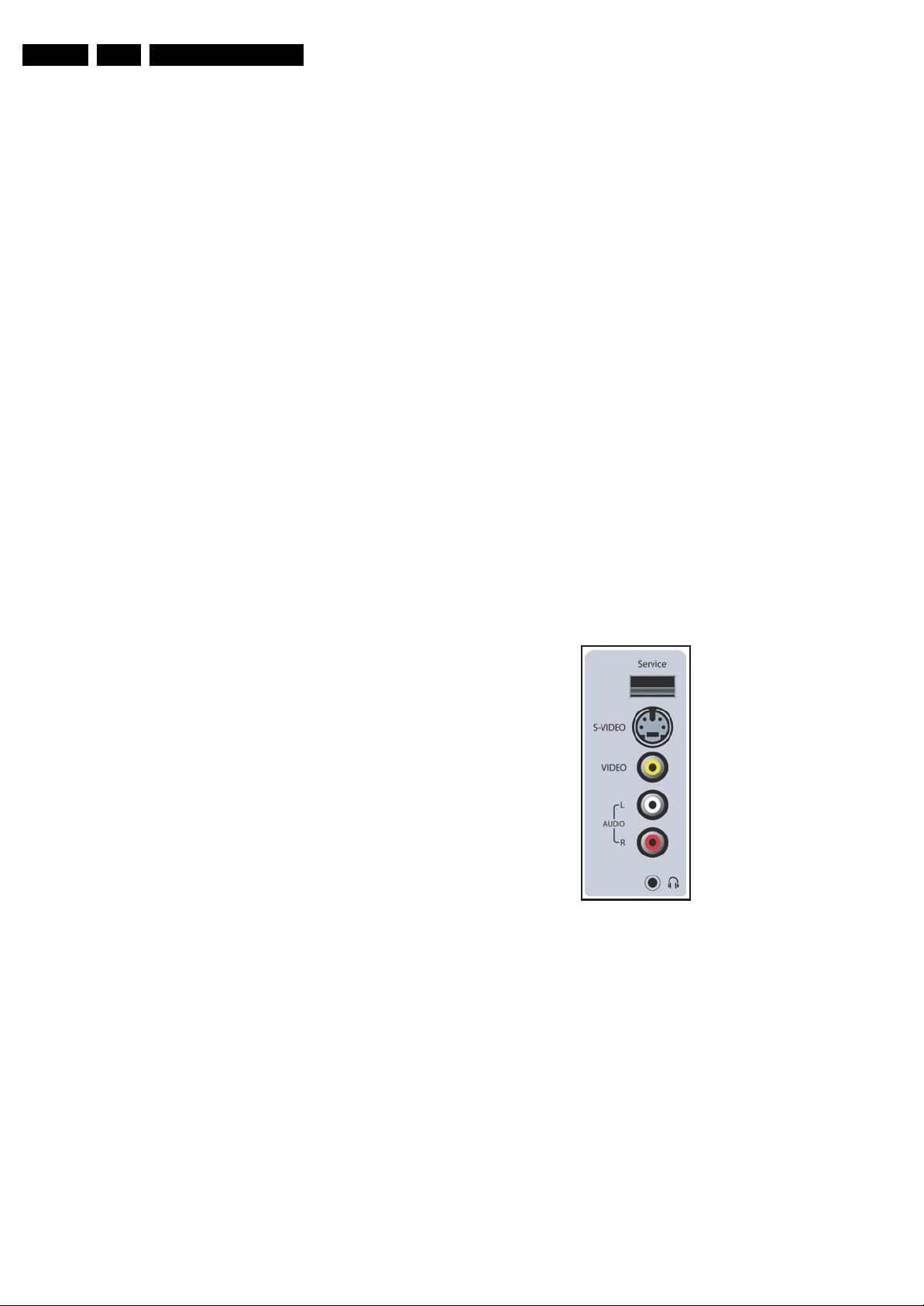
1.2.1 Side Connections
1.1.2 Sound
Sound systems : AV Stereo
Maximum power (W
1.1.3 Multimedia
USB input : USB1.1
) : 2 x 10
RMS
:BTSC
: Dolby Digital (AC3)
G_15870_025.eps
Figure 1-1 Side I/O connections
S-Video (Hosiden): Video Y/C - In
1 -Ground Y Gnd H
2 -Ground C Gnd H
3 -Video Y 1 V
4 -Video C 0.3 V
Cinch: Video CVBS - In, Audio - In
Ye - Video CVBS 1 V
Wh - Audio L 0.5 V
Rd - Audio R 0.5 V
100706
/ 75 ohm j
PP
P / 75 ohm j
PP
/ 75 ohm jq
PP
/ 10 kohm jq
RMS
/ 10 kohm jq
RMS
Mini Jack: Audio Headphone - Out
Bk - Headphone 32 - 600 ohm / 10 mW ot
Page 3
Technical Specifications, Connections, and Chassis Overview
EN 3CT2.0U RA 1.
USB1.1
1234
E_06532_022.eps
300904
Figure 1-2 USB (type A)
1-+5V k
2 -Data (-) jk
3 -Data (+) jk
4 -Ground Gnd H
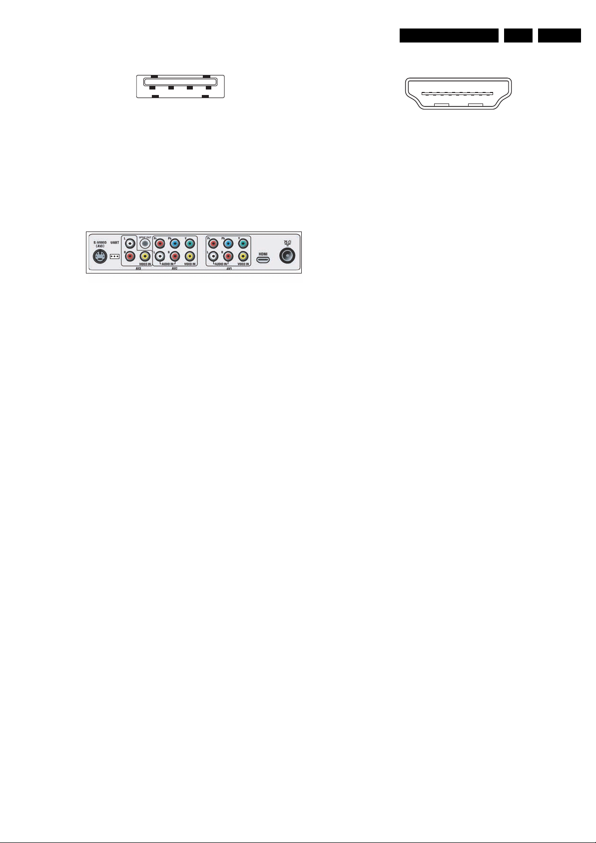
1.2.2 Rear Connections (under side)
Figure 1-3 Rear connections (under side)
AV3 S-Video (Hosiden): Video Y/C - In
1 -Ground Y Gnd H
2 -Ground C Gnd H
3 - Video Y 1 V
4 - Video C 0.3 V
/ 75 ohm j
PP
P / 75 ohm j
PP
Service Connector (UART)
1 - UART_TX Transmit k
2 - Ground Gnd H
3 - UART_RX Receive j
G_16570_024.eps
100706
HDMI 1: Digital Video, Digital Audio - In
19
1
18 2
E_06532_017.eps
250505
Figure 1-4 HDMI (type A) connector
1 - D2+ Data channel j
2 - Shield Gnd H
3 - D2- Data channel j
4 - D1+ Data channel j
5 - Shield Gnd H
6 - D1- Data channel j
7 - D0+ Data channel j
8 - Shield Gnd H
9 - D0- Data channel j
10 - CLK+ Data channel j
11 - Shield Gnd H
12 - CLK- Data channel j
13 - n.c.
14 - n.c.
15 - DDC_SCL DDC clock j
16 - DDC_SDA DDC data jk
17 - Ground Gnd H
18 - +5V j
19 - HPD Hot Plug Detect j
20 - Ground Gnd H
Aerial - In
- - F-type (US) Coax, 75 ohm D
AV3 Cinch: Audio - In
Wh - Audio L 0.5 V
Rd - Audio R 0.5 V
RMS
RMS
AV3 Cinch: Video CVBS - In
Ye - Video CVBS 1 V
/ 75 ohm jq
PP
Cinch: S/PDIF - Out
Bk - Coaxial 0.4 - 0.6V
AV2 Cinch: Video YPbPr - In
Gn - Video Y 1 V
Bu - Video Pb 0.7 V
Rd - Video Pr 0.7 V
/ 75 ohm jq
PP
PP
PP
AV2 Cinch: Video CVBS - In
Ye - Video CVBS 1 V
/ 75 ohm jq
PP
AV2 Cinch: Audio - In
Wh - Audio L 0.5 V
Rd - Audio R 0.5 V
RMS
RMS
AV1 Cinch: Video YPbPr - In
Gn - Video Y 1 V
Bu - Video Pb 0.7 V
Rd - Video Pr 0.7 V
/ 75 ohm jq
PP
PP
PP
AV1 Cinch: Video CVBS - In
Ye - Video CVBS 1 V
/ 75 ohm jq
PP
/ 10 kohm jq
/ 10 kohm jq
/ 75 ohm kq
PP
/ 75 ohm jq
/ 75 ohm jq
/ 10 kohm jq
/ 10 kohm jq
/ 75 ohm jq
/ 75 ohm jq
AV1 Cinch: Audio - In
Wh - Audio L 0.5 V
Rd - Audio R 0.5 V
/ 10 kohm jq
RMS
/ 10 kohm jq
RMS
Page 4
EN 4 CT2.0U RA1.
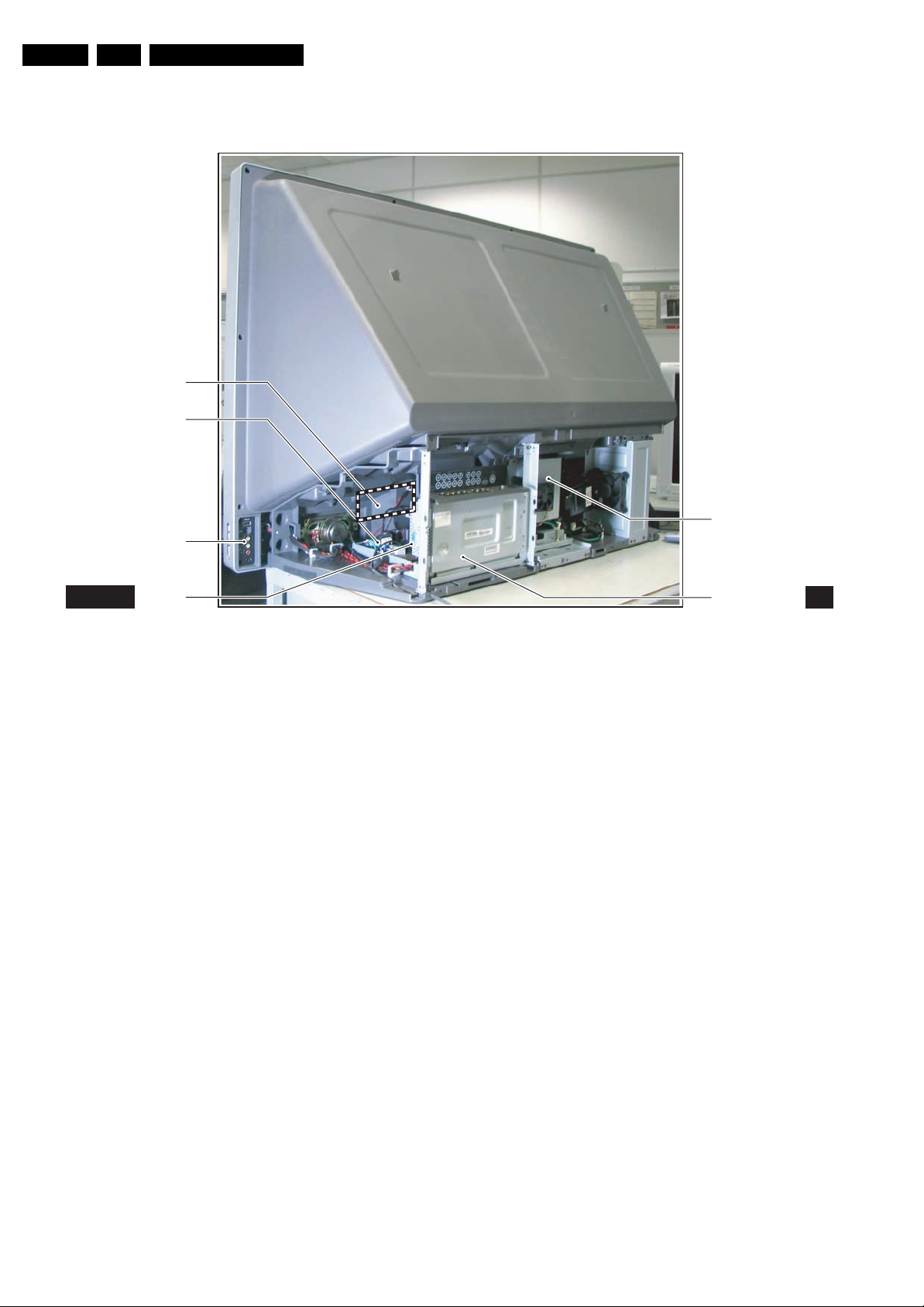
1.3 Chassis Overview
ON/OFF BUTTON
IR RECEIVER
POWER SUPLY
Technical Specifications, Connections, and Chassis Overview
KEYBOARD
MTV512
SIDE I/O
MTV512
BOARD
Figure 1-5 PWB/CBA locations
G_15870_026.eps
100706
LIGHT ENGINE
SMALL SIGNAL
BOARD
B
Page 5

Safety Instructions, Warnings, and Notes
2. Safety Instructions, Warnings, and Notes
EN 5CT2.0U RA 2.
Index of this chapter:
2.1 Safety Instructions
2.2 Warnings
2.3 Notes
2.1 Safety Instructions
Safety regulations require the following during a repair:
• Connect the set to the Mains/AC Power via an isolation
transformer (> 800 VA).
• Replace safety components, indicated by the symbol h,
only by components identical to the original ones. Any
other component substitution (other than original type) may
increase risk of fire or electrical shock hazard.
Safety regulations require that after a repair, the set must be
returned in its original condition. Pay in particular attention to
the following points:
• Route the wire trees correctly and fix them with the
mounted cable clamps.
• Check the insulation of the Mains/AC Power lead for
external damage.
• Check the strain relief of the Mains/AC Power cord for
proper function.
• Check the electrical DC resistance between the Mains/AC
Power plug and the secondary side (only for sets that have
a Mains/AC Power isolated power supply):
1. Unplug the Mains/AC Power cord and connect a wire
between the two pins of the Mains/AC Power plug.
2. Set the Mains/AC Power switch to the "on" position
(keep the Mains/AC Power cord unplugged!).
3. Measure the resistance value between the pins of the
Mains/AC Power plug and the metal shielding of the
tuner or the aerial connection on the set. The reading
should be between 4.5 Mohm and 12 Mohm.
4. Switch "off" the set, and remove the wire between the
two pins of the Mains/AC Power plug.
• Check the cabinet for defects, to prevent touching of any
inner parts by the customer.
2.2 Warnings
Service Default Mode (see chapter 5) with a colour bar
signal and stereo sound (L: 3 kHz, R: 1 kHz unless stated
otherwise) and picture carrier at 475.25 MHz for PAL, or
61.25 MHz for NTSC (channel 3).
• Where necessary, measure the waveforms and voltages
with (D) and without (E) aerial signal. Measure the
voltages in the power supply section both in normal
operation (G) and in stand-by (F). These values are
indicated by means of the appropriate symbols.
• The semiconductors indicated in the circuit diagram and in
the parts lists, are interchangeable per position with the
semiconductors in the unit, irrespective of the type
indication on these semiconductors.
2.3.2 Schematic Notes
• All resistor values are in ohms, and the value multiplier is
often used to indicate the decimal point location (e.g. 2K2
indicates 2.2 kohm).
• Resistor values with no multiplier may be indicated with
either an "E" or an "R" (e.g. 220E or 220R indicates 220
ohm).
• All capacitor values are given in micro-farads (µ= x10
nano-farads (n= x10
• Capacitor values may also use the value multiplier as the
decimal point indication (e.g. 2p2 indicates 2.2 pF).
• An "asterisk" (*) indicates component usage varies. Refer
to the diversity tables for the correct values.
• The correct component values are listed in the Spare Parts
List. Therefore, always check this list when there is any
doubt.
2.3.3 Rework on BGA (Ball Grid Array) ICs
General
Although (LF)BGA assembly yields are very high, there may
still be a requirement for component rework. By rework, we
mean the process of removing the component from the PWB
and replacing it with a new component. If an (LF)BGA is
removed from a PWB, the solder balls of the component are
deformed drastically so the removed (LF)BGA has to be
discarded.
-9
), or pico-farads (p= x10
-12
-6
),
).
• All ICs and many other semiconductors are susceptible to
electrostatic discharges (ESD w). Careless handling
during repair can reduce life drastically. Make sure that,
during repair, you are connected with the same potential as
the mass of the set by a wristband with resistance. Keep
components and tools also at this same potential. Available
ESD protection equipment:
– Complete kit ESD3 (small tablemat, wristband,
connection box, extension cable and earth cable) 4822
310 10671.
– Wristband tester 4822 344 13999.
• Be careful during measurements in the high voltage
section.
• Never replace modules or other components while the unit
is switched "on".
• When you align the set, use plastic rather than metal tools.
This will prevent any short circuits and the danger of a
circuit becoming unstable.
2.3 Notes
2.3.1 General
• Measure the voltages and waveforms with regard to the
chassis (= tuner) ground (H), or hot ground (I), depending
on the tested area of circuitry. The voltages and waveforms
shown in the diagrams are indicative. Measure them in the
Device Removal
As is the case with any component that, is being removed, it is
essential when removing an (LF)BGA, that the board, tracks,
solder lands, or surrounding components are not damaged. To
remove an (LF)BGA, the board must be uniformly heated to a
temperature close to the reflow soldering temperature. A
uniform temperature reduces the risk of warping the PWB.
To do this, we recommend that the board is heated until it is
certain that all the joints are molten. Then carefully pull the
component off the board with a vacuum nozzle. For the
appropriate temperature profiles, see the IC data sheet.
Area Preparation
When the component has been removed, the vacant IC area
must be cleaned before replacing the (LF)BGA.
Removing an IC often leaves varying amounts of solder on the
mounting lands. This excessive solder can be removed with
either a solder sucker or solder wick. The remaining flux can be
removed with a brush and cleaning agent.
After the board is properly cleaned and inspected, apply flux on
the solder lands and on the connection balls of the (LF)BGA.
Note: Do not apply solder paste, as this has been shown to
result in problems during re-soldering.
Device Replacement
The last step in the repair process is to solder the new
component on the board. Ideally, the (LF)BGA should be
Page 6
EN 6 CT2.0U RA2.
Safety Instructions, Warnings, and Notes
aligned under a microscope or magnifying glass. If this is not
possible, try to align the (LF)BGA with any board markers.
So as not to damage neighbouring components, it may be
necessary to reduce some temperatures and times.
More Information
For more information on how to handle BGA devices, visit this
URL: www.atyourservice.ce.philips.com (needs subscription,
not available for all regions). After login, select “Magazine”,
then go to “Repair downloads”. Here you will find Information
on how to deal with BGA-ICs.
2.3.4 Lead-free Solder
Philips CE is producing lead-free sets (PBF) from 1.1.2005
onwards.
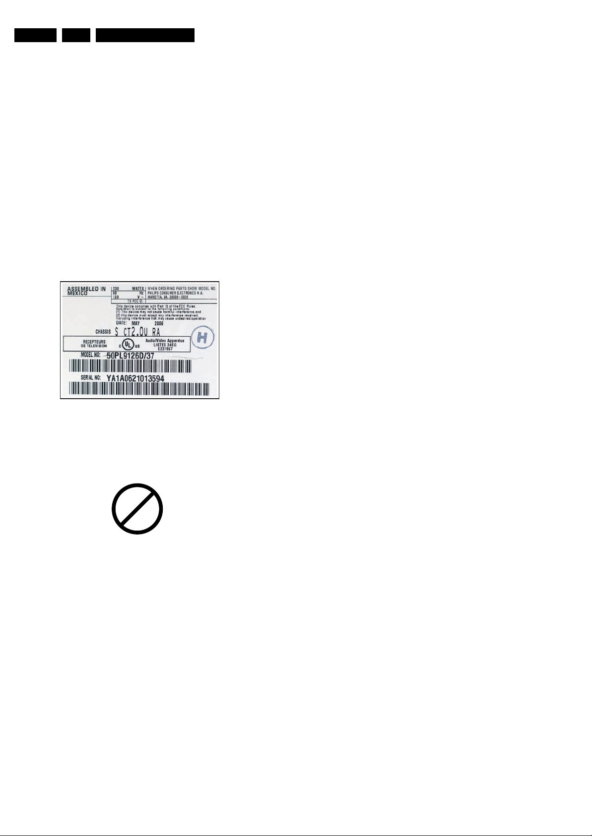
Identification: The bottom line of a type plate gives a 14-digit
serial number. Digits 5 and 6 refer to the production year, digits
7 and 8 refer to production week (in example below it is 1991
week 18).
G_15870_063.eps
Figure 2-1 Serial number example
Regardless of the special lead-free logo (which is not always
indicated), one must treat all sets from this date onwards
according to the rules as described below.
P
b
Figure 2-2 Lead-free logo
Due to lead-free technology some rules have to be respected
by the workshop during a repair:
• Use only lead-free soldering tin Philips SAC305 with order
code 0622 149 00106. If lead-free solder paste is required,
please contact the manufacturer of your soldering
equipment. In general, use of solder paste within
workshops should be avoided because paste is not easy to
store and to handle.
• Use only adequate solder tools applicable for lead-free
soldering tin. The solder tool must be able:
– To reach a solder-tip temperature of at least 400°C.
– To stabilise the adjusted temperature at the solder-tip.
– To exchange solder-tips for different applications.
• Adjust your solder tool so that a temperature of around
360°C - 380°C is reached and stabilised at the solder joint.
Heating time of the solder-joint should not exceed ~ 4 sec.
Avoid temperatures above 400°C, otherwise wear-out of
tips will increase drastically and flux-fluid will be destroyed.
To avoid wear-out of tips, switch “off” unused equipment or
reduce heat.
• Mix of lead-free soldering tin/parts with leaded soldering
tin/parts is possible but PHILIPS recommends strongly to
100706
avoid mixed regimes. If this cannot be avoided, carefully
clear the solder-joint from old tin and re-solder with new tin.
• Use only original spare-parts listed in the Service-Manuals.
Not listed standard material (commodities) has to be
purchased at external companies.
• Special information for lead-free BGA ICs: these ICs will be
delivered in so-called "dry-packaging" to protect the IC
against moisture. This packaging may only be opened
shortly before it is used (soldered). Otherwise the body of
the IC gets "wet" inside and during the heating time the
structure of the IC will be destroyed due to high (steam-)
pressure inside the body. If the packaging was opened
before usage, the IC has to be heated up for some hours
(around 90°C) for drying (think of ESD-protection!).
Do not re-use BGAs at all!
• For sets produced before 1.1.2005, containing leaded
soldering tin and components, all needed spare parts will
be available till the end of the service period. For the repair
of such sets nothing changes.
In case of doubt whether the board is lead-free or not (or with
mixed technologies), you can use the following method:
• Always use the highest temperature to solder, when using
SAC305 (see also instructions below).
• De-solder thoroughly (clean solder joints to avoid mix of
two alloys).
Caution: For BGA-ICs, you must use the correct temperatureprofile, which is coupled to the 12NC. For an overview of these
profiles, visit the website www.atyourservice.ce.philips.com
(needs subscription, but is not available for all regions)
You will find this and more technical information within the
"Magazine", chapter "Repair downloads".
For additional questions please contact your local repair help
desk.
2.3.5 Alternative BOM identification
In September 2003, Philips CE introduced a change in the way
the serial number (or production number, see Figure 2-1) is
composed. From this date on, the third digit in the serial
number (example: AG2B0335000001) indicates the number of
the alternative BOM (Bill of Materials used for producing the
specific model of TV set). It is possible that the same TV model
on the market is produced with e.g. two different types of
displays, coming from two different O.E.M.s.
By looking at the third digit of the serial number, the service
technician can see if there is more than one type of B.O.M.
used in the production of the TV set he is working with. He can
then consult the At Your Service Web site, where he can type
in the Commercial Type Version Number of the TV set (e.g.
28PW9515/12), after which a screen will appear that gives
information about the number of alternative B.O.M.s used.
If the third digit of the serial number contains the number 1
(example: AG1B033500001), then there is only one B.O.M.
version of the TV set on the market. If the third digit is a 2
(example: AG2B0335000001), then there are two different
B.O.M.s. Information about this is important for ordering
the correct spare parts!
For the third digit, the numbers 1...9 and the characters A...Z
can be used, so in total: 9 plus 26 = 35 different B.O.M.s can
be indicated by the third digit of the serial number.
2.3.6 Practical Service Precautions
• It makes sense to avoid exposure to electrical shock.
While some sources are expected to have a possible
dangerous impact, others of quite high potential are of
limited current and are sometimes held in less regard.
• Always respect voltages. While some may not be
dangerous in themselves, they can cause unexpected
reactions that are best avoided. Before reaching into a
powered TV set, it is best to test the high voltage insulation.
It is easy to do, and is a good service precaution.
Page 7

3. Directions for Use
You can download this information from the following websites:
http://www.philips.com/support
http://www.p4c.philips.com
Directions for Use
EN 7CT2.0U RA 3.
Page 8
EN 8 CT2.0U RA4.
Mechanical Instructions
4. Mechanical Instructions
Index of this chapter:
4.1 Cable Dressing
4.2 Assy/Panel Removal
4.3 Set Re-assembly
4.1 Cable Dressing
Notes:
• Several models in this chassis range have a different
mechanical construction, the instructions given in this
chapter are therefore very model specific.
• Figures below can deviate slightly from the actual situation,
due to the different set executions.
• Follow the disassemble instructions in described order.
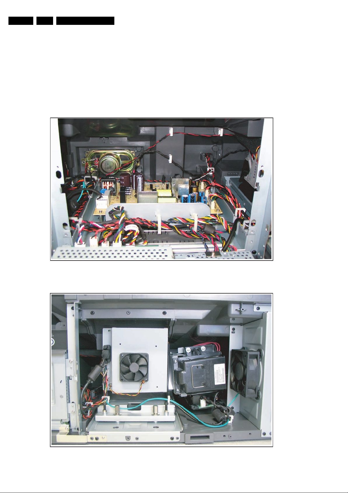
Figure 4-1 Cable dressing 1/3 (PSU etc., SSB/MTV module detached from the frame)
G_16570_065.eps
100706
Figure 4-2 Cable dressing 2/3 (Light Engine, rear)
G_16570_066.eps
100706
Page 9
Mechanical Instructions
EN 9CT2.0U RA 4.
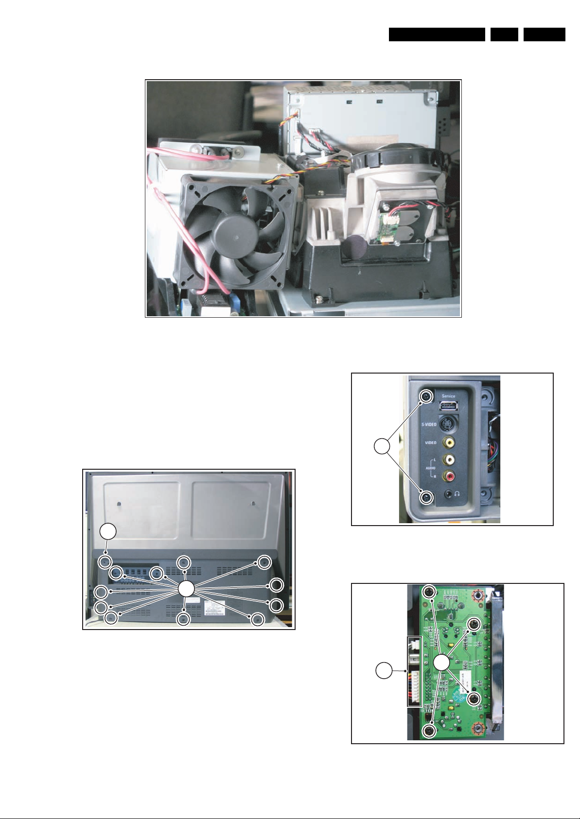
Figure 4-3 Cable dressing 3/3 (Light Engine, front)
4.2 Assy/Panel Removal
4.2.1 Rear Cover
Caution: Disconnect the Mains/AC Power cord before you
remove the rear cover!
1. Remove fixation screws [1].
2. Remove the rear cover.
1
1
G_16570_067.eps
100706
1
G_15870_028.eps
Figure 4-5 Keyboard / Side I/O module removal
070706
Figure 4-4 Rear cover removal
4.2.2 Keyboard / Side I/O Panel
1. Remove the rear cover, as described previously.
2. Remove screws [1].
3. Take out the module.
4. Unplug connectors [2].
5. Remove screws [3].
When defective, replace the whole unit.
G_15870_027.eps
070706
2
3
G_15870_029.eps
Figure 4-6 Keyboard / Side I/O panel removal
110706
Page 10
EN 10 CT2.0U RA4.
Mechanical Instructions
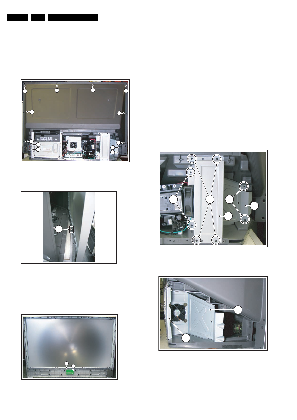
4.2.3 Front Cover
1. Remove the rear cover, as described previously.
2. Remove the keyboard / side I/O panel.
3. Remove screws [1].
4. ‘Open’ the front cover just far enough to gain access to the
connector [2] of the on/off button / IR receiver panel.
5. Unplug connector [2].
6. Carefully remove the front cover and put it in a safe place.
1
1
1
1
1
1
1
1
1
1
1
1
G_15870_030.eps
070706
4.2.5 Right Speaker
1. Remove the rear cover, as described previously.
2. Unplug the connectors.
3. Remove the fixation screws.
4. Remove the speaker.
4.2.6 Left Speaker
1. Remove the rear cover, as described previously.
2. Remove screws [1].
3. Loosen screws [2] for approx. 3 turns.
4. Remove screws [3].
5. Pull fan bracket [4] towards you, against the heads of
screws [2].
6. Pull air duct [5] gently towards you, to create a wider
access to the speaker.
7. Unplug the connectors from the speaker.
8. Remove the fixation screws of the speaker.
9. Remove the speaker.
10. After replacement, carefully position air duct [5] and fan
bracket [4] before you tighten the screws. The positioning
pins near screws [1] must be correctly in place.
Figure 4-7 Front cover removal 1/2
2
Figure 4-8 Front cover removal 2/2
4.2.4 Power Switch / IR Receiver Board
1. Remove the front cover, as described previously.
2. Remove screws [1].
G_15870_031.eps
070706
21 3
Figure 4-10 Air duct 1/2
5
4
G_15870_033.eps
100706
5
1
1
G_15870_032.eps
Figure 4-9 Power switch / IR receiver board
070706
4
Figure 4-11 Air duct 2/2
G_15870_034.eps
070706
Page 11
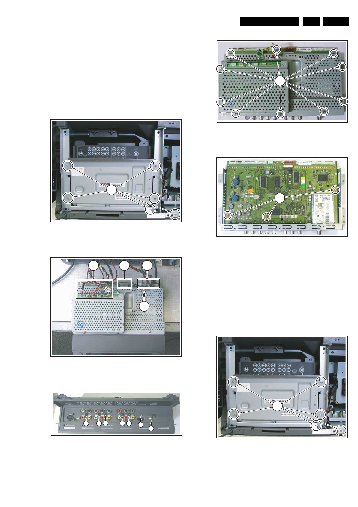
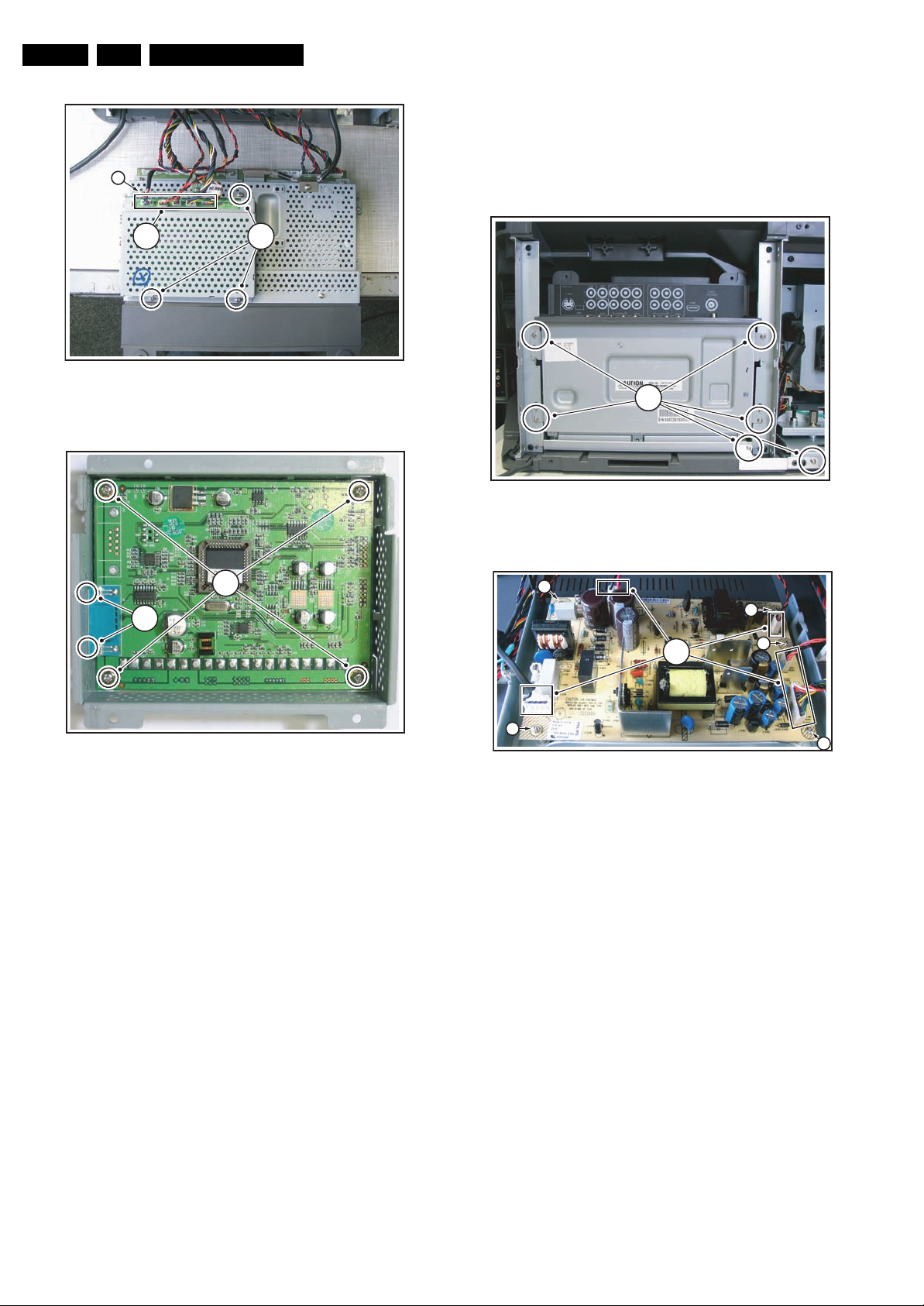
4.2.7 Small Signal Board (SSB)
1. Remove the rear cover, as described previously.
2. Remove screws [1].
3. Take out the SSB assy and put it directly behind the set.
4. Remove screw [2].
5. Carefully unplug the fragile LVDS connector [3].
6. Unplug connectors [4].
7. Remove screws [5] and nut [6].
8. Remove screws [7].
9. Lift the shield (together with the MTV512 module) from the
SSB module.
10. Remove screws [8].
1
Mechanical Instructions
7
Figure 4-15 SSB top shield
8
EN 11CT2.0U RA 4.
G_15870_038.eps
070706
Figure 4-12 SSB fixation
4 3 4
Figure 4-13 SSB connectors
G_15870_035.eps
2
G_15870_036.eps
070706
110706
Figure 4-16 SSB board
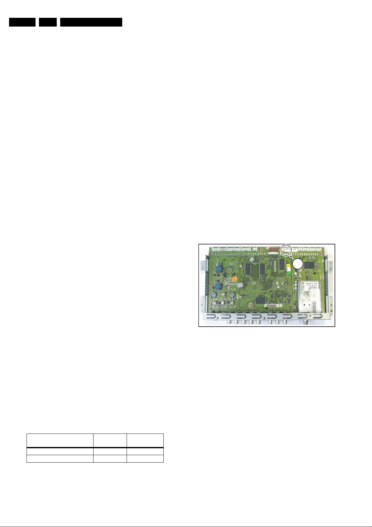
4.2.8 Micro Processor Board (MTV512)
1. Remove the rear cover, as described previously.
2. Remove screws [1].
3. Take out the SSB assy and put it directly behind the set.
4. Unplug connectors [2].
5. Remove screws [3].
6. Lift the MTV module from the SSB module.
7. Remove fixation screws [4] from the serial connector.
8. Remove screws [5].
G_15870_039.eps
100706
5 5 5 5 5
Figure 4-14 SSB I/O panel
5
6
G_15870_037.eps
070706
1
Figure 4-17 SSB fixation
G_15870_035.eps
070706
Page 12
EN 12 CT2.0U RA4.
Mechanical Instructions
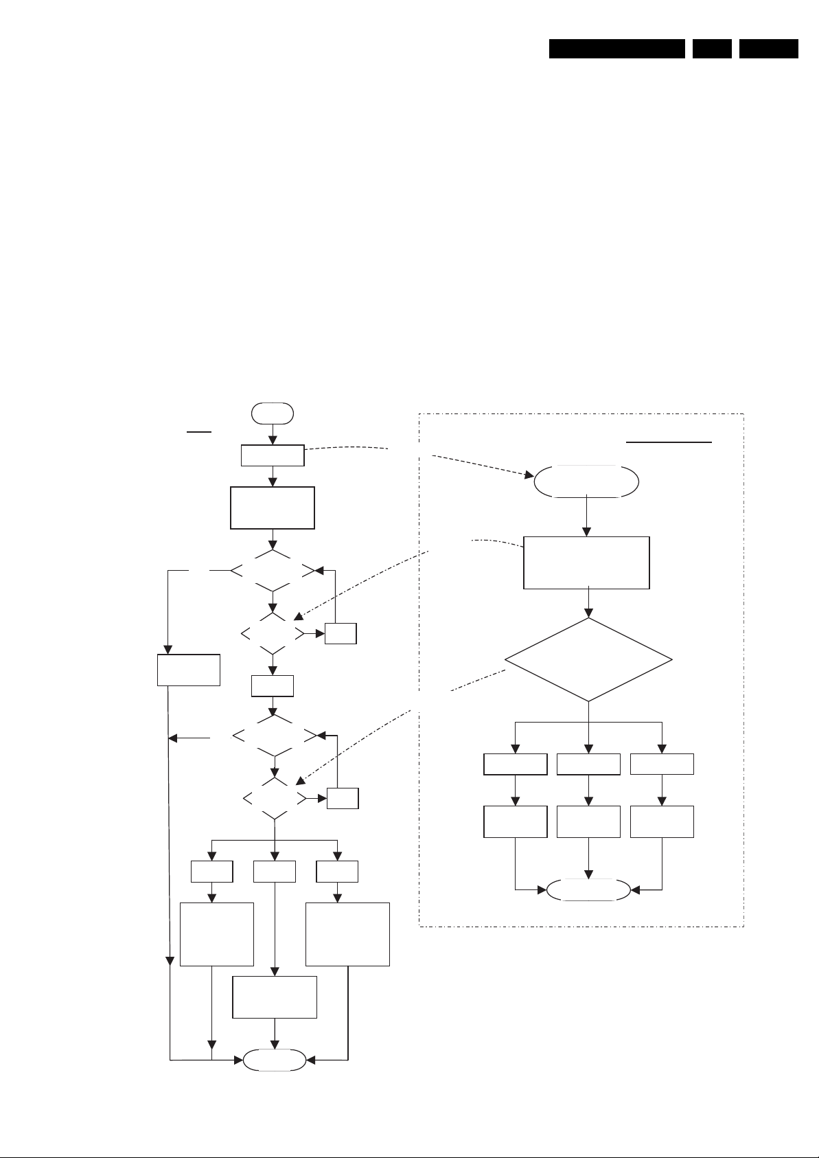
4.2.9 Power Supply Unit (PSU)
1. Remove the rear cover, as described previously.
2. Remove screws [1].
3. Take out the SSB assy and put it directly behind the set.
3
4. Unplug connectors [2].
5. Remove screws [3].
2
3
Figure 4-18 MTV512 module
5
4
G_15870_040.eps
100706
Figure 4-20 SSB fixation
3
1
G_15870_035.eps
070706
3
2
3
Figure 4-19 MTV512 board
G_15870_041.eps
100706
3
Figure 4-21 Power supply unit
G_15870_042.eps
3
100706
Page 13

Mechanical Instructions
EN 13CT2.0U RA 4.
4.2.10 Projection Screen Removal
1. Remove the front cover, as described previously.
2. Remove screws [1].
3. Remove the fixation strips [2].
1 1 1 1 1 1 1 1
1
1
2
1
1
Figure 4-22 Projection screen
4.2.11 Projection Lamp Replacement
1. Remove the rear cover, as described previously.
2. Remove screws [1].
3. Pull out the lamp unit with grip [2].
4. Remove nut and lock washer [3].
5. Remove screws [4].
1
1
1
1111111
G_15870_043.eps
100706
4.2.12 Light Engine Removal
1. Remove rear cover, as described previously.
2. Unplug connectors [1].
3. Remove screws [2].
4. Pull the light engine out of the set.
2 2
1
2
2 2
Figure 4-25 Light engine
4.3 Set Re-assembly
To re-assemble the whole set, execute all processes in reverse
order.
G_15870_046.eps
100706
1
Figure 4-23 Projection lamp 1/2
4
3
2
G_15870_044.eps
Notes:
• While re-assembling, make sure that all cables are placed
and connected in their original position. See figures "Cable
dressing".
• Pay special attention not to damage the EMC foams on the
SSB shields. Ensure that EMC foams are mounted
correctly.
100706
4
Figure 4-24 Projection lamp 2/2
G_15870_045.eps
100706
Page 14
EN 14 CT2.0U RA5.
Service Modes, Error Codes, and Fault Finding
5. Service Modes, Error Codes, and Fault Finding
Index of this chapter:
5.1 Test Points
5.2 Service Modes
5.3 Stepwise Start-up
5.4 Service Tools
5.5 Error Codes
5.6 The Blinking LED Procedure
5.7 Protections
5.8 Fault Finding and Repair Tips
5.9 Software Upgrading
5.1 Test Points
As most signals are digital, it will be almost impossible to
measure waveforms with a standard oscilloscope. Therefore,
waveforms are not given in this manual. Several key ICs are
capable of generating test patterns, which can be controlled via
ComPair. In this way it is possible to determine which part is
defective.
Perform measurements under the following conditions:
• Service Default Mode.
• Video: Color bar signal.
• Audio: 3 kHz left, 1 kHz right.
5.2 Service Modes
Service Default Mode (SDM) and Service Alignment Mode
(SAM) offer several features for the service technician, while
the Customer Service Mode (CSM) is used for communication
between a Customer Helpdesk and a customer.
There is also the option of using ComPair, a hardware interface
between a computer (see requirements below) and the TV
chassis. It offers the ability of structured troubleshooting, test
pattern generation, error code reading, software version
readout, and software upgrading.
Minimum requirements for ComPair: a Pentium processor,
Windows 95/98, and a CD-ROM drive (see also paragraph
“ComPair”).
in the channel map and could be different from the one
corresponding to the physical channel 3.
• All picture settings at 50% (brightness, color, contrast).
• All sound settings at 50%, except volume at 25%.
• All service-unfriendly modes (if present) are disabled, like:
– (Sleep) timer.
– Child/parental lock.
– Picture mute (blue mute or black mute).
– Automatic volume levelling (AVL).
– Auto switch "off" (when no video signal was received
for 10 minutes).
– Skip/blank of non-favorite pre-sets.
– Smart modes.
– Auto store of personal presets.
– Auto user menu time-out.
How to Activate SDM
Use one of the following methods:
• Use the standard RC-transmitter and key in the code
“062596”, directly followed by the “MENU” button.
Note: It is possible that, together with the SDM, the main
menu will appear. To switch it "off", push the “MENU”
button again.
• Short for a moment the two solder pads [1] on the SSB,
with the indication “SDM” (on the picture they are located
underneath the sticker). They are located outside the
shielding. Activation can be performed in all modes, except
when the set has a problem with the Stand-by Processor.
See figure “SDM and SPI service pads”.
1
5.2.1 Service Default Mode (SDM)
Purpose
• To create a pre-defined setting, to get the same
measurement results as given in this manual.
• To override SW protections (only applicable for protections
detected by stand-by processor) and make the TV start up
to the step just before protection (a sort of automatic
stepwise start up). See paragraph “Stepwise Start Up”.
• To start the blinking LED procedure (not valid in protection
mode).
Specifications
Table 5-1 SDM default settings
Region Freq. (MHz)
Europe, AP-PAL/Multi 475.25 PAL B/G
NAFTA, AP-NTSC, LATAM 61.25 (ch. 3) NTSC M
• Tuning frequency 61.25 MHz for NTSC: The TV shall tune
to physical channel 3 only if channel 3 is an analog channel
or if there is no channel 3 installed in the channel map. If
there is a digital channel installed in channel 3, then the
frequency to which the set will tune, would be as specified
Default
system
Figure 5-1 SDM and SPI service pads
After activating this mode, “SDM” will appear in the upper right
corner of the screen (if you have picture).
How to Navigate
When you press the “MENU” button on the RC transmitter, the
set will toggle between the SDM and the normal user menu
(with the SDM mode still active in the background).
How to Exit SDM
Use one of the following methods:
• Switch the set to STAND-BY via the RC-transmitter.
• Via a standard customer RC-transmitter: key in “00”sequence.
5.2.2 Service Alignment Mode (SAM)
Purpose
• To perform (software) alignments.
• To change option settings.
• To easily identify the used software version.
• To view operation hours.
• To display (or clear) the error code buffer.
G_15870_047.eps
100706
Page 15

Service Modes, Error Codes, and Fault Finding
EN 15CT2.0U RA 5.
How to Activate SAM
Via a standard RC transmitter: key in the code “062596”
directly followed by the “INFO” button. After activating SAM
with this method, a service warning will appear on the screen,
SAM-menu
Hardware info A. SW version
Operation hours 289
Errors No Errors
Defective module
Reset error buffer Start now
Alignments General Tuner AGC 32
Dealer options
Options
Initialise NVM
Store
SW maintenance
DLP Menu
ED10U-1.0.1.0_07892
B. SBY PROC version
001.008.002.014
C. Production code
YA1A0621013594
Whitepoint Color temperature
Personal options
PIP/DS
Data
Display
Video repro Picture processing
Source selection
Audio repro Subwoofer internal present Off / On
Miscellaneous
Option numbers Group 1 00016 00000 00033 14979
Store (completed)
SW events
HW events
DLP Status
DLP Setting
White point red
White point green
White point blue
Red BL offset
Green BL offset
Picture mute
Virgin mode
2 CS Korea
Dualscreen
EPG
RRT
Screen
Scanning backlight
Dimming backlight
Comb filter
Ambient light
MOP
HDMI1 None / With analog audio / Without analog audio
HDMI2 None / With analog audio / Without analog audio
USB version
IEEE1394 Not present
Ethernet
SPDIF inputs
Acoustic system
Alternative tuner
Tuner type
Hotel mode
Group 2 00038 00000 00544 00000
Store
Display
Clear
Test reboot
Display
Clear
Thermal Degree
Fan1 Rotation Rate
Fan2 Rotation Rate
Lamp Life
MTV512 MCU Version
Bright-R 0
Bright-G 0
Bright-B 0
Contrast-R 100
Contrast-G 100
Contrast-B 100
Reset lamp life
Gamma
Test Pattern Ok
you can continue by pressing the red button on the RC. Then
you have access to the following menu:
Normal / Warm / Cool
127
127
127
7
7
Off / On
Off / On
Off
None / One tuner ds / Two tuner ds
Off / On
No / Yes
038 (50” Coretronic DLP)
Off / On
Off / On
No spider
None / 2D comb / 3D comb
Off / Mono / Stereo
Off / On
None / USB 1.1 / USB 2.0 + Cardreader
Off
None / 1 connector / 2 connectors
None / ... / 50DLP / 60DLP
Philips
TD1336s
Off
Store (completed)
Start now (push OK to view log-file)
Start now (push OK to clear log-file)
Start now (push OK to reboot)
Start now (push OK to view log-file)
Start now (push OK to clear log-file)
33
NORMAL
NORMAL
162 H
A18
Ok
Film / Graphic / Video
G_15870_064.eps
100706
Figure 5-2 SAM menu
Page 16

EN 16 CT2.0U RA5.
Contents of SAM:
• Hardware Info.
– A. VIPER SW Version. Displays the software version
of the VIPER software (main software) (example:
ED10U-1.2.3.4_12345 = AAAAB_X.Y.W.Z_NNNNN).
• AAAA= the chassis name.
• B= the region: A= AP, E= EU, L= Latam, U = US.
• X.Y.W.Z= the software version, where X is the
main version number (different numbers are not
compatible with one another) and Y is the sub
version number (a higher number is always
compatible with a lower number). The last two
digits are used for development reasons only, so
they will always be zero in official releases.
• NNNNN= last five digits of 12nc code of the
software.
– B. SBY PROC Version. Displays the software version
of the stand-by processor.
– C. Production Code. Displays the production code of
the TV, this is the serial number as printed on the back
of the TV set. Note that if an NVM is replaced or is
initialized after corruption, this production code has to
be re-written to NVM. ComPair will foresee in a
possibility to do this.
• Operation Hours. Displays the accumulated total of
operation hours (not the stand-by hours). Every time the
TV is switched "on/off", 0.5 hours is added to this number.
• Errors. (Followed by maximal 10 errors). The most recent
error is displayed at the upper left (for an error explanation
see paragraph “Error Codes”).
• Defective Module. Here the module that generates the
error is displayed. If there are multiple errors in the buffer,
which are not all generated by a single module, there is
probably another defect. It will then display the message
“UNKNOWN” here.
• Reset Error Buffer. When you press “cursor right” and
then the “OK” button, the error buffer is reset.
• Alignments. This will activate the “ALIGNMENTS” submenu.
• Dealer Options. Extra features for the dealers.
• Options. Extra features for Service.
• Initialise NVM. When an NVM was corrupted (or replaced)
in the former EMG based chassis, the microprocessor
replaces the content with default data (to assure that the
set can operate). However, all preferences and alignment
values are gone now, and option numbers are not correct.
Therefore, this was a very drastic way. In this chassis, the
procedure is implemented in another way: The moment the
processor recognizes a corrupted NVM, the “initialize
NVM” line will be highlighted. Now, you can do two things
(dependent of the service instructions at that moment):
– Save the content of the NVM via ComPair for
development analysis, before initializing. This will give
the Service department an extra possibility for
diagnosis (e.g. when Development asks for this).
– Initialize the NVM (same as in the past, however now it
happens conscious).
Service Modes, Error Codes, and Fault Finding
Note: When you have a corrupted NVM, or you have replaced
the NVM, there is a high possibility that you will not have picture
any more because your display option is not correct. So, before
you can initialize your NVM via the SAM, you need to have a
picture and therefore you need the correct display option. To
adapt this option, use ComPair. The correct HEX values for the
options can be found in the table below.
Page 17
Service Modes, Error Codes, and Fault Finding
(
(8)
(A1)
(8)
g
g
g
(V3)
g
g
(A2)
(
)
g
p
(
g)
(
)
(8)
(8)
(8)
(8)
(A3)
(
)
g)
g
p
(
)
(
)
(
g)
p
p
EN 17CT2.0U RA 5.
Display
option
000 00 PDP SDI 42” 768p 1024
001 01 PDP SDI 50” 768p 1366
002 02 PDP FHP 42” 1024i 1024
003 03 LCD LPL 30” 768p 1280 LC300W01-A3P7 9322 198 00682 analo
004 04 LCD LPL 37” 768p 1366 LC370W01-A6 9322 220 87682 analo
005 05 LCD LPL 42” 768p 1366 LC420W02-A6 9322 226 39682 analo
006 06 LCD Sharp 32” 768p 1366 LQ315T3LZ13 (ASV1)
007 07 PDP SDI 42” 480p 852
008 08 PDP FHP 37” 1024i 1024
009 09 LCOS XION 720p 1280 n.a. n.a. NA 8
010 0A LCD AUO 30” 768p 1280
011 0B LCD LPL 32” 768p 1366 LC320W01-A6K1 9322 217 44682 analo
012 0C LCD AUO 32” 768p 1366 T315XW01V5 9322 231 69682 PWM 8
013 0D LCD Sharp 37” 768p 1366 LQ370T3LZ21 (ASV2)
014 0E LCD LPL 42” X 1080p 1920 LC420WU1-SL01 9322 228 99682 PWM 8
015 0F PDP SDI 37” 480p 852
016 10 PDP FHP 37” 1080i 1024
017 11 PDP FHP 42” 1080i 1024
018 12 PDP FHP 55” 768p 1366
019 13 LCOS VENUS 720p 1280 n.a. n.a. NA
020 14 LCOS VENUS X 1080p 1920 n.a. n.a. NA
021 15 LCD LPL 26” 768p 1366 LC260WX2-SL01 9322 221 01682 PWM 8 S *
022 16 LCD LPL 32” X 768p 1366 LC320WX2-SL01
023 17 PDP LGE 42” 480p 852
024 18 PDP SDI 42” 480p 852
025 19 PDP SDI 42” 768p 1024
026 1A PDP FHP 42” 1024i 1024
027 1B PDP SDI 50” 768p 1366
028 1C LCD Sharp 37” X 1080P 1920 LQ370D3LZ13
029 1D LCD AUO 32” 768p 1366 T315XW01-V3
030 1E LCD Sharp 37” X X 1080p 1920 LW370D3LZ1x (ASV 3 first samples) not used PWM 10(8) X
031 1F LCD Sharp 37” X X 1080P 1920 LK370D3LZ33
032 20 LCD LPL 20” 768p 1366 LC200WX1-SL01 9322 222 90682 tbd S
033 21 LCD QDI 23” 768p 1366
034 22 ECO PTV 51” 1080i 1366 ? NA n.a.
035 23 ECO PTV 55” 1080i 1366 ? NA n.a.
036 24 ECO PTV 61” 1080i 1366 ? NA n.a.
037 25 PDP FHP 42” 1024I 1024
038 26 DLP 50” 720p 1280 ? NA 10 S
039 27 DLP 60” 720p 1280 ? NA 10 S
040 28 LCD Sharp 32” 768p 1366 LK315T3LZ43
041 29 LCD LPL 42” X 768p 1366 LC420W X2-SLA1 9322 240 80682 analo
042 2A PDP SDI 63” 768p 1366
043 2B LCD Sharp 37” X 768p 1366 LK370T3LZ63
044 2C LCD Sharp 37” 768p 1366 LK370T3LZ53
045 2D LCD LPL 26” 768p 1366 LC260WX2-SLB2 9322 234 13682 PWM 8 X
046 2E LCD LPL 32” 768 p 1366 LC320W01-SL06 9322 230 03682 PWM 8 S
047 2F LCD LPL 42” 768p 1366 LC420W02-SLB1 9322 234 12682 PWM 8 X
048 30 LCD QDI 26” 768p 1366 QD26HL02-REV01
049 31 LCD AUO 26” 768p 1366 T260XW02V4 9322 231 90682 PWM 8 X
050 32 LCD AUO 32” 768p 1366 T315XW01V9 9322 231 89682 PWM 8 S
051 33 LCD AUO 37” 768p 1366 T370XW01V1 9322 233 78682 PWM 8 S
052 34 LCD AUO 32” 768p 1366 T315XW02V5
053 35 LCD LPL 37” 768p 1366 LC370WX1-SL04 9322 233 19682 PWM 8 S
054 36 PDP LGE 42” 768p 1024
055 37 LCD LPL 42" X 1080p 1920
056 38 LCD LPL 47" X 1080p 1920 PWM X
057
058
059
060 3C LCD Tbd ? X 768p 1366
061 3C LCD Tbd ? X 768p 1366
HEX
Display type
Brand SIZE
Full HDClear
LCD
Resolution
vertical
Resolution
horizontal
Code number 12 NC
S42AX-YD01
PP42AX-007A) 9322 225 38682
S50HW-XD03 9322 215 26682
FPF42C128128UC-52
LQ315T3LZ23 (ASV2.2)(5Vtcon)
LQ315T3LZ23 (ASV2.2)(12Vtcon)
S42SD-YD05
FPF37C128128UB-72 9322 217 56682
T296XW01
T296XW01V2
T296XW01V3
LQ370T3LZ44 (ASV2.2)
S37SD-YD02 9322 217 39682
not used not used
FPF42C128135UA-52 9322 235 43682
not used not used
not used not used
S42SD-YD07(PP42SD-015A) (V4)
S42SD-YD07(PP42SD-015B) (V4)
S42SD-YD07(PP42SD-015F) (V4)
S42AX-YD01(PP42AX-007A) (V4)
S42AX-YD01(PP42AX-008A) (V4)
S42AX-YD01(PP42AX-008B) (V4)
S42AX-YD02(PP42AX-009A) (W1)
FPF42C128128UD-51
S50HW-XD04(PP50HW-005A) (V4)
S50HW-XD04(PP50HW-005B) (V4)
S50HW-XD04(PP50HW-005E) (V4)
S50HW-YD01(PP50HW-010A) (W1)
QD23HL02 REV01
QD23HL02 REV01(03)
FPF42C128135UA-52
S63HW-XD04 see
QD26HL02-REV02
PDP42X3 see
LC420WU2-SLA1 8204 001 50441
100/120Hz 1
100/120Hz final
st
silicon
ASV2.2
ASV 3
ASV 2.3
ASV 3
ASV 2.3
9322 235 43682
Dimming
NA 8
NA 10
9322 212 78682
9322 209 35682
9322 226 58682
9322 226 16682
9322 215 27682
9322 206 49682
9322 219 45682
9322 213 33682
? analog 8
9322 241 46682
9322 226 37682
9322 226 96682
9322 233 81682
9322 225 38682
9322 226 95682
9322 233 80682
9322 240 08682
not used
9322 226 54682
9322 226 97682
9322 233 79682
9322 240 25682
9322 228 48682 analo
see
artslist for 12NC
9322 242 22682
9322 223 91682
9322 232 69682
9322 235 32682 PWM (analo
artslist for 12NC
see partslist for 12NC
9322 235 83682
9322 227 29682
9322 235 05682
see
artslist for 12NC
artslist for 12NC
NA 10
analog 8
NA 8
NA 10
analog 8
NA
NA
NA X
NA 10
analo
NA 8
NA 10 (8) X
NA 10 (8) X X
NA 8
NA 10(8) X X
PWM
PWM 10
tbd S
NA
NA X
PWM
PWM
PWM 8 S
PWM 8 X
NA 10 X
PWM X
PWM 10 X
PWM 10 X
bits (1)
analo
analo
Nr. of
2k5 2k6
full
8
8X
8X
8X
8X
10(8)X
8X
XX
8X
XX
XX
2k6
baby
2k7
S
S
S
Figure 5-3 Display type table
• Store. All options and alignments are stored when
pressing “cursor right” and then the “OK”-button
• SW Maintenance.
– SW Events. Not useful for service purposes. In case of
specific software problems, the development
department can ask for this info.
– HW Events. Not functional at the moment this manual
is released, description will be published in an update
manual if the function becomes available.
• Operation hours PDP. Displays the accumulated total of
PDP operation hours.
How to Navigate
• In SAM, you can select the menu items with the “CURSOR
UP/DOWN” key on the RC-transmitter. The selected item
will be highlighted. When not all menu items fit on the
screen, move the “CURSOR UP/DOWN” key to display the
next/previous menu items.
E_06532_030.eps
220606
• With the “CURSOR LEFT/RIGHT” keys, it is possible to:
– (De) activate the selected menu item.
– (De) activate the selected submenu.
How to Exit SAM
Use one of the following methods:
• Press the “MENU” button on the RC-transmitter.
• Switch the set to STAND-BY via the RC-transmitter.
Note: As long as SAM is activated, it is not possible to change
a channel. This could hamper the White Point alignments
because you cannot choose your channel/frequency any more.
Workaround: after you have sent the RC code “062596 INFO”
you will see the service-warning screen, and in this stage it is
still possible to change the channel (so before pressing the
“OK” button).
Page 18

EN 18 CT2.0U RA5.
Service Modes, Error Codes, and Fault Finding
5.2.3 Customer Service Mode (CSM)
Purpose
When a customer is having problems with his TV-set, he can
call his dealer or the Customer Helpdesk. The service
technician can then ask the customer to activate the CSM, in
order to identify the status of the set. Now, the service
technician can judge the severity of the complaint. In many
cases, he can advise the customer how to solve the problem,
or he can decide if it is necessary to visit the customer.
The CSM is a read only mode; therefore, modifications in this
mode are not possible.
How to Activate CSM
Key in the code “123654” via the standard RC transmitter.
Note: Activation of the CSM is only possible if there is no (user)
menu on the screen!
How to Navigate
By means of the “CURSOR-DOWN/UP” knob on the RCtransmitter, you can navigate through the menus.
Contents of CSM
• SW Version (example: ED10U-1.2.3.4_12345). Displays
the built-in main software version. In case of field problems
related to software, software can be upgraded. As this
software is consumer upgradeable, it will also be published
on the Internet.
• SBY Processor Version. Displays the built-in stand-by
processor software version. Upgrading this software will be
possible via a PC and a ComPair interface (see chapter
Software upgrade).
• Set Type. This information is very helpful for a helpdesk/
workshop as reference for further diagnosis. In this way, it
is not necessary for the customer to look at the rear of the
TV-set. Note that if an NVM is replaced or is initialized after
corruption, this set type has to be re-written to NVM.
ComPair will foresee a possibility to do this.
• Production Code. Displays the production code (the serial
number) of the TV. Note that if an NVM is replaced or is
initialized after corruption, this production code has to be
re-written to NVM. ComPair will foresee a possibility to do
this.
• Code 1. Gives the latest five errors of the error buffer. As
soon as the built-in diagnose software has detected an
error the buffer is adapted. The last occurred error is
displayed on the leftmost position. Each error code is
displayed as a 2-digit number. When less than 10 errors
occur, the rest of the buffer is empty (00). See also
paragraph Error Codes for a description.
• Code 2. Gives the first five errors of the error buffer. See
also paragraph Error Codes for a description.
• Headphone Volume. Gives the last status of the
headphone volume, as set by the customer. The value can
vary from 0 (volume is minimum) to 100 (volume is
maximum). Change via”MENU”, “TV”, “SOUND”,
“HEADPHONE VOLUME”.
• Dolby. Indicates whether the received transmitter
transmits Dolby sound (“ON”) or not (“OFF”). Attention: The
presence of Dolby can only be tested by the software on
the Dolby Signaling bit. If a Dolby transmission is received
without a Dolby Signaling bit, this indicator will show “OFF”
even though a Dolby transmission is received.
• Sound Mode. Indicates the by the customer selected
sound mode (or automatically chosen mode). Possible
values are “STEREO” and “VIRTUAL DOLBY
SURROUND”. Change via “MENU”, “TV”, “SOUND”,
“SOUND MODE”. It can also have been selected
automatically by signaling bits (internal software).
• Tuner Frequency. Not applicable for US sets.
• Digital Processing. Indicates the selected digital mode.
Possible values are “STANDARD” and “PIXEL PLUS”.
Change via “MENU”, “TV”, “PICTURE”, “DIGITAL
PROCESSING”.
• TV System. Gives information about the video system of
the selected transmitter.
– M: NTSC M signal received
– ATSC: ATSC signal received
• Center Mode. Not applicable.
• DNR. Gives the selected DNR setting (Dynamic Noise
Reduction), “OFF”, “MINIMUM”, “MEDIUM”, or
“MAXIMUM”. Change via “MENU”, “TV”, “PICTURE”,
“DNR”
• Noise Figure. Gives the noise ratio for the selected
transmitter. This value can vary from 0 (good signal) to 127
(average signal) and to 255 (bad signal). For some
software versions, the noise figure will only be valid when
“Active Control” is set to “medium” or “maximum” before
activating CSM.
• Source. Indicates which source is used and the video/
audio signal quality of the selected source. (Example:
Tuner, Video/NICAM) Source: “TUNER”, “AV1”, “AV2”,
“AV3”, “HDMI 1”, “SIDE”. Video signal quality: “VIDEO”, “SVIDEO”, “RGB 1FH”, “YPBPR 1FH 480P”, “YPBPR 1FH
576P”, “YPBPR 1FH 1080I”, “YPBPR 2FH 480P”, “YPBPR
2FH 576P”, “YPBPR 2FH 1080I”, “RGB 2FH 480P”, “RGB
2FH 576P” or “RGB 2FH 1080I”. Audio signal quality:
“STEREO”, “SPDIF 1”, “SPDIF 2”, or “SPDIF”.
• Audio System. Gives information about the audible audio
system. Possible values are “Stereo”, ”Mono”, “Mono
selected”, “Analog In: No Dig. Audio”, “Dolby Digital 1+1”,
“Dolby Digital 1/0”, “Dolby Digital 2/0”, “Dolby Digital 2/1”,
“Dolby Digital 2/2”, “Dolby Digital 3/0”, “Dolby Digital 3/1”,
“Dolby Digital 3/2”, “Dolby Digital Dual I”, “Dolby Digital
Dual II”, “MPEG 1+1”, “MPEG 1/0”, “MPEG 2/0”. This is the
same info as you will see when pressing the “INFO” button
in normal user mode (item “signal”). In case of ATSC
receiving there will be no info displayed.
• Tuned Bit. Indicates if the selected preset is automatically
tuned (via “Automatic Installation” in the setup menu) or via
the automatic tuning system of the TV. In this case “Tuned
bit” will show “YES”. If the TV was not able to auto-tune to
the correct frequency, this item will show “NO”. So if “NO”
is displayed, it could indicate that the customer has
manually tuned to a frequency which was too far from a
correct frequency, that the TV was not able to auto-tune
any more.
• Preset Lock. Indicates if the selected preset has a child
lock: “LOCKED” or “UNLOCKED”. Change via “MENU”,
“TV”, “CHANNELS”, “CHANNEL LOCK”.
• Lock After. Indicates at what time the channel lock is set:
“OFF” or e.g. “18:45” (lock time). Change “MENU”, “TV”,
“CHANNELS”, “LOCK AFTER”.
• TV Ratings Lock. Indicates the “TV ratings lock” as set by
the customer. Change via “MENU”, “TV”, “CHANNELS”,
“TV RATINGS LOCK”. Possible values are: “ALL”,
“NONE”, “TV-Y”, “TV-Y7”, “TV-G”, “TV-PG”, “TV-14” and
“TV-MA”.
• Movie Ratings Lock. Indicates the “Movie ratings lock” as
set by the customer. Change via “MENU”, “TV”,
“CHANNELS”, “MOVIE RATINGS LOCK”. Possible values
are: “ALL”, “NR”, “G”, “PG”, “PG-13”, “R”, “NC-17” and “X”.
• V-Chip Tv Status. Indicates the setting of the V-chip as
applied by the selected TV channel. Same values can be
shown as for “TV RATINGS LOCK”.
• V-Chip Movie Status. Indicates the setting of the V-chip
as applied by the selected TV channel. Same values can
be shown as for “MOVIE RATINGS LOCK”.
• Options 1. Gives the option codes of option group 1 as set
in SAM (Service Alignment Mode).
• Options 2. Gives the option codes of option group 2 as set
in SAM (Service Alignment Mode).
• AVL. Indicates the last status of AVL (Automatic Volume
Level): “ON” or “OFF”. Change via “MENU”, “TV”,
“SOUND”, “AVL”. AVL can not be set in case of digital
audio reception (e.g. Dolby Digital or AC3)
Page 19
Service Modes, Error Codes, and Fault Finding
g
p
p
)
g
p
g
g
EN 19CT2.0U RA 5.
• Delta Volume. Indicates the last status of the delta volume
for the selected preset as set by the customer: from “-12”
to “+12”. Change via “MENU”, “TV”, “SOUND”, “DELTA
VOLUME”.
• HDMI key validity. Indicates the key’s validity.
• IEEE key validity. Indicates the key’s validity (n.a.).
• POD key validity. Indicates the key’s validity (n.a.).
• Digital Signal Quality. Indicates quality of the received
digital signal (0= low).
How to Exit CSM
Press any key on the RC-transmitter (with exception of the
“CHANNEL +/-”, “VOLUME”, “MUTE” and digit (0-9) keys).
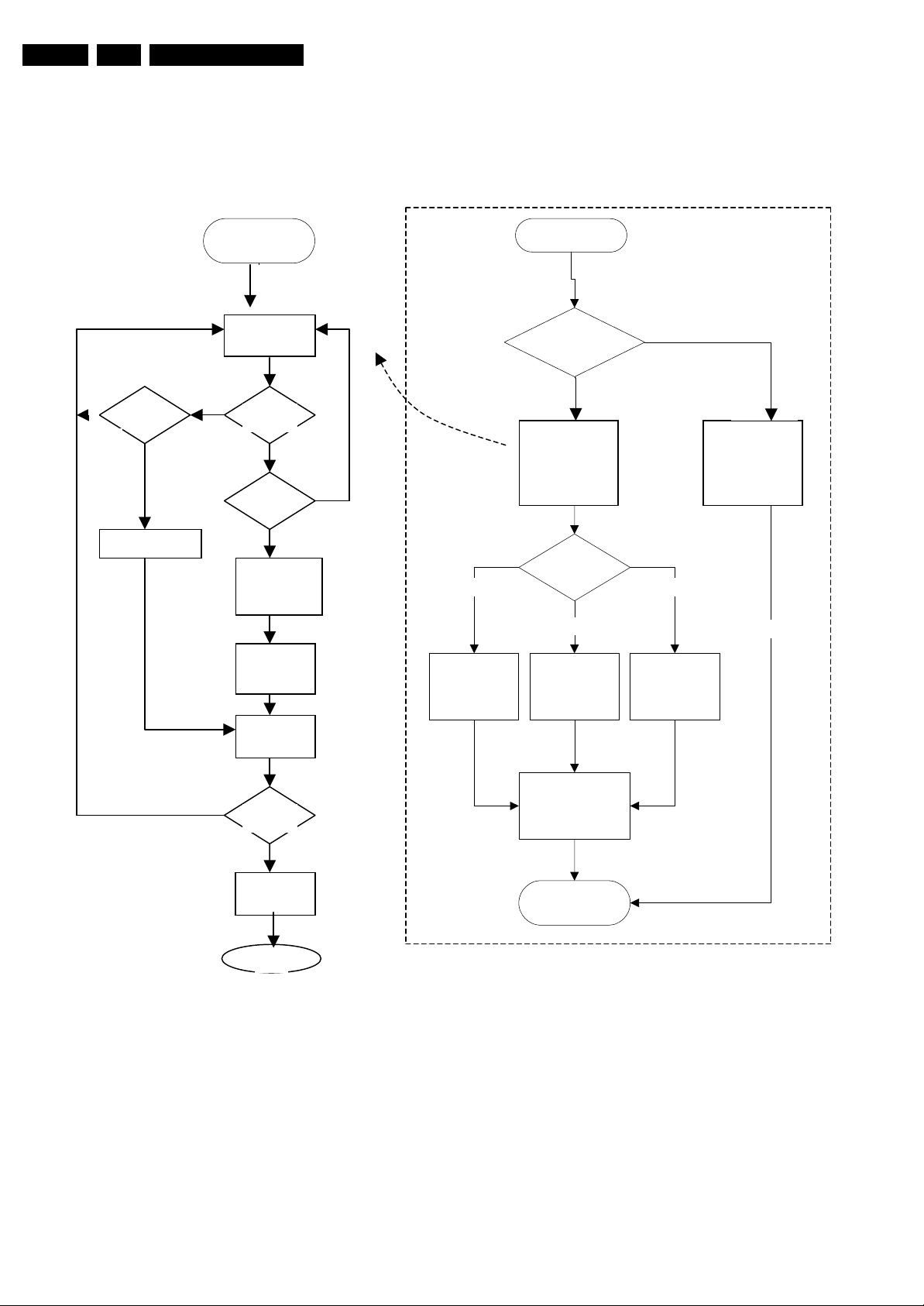
5.3 Stepwise Start-up
The stepwise start-up method, as known from FTL/FTP sets is
not valid any more. The situation for this chassis is as follows:
Power Management
Power On Command Sequence
start
SSB
12V turn on
yes
EBJ initialize
13 sec to com
Video blank and
Power time
audio mu
35 sec?
no
(max.
plete).
te
out
12V to MCU
Send
message
when the TV is in a protection state detected via the Stand-by
Processor (and thus blinking an error) and SDM is activated via
shortcutting the pins on the SSB, the TV starts up until it
reaches the situation just before protection. So, this is a kind of
automatic stepwise start-up. In combination with the start-up
diagrams below, you can see which supplies are present at a
certain moment.
Important to know here is, that if e.g. the 3V3 detection fails
(and thus error 11 is blinking) and the TV is restarted via SDM,
the Stand-by Processor will enable the 3V3, but will not go to
protection now. The TV will stay in this situation until it is reset
(Mains/AC Power supply interrupted).
The abbreviations “SP” and “MP” in the figures stand for:
• SP: protection or error detected by the Stand-by
Processor.
• MP: protection or error detected by the VIPER Main
Processor.
MTV 512 MCU
MCU initialize
(minimum 15sec
to com
lete
MCU send “initialize complete”
to SSB.
Note: This message shall be sent
at 1 sec interval till SSB Ack
for a
eriod of 10 sec
Fatal Comm
Error -
ShutDown
comm to mcu and
Stop chking “I am
.
yes
CCA
Mode
SSB suspend
maintain 12V.
alive” msg
Check
message
MCU init
com
lete
Check m
ode
timeout 2 sec?
no
Check
mode
Normal
Mode
Send cca table and
video mute off to
MCU
End
No
messa
No
messa
ISP mode
SSB suspend
comm to mcu and
maintain 12V. Stop
chking “I am alive”
msg
MCU check mode send “Mode”
message to SSB.
Note: This message shall be sent at
0.2 sec interval till SSB Ack for
Send
messa
e
CCA Mode Normal mode
Set UART
MUX procedure
aperiodof1sec
MCU send “I
am alive”
messa
e
End
ISP mode
Set UART
MUX procedure
SSB and MTV512 MCU will execute the initialization
procedure upon receiving 12V. A buffer of 10 sec is
catered where “initialize complete” message is sent every
second for 10 times to ensure that SSB will receive this
message even in the situa tion of MTV512 MCU complete
initialization earlier than SSB.
G_15870_048.eps
120706
Figure 5-4 Power management - Power on
Page 20
EN 20 CT2.0U RA5.
p
Service Modes, Error Codes, and Fault Finding
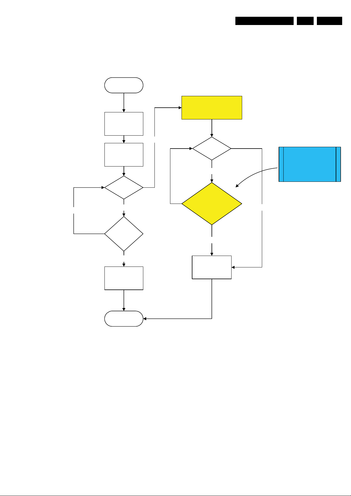
Abnormal State Detection
The MTV512 MCU shall turn-off OE system when any abnormal state occurs. Triggering of the state is
shown
Time out?
no
Set time out error
no
yes
Host(running time)
Check “I am alive”
message
Check “I am
alive” msg
“I am alive”
no
Error” msg to MCU,
MCU, TV5ceed
Host check whicnormal
Error exceptocess ion pr
state be triggered and execute
message
message
receive?
critical?
Received abnormal
message from MCU
TV510 send “Get
and upog
“Erro
to error exception
appropriate procedure
yes
yes
Error
present ?
yes
n receivin
SSB send
r” data from
“
get error” msg
10 pro
to
MCU
MCU return
error to
h one ab
SSB
SSB store
error in error
buffer
no
Lamp fail
Turn on lamp
LED
MCU (running time)
Abnormal detection
yes
Found abnormal state
Send “I am
alive” msg to
Send abnormal
SSB,
message to host
indicating
critical error
Check state
Thermal too high
Turn on thermal
LED
MTV 512 MCU
no
Send “I am
alive” msg to
SSB ,
indicating no
error
Fan rotation to low
normal
Turn on thermal
& lamp LED
simultaneously
no
n
Error
critical ?
yes
Error
end
exception
rocess
end
Shut down OE
system
end
G_15870_049.eps
110706
Figure 5-5 Power management - Error detected
Page 21
Service Modes, Error Codes, and Fault Finding
Power Off Command Sequence
The power-off sequence is as follows:
Start
Host get power-off
command
SSB mute
TV510 mute video
video and audio
on
10 SEC count
down done?
Other keys or no key press
no
YES
Host sends Power down mode
enter”“ to MCU
60 sec count
down done?
no
Chk ‘Power down mode
exit’ or “I am alive
command”command ?
EN 21CT2.0U RA 5.
MCU send message
“I am alive” or “power-
down mode exit”msg to host
After 60 sec
Key press?
Have warm-up key
SSB unmute and
run wake-up
procedure
end
Figure 5-6 Power management - Power off
5.4 Service Tools
5.4.1 ComPair
Introduction
ComPair (Computer Aided Repair) is a service tool for Philips
Consumer Electronics products. ComPair is a further
development on the European DST (service remote control),
which allows faster and more accurate diagnostics. ComPair
has three big advantages:
1. ComPair helps you to quickly get an understanding on how
to repair the chassis in a short time by guiding you
systematically through the repair procedures.
2. ComPair allows very detailed diagnostics (on I
is therefore capable of accurately indicating problem areas.
You do not have to know anything about I
yourself because ComPair takes care of this.
3. ComPair speeds up the repair time since it can
automatically communicate with the chassis (when the
microprocessor is working) and all repair information is
directly available. When ComPair is installed together with
2
C level) and
2
C commands
Received command
Host Power-off 12v
the Force/SearchMan electronic manual of the defective
chassis, schematics and PWBs are only a mouse click
away.
Specifications
ComPair consists of a Windows based fault finding program
and an interface box between PC and the (defective) product.
The ComPair interface box is connected to the PC via a serial
(or RS-232) cable.
For this chassis, the ComPair interface box and the TV
communicate via a bi-directional service cable via the service
connector(s).
The ComPair fault finding program is able to determine the
problem of the defective television. ComPair can gather
diagnostic information in two ways:
• Automatically (by communicating with the television):
ComPair can automatically read out the contents of the
entire error buffer. Diagnosis is done on I
ComPair can access the I
ComPair can send and receive I
2
C/UART bus of the television.
2
C/UART commands to
G_15870_050.eps
110706
2
C/UART level.
Page 22
EN 22 CT2.0U RA5.
Service Modes, Error Codes, and Fault Finding
the microcontroller of the television. In this way, it is
possible for ComPair to communicate (read and write) to
devices on the I
2
C/UART buses of the TV-set.
• Manually (by asking questions to you): Automatic
diagnosis is only possible if the microcontroller of the
television is working correctly and only to a certain extent.
When this is not the case, ComPair will guide you through
the fault finding tree by asking you questions (e.g. Does the
screen give a picture? Click on the correct answer: YES /
NO) and showing you examples (e.g. Measure test-point I7
and click on the correct oscillogram you see on the
oscilloscope). You can answer by clicking on a link (e.g.
text or a waveform picture) that will bring you to the next
step in the fault finding process.
By a combination of automatic diagnostics and an interactive
question / answer procedure, ComPair will enable you to find
most problems in a fast and effective way.
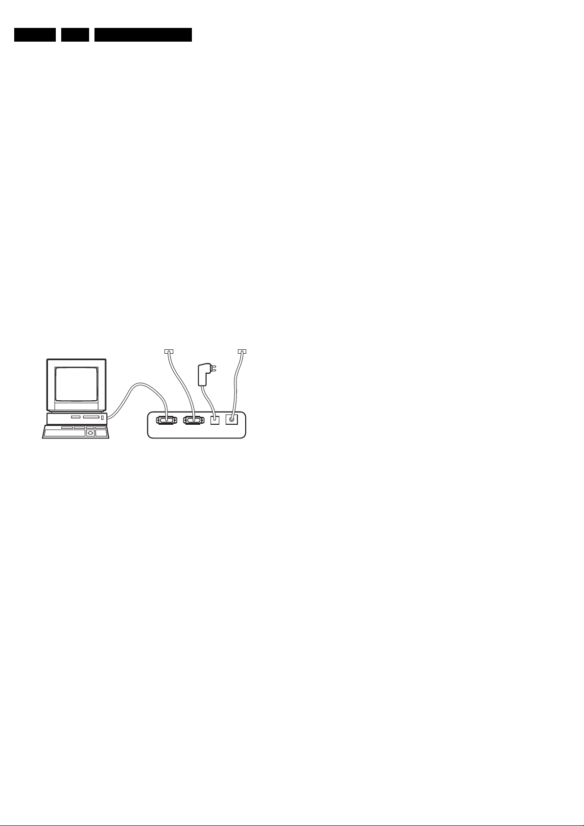
How to Connect
This is described in the chassis fault finding database in
ComPair.
Caution: It is compulsory to connect the TV to the PC as
shown in the picture below (with the ComPair interface in
between), as the ComPair interface acts as a level shifter. If
one connects the TV directly to the PC (via UART), ICs will be
blown!
TO
UART SERVICE
CONNECTOR
TO
I2C SERVICE
CONNECTOR
When multiple errors occur (errors occurred within a short time
span), there is a high probability that there is some relation
between them.
Basically there are three kinds of errors:
• Errors detected by the Stand-by Processor. These
errors will always lead to protection and an automatic start
of the blinking LED for the concerned error (see paragraph
“The Blinking LED Procedure”). In these cases SDM can
be used to start up (see chapter “Stepwise Start-up”).
• Errors detected by VIPER that lead to protection. In this
case the TV will go to protection and the front LED will blink
at 3 Hz. Further diagnosis via service modes is not possible
here (see also paragraph “Error Codes” -> “Error Buffer” > “Extra Info”).
• Errors detected by VIPER that do not lead to
protection. In this case the error can be read out via
ComPair, via blinking LED method, or in case you have
picture, via SAM.
5.5.2 How to Read the Error Buffer
Use one of the following methods:
• On screen via the SAM (only if you have a picture). E.g.:
– 00 00 00 00 00: No errors detected
– 06 00 00 00 00: Error code 6 is the last and only
detected error
– 09 06 00 00 00: Error code 6 was first detected and
error code 9 is the last detected error
• Via the blinking LED procedure (when you have no
picture). See next paragraph.
•Via ComPair.
PC VCR I2CPowe r
Figure 5-7 ComPair interface connection
How to Order
ComPair order codes:
• ComPair Software: ST4191.
• ComPair Interface Box: 4822 727 21631.
• AC Adapter: T405-ND.
• ComPair Quick Start Guide: ST4190.
• ComPair interface extension cable: 3139 131 03791.
• ComPair UART interface cable: 3122 785 90630.
Note: If you encounter any problems, contact your local
support desk.
5.5 Error Codes
5.5.1 Introduction
The error code buffer contains all detected errors since the last
time the buffer was erased. The buffer is written from left to
right, new errors are logged at the left side, and all other errors
shift one position to the right.
When an error has occurred, the error is added to the list of
errors, provided the list is not full or the error is a protection
error.
When an error occurs and the error buffer is full, then the new
error is not added, and the error buffer stays intact (history is
maintained), except when the error is a protection error.
To prevent that an occasional error stays in the list forever, the
error is removed from the list after 50+ operation hours.
9V DC
E_06532_021.eps
180804
5.5.3 How to Clear the Error Buffer
Use one of the following methods:
• By activation of the “RESET ERROR BUFFER” command
in the SAM menu.
• With a normal RC, key in sequence “MUTE” followed by
“062599” and “OK”.
• If the content of the error buffer has not changed for 50+
hours, it resets automatically.
5.5.4 Error Buffer
In case of non-intermittent faults, clear the error buffer before
you begin the repair (before clearing the buffer, write down the
content, as this history can give you significant information).
This to ensure that old error codes are no longer present.
If possible, check the entire contents of the error buffer. In
some situations, an error code is only the result of another error
code and not the actual cause (e.g., a fault in the protection
detection circuitry can also lead to a protection).
There are several mechanisms of error detection:
• Via error bits in the status registers of ICs.
• Via polling on I/O pins going to the stand-by processor.
• Via sensing of analogue values on the stand-by processor.
• Via a “not acknowledge” of an I
2
C communication
Take notice that some errors need more than 90 seconds
before they start blinking. So in case of problems wait 2
minutes from start-up onwards, and then check if the front LED
is blinking.
Page 23
Service Modes, Error Codes, and Fault Finding
Table 5-2 Error code overview
Error Description Error/Prot Detected by Device Defective module Result
3I2C3 P Stby µP n.a. I2C3_blocked Protection + Error blinking
5 VIPER does not boot (hardware failure) P Stby µP PNX8550 Protection + Error blinking
6 5V supply P Stby µP n.a. Control Protection + Error blinking
8 1.2V DC/DC P Stby µP n.a. Protection + Error blinking
11 3.3V DC/DC P Stby µP n.a. Protection + Error blinking
12 12V supply P Stby µP n.a. Protection + Error blinking
14 Class D amplifiers P Stby µP Class D Supply Protection + Error blinking
17 MPIF1 Audio Supply (ASUP) E VIPER KN10241C IF I/O Error logged
18 MPIF1 ref freq (ROK) E VIPER KN10241C IF I/O Error 32, 31, 18, 17, and 16 logged
25 Supply fault P Stby µP DC/DC Supply Protection + Error blinking
27 Phoenix E VIPER PNX2015B HD subsystem No error logged
29 AVIP1 E VIPER PNX3000 AV input processor 1 Errors 29, 32, 31, 18, 17, and 16 logged
32 MPIF1 E VIPER KN10241C Analog Front End 1 Errors 32, 18, 17, and 16 logged
34 Tuner1 E VIPER Tuner 1 No picture, error logged
37 Channel decoder E VIPER NXT2003 Channel decoder 1 Errors 34 and 37 logged
43 Hi Rate Front End E VIPER TDA8751 HDMI Error logged
44 Main NVM P VIPER M24C32 NVM Error logged + Error blinking 3 times
53 VIPER - HW peripheral problem P Stby µP PNX8550 Control Protection + Error blinking
65 GdeInitCommunicationFailure P PTV GDE / HCS Protection + Error blinking
67 System Integrity Failure E PTV GDE HCS Error logged
71 Overheating E CDE / HCS MTV512 CDE Lamp off, right red LED on, Errors 67 and 71 logged
72 Fan speed too low E CDE / HCS MTV512 CDE Lamp off, left + right red LED on, Errors 67 and 72 logged
73 Lamp broken E CDE / HCS MTV512 CDE Lamp off, left red LED on, Errors 67 and 73 logged
74 MCU initialisation failure E CDE / HCS MTV512 CDE
EN 23CT2.0U RA 5.
Extra Info
• Error 1 (I
2
C bus 1 blocked). When this error occurs, the TV
will go to protection and the front LED will blink at 3 Hz.
Now you can partially restart the TV via the SDM shortcut
pins on the SSB. Depending on the software version it is
possible that no further diagnose (error code read-out) is
possible. With the knowledge that only errors 1, 2, 4, and
63 result in a 3 Hz blinking LED, the range of possible
defects is limited.
• Error 2 (I
2
C bus 2 blocked). When this error occurs, the
TV will go to protection and the front LED will blink at 3 Hz.
Now you can partially restart the TV via the SDM shortcut
pins on the SSB. Due to hardware restriction (I
the fast I
2
C bus) it will be impossible to start up the VIPER
2
C bus 2 is
and therefore it is also impossible to read out the error
codes via ComPair or via the blinking LED method. With
the knowledge that only errors 1, 2, 4, and 63 result in a 3
Hz blinking LED, the range of possible defects is limited.
When you have restarted the TV via the SDM shortcut pins,
and then pressed "CH+" on your remote control, the TV will
go to protection again, and the front LED blink at 3 Hz
again. This could be an indication that the problem is
related to error 2.
• Error 3 (I
on I
2
C bus 3 blocked). There are only three devices
2
C bus 3: VIPER, Stand-by Processor, and NVM. The
Stand-by Processor is the detection device of this error, so
this error will only occur if the VIPER or the NVM is blocking
the bus. This error will also be logged when the NVM gives
no acknowledge on the I
2
C bus (see error 44). Note that if
the 12 V supply is missing (connector 1M46 on the SSB),
the DC/DC supply on the SSB will not work. Therefore the
VIPER will not get supplies and could block I
a missing 12 V can also lead to an error 3.
• Error 4 (I
• Error 5 (I
severe hardware problem around the VIPER (supplies not
OK, VIPER completely dead, I
2
C bus 4 blocked). Same remark as with error 1.
2
C bus 5 blocked). This error will point to a
2
C link between VIPER and
2
C bus 3. So,
Stand-by Processor broken, etc...).
• Error 7 (8.6 V error). Except a physical problem with the
8.6 V itself, it is also possible that there is something wrong
with the Audio DC Protection: see paragraph "Hardware
Protections" for this.
• Error 12 (12 V error). Except a physical problem with the
12 V itself, it is also possible that there is something wrong
with the Audio DC Protection: see paragraph "Hardware
Protections" for this.
• Error 14 (Audio supply). This error is triggered in case of
too low voltage of the audio supplies and therefore a drop
of the audio supply voltage of below approx. 9 V per supply
rail (or lower than 18 V rail to rail). Also a DC voltage of
higher than 1 V DC on the speakers will lead to protection
and error 14 blinking. For LCD sets this circuit can be found
on schematic SA3, for PDP sets this can be found on
schematic C. It should be noted that for 26-inch models
there is only a supply link between the amplifiers and the
stand-by µC whereas in all other models this link is
implemented by Audio-Prot line pin 7 on 1 M02.
• Error 29 (AVIP1). This error will probably generate extra
errors. You will probably also see errors 32 (MPIF) and
error 31 (AVIP 2). Error 29 and 31 will always be logged
together due to the fact that both AVIPs are inside the
PNX2015 and are on the same I
2
C bus. In this case start
looking for the cause around AVIP (part of PNX2015).
• Error 31 (AVIP2). See info on error 29.
• Error 34 (Tuner 1). When this error is logged, it is not sure
that there is something wrong with the tuner itself. It is also
possible that there is something wrong with the
communication between channel decoder and tuner. See
schematic B2B.
• Error 37 (Channel decoder). This error will always log
error 34 (tuner) extra. This is due to the fact that the tuner
2
I
C bus is coming from the channel decoder.
• Error 44 (NVM). This error will never occur because it is
masked by error 3 (I
for error 3 checks on an I
2
C bus 3). The detection mechanism
2
C acknowledge of the NVM. If
NVM gives no acknowledge, the stand-by software
assumes that the bus is blocked, the TV goes to protection
and error 3 will be blinking.
• Error 53. This error will indicate that the VIPER has started
to function (by reading his boot script, if this would have
failed, error 5 would blink) but initialization was never
completed because of hardware peripheral problems
(NAND flash, ...) or software initialization problems.
Possible cause could be that there is no valid software
loaded (try to upgrade to the latest main software version).
5.6 The Blinking LED Procedure
5.6.1 Introduction
The blinking LED procedure can be split up into two situations:
Page 24

EN 24 CT2.0U RA5.
Service Modes, Error Codes, and Fault Finding
• Blinking LED procedure in case of a protection detected by
the stand-by processor. In this case the error is
automatically blinked. This will be only one error, namely
the one that is causing the protection. Therefore, you do
not have to do anything special, just read out the blinks. A
long blink indicates the decimal digit, a short blink indicates
the units.
• Blinking LED procedure in the “on” state. Via this
procedure, you can make the contents of the error buffer
visible via the front LED. This is especially useful for fault
finding, when there is no picture.
When the blinking LED procedure is activated in the “on” state,
the front LED will show (blink) the contents of the error-buffer.
Error-codes > 10 are shown as follows:
1. “n” long blinks (where “n” = 1 - 9) indicating decimal digit,
2. A pause of 1.5 s,
3. “n” short blinks (where “n”= 1 - 9),
4. A pause of approx. 3 s.
5. When all the error-codes are displayed, the sequence
finishes with a LED blink of 3 s,
6. The sequence starts again.
Example: Error 12 9 6 0 0.
After activation of the SDM, the front LED will show:
1. 1 long blink of 750 ms (which is an indication of the decimal
digit) followed by a pause of 1.5 s,
2. 2 short blinks of 250 ms followed by a pause of 3 s,
3. 9 short blinks followed by a pause of 3 s,
4. 6 short blinks followed by a pause of 3 s,
5. 1 long blink of 3 s to finish the sequence,
6. The sequence starts again.
Protections during Start-up
During TV start-up, some voltages and IC observers are
actively monitored to be able to optimize the start-up speed,
and to assure good operation of all components. If these
monitors do not respond in a defined way, this indicates a
malfunction of the system and leads to a protection. As the
observers are only used during start-up, they are described in
the start-up flow in detail (see paragraph “Stepwise Start-up").
5.7.2 Hardware Protections
There is one hardware protection in this chassis: “Audio DC
Protection”. This protection occurs when there is a DC voltage
on the speakers. In that case the main supply is switched "off",
but the stand-by supply is still working.
For the Samsung V4 PDP displays, the 8V6 supply is switched
"off" and the LED on the display’s Main Supply blinks eleven
times, which means there is an overvoltage protection. The
front LED of the TV will blink error 7 (8V6 error).
In case of LCD supplies, the 12V supply will drop. This will be
detected by the stand-by processor, which will start blinking the
12 V error (error 12).
Repair Tip
• It is possible that you have an audio DC protection because
of an interruption in one or both speakers (the DC voltage
that is still on the circuit cannot disappear through the
speakers).
5.6.2 How to Activate
Use one of the following methods:
• Activate the SDM. The blinking front LED will show the
entire contents of the error buffer (this works in “normal
operation” mode).
• Transmit the commands “MUTE” - “062500” - “OK”
with a normal RC. The complete error buffer is shown.
Take notice that it takes some seconds before the blinking
LED starts.
•Transmit the commands “MUTE” - “06250x” - “OK”
with a normal RC (where “x” is a number between 1 and
5). When x= 1 the last detected error is shown, x= 2 the
second last error, etc.... Take notice that it takes some
seconds before the blinking LED starts.
5.7 Protections
5.7.1 Software Protections
Most of the protections and errors use either the stand-by
microprocessor or the VIPER controller as detection device.
Since in these cases, checking of observers, polling of ADCs,
filtering of input values are all heavily software based, these
protections are referred to as software protections.
There are several types of software related protections, solving
a variety of fault conditions:
• Protections related to supplies: check of the 12V, +5V,
+8V6, +1.2V, +2.5V and +3.3V.
• Protections related to breakdown of the safety check
mechanism. E.g. since a lot of protection detections are
done by means of the VIPER, failing of the VIPER
communication will have to initiate a protection mode since
safety cannot be guaranteed anymore.
Remark on the Supply Errors
The detection of a supply dip or supply loss during the normal
playing of the set does not lead to a protection, but to a cold
reboot of the set.
Page 25

Service Modes, Error Codes, and Fault Finding
EN 25CT2.0U RA 5.
5.8 Fault Finding and Repair Tips
Read also paragraph "Error Codes" - "Extra Info".
5.8.1 Exit “Factory Mode”
When an "F" is displayed in the screen's right corner, this
means that the set is in "Factory" mode, and it normally
happens after a new SSB has been mounted.
To exit this mode, push the "VOLUME minus" button on the
TV's keyboard control for 5 seconds and restart the set
5.8.2 MPIF
Important things to make the MPIF work:
• Supply.
• Clock signal from the AVIP.
2
•I
C from the VIPER.
5.8.3 AVIP
Important things to make the AVIP work:
• Supplies.
• Clock signal from the VIPER.
2
•I
C from the VIPER (error 29 and 31).
5.8.4 DC/DC Converter
Introduction
• The best way to find a failure in the DC/DC converters is to
check their starting-up sequence at power "on" via the
Mains/AC Power cord, presuming that the Stand-by
Processor is operational.
• If the input voltage of the DC/DC converters is around 12 V
(measured on the decoupling capacitors 2U17/2U25/
2U45) and the ENABLE signals are "low" (active), then the
output voltages should have their normal values.
• First, the Stand-by Processor activates the +1V2 supply
(via ENABLE-1V2).
• Then, after this voltage becomes present and is detected
OK (about 100 ms), the other two voltages (+2V5 and
+3V3) will be activated (via ENABLE-3V3).
• The current consumption of controller IC 7U00 is around 20
mA (that means around 200 mV drop voltage across
resistor 3U22).
• The current capability of DC/DC converters is quite high
(short-circuit current is 7 to 10 A), therefore if there is a
linear integrated stabilizer that, for example delivers 1.8V
from +3V3 with its output overloaded, the +3V3 stays
usually at its normal value even though the consumption
from +3V3 increases significantly.
• The +2V5 supply voltage is obtained via a linear stabilizer
made with discrete components that can deliver a lot of
current. Therefore, in case +2V5 (or +2V5D) is shortcircuited to GND, the +3V3 will not have the normal value
but much less.
• The supply voltage +12VSW is protected for over-currents
by fuse 1U04.
• Symptom: +1V2 present for about 100 ms. Supplies +2V5
and +3V3 not rising.
1. Check the ENABLE-3V3 signal (active "low").
2. Check the voltage on pin 8 (1.5 V).
3. Check the under-voltage detection circuit (the voltage
on collector of transistor 7U10-1 should be less than
0.8 V).
4. Check for output voltages short-circuits to GND (+3V3,
+2V5 and +2V5D) that generate pulsed over-currents
of 7-10 A through coil 5U00.
5. Check the over-current detection circuit (2U18 or 3U83
interrupted).
• Symptom: +1V2 OK, but +2V5 and +3V3 present for about
100 ms. Cause: The SUPPLY-FAULT line stays "low"
even though the +3V3 and +1V2 is available. The Stand-by
Processor is detecting that and switches all supply
voltages "off".
1. Check the drop voltage across resistor 3U22 (this
could be too high)
2. Check if the +1V2 or +3V3 are higher than their normal
values. This can be due to defective DC feedback of
the respective DC/DC converter (3U18 or 3UA7).
• Symptom: +1V2, +2V5, and +3V3 look okay, except the
ripple voltage is increased (audible noise can come from
the filtering coils 5U00 or 5U03).
Cause: Instability of the frequency and/or duty cycle of one
or both DC/DC converters.
– Check resistor 3U06, the decoupling capacitors, the
AC feedback circuits (2U20 + 2U21 + 3U14 + 3U15 for
+1V2 or 2U19 + 2U85 + 3U12 + 3U13 for +3V3), the
compensation capacitors 2U09, 2U10, 2U23 and
2U73, and IC 7U00.
Note 1: If fuse 1U01 is broken, this usually means a pair of
defective power MOSFETs (7U01 or 7U03). Item 7U00 should
be replaced as well in this case.
Fault Finding
• Symptom: +1V2, +2V5, and +3V3 not present (even for a
short while ~10ms).
1. Check 12V availability (fuse 1U01, resistor 3U22,
power MOS-FETs) and enable signal ENABLE-1V2
(active low).
2. Check the voltage on pin 9 (1.5 V).
3. Check for +1V2 output voltage short-circuit to GND that
can generate pulsed over-currents 7-10 A through coil
5U03.
4. Check the over-current detection circuit (2U12 or 3U97
interrupted).
Page 26
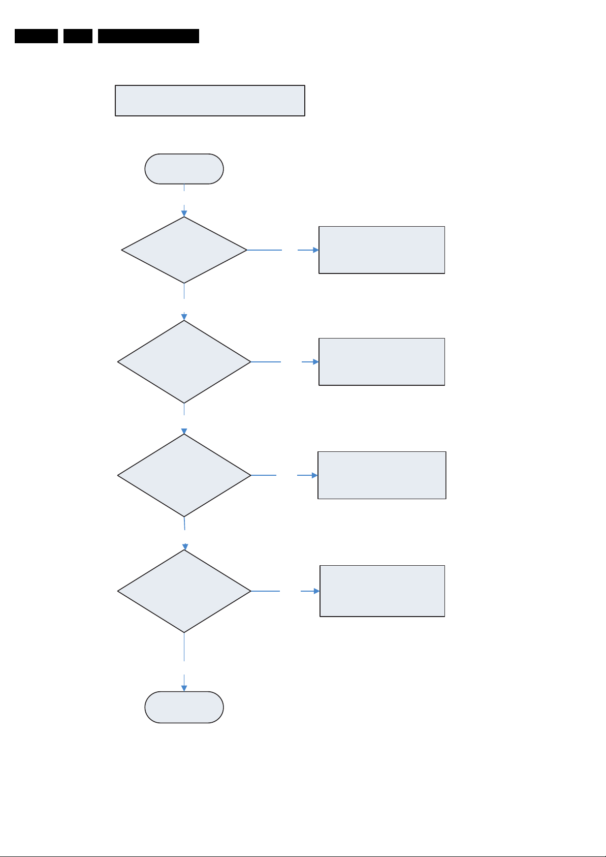
EN 26 CT2.0U RA5.
5.8.5 Flowcharts
Service Modes, Error Codes, and Fault Finding
Troubleshooting Flow
Start
YES
Is Power LED
Solid Green ?
YES
Image Problem
NO
Audio Problem
NO
YES
YES
A. Power
Troubleshooting
B. Image Performance
Troubleshooting
C. Sound
Troubleshooting
NO
Remote control
Problem
NO
End
YES
Figure 5-8 Troubleshooting flow
D. Remote
Troubleshooting
G_15870_051.eps
100706
Page 27
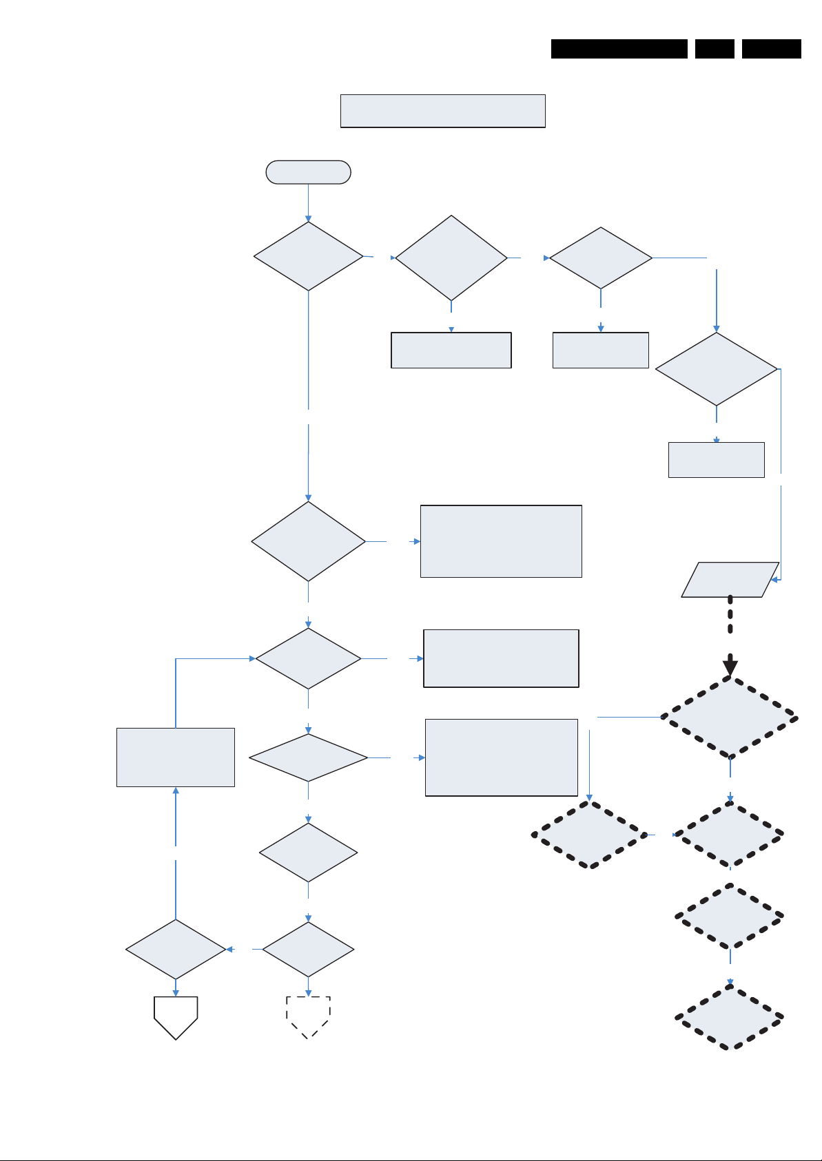
Service Modes, Error Codes, and Fault Finding
A . Power Troubleshooting -1
Start
EN 27CT2.0U RA 5.
Is Power LED
lit ?
YES
Power LED RED
/ Green Twinkle ?
NO
Power LED
Green Twinkle ?
NO
Power cord or
Input Voltage ok ?
Supply AC Power or
change Power Cord
It is 1st step Power OFF state,
YES
It is Warming Up state , please
YES
YES
NO
Push Power button to return
TV Normal state
wait 10 sec for lamp on time
Power SW
turned on ?
NO
Turn on Power
Switch
YES
Check Lamp Door
assemble properly
NO
Reassemble Lamp
Door
No Power
issue
Repair Center
YES
Push Power button to
enter Warming Up
state
Temp LED lit ?NONO
B A
NO
RED Twinkle ? YES
NO
Power LED
solid RED
YES
Lamp LED
lit ?
Figure 5-9 Troubleshooting A - Power 1/2
It is 2nd step Power Off
state , Please wait 40 sec for
cooling time , then turn on
Power button .
Change Inter-
NO
Lock
Check Inter-Lock
Change LVPS
NO
Change Keypad
switch ok ?
YES
Board
NO
Change Main
Board
NO
G_15870_052.eps
100706
Page 28
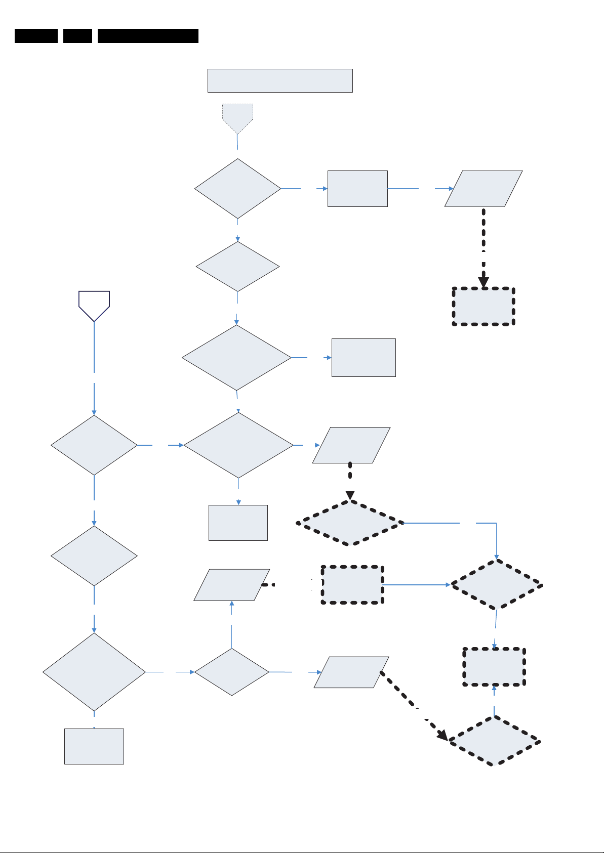
EN 28 CT2.0U RA5.
Service Modes, Error Codes, and Fault Finding
A. Power Troubleshooting -2
A
YES
B
YES
Temp LED solid
RED ?
YES
Lamp LED solid
RED ?
NO
Lamp LED RED
twinkle ?
YES
Check environment temp.
over 70 degree ?
NO
Check the ventilation
openings on TV block ?
YES Change Lamp YES
YES
NO
Move out the
high temp. source
Temp
Issue
Lamp
Issue
Repair Center
Change Ballast
Board
NO
Temp LED RED
twinkle
YES
Check the ventilation
openings on TV
block ?
YES
Move block out
NO
YES
Move block out
Temp
Issue
NO
Is system Fan
spin ?
Repair Center
YES
Repair Center
Check System Fan
spin ?
Change System
Fan
Temp
Issue
Repair Center
YES
Check Engine Fan
spin ?
NO
Change Engine
Fan
NO
Check Engine Fan
spin ?
G_15870_053.eps
100706
Figure 5-10 Troubleshooting A - Power 2/2
Page 29
Service Modes, Error Codes, and Fault Finding
B. Image Performance Troubleshooting
EN 29CT2.0U RA 5.
Start
Fuzzy image
Start
Image no
Display
Connecting OK ?
YES
Connection correct?
YES
Is the Device operate
correct ?
NO
NO
NO
Reconnect your
connection
Change to correct
position
Change to Correct
operate state
Change to correct setting NO
Change to correct setting NO
YES
Is source correct?
YES
Is TV source setting math
real connection ?
YES
Is OSD setting
Correct ?
YES
No Image or
Fuzzy Image
Issue
NO
Change to Correct
Repair
Center
Source
Change Engine
NO
Change Main Board
NO
Is Video input from
AV 7 ?
Change Keypad
YES
NO
Board
G_15870_054.eps
100706
Figure 5-11 Troubleshooting B - Image Performance
Page 30
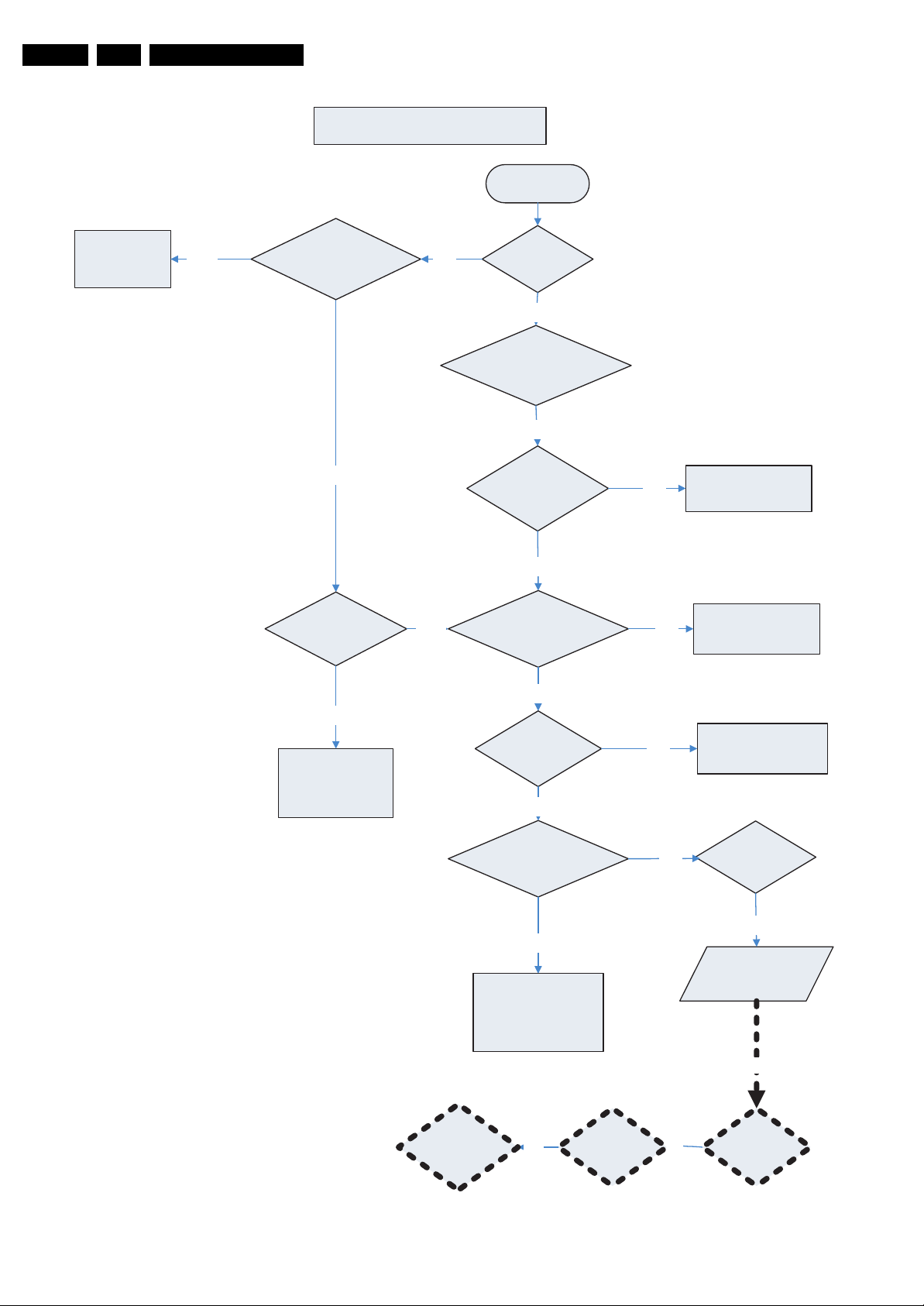
EN 30 CT2.0U RA5.
Service Modes, Error Codes, and Fault Finding
C. Sound Trouble Shooting
Start
Disconnect
earphone
YES
Does earphone
connect ?
NO
Is connection
ok ?
NO
Reconnect your
connection
YES
NO
Does Sound
with noise ?
Is connection
Is the Device operate
Can hear
Sound ?
YES
YES
correct ?
YES
correct ?
YES
Is source
correct ?
YES
NO
NO
Change to Correct
NO
Correct your
connection
operate state
Change to Correct
Source
The "Mute " function
is on ?
YES
Close the " Mute "
function
Change Keypad
Board
Figure 5-12 Troubleshooting C - Sound
Change
Amplifier
Board
NO
NONO
Volume
setting OK ?
YES
No Sound
Issue
Repair Center
Change
speaker
G_15870_055.eps
100706
Page 31

Service Modes, Error Codes, and Fault Finding
D . Remote Control Trouble Shooting
Start
EN 31CT2.0U RA 5.
Distance from TV to
Remote over 8 meter ?
NO
Angel from Remote to
TV over 30 degree
NO
Battery
ok ?
YES
Remote control
not working Issue
NO
YES
YES
Shorten the
distance
Correct the remote
angel to TV
Replace new Battery and
put correct position
Repair Center
Change Remote
Control
NO
Change Keypad
Board
NO
Change Main
Board
G_15870_056.eps
100706
Figure 5-13 Troubleshooting D - Remote Control
Page 32

EN 32 CT2.0U RA5.
Service Modes, Error Codes, and Fault Finding
5.9 Software Upgrading
5.9.1 Introduction
The set software and security keys are stored in a NAND-Flash
(item 7P80), which is connected to the VIPER via the PCI bus.
It is possible for the user to upgrade the main software via the
USB port. This allows replacement of a software image in a
standalone set, without the need of an E-JTAG debugger. A
description on how to upgrade the main software can be found
in the "Directions For Use".
Important: When the NAND-Flash must be replaced, a new
SSB must be ordered, due to the presence of the security
keys!!! See table “SSB service kits” for the order codes.
Perform the following actions after SSB replacement:
1. Set the correct option codes (see sticker inside the TV).
2. Update the TV software (see chapter 3 for instructions).
3. Perform the alignments as described in chapter 8.
4. Check in CSM menu 5 if the HDMI and POD keys are valid.
Table 5-3 Service kit (CT2.0U RA chassis)
Item 12NC
SSB
Note: After replacing the SSB, execute the alignments
according to the instructions in this manual.
5.9.2 Main Software Upgrade
The software image resides in the NAND-Flash, and is
formatted in the following way:
Partition 1
Trimedia2 image
Trimedia1 image
MIPS image
Partition 0
USB Download Application
uBTM (boot block)
Figure 5-14 NAND-Flash format
Executables are stored as files in a file system. The boot loader
(uBTM) will load the USB Download Application in partition 0
(USB drivers, bootscript, etc.). This application makes it then
possible to upgrade the main software via USB.
Installing "Partition 0" software is possible via an external
EJTAG tool, but also in a special way with the USB stick (see
description in paragraph “Partition 0“).
Partition 1 (Customer)
To do a main software upgrade (partition 1) via USB, the set
must be operational, and the "Partition 0" files for the VIPER
must be installed in the NAND-Flash!
The new software can be uploaded to the TV by using a
portable memory device or USB storage compliant devices
(e.g. USB memory stick). You can download the new software
from the Philips website to your PC.
Partition 0 (Service)
If the "Partition 0" software is corrupted, the software needs to
be re-installed.
3139 268 00761
USB CUSTOMER
USB SERVICE
EJTAG
E_14700_082.eps
120505
To upgrade this “USB download application” (partition 0 except
the bootblock), insert an USB stick with the correct software,
but press the “red” button on the remote control (in ”TV” mode)
when it is asked via the on screen text.
Caution:
• The USB download application will now erase both
partitions (except the boot block), so you need to reload the
main SW after upgrading the USB download application.
As long as this is not done, the USB download application
will start when the set is switched “on”.
• When something goes wrong during the progress of this
method (e.g. voltage dip or corrupted software file), the set
will not start up, and can only be recovered via the EJTAG
tool!
5.9.3 Manual Start of the Main Software Upgrade Application
Normally, the software upgrading procedure will start
automatically, when a memory device with the correct software
is inserted, but in case this does not work, it is possible to force
the TV into the software upgrade application. To do so:
• Disconnect the TV from the Mains/AC Power.
• Press the “OK” button on a Philips DVD RC-6 remote
control (it is also possible to use the TV remote in "DVD"
mode).
• Keep the “OK” button pressed while connecting the TV to
the Mains/AC Power.
• The software upgrade application will start.
• When a memory device with upgrade software is
connected, the upgrade process will start.
5.9.4 Stand-by Software Upgrade
It will be possible to upgrade the Stand-by software via a PC
and the ComPair interface. Check paragraph "ComPair" on
how to connect the interface. To upgrade the Stand-by
software, use the following steps:
1. Disconnect the TV from the Mains/AC Power.
2. Short circuit the SPI pins [2] on the SSB. They are located
outside the shielding (see figure “SDM and SPI service
pads” earlier in this chapter).
3. Keep the SPI pins shorted while connecting the TV to the
Mains/AC Power.
4. Release the short circuit after approx. two seconds.
5. Start up HyperTerminal (can be found in every Windows
application via Programs -> Accessories ->
Communications -> HyperTerminal. Use the following
settings:
–COM1
– Bits per second = 38400
– Data bits = 8
– Parity = none
– Stop bits = 1
– Flow control = Xon / Xoff.
6. Press “Shift U” on your PC keyboard. You should now see
the following info:
– PNX2015 Loader V1.0
– 19-09-2003
–DEVID=0x05
–Erasing
– MCSUM=0x0000
–=
7. If you do not see the above info, restart the above
procedure, and check your HyperTerminal settings and the
connections between PC and TV.
8. Via “Transfer” -> “Send text file ...”, you can send the
proper upgrade file to the TV. This file will be distributed via
the Service Organization.
9. After successful programming, you must see the following
info:
– DCSUM=0xECB3
–:Ok
– MCSUM=0xECB3
Page 33

Service Modes, Error Codes, and Fault Finding
– Programming
– PCSUM=0xECB3
– Finished
10. If you do not see this info, restart the complete procedure.
11. Close HyperTerminal.
12. Disconnect and connect Mains/AC Power again.
5.9.5 MTV512 Software Upgrade
Introduction
If necessary the MTV512 firmware can be upgraded. For that
purpose you need the newest firmware and some special
hardware.
At the time of writing, this information was not available.
This will be updated as soon as it is available.
EN 33CT2.0U RA 5.
Page 34

EN 34 CT2.0U RA5.
Personal Notes:
Service Modes, Error Codes, and Fault Finding
E_06532_012.eps
131004
Page 35

Block Diagrams, Test Point Overviews, and Waveforms
6. Block Diagrams, Test Point Overviews, and Waveforms
Wiring Diagram
35CT2.0U RA 6.
1
2
3
X100
4
POWER SUPPLY
SIDE I/O &
KEYPAD BOARD
J302
POWER SW
GND
10
GND
12
KEYBOARD
GND
14
1
GND
FRONT_Y_CVBS
3
5
GND
FRONT C
7
9
GND
11
AUDIO_IN5_L
2
GND
J301
AUDIO_IN5_R
13
GND8
HP_L
4
HP_R
6
15
USB
16
USB
USB
17
18
USB
1
2
3
1
2
3
4
5
6
1M361M60 1M01
7
8
9
10
11
1
2
3
4
6543211
LED2 1.48V
8910
CTRL_DISP1
CTRL_DISP2
CTRL_DISP3
CTRL_DISP4
TXPNXA+
TXPNXB+
1M21
RC 3.52V
LED1 0V
+5V2STBY
573
J1
POWER BUTTON
BOARD
VDISP
VDISP
VDISP
VDISP
NC
NC
GND
TXPNXA-
GND
TXPNXB-
GND
LAMP_LED
TEMP_LED
4
2
1
2
3
4
5
6
7
8
9
10
11
12
13
14
15
16
GND
6
GND
17
18
TXPNXC-
19
TXPNXC+
20
GND
21
TXPNXCLK-
22
TXPNXCLK+
23
GND
24
TXPNXD-
1G50
25
TXPNXD+
26
GND
27
TXPNXE-
28
TXPNXE+
29
GND
SCL-12C4
30
31
SDA-12C4
GND
32
6
5
243
1
J5 J1
9
2.9V
TXD
5
1
2
3
1740
4
8
3.3V
RXD
4
231
7
3.3V
0V
VSYNC
GND
213
J4
465
SSB
1D50
3
465
MTV512
X405X404
GND
GND
V9(12V)
V9(12V)
X
POWER IN
B
NC
HOT GND
X
X
B
R
O
BR
0V0V4.96V
4.78V
R
306V
Y
4.96V
X
PROJ
LAMP
+14.5V
-14.5V
V4+13V
V5-13V
2
1
+5V
+5V
+5V2
+5V2
V4V5GND
5
4
3
GND
6
1J02
GND
7
+12V
V2(12V)
GND
9
8
0.66V ON 5V OFF
+12V
PSON
V2(12V)
13
12
11
10
X406 X104
LIGHT
ENGINE
LV DS
1
2
+12V
1
2
3
GND
1
J2 J8
2
3
4
5
6
7
8
SDA_DMD
SCL_DMD
GND
GND
LAMPLITZ
RESETZ
GND
ASIC_READY
3.3V
3.3V
0V
0V
0V
3.29
0V
3.3V
X
VIDEO IN
X
CONTROL
R
Y
XXX X
B
DMD FANBALLAST FAN LAMP FAN
Y
B
Y
B
6.95V
0
0
7.16VR
0
0
6VR
0
0
DMD
FAN
LAMP
FAN
BALLAST
FAN
3.3V
3.3V
3.3V
SDA
SCL
GND
+3V3
X
TEMP SENSOR
BOARD
G_15870_002.eps
100706
Page 36

Block Diagrams, Test Point Overviews, and Waveforms
Block Diagram Video (SSB Only)
VIDEO
MAIN TUNER
B02B
1T04
TD1336O/FGHP
MAIN HYBRID
TUNER
CHANNNEL DECODER
B02A
7T22
NXT2004
DTV CABLE AND
TERRESTRIAL
RECEIVER
QAM 8VSB
Demodulator
FEC
Micro-
Controller
QPSK
Demodulator
MPEG_DATA
SIDE I/O
VIDEO
S VIDEO
ANALOG I/O
B07C
PR
PB
AV1
Y
VIDEO
IN
PR
PB
AV2
Y
VIDEO
IN
VIDEO
AV3
S VIDEO
12
IF-OUT
IF-1
15
IF-2
FM-T
13
IF-AGC
34
38
8
7
ADC
ADC
48
GPIO
84
ADC
29
30
DV1F-DATA(0-7)
J306
J305
1
3
5
4
2
1I04
1I03
1I00
1I01
1
3
5
4
2
1T01
14
1
14
SAW 44MHz
4
FAT-IF-AGC-MAIN
AUX-IF-AGC
FAT-ADC-INN
FAT-ADC-INP
FM-TRAP
IRQ-FE-MAIN
1T11
25M14
B05C
VIPER
SIDE_IO_Y_CVBS
SIDE_IO_C
IF-ANA
TO
7T13
LA7795T-E
2
7
8
3
in
AGC COTROL
AV7_Y-CVBS
AV1_CVBS
AV2_Y-CVBS
AV2_ C
PR1
PB1
7
6
out
7T12
B05A
Y1
PR
PB
Y
B07b
B07b
B07b
B03a
B07b
B07b
B07b
B03a
B03a
B03a
J301
N.C.
B07C
B07C
B07C
3
7
N.C.
N.C.
B07A
B07A
B07A
B07A
B07A
B07A
B07A
B07A
B03
IF-ANA
CVBSOUTIF-MAIN
1M36
2
4
B07A
HDMI
CONNECTOR
MPIF MAIN:
1A10
2
7A11
EF
4
AV1_CVBS
AV2_Y-CVBS
AV2_ C
AV7_Y-CVBS
FRONT_Y-CVBS
FRONT_C
HDMI +SUPPLY
1I06
1
3
4
6
1
7
9
10
12
18 2
15
19
16
19
1B02
7
8
5
ARX-HOTPLUG
3A17
ARX-DCC-SCL
ARX-DCC-SDA
7B20
H-SYNC-VGA
V-SYNC-VGA
7A00
PNX3000HL
B03C
VIFINP
107
108
VIFINN
SIFINP
99
SIFINN
100
CVBSOUTIF
120
B03A
SOURCE SELECTION
123
CVBS-IF
126
CVBS1
1
CVBS2
12
CVBS_DTV
CVBS|Y34
5
C3
8
CVBS|Y4
9
C4
15
Y_COMB
16
C_COMB
25
R|PR|V_1
26
G|Y|Y_1
27
B|PB|U_1
30
R|PR|V_2
31
G|Y|Y_2
32
B|PB|U_2
ARX2+
ARX2-
ARX1+
ARX1-
ARX0+
ARX0-
ARXC+
ARXC-
HPD-HIRATE
B05A
Y
Y1
PR
PR1
Y
Y1
PB
PB1
36CT2.0U RA 6.
PNX 2015:
B04
7J00
IF
SOUND
BPF
LPF
LC
TRAP
A
M
GROUP
DELAY
QSS
TO AM INTERNAL
LPF
P
QSSOUT
LPF
AUDIO SWITCH
LPF
CVBS/Y RIM
C-PRIM
B03B
SUPPLY
SUPPLY
DIGITAL
BLOCK
CVBS-OUTA
CVBS-OUTB
14
28
35
44
43
19
22
+5V
SCL-DMA
SDA-DMA
N.C.
N.C.
MPIF
60
+
YUV
RGB
CLAMP
HDMI: I/O + CONTROL
B07B
7B50
TDA9975HS
180
RX2+A
179
RX2-A
174
RX1+A
173
RX1-A
168
RX0+A
167
RX0-A
162
RXC+A
161
RXC-1
RX2+B
RX2-B
RX1+B
RX2-B
RX0+B
RX0-B
RXC+B
RXC-B
HSCL B
HSDA B
131
HSYNC
128
VSYNC
90
88
G/Y
96
R/PR
94
81
G/Y
79
68
B/PB
66
CVBS SEC
LEVEL
ADAPT
INV.
PAL
Termination
resistance
control
Termination
resistance
control
Line time
measuremebt
Activity
detection &
sync selec.
Slicers
ADC
CLAMP
LPF
Yyuv
U
V
MONO SEC.
receiver
A
D
2nd
SIF
A/D
A
A
CLP PRIM
CLP SEC
CLP yuv
HDMI
HDMI
Sync
seperator
Clocks
generator
Yyuv
2FH
A
D
Yyuv
2Fh
D
D
Upsample
Derepeater
HDCP
STROBE1N
DATA
STROBE1P
LINK
DATA1N
1
DATA1P
STROBE3N
STROBE3P
DATA
LINK
DATA3N
3
DATA3P
STROBE2N
STROBE2P
U,V
DATA
LINK
DATA2N
2
DATA2P
TIMING
CIRCUIT
Video
output
formatter
2
VHREF
1
timing
201
generator
207
142
I2C slave
143
interface
STROBE1N-MAIN
STROBE1P-MAIN
61
62
63
50
51
52
53
55
56
57
123
46
40
DATA1N-MAIN
DATA1P-MAIN
STROBE3N-MAIN
STROBE3P-MAIN
DATA3N-MAIN
DATA3P-MAIN
STROBE2N-MAIN
STROBE2P-MAIN
DATA2N-MAIN
DATA2P-MAIN
HV-PRM-MAIN
N.C.
AV6_VSYNC
N.C.
DV4-DATA(0-7)
DV5-DATA(0-7)
DV4- CLK
DV-HREF
DV-VREF
DV-FREF
SDA-MM
SCL-MM
PNX 2015: STANDBY
B04E
& CONTROL
7LA7
M25P05
512K
FLASH
CLK-MPIF
AV2_FBL
SPI-SDO
5
SPI-CLK
6
SPI-CSB
1
SPI-WP
3
1LA0
16M
PNX2015E
B04C
B04A
R4
AVP1_DLK1SN
R3
AVP1_DLK1SP
R2
AVP1_DLK1DN
R1
AVP1_DLK1DP
N4
AVP1_DLK3SN
N3
AVP1_DLK3SP
N2
AVP1_DLK3DN
N1
AVP1_DLK3DP
P4
AVP1_DLK2SN
P3
AVP1_DLK2SP
P2
AVP1_DLK2DN
P1
AVP1_DLK2DP
M3
AVP1_HVINFO1
M4
MPIF_CLK
L2
AVP2_HSYNCFBL2
G2
AVP2_VSYNC2
B04B
DV4_DATA_0 T0 9
DV5_DATA_0 T0 9
AK8
AH9
DV-HREF
AJ9
DV-VREF
AK9
DV-FREF
B4E
STANDBY
AK10
AH10
AG10
PROCESSOR
AJ27
AJ12
AH12
TUNNELBUS
AUDIO/VIDEO
DV I/O INTERFACE
STANDBY
See
Block digram
Control
DATA LINK 1
DATA LINK 3
DATA LINK 2
AVIP-1
AVIP-2
North tunnel
Memory
based scaler
Video MPEG
decoder
VIP
PNX2015
COLUMBUS
3D Comb
filter and
noice
reduction
B04D
DDR INTERFACE
VO-2
MUX
VO-1
LVDS_TX
Memory
controller
South tunnel
DV2_CLK
DV3_CLK
DV1_DATA(0-9)
DV2_DATA(0-9)
DV3_DATA(0-9)
RGB_HSYNC
RGB_VSYNC
RGB_CLK_IN
RGB_UD
RGB_DE
RIN (0-9)
GIN (0-9)
BIN (0-9)
LVDS_AN
LVDS_AP
LVDS_BN
LVDS_BP
LVDS_CN
LVDS_CP
LVDS_CLKN
LVDS_CLKP
LVDS_DN
LVDS_DP
LVDS_EN
LVDS_EP
PMX-MA(0-12)
PNX-MDATA
(0-15)
MCLK_P
MCLK_N
TUN-VIPER-RX-DATA
TUN-VIPER-TX-DATA
TUN-VIPER-RX-CLKP
TUN-VIPER-TX-CLKN
TUN-VIPER-TX-CLKP
DV2A-CLK
AF30
DV3F-CLK
AK28
From
B02A
CHANNEL
DECODER
DV1F-DATA(0-7)
DV3F-DATA (0-7)
J29
J28
J30
J27
K26
B26
C26
A25
B25
D25
E25
C23
D23
B24
C24
E24
F24
PMX-MA
PNX-MDATA
PNX-MCLK-P
A17
PNX-MCLK-N
A16
B05
MP-OUT-HS
MP-OUT-VS
MP-CLKOUT
MP-OUT-FFIELD
MP-OUT-DE
AH19
AG25
VIPER:
7V00
PNX8550
TUNNELBUS
7L50
K4D261638F
45
46
B05C B05B
MAIN MEMORY
VIPER
Tunnel
B05C
AUDIO/VIDEO
2-Layer
secondary
video out
Dual SD
single HD
MPE2 decoder
250Mhz
MIPS32
CPU
Scaler and
de-interlacer
1SD+1HD
YUV
Video in
Video
TS
router
Dual
con
acces
F28
F27
E30
DV-CLKIN
DV-OUT-HS
DV-OUT-VS
TXPNXA-
TXPNXA+
TXPNXB-
TXPNXB+
TXPNXC-
TXPNXC+
TXPNXCLK-
TXPNXCLK+
TXPNXD-
TXPNXD+
TXPNXE-
TXPNXE+
DDR
SDRAM
128Mx16
Temporal
noise redux
B05A
CONTROL
G26
DV-OUT-FFIELD
DV-ROUT(0-9)MP-ROUT(0-9)
DV-GOUT(0-9)MP-GOUT(0-9)
DV-BOUT(0-9)MP-BOUT(0-9)
Memory
controller
2D DE
5 Layer
primary
video out
HD/VGA/
E29
DV-OUT-DE
DVD
CSS
MM_DATA
MM_A(0-12)
C4
1H00
A2
27M
DV-RO UT
DV-GOUT
656
DV-BOUT
VIPER/PNX 2015:
B04G
DISPLAY INTERFACE
VDISP
5J50
5J52
5J54
5J56
5J58
5J60
SCL-I2C4
SDA-I2C4
VIPER: MAIN MEMORY
B05B
7V01
K4D551638F
SDRAM 1
7V02
K4D551638F
SDRAM 2
VIDEO-DAC
B06
1G50
1
2
3
4
12
13
15
16
18
TO VIDEO IN
19
LIGHT ENGINE
21
22
24
25
27
28
30
31
DDR
8Mx16
DDR
8Mx16
G_15870_003.eps
070706
Page 37

Block Diagrams, Test Point Overviews, and Waveforms
Block Diagram Audio (SSB Only)
AUDIO
MAIN TUNER
B02B
1T04
B02A
AUDIO IN
L+R
B07C
AV1
AUDIO IN
L+R
AV2
AUDIO IN
L+R
AV3
AUDIO IN
L+R
AV3
DIGITAL
AUDI O
OUT
TD1336O/FGHP
HYBRID TUNER
7T22
NXT2004
CABLE AND
TERRESTRIAL
RECEIVER
SIDE I/O
J306
ANALOG I/O
1I04
1I03
1I00
1I00-1
MAIN
DTV
12
FOR MORE MORE DETAILS
SEE ALSO BLOCK DIAGRAM
VIDEO AND CONTROL
DV1F-DATA(0-7)
SIDE_IO_L
SIDE_IO_R
AUDIO-IN4-R
AUDIO-IN4-L
AUDIO-IN1-R
AUDIO-IN1-L
AUDIO-IN2-R
AUDIO-IN2-L
SPDIF-OUT1
IF-ANA
J301
11
13
B03d
B03d
B03d
B03d
B03d
B03d
B03
1M36
6
8
B07c
B07c
B07c
B07c
B07c
B07c
B3f
B3f
MPIF MAIN:
1A10
2
AUDIO-IN5-L
AUDIO-IN5-R
AUDIO-IN1-R
AUDIO-IN1-L
AUDIO-IN2-R
AUDIO-IN2-L
AUDIO-IN4-L
AUDIO-IN4-R
AUDIO-OUT1-R
AUDIO-OUT1-L
37CT2.0U RA 6.
PNX2015
7A00
PNX3000HL
IF
B03C
VIFINP
107
7
108
VIFINN
8
99
100
128
127
85
86
83
84
80
79
70
69
BLOCKDIAGRAM
SIFINP
SIFINN
AUDIO SOURCE
B03D
SELECTIOM
AUDIO SWITCH
LPF
AUDIO SWITCH
(DIGITAL OUT)
L5
R5
R1
L1
R2
L2
L4
R4
LINE / SCART L/R
SEE ALSO
VIDEO
A
D
AM SOUND
B05
AB29
MPIF
DLINK1
DLINK2
AUDIO SWITCH
(ANALOG OUT)
VIPER:
7V00
PNX8552EH
B5C
SPDIF-OUT1
AUDI O
AMPS
VIPER
DATA LINK
72
73
74
DSND
75
40
I2S_IN1_WS
I2S_IN1_SCK
I2S_OUT2_SD0
I2S_OUT2_SD1
I2S_OUT2_SD2
I2S_OUT1_SD0
I2S_OUT2_SD3
DATA LINK 1
DATA LINK 2
DATA LINK 3
DSNDR2
DSNDL2
DSNDR1
DSNDL1
CLK-MPIF
T29
T30
T28
T27
R30
U27
R29
I2S-WS-MAIN
I2S-BCLK-MAIN
I2S-MCH-LR
I2S-MCH-CSW
I2S-MCH-SLR
I2S-SUB-D
I2S-MAIN-D
B04
AC3
AD3
AE3
AF3
M4
V3
V2
U2
U3
U4
V5
V4
7J00
PNX2015E
I2D
ADCAC12
ADCAC11
ADCAC10
ADCAC19
I2S
OUT
I2S
IN
PNX2015
PNX2015: AUDIO/VIDEO
B04A
DEM DEC
AVIP
ADAC1
AUDIO
PROCESSING
ADAC2
ADAC7
ADAC8
AH1
AG1
AB1
AA1
AUDIO: AMPLIFIER
B08A
7D10-02
ADAC1
7D10-3
ADAC2
FEEDBACK
INV-MUTE
MUTE
MPIF MAIN: AUDIO AMPLIFIER
B03E
7A04-1
ADAC7
7A04-2
ADAC8
A-PLOP
MUTE
INV-MUTE
7D26
CONTROL
7D14÷7D16
CONTROL
FEEDBACK-LR
FEEDBACK-RL
7D19÷7D22
CONTROL
CONTROL
AUDIO-HDPH-L-AP
AUDIO-HDPH-R-AP
+12_20V
7D18
7D18
-12_20V
+12_20V
7D23
7D23
-12_20V
7D10-1
7D10-4
U-VOLT-DETECT
LEFT-SPEAKER
7D11
PROT-AUDIOSUPPLY
CONTROL
RIGHT-SPEAKER
SOUND-ENABLE
7D25
CONTROL
MPIF MAIN: VIDEO SOURS
B03A
SELECTION
AUDIO-HDPH-L-AP
AUDIO-HDPH-R-AP
B05A
N.C.
B04E
1M36
10
11
7
AUDIO: CONNECTORS
B08B
LEFT-SPEAKER
RIGHT-SPEAKER
-12-16V-NF
B01B
+12-16V-NF
B01B
+12_20V
SIDE I/O
J301
4
6
2
-12_20V
PROT-AUDIOSUPPLY
HEAD_PHONE_L
HEAD_PHONE_R
HP_DETECT
5M02
5M03
5M10
5M12
JP301
2
3
4
5M11
5M09
1740
1M02
RES
1
2
3
4
1
2
3
4
5
6
7
Speaker L
15W/8Ω
Speaker R
15W/8Ω
Headphone
Out 3.5mm
VIPER: MAIN MEMORY
B05B
7V02
7V01
HDMI +SUPPLY
B07A
1I06
1
2
18
19
HDMI
CONNECTOR
K4D551638F
2X DDR
SDRAM
8Mx16
ARX2+
AUDI O
MULTIPLEXED
WITH VIDEO
SEE ALSO
BLOCKDIAGRAM
VIDEO
MM_DATA
MM_A(0-12)
MAIN MEMORY
B05B
HDMI: I/O + CONTROL
B07B
7B50
TDA9970HS
RX2+
RX2-
RX1+
Termination
RX1-
Resistance
RX0+
RX0-
RXC+
RXC-
DDR
INTERFACE
HDMI PANELLINK
RECEIVER
Control
HDMI
receiver
Audio PLL
HDCP
Formatter
Audio FIFO
extraction
Audio
Packet
AA27
183
SPDIF-HDMI
SPDIF-HDMI
DV4-DATA
DV5-DATA
DV
INPUT
G_15870_004.eps
070706
Page 38

Block Diagrams, Test Point Overviews, and Waveforms
Control & Clock Signals (SSB Only)
CONTROL + CLOCK SIGNALS
J301
17 1
16 2
18 3
15
B05
DV 1F - DATA
1M60
4
B02A
CHANNEL DECODER
7T22
NXT2004
30
CABLE AND
TERRESTRIAL
4321
25M14
29
J307
CHANNEL +
CHANNEL -
VOLUM E +
VOLUM E -
RECEIVER
1
2
3
4
MENU
POWER
1T11
D
SIDE I/O
USB 1.1
CONNECTOR
KEYPAD BOARD
POWER BUTTON BOARD
DTV
L302
L301
51
84
59
D5,D6
D7,D8
D11,D12
IRQ-FE-MAIN
USB1.1_DM
USB1.1_DP
VIPER:
RESET-FE-MAIN
USB-BUS-PW
PWR_LED
DV1F-CLK
IRQ-MAIN
USB1-DM
USB1-DP
KEY_SEL
KEY_SEL
D10
AH16
AH27
1H00
7V00
PNX8550EH/M1/S1
B05C
B05A
A26
F1
AJ29
AJ28
C4
27M
A2
B05B
J301
22
J302
1
J1
8
96
5
A/V + TUNNELBUS
VIPER
CONTROL
MAIN MEMORY
B05F
MISCELLANEOUS
1M01
1M21
4
LED1
LED2
E30
AH19
AG25
K3
T2
T1
AG22
AB28
AK12
AJ12
AK5
AJ7
AA2
W2
D28
AD2
AD27
C27
AB27
D29
B5
C30
AD3
AD4
B28
A18
B18
DV-CLKIN
TUN-VIPER-TX-CLKN
TUN-VIPER-TX-CLKP
CHDEC-CLK
NAND
NAND-CLE
NAND-ALE
NAND-REn
NAND-WEn
NAND-SEL
PLL-OUT
PCI-CLK-VPR
HPD-HIRATE
SOUND-ENABLE
HDMI-COAST
M135-CLK
POWERDOWN-HDMI
M27-PNX
RESET-MIPS
DEBUG-BREAK
MM_CLK_N
MM_CLK_P
KEYBOARD
3H06
B07A
B08A
B04A
PNX2015:
DV2A-CLK
DV3F-CLK
TUN-VIPER-RX-CLKP
B05E
VIPER: EEPROM
7P80
TC58DVM92F1
EEPROM
(32Mx16)
16
17
8
18
9
19
STBY-WP-NAND-FLASH
B07B
HDMI: I/O + CONTROL
7B50
TDA9975HS/8/C1
124
HDMI
135
CONTROL
115
RESET-SYSTEM
B05B
VIPER: MAIN MEMORY
7V01
46
7V02
B04E
B01A
B01A
B07A
B08A
45
DDR
SDRAM
16Mx16
DETECT-1V2 (P2.0)
DETECT-3V3 (P2.2)
DETECT-8V6 (P2.4)
POWER-OK-DISPLAY
PROT-AUDIOSUPPLY (P2.7)
LED1
LED2
38CT2.0U RA 6.
DV4-CLK
2
DETECT-5V (P2.3)
DETECT-12V (P2.5)
SUPPLY-FAULT
DEBUG-BREAK
P50-HDMI
KEYBOARD
B04E
AF30
AK28
M29
U30
U28
AK8
Y28
AG19
AJ21
AG21
AF16
AH17
AG17
AK18
AJ18
AH14
AG13
AG21
AG13
AG18
AK23
AK21
AG20
7J00
PNX2015E
DV I/O INTERFACE
B04B
PNX2015
TUNNELBUS
B04C
DDR INTERFACE
B04D
DV I/O INTERFACE
B04B
STANDBY + CONTROL
B04E
J30
M4
A16
A17
AH10
AJ27
AH20
AJ12
1LA0
AH12
STBY-WP-NAND-FLASH
AG22
AH15
AK16
AJ21
AH21
AH22
BACKLIGHT-CONTROL
AJ16
AJ16
AG16
MP-CLKOUT
CLK-MPIF
PNX-MCLK-N
PNX-MCLK-P
SPI-CLK
SPI-WP
SDM
16M
ENABLE-1V2 (P0.2)
ENABLE-3V3 (P0.4)
RESET-SYSTEM
RESET-AUDIO
RESET-MAIN-NVM
LAMP-ON (P0.5)
UART-SWITCH (P0.7)
9P24
9P14
SDM
B05E
B01A
B05A
B04A
B05E
B04G
B16A
B10D
B06
DISPLAY INTERFACE: MOP
7G00
XC3S200-4TQG144C
DV-CLKIN
MP-CLK
B03B
MPIF MAIN: SUPPLY
24
7A00
PNX3000HL/N3
40
CONTROL
B04D
PNX 2015: DDR INTERFACE
7L50
K4D261638F
46
SDRAM
45
128Mx16
B04E
PNX 2015: STANDBY & CONTROL
7LA7
M25P05-AVMN6P
6
3
MOP
MPIF
E/W &
DDR
512K
FLASH
D2
IR
RECEIVER
IRRCVR0
3
3
1
1
LIGHT-SENSOR
RC
LIGHT-SENSOR
RC
AK13
AH23
AJ16
AA27
RESET-PNX2015
G_15870_005.eps
070706
Page 39

I2C (SSB Only)
I²C
VIPER: CONTROL
B5A
Block Diagrams, Test Point Overviews, and Waveforms
+3V3
B7A
HDMI + SUPPLY
HDMI: I/O + CONTROL
B7B
39CT2.0U RA 6.
SUPPLY + RS232
B1B
I2C1-SDA
I2C1-SCL
7V00-5
SM PNX8552EH
VIPER
PROT
PROT
05
53
I2C2-SDA
I2C2-SCL
A25
C25
F26
E27
B27
D25
A29
A28
C2
AD4
AF29
AD26
3Q11
SDA-MM
3Q10
SCL-MM
TXD-VIPER
RXD-VIPER
EJTAG-TDI
EJTAG-TDO
EJTAG-TMS
EJTAG-TCK
JTAG-TRST
RESET-SYSTEM
3Q13
SDA-DMA
3Q12
SCL-DMA
VIPER: MAIN MEMORY
B5B
3H23
3H22
B01B
+3V3
3H05
3H04
7V01
K4D551638F
DDR
SDRAM 1
7V02
K4D551638F
DDR
SDRAM 2
1
18 2
19
2x HDMI
CONNECTOR
MPIF MAIN: SUPPLY
B3B
1I06
16
15
3B08
5 6
7B02
M24C02
EEPROM
3A14
3A15
43 44
7A00-3
PNX3000HL
MPIF
ERR
ERR
18
32
ARX-DDC-SDA
ARX-DDC-SCL
3B07
SDA-MM
SCL-MM
3Q11
PARX-DDC-SDA
3Q10
PARX-DDC-SCL
PNX 2015: STANDBY & CONTROL
B4E
3LF8
3LG9
AF9
AG9
ERR
45
JTAG-TRST
3LH3
3LH4
G4
G5
7J00-6
PNX2015E
CONTROL
AVI PCOLUMBUS HD
ERR
ERR
ERR
31
29
29
145
146
107
3LH1
3B61
142 143
7B50-1
TDA9970HS
HDMI
CONTROL
ERR
43
3LH0
B27
ERR
27
3B60
C27
SDA-DMA
SCL-DMA
AF11
AF21
AJ21
7L50
K4D261638F
JTAG-TRST
EJTAG-DETECT
RESET-SYSTEM
DDR
SDRAM
16Mx16
B5A
CHANNEL DECODER
B2A
9T11
9T12
9U07
RES
7T23
PCA9515ADP
2
3
9T10
9T13
RES
3T53
6
7
JTAG-TRST
EJTAG-DETECT
EJTAG-TDI
EJTAG-TDO
EJTAG-TMS
EJTAG-TCK
RESET-SYSTEM
+3V3
3T54
3T52
3T51
43
42
RECEIVER
1H07
1
2
3
5
7
9
11
I2C-SDA-TUNER
I2C-SCL-TUNER
90
91
7T22
NXT2004
DTV
ERR
37
EJTAG
CONNECTOR
(FACTORY USE
ONLY)
B2B
MAIN TUNER
+5VTUN
3T28
3T25
3T22
3T23
9 8
1T04
TD1336/FGHP
MAIN
DIG TUNER
ERR
34
I2C3-SDA
I2C3-SCL
UA1_TX
UA1_RX
I2C4-SDA
I2C4-SCL
AE27
AG29
E24
B26
A3
B4
3Q15
3Q14
3H99
3H98
SDA-I2C4
SCL-I2C4
B5E
SDA-UP-VIP
SCL-UP-VIP
VIPER: EEPROM
7P80
TC58DVM92F1TGI0
EEPROM
32Mx16
+3V3
3Q03
3Q04
PROT
03
RESET-MAIN-NVM
7P18
VIPER/PNX 2015:
B4G
DISPLAY INTERFACE
GLINK-TXD
GLINK-RXD
8
1D50
5 6
7P14
M24C64
EEPROM
MAIN
NVM
8
TO J1
MTV512
9
BOARD
+3V3-STANDBY
3LE3
3LE4
TXD-UP
RXD-UP
B05E
7LA7
M25P05-AVMN6P
DDR
SDRAM
16Mx16
3LJ1
3LJ0
AJ19
AK19
3LF0
AG26 AH26
7J00-5
PNX2015E
PNX2015
STANDBY
3LE2
AG16
AF14
AG14
3LM7
+3V3-STANDBY
3LH8
SCL-UP-SW
3LH9
SCL-UP-SW
UART-SWITCH
3LC7
3LC6
B5E
VIPER: EEPROM
B5A
B4E
B4E
B5A
7P16
TXD-VIPER
TXD-UP
RXD-UP
RXD-VIPER
UART-SWITCHn
7P17
7P15
74HC4066PW
10
9
2
3
5
12
6
13
UART
B7D
8
11
1
4
TXD
RXD
3I10
3I11
CONNECTOR
1M16
1
3
2
COMPAIR
SERVICE
(UART)
PROT
04
G_15870_006.eps
070706
Page 40

Block Diagrams, Test Point Overviews, and Waveforms
Supply Lines Overview (SSB Only)
40CT2.0U RA 6.
SUPPLY LINES OVERVIEW
POWER SUPPLY
A
-SUPPLY_AUDIO
+SUPPLY_AUDIO
+12V
+5V
STANDBY
SUPPLY + RS232
B01B
X404
11
22
66
77
78
99
10 10
44
55
66
11 11
12 12
13 13
B01b
B01a
B01a
B01a
B01a
B01b
B01a
1J02
STANDBY
BACKLIGHT-CNTRL-OUT
LAMP-ON-OUT
B01a
DC / DC
B01A
+12VS
1U01
5U02
7U00
Control
CHANNEL DECODER
B02A
+2V5
+3V3
+1V2 +1V2
7T20
+3V3
+12VSW +12VSW
+5V +5V
MAIN TUNER
B02B
+12SW
5U37
5U38
5U35
5U36
1
16
7T21
CONTROL
7U01
7U03
7U27
+2V5
STABILIZER
5T20
5T21
5T23
5T24
5T25
5T26
5T27
7T10
IN OUT
COM
5U00
5U03
5T28
5T11
7U25
7U24
POD-MODE
7U28
-12-16V-NF
+12-16V-NF
+12VS
+5V2-STBY
+5V
+12VSW
+12VS
+12VSW
+3V3
B02a,B04a,e,f,g,
+1V2
+2V5
+2V5D
+2V5
+2V5D-PLL
+2V5A-PLL
+2V5A
+2V5A-XTAL
+2V5A-ADC
+2V5F
+3V3
+3V3F
+1V2_ATSC
+1V2F
+12SW
+5VTUN
B05a,c,d,e,B06
B07a,b
B08B
B08B
B01a
B03e,B04a,
B05e,f
B02a,
B03a,b,c,e,
B04e,g,B05a,
B06,B07a
B01b
B01b
B01b
B02b
B02b
B03e
B01b
B01b
B01a
B03b
B01a
B01a
B01b
B01a
B03b
B01a
B01a
B01a
B01a
B05f
B01a
B05f
B01b
B01a
B02a,
B04g,B07c
B01b,B02b,
B03e,B04e,
B02a,
B04a,d,e,f,
B04c,f,B05d
B02a,B04e
B03c,d
MPIF MAIN: VIDEO SOURCE SELECTOIN
B03A
+5V +5V
MPIF MAIN: SUPPLY
B03B
+5V +5V
5A12
7A00
2
MPIF
MPIF MAIN: IF + SAW FILTER
B03C
+5V +5V
5A16
+5VTUN
5A17
MPIF MAIN: AUDIO SOURCE SELECTION
B03D
+5VTUN
+8V-AUD
MPIF MAIN: AUDIO AMPLIFIER
B03E
+5V
+5V2-STBY
+12VSW
7A17
7A05
VREF-AUD
PNX2015: AUDIO / VIDEO
B04A
+1V2
+3V3
+5V2-STBY
+12VSW
VREF-AUD-POS
PNX2015: TUNNELBUS
B04C
+2V5 +2V5
3L38
PNX2015: DDR INTERFACE
B04D
+1V2
+2V5
5L52
5L51
PNX2015: STANDBY & CONTROL
B04E
+1V2
+1V2-STANDBY
+3V3
+3V3-STANDBY
+5V
+12VSW
3L20
7A10
3L21
VREF-AUD-POS
VREF-AUD
+5V2-STBY
VREF-AUD
+5V2-STBY
VREF-AUD-POS
VREF-PNX
+2V5-DDRPNX
VREF-DDRPNX
+1V2-STANDBY
+3V3-STANDBY
+5VaM
+5VTUN
+5VbM
+5VTUN
+8V-AUD
+5V
+12VSW
+8V-AUD
+1V2
+3V3
+12VSW
+1V2
+2V5
+1V2
+3V3
+5V
+12VSW
B01a
B01a
B05f
B05f
B01a
B04d
B01a
B05f
B01b
B01a
B01a
B01b
B05d
B01a
B04c
B01a
B01a
B01a
B01a
B05f
B01b
B01b
PNX2015: SUPPLY
B04F
+1V2 +1V2
5LN1
+3V3 +3V3
+1V2-STANDBY +1V2-STANDBY
B04a
+3V3-STANDBY +3V3-STANDBY
B03e
+2V5 +2V5
+2V5-DDRPNX +2V5-DDRPNX
B04G
+3V3 +3V3
+3V3-STANDBY +3V3-STANDBY
+5V
+12VSW +12VSW
+3V3
B05A
+3V3 +3V3
+5V +5V
B03d
B05B
+2V5-VPR +2V5-VPR
B05C
+3V3 +3V3
VREF-PNX VREF-PNX
B05D
+1V2 +1V2
+2V5 +2V5
B05c
+3V3 +3V3
B05E
+3V3 +3V3
+3V3-STANDBY +3V3-STANDBY
B04f
+5V2-STBY +5V2-STBY
B05F
+5V2-STBY
5LN3
5LN0
5LN2
PNX2015: DISPLAY INTERFACE
7J04
7J08
7J07
CONTROL
VIPER: CONTROL
VIPER: MAIN MEMORY
3H52
3H50
VIPER: A/V + TUNNELBUS
VIPER: SUPPLY
5Q07
VIPER: EEPROM
MISCELLANEOUS
7M05
IN OUT
COM
7M06
IN OUT
COM
5J11
5M00
PLL-1V2
LVDS-3V3
PLL-3V3
UP-3V3
+5V
VDISP
VREFD-VPRDDR
VREF-VPRDDR
+2V5-VPR
+5V2-STBY
+3V3-STANDBY
+1V2-STANDBY
1M21
VIDEO-DAC
B06
B01a
B01b
B01a
B01b
B07a
B07a
B01a
B07a
B07a
B07a
B07a
B01a
B05f
B05f
B08b
B08b
B01b
B01b
5
+3V3 +3V3
5G10
+5V +5V
7G42
IN OUT
COM
HDMI + SUPPLY
B07A
+3V3 +3V3
5B17
5B11
5B12
7B25
IN OUT
COM
+5V
7B45
IN OUT
COM
1I06
HDMI
CONNECTOR
B07B
+1V8 +1V8
+1V8-PLL +1V8-PLL
+3V3 +3V3
+3V3-DIG +3V3-DIG
+3V3-AVI +3V3-AVI
+3V3-PLL +3V3-PLL
+3V3-APLL +3V3-APLL
B07C
+12VSW +12VSW
B07D
+3V3-STANDBY +3V3-STANDBY
B08A
+3V3-STANDBY +3V3
+12_20V +12_20V
-12_20V -12_20V
B05b
B08B
-12-16V-NF -12-16V-NF
+12-16V-NF +12-16V-NF
1M02
1
2
3
N.C.
4
5
6
B07d,B08a
B04e,f,g,
B05e
B04e,f
J1`
5
18
HDMI: I/O + CONTROL
ANALOG I/O
UART
AUDIO: AMPLIFIER
3D43
7D24
5D16
AUDIO: CONNECTORS
5M10
5M11
5M12
5M09
KEYBOARD
+5V2STBY +5V2STBY
5B18
5B10
+3V3DAC
+3V3-APLL
3V3-PLL
3V3-DIG
+1V8
+1V8-PLL
+5V2-STBY
+3V3-AV
+3V3-AVI
AIN-5V
VP
VN
-12_20V
+12_20V
B07b
B07b
B07b
B07b
B07b
B07b
B08a
B08a
G_15870_007.eps
070706
Page 41

Circuit Diagrams and PWB Layouts
7. Circuit Diagrams and PWB Layouts
41CT2.0U RA 7.
SSB: DC / DC
FU01
IU01
ENABLE-3V3
IU55 D8
IU56 D10
IU57 D11
IU58 D10
IU59 D11
IU60 D8
IU61 G3
+12VSW
+12VS
+1V2
+3V3
+2V5
+2V5D
IU62 A3
IU63 A3
IU65 D5
IU66 D4
IU68 E4
IU78 B11
IU79 B12
IU28 E8
IU29 B6
IU30 B6
IU31 B6
IU32 B6
IU33 A4
IU36 B6
A3K
R
2
IU81
IU37 E5
IU40 D8
IU41 D8
IU42 A12
IU44 C7
IU45 C6
IU54 B8
1U01
420T3A
6.3V
2U86
330u
+2V5 STABILIZER
3UA4
1%
1K0
47R
3UA5
1u0
2U46
GND-SIGGND-SIG
4
3
2U16
GND-SIG
IU10
3U06
7U00
4
7
10
8
9
39K
1u0
BST
1
2
1
2
ROSC
5
3U21 B8
3U22 A5
3U23 A6
3U24 A6
3U25 B6
3U26 B6
3U27 B6
3U22
14
VCC
VFB
COMP
GND-SIG
3U29
IU65
3U30
IU37
6U11
10R
IU24
Φ
GATE
GATE
IS
GND
3
1K0
1K0
BZX384-C9V1
2U17
H1
L1
H2
L2
+1
-1
+2
-2
3U28 B6
3U29 D5
3U30 D5
3U31 D4
3U32 E4
3U33 E4
3U34 B4
22u
IU31
1
2
16
15
5
6
1213
11
IU13
IU18
IU32
3U24
10R
IU19
IU15
3U09
3K3
3U25
3U23
4R7
IU17
3U35 B4
3U37 G2
3U38 G2
3U54 D11
3U55 D10
3U56 D11
3U82 C7
2
2R2
3U27
IU16
3U07
6K8
IU25
2U12
7U01-1
IU23
10R
4
IU29
3U28
2R2
100n
78
SI4936ADY
1
2U31
3n3
7U01-2
3U26
4R7
SI4936ADY
IU14
2U18
3U10
1K0
IU36
3U83 C7
3U85 A3
3U86 A3
3U87 A2
3U88 A3
3U89 B2
3U93 D10
6
5
SI4936ADY
3
IU30
7U03-1
2
3U08
3K3
100n
IU45
3U97
3U94 D11
3U95 E11
3U96 C7
3U97 C6
3UA1 B12
3UA2 B11
3UA3 D12
3UA4 D14
3UA5 D13
3UA7 E11
3UA8 D8
3UA9 D8
5U00 A8
5U02 A11
5U03 C9
6U11 E5
6U12 A3
6U21 E8
6U22 D7
6U23 D8
6U25 D12
7U00 B5
7U01-1 A6
7U01-2 A6
7U03-1 B6
7U03-2 B7
7U05-1 C3
7U05-2 C4
7U07 E7
7U10-1 D4
7U10-2 D4
7U13-1 A3
7U13-2 A3
7U15-1 D10
7U15-2 D10
7U27 C13
7U28 D12
7U29-1 B12
7U29-2 B11
9U03 H14
FU01 A14
FU02 B4
FU03 A8
FU05 E13
FU06 C9
FU07 E12
FU08 D12
FU13 C7
FU18 F12
FU19 F12
FU23 A4
IU01 A14
IU03 B3
IU04 B4
IU05 B4
IU06 B4
IU07 B4
IU08 C4
IU09 C4
IU10 C5
IU11 C3
IU12 C2
IU13 D6
IU14 C6
IU15 C6
IU16 B6
IU17 B6
IU18 A6
IU19 A6
IU20 A2
IU21 B8
IU22 B8
IU23 A6
IU24 A5
IU25 C6
IU26 D7
IU27 E7
8 9 10 11 12 13 14 15
7U29-1
BC857BS
100K
2U41
2
3
c111
2
7U28
PDZ9.1-B
6U25
1u0
IU42
1u0
1K0
2U58
3UA1
IU79
7U27
TS2431
IU80
2K2
3UA3
1
1
2U73
1n0
FU08
FU07
FU05
FU18
0V
2U25
5U02
10u
22u
IU86
12V/3.3V CONVERSION
FU03
10R
IU27
BAS316
BAS316
6U23
3UA8
68R
3UA9
68R
2U26
100n
3U11
220R
IU54
2U27
2U28
3U21
6U21
1n0
1n0
IU60
IU28
BZX384-C18
7U03-2
56
SI4936ADY
4
3
2U32
3n3
78
1
IU44
3U82
6K8
6K8
3U83
3U96
FU13
6K8
3K3
IU26
6U22
1u0
2U11
7U07
BC817-25W
BOOSTER
5U00
10u
2U19
IU22
3U13
IU21
3U12
100n
6K8
1K0
2U85
3n3
12V/1.2V CONVERSION
5U03
10u
10R
100n
2U20
IU40
3U14
3U15
3U16
2U21
6K8
1K0
4K7
IU55
3U20
2U29
2U30
1n0
IU41
1n0
GND-SIG
2U24
3n3
3U18
3U17
GND-SIG
22u1%
220R
1K0
1%
FU06
2U22
1
100n
2U72
4
7U29-2
BC857BS
22u
3U93
10K
7U15-2
BC847BS
IU58
3U55
10K
3
4
IU56
7U15-1
BC847BS
6
1
IU59
5
3U95
IU78
5
3
3U54
2
3U56
3U94
3K3
2K2
3UA7
1K0
6
3UA2
10R
IU57
PHD38N02LT
1K0
1%
0M96 H3
0M97 H4
1U01 A14
2U09 F3
2U10 G3
2U11 E7
2U12 C6
2U13 C2
2U14 A3
2U15 C4
2U16 A5
2U17 A5
2U18 C6
2U19 B8
2U20 D9
2U21 D9
2U22 C9
2U23 F3
2U24 B9
2U25 A11
2U26 D8
2U27 B8
2U28 B8
2U29 D8
2U30 E8
2U31 A6
2U32 B7
2U37 F9
2U41 E11
2U46 E13
2U58 B12
2U72 B11
2U73 D12
2U85 B9
2U86 C13
3U00 C2
3U01 C2
3U02 C3
3U03 C3
3U04 C3
3U05 C4
3U06 C5
3U07 C6
3U08 C6
3U09 D6
3U10 C6
3U11 E8
3U12 B8
3U13 B8
3U14 D9
3U15 E9
3U16 E8
3U17 E9
3U18 D9
3U19 F9
3U20 D8
1234567
DC / DC
B1A B1A
4
BC847BPN
2U13
GND-SIG
IU12
3U01
GND-SIG
3U87
3U89
7U13-2
IU20
3
3U02
GND-SIG
BC847BPN
IU03
220R
IU11
6
7U05-1
BC847BS
1
7U13-1
2
10K
10K
100n
2
33K
A
B
C
3U00
33K
D
E
10K
100n
2U14
3U85
IU63
1
3U86
10K
IU62
6
6U12
BAS316
3U88
100R
3U03
10K
FU23
IU09
3U04
3U31
10K
3U33
10K
IU33
3U34
5
22K
BC857BS
7U10-1
SUPPLY-FAULT
10K
3U35
3U05
GND-SIG
1
6
IU68
22K
220R
IU08
3
7U05-2
BC847BS
4
2
IU66
FU02
IU07
2U15
GND-SIG
BC857BS
3U32
IU04
IU05
IU06
7U10-2
10K
NCP5422ADR2G
100n
5
12V UNDER-VOLTAGE DETECTION
IU80 D12
IU81 D13
IU86 A7
IU88 F9
c111 E11
A
B
C
D
E
F
G
H
3104 313 6095.5
1
3U37
GND-SIG
IU88
3U19
2U37
22K
470n
470R
1%
3U38
GND-SIG
100p
2U23
2U09
IU61
100p
6K8
2U10
GND-SIG
100n
0M96
0M97
2345678910
FU19
0V
ENABLE-1V2
9U03
GND-SIG
G_15861_001.eps
11 12 13 14 15
F
G
H
140606
Page 42

SSB: Supply + RS232
Circuit Diagrams and PWB Layouts
42CT2.0U RA 7.
B1B
A
B13B-PH-K-S(LF)(SN)
B
C
D
E
F
FOR FACTORY
USE ONLY
3104 313 6095.5
1 6789
2345
SUPPLY + RS232
B1B
1J02
1
2
3
4
5
6
7
8
9
10
11
12
13
FOR FACTORY
USE ONLY
7U21
TS431AILT
FU11
FU14
FU15
FU17
0V2
0V3
3V2
3U74
3
5
K
A
GND-D
1K0
1
2
FU04
FU10
FU20
FU21
FU22
NCNC
100p
2U48
2U60
4
REF
3U76
1H07
1
2
3
4
5
6
7
8
9
10
11
12
13
14
5-147279-3
2U49
10n
1K0
100p
IU91
3V9
IU92
3U77
FU40
FU41
FU42
FU43
FU44
FU45
FU46
FU47
FU48
FU50
+3V3
2U50
1K5
100p
3U75
1K0
100p
2U51
+5V2-STBY
3U72
2U56
FU49
2U52
150R
IU90
7U20
BC847B
+3V3-UART
16V10u
5U35
5U36
5U37
5U38
3U47
3U48
100p
3U73
150R
9U07
3U91
100R
100R
10K
FU16
2U53
+3V3
3U90
100n
10K
3U92
FU12
100n
2U54
2U40
JTAG-TRST
EJTAG-DETECT
EJTAG-TDO
EJTAG-TMS
EJTAG-TCK
RESET-SYSTEM
10K
BACKLIGHT-CNTRL-OUT
1u0
EJTAG-TDI
STANDBY
LAMP-ON-OUT
GLINK-TXD
TXD
RXD
GLINK-RXD
POD-MODE
9U15
RES
IU74 IU75
9U16
RES
IU99
IU73IU72
IU87
-12-16V-NF
+12-16V-NF
+5V2-STBY
+12VS
2U63
100n
2U66
100n
+12VSW
100K
3U39
7U25-1
100n
2U65
100n
IU98
2U64
100n
78
SI4936ADY
1
IU97
IU43
IU47IU46
3U42
47K
0V
3U44
9U13
RES
RES
7U22
ST3232C
IU93
IU94
IU95
IU96
13 12
89
RS232
1
C1+
3
C1-
4
C2+
5
C2-
11 14
T1
10 7
IN
T2
R1
IN OUT
R2
9U01
9U02 RES
9U14 RES
47K
+3V3-UART
FU30
16
VCC
Φ
OUT
GND
15
7U24
BC847BW
V-
V+
T1
T2
R1
R2
RES
2
2U55
IU84
6
2
IU85
IU64
IU70
3U79
100R
4
3U98
100R
RES
+5V2-STBY+5V2-STBY
7U25-2
RES
6
5
SI4936ADY
3
+5V
1u0
2U61
3U99
100R
3U81
100R
RES
RES
FU33
FU51
FU52
FU31
FU32
+5V
FOR
FACTORY
USE ONLY
1U02
45
B3B-PH-SM4-TBT(LF)
1U03
45
B3B-PH-SM4-TBT(LF)
RES
1
2
3
1
2
3
G_15861_002.eps
140606
A
B
C
D
E
F
1H07 E2
1J02 A1
1U02 E9
1U03 E9
2U40 B4
2U48 B2
2U49 B2
2U50 B2
2U51 B2
2U52 B3
2U53 B3
2U54 B3
2U55 C7
2U56 D2
2U60 D2
2U61 C8
2U63 D5
2U64 D7
2U65 D7
2U66 D5
3U39 B7
3U42 B6
3U44 C6
3U47 B3
3U48 B3
3U72 C3
3U73 C3
3U74 C1
3U75 D2
3U76 D2
3U77 D2
3U79 E7
3U81 E8
3U90 E3
3U91 E3
3U92 F3
3U98 E8
3U99 E8
5U35 A3
5U36 A3
5U37 A3
5U38 A3
7U20 C3
7U21 D1
7U22 D6
7U24 C6
7U25-1 B7
7U25-2 B8
9U01 F6
9U02 F6
9U07 E3
9U13 C6
9U14 F6
9U15 E5
9U16 F5
FU04 A2
FU10 A2
FU11 A1
FU12 A3
FU14 A1
FU15 A1
FU16 A3
FU17 A1
FU20 B2
FU21 B2
FU22 B2
FU30 D6
FU31 E8
FU32 E8
FU33 B8
FU40 E2
FU41 E2
FU42 E2
FU43 E2
FU44 E2
FU45 E2
FU46 E2
FU47 F2
FU48 F2
FU49 F2
FU50 F2
FU51 E8
FU52 E8
IU43 B6
IU46 B5
IU47 B6
IU64 E7
IU70 E7
IU72 E4
IU73 E5
IU74 F4
IU75 F5
IU84 D7
IU85 D7
IU87 E5
IU90 C3
IU91 C2
IU92 D2
IU93 D6
IU94 D6
IU95 D6
IU96 E6
IU97 E7
IU98 E7
IU99 F5
123 56789
4
Page 43

Circuit Diagrams and PWB Layouts
43CT2.0U RA 7.
SSB: Channel Decoder
12 9 10111213
B2A B2A
A
B
+2V5
C
D
CHANNEL DECODER
+3V3
+1V2_ATSC
5T20
220R
5T21
220R
IT30
5T23
220R
5T24
220R
5T25
220R
5T26
220R
5T27
600R
5T28
220R
2T30
2T31
2T33
2T34
2T35
FT20
10n
FT21
10n
FT22
10n
FT23
10n
FT24
10n
FT25
FT26
FT27
3 8
+2V5D-PLL
+2V5A-PLL
+2V5A
+2V5A-XTAL
+2V5A-ADC
+2V5F
+3V3F
+1V2F
E
+12VSW
+12VSW
FT29
8K2
3T42
IT45
7T20-1
BC847BPN
3T45
47K
F
+3V3
3T46
47K
IT47
3T50
47K
7T20-2
IT46
BC847BPN
IT48
3T47
1K0
2T64
100n
+1V2
FT28
3
7T21
SI2306DS
1
3T49
47K
2
IT50
+1V2_ATSC
IT49
G
SCL-DMA
SDA-DMA
9T11
H
1T10
56
4
3
2
1
B4B-PH-SM4-TBT(LF)
RES
+3V3
+5V
3T55
4K7
9T12
3T56
*
IT52
*
+3V3
4K7
3T57
100R
IT53
100R
I
3104 313 6095.5
1
23
4567
100n2T42
100n2T41
100n2T38
100n2T40
3T58
PCA9515ADP
IT51
IT54
CHDEC-CLK
FAT-ADC-INP
FAT-ADC-INN
RESET-FE-MAIN
IRQ-FE-MAIN
I2C-SDA-TUNER
I2C-SCL-TUNER
FM-TRAP
9T10
+3V3F
8
7T23
*
VCC
SDA03 SDA1 6
SCL02 SCL1 7
EN5
GND
4
9T13
2T67
100n
2T37 100n
2T39 100n
2T52
IT38
10n
RES
+3V3F
3T31
1T11
25M14
33p
2T53
+3V3
4K7
RES
+3V3F
IT40
3T53
3T48
4K7
2T54
1K0
3T54
IT34
33p
RES
10n
2T58
3T44
220R
IT33
3T51
100R
1K0
2T65
I2C ADRESS=24/26
*
IT41
1
NC
2T59
220R
68p
3T52
100R
1u0 16V
2T62
2T56
2T43 100n
10n
2T57
3T41
16V1u0
2T63
4567
2T66
+2V5A-ADC
+2V5A-XTAL
+2V5A
+2V5A
+2V5A
+2V5A
100n2T46
100n2T45
2T36
2T44 100n
IT31
16V1u0
IT37
IT32
10n
68p
3T38
33K
3T39
33K
100n 16V
7T22
NXT2004
29
IN
30
OUT
4
VREF_N
5
VREF_P
6
INCM
7
INP
8
INN
37
PDET_COMP_IN
41
UC_EN
59
POWER_RESET
78
0
I2C_SLAVE_ADDR
77
1
42
SCL
43
SDA
90
0 DATA_EN
91
1
89
2
87
3
GPIO
86
4
84
5
48
6
47
7
98
BIAS_RES
IT36
OSC_XTAL
ADC
I2C
3
2126959791011311
AVDD_ADC VDD2.5
AVDD
AGND
12131420252796
+2V5A-PLL
AVDD-PLL
99
8 9 10 11
+1V2F
+1V2F
+1V2F
162333
VDD1.2
Φ
VSB/QAM
AVDD-OSC
DGND
465457
192436
392606165727374757681
+1V2F
+1V2F
+1V2F
+1V2F
+1V2F
+2V5F
+2V5F
+3V3F
+3V3F
+3V3F
4552638092186432445070
VDD3.3
PDET_REF_OUT
MPEG
MPEG_DATA
DGND
8217838593
+3V3F
+3V3F
79
88
OSC_CLK
AGC
PKT_SYNC
SER_DATA
94
+3V3F
+2V5D-PLL
100
DVDD_PLL
NC
IF
AUX
RF
ERR
CLK
0
1
2
3
4
5
6
7
100n
2T47
15
22
28
35
3T40
34
3T43
38
40
49
51
53
55
71
69
68
3T35-3 68R
67
66
62
58
3T36-3 68R
56
100n
100n2T49
2T48
AT35
1K0
1K0
3T37-4
45
68R
3T37-2
27
68R
18
68R3T35-1
36
18
68R3T36-1
36
100n2T50
2T60
3T37-3
68R
3T37-1
68R
2T61
IT01
6
7
68R
68R3T35-4
68R3T36-4
100n
100n
3
18
2
3T35-2
45
27
3T36-2 68R
45
12 13
FAT-IF-AGC
AUX-IF-AGC
DV1F-DATA8_ERR
DV1F-CLK
DV1F-DATA9_SOP
DV1F-VALID
DV1F-DATA0
DV1F-DATA1
DV1F-DATA2
DV1F-DATA3
DV1F-DATA4
DV1F-DATA5
DV1F-DATA6
DV1F-DATA7
G_15861_003.eps
140606
A
B
C
D
E
F
G
H
I
1T10 H1
1T11 E6
2T30 A2
2T31 B2
2T33 B2
2T34 C2
2T35 D2
2T36 D8
2T37 D6
2T38 D6
2T39 D6
2T40 D6
2T41 D7
2T42 D7
2T43 D7
2T44 D7
2T45 D8
2T46 D7
2T47 D11
2T48 D12
2T49 D12
2T50 D12
2T52 E5
2T53 E6
2T54 E6
2T56 E7
2T57 E7
2T58 E6
2T59 E7
2T60 E12
2T61 F12
2T62 F7
2T63 F7
2T64 G2
2T65 G7
2T66 G7
2T67 H5
3T31 G5
3T35-1 G11
3T35-2 G12
3T35-3 G11
3T35-4 G12
3T36-1 G11
3T36-2 G12
3T36-3 G11
3T36-4 G12
3T37-1 F12
3T37-2 F12
3T37-3 F12
3T37-4 F12
3T38 G7
3T39 H7
3T40 F11
3T41 F7
3T42 F2
3T43 F11
3T44 F7
3T45 F1
3T46 F1
3T47 F2
3T48 F6
3T49 F3
3T50 F1
3T51 F6
3T52 F7
3T53 G6
3T54 G6
3T55 H2
3T56 H3
3T57 I3
3T58 I4
5T20 A2
5T21 B2
5T23 B2
5T24 C2
5T25 C2
5T26 D2
5T27 D2
5T28 E2
7T20-1 F1
7T20-2 F2
7T21 F3
7T22 E8
7T23 H4
9T10 G5
9T11 H3
9T12 H3
9T13 I5
AT35 E11
FT20 A2
FT21 B2
FT22 B2
FT23 C2
FT24 C2
FT25 D2
FT26 D2
FT27 E2
FT28 F3
FT29 F2
IT01 F12
IT30 B1
IT31 E7
IT32 F7
IT33 F6
IT34 E6
IT36 G8
IT37 E7
IT38 E6
IT40 G6
IT41 I5
IT45 F1
IT46 F2
IT47 F1
IT48 F2
IT49 F2
IT50 F3
IT51 H4
IT52 I2
IT53 I3
IT54 I4
Page 44

Circuit Diagrams and PWB Layouts
44CT2.0U RA 7.
SSB: Main Tuner
12
34
589101112
67
MAIN TUNER
B2B B2B
A
MAIN DIG TUNER C0
1T04
TD1316O/FGHP
B
C
+5VTUN
18
19
IT14
2T10
10n
FT10
D
E
F
DC_PWR
1
2T14
RF_GC5SCL8SDA
OOB3+5V2AS
FM-T
4
IT11
2T25
10n
2T13
10n
10n
FT12
2T18
2T26
180p
2T27
180p
3T28
IT27
TUNER
DNU
7
6
IT10
2T11
10n
10n
IT08
+5VTUN
3T23
4K7
I2C-SCL-TUNER
VTUN
IF_AGC
IF_OUT
NC
9
11
13
12
10
IT12
2T12
10n
2T15
10n
IT09
220R
3T27
3T22
+5VTUN
220R
3T25
4K7
IT26
I2C-SDA-TUNER
IF-ANA
FAT-IF-AGC
14
FT15
1K0
IF_1
17
+5VTUN
16
IF_2
15
IT13
FT11
+5VTUN
100n
2T23
7T12
BC847BW
3T15
4K7
IT15
3T21
IT16
3T18
4K7
4K7
7T13
UPC3218GV
IT17 IT18
2 INPUT1
3
INPUT2
IT24
IT25
4 VAGC
2T22
10n
1K0
FT30
FM-TRAP
AT14
AT13
1T01
X7351P
44M
1
I
14
IGND
2
69
GND GND
11 13
OGND
7
O
8
4
AT20
AT23
2T19
10n
2T20
10n
3T29
AUX-IF-AGC
AGC CONTROL
+5VTUN
1
VCC
2T16
1u0
OUTPUT2
GND15GND2
8
2T17
10n
2T21
10n
IT19
IT22
FAT-ADC-INP
FAT-ADC-INN
7OUTPUT1
IT21
6
+12VSW
IT60
3T20
47R
32
7T10
LD1117DT
OUTIN
COM
1
3T10
47R
IT62IT61
2T24
5T11
220R
1u0
+5VTUN
A
B
C
D
E
F
1T01 D5
1T04 B1
2T10 C1
2T11 C2
2T12 C2
2T13 C2
2T14 D2
2T15 D2
2T16 C8
2T17 D9
2T18 D2
2T19 D6
2T20 D6
2T21 D9
2T22 E7
2T23 E3
2T24 D12
2T25 C2
2T26 D2
2T27 E2
3T10 C12
3T15 C3
3T18 C4
3T20 C11
3T21 C4
3T22 E2
3T23 E2
3T25 E2
3T27 E2
3T28 E2
3T29 E7
5T11 C12
7T10 C11
7T12 C3
7T13 D7
AT13 D4
AT14 D4
AT20 D6
AT23 D6
FT10 C2
FT11 C3
FT12 D2
FT15 E3
FT30 E7
IT08 D2
IT09 D2
IT10 C2
IT11 C2
IT12 C2
IT13 C3
IT14 C1
IT15 C4
IT16 C4
IT17 D7
IT18 D9
IT19 D9
IT21 D9
IT22 D9
IT24 D7
IT25 D7
IT26 F2
IT27 F2
IT60 C11
IT61 C11
IT62 C12
G
3104 313 6095.5
123456
78910
11 12
G_15861_004.eps
140606
G
Page 45

Circuit Diagrams and PWB Layouts
45CT2.0U RA 7.
SSB: MPIF Main: Video Source Selection
789
B3A B3A
MPIF MAIN: VIDEO SOURCE SELECTION
A
7A00-4
PNX3000HL/N2
123
126
119
4
5
8
9
15
16
6
25
26
27
30
31
32
49
48
47
54
64
59
SOURCE SELECT
CVBS_IF
AND DATA LINK
CVBS1
CVBS2
CVBS_DTV
CVBS|Y3
C3
CVBS|Y4
C4
Y_COMB
C_COMB
GND_VSW
R|PR|V_1
G|Y|Y_1
B|PB|U_1
R|PR|V_2
G|Y|Y_2
B|PB|U_2
VCC_DIG
GND_DIG
VD2V5
FUSE10
VCC_I2D
GND_I2D
B
C
D
G
H
IA17
2A20
FC02
IA16
22n
22n
RES
RES
2A21
FA42
FA43
+3V3-STANDBY
FA44
FA45
FA46
0T13
FA32
FA33
FA34
FA35
FA36
FA37
FA38
FA39
FA40
FA41
FA01
FA02
FA03
AA47
+5V
+5V
1A01
1
2
3
4
5
6
7
8
9
10
11
12
13
14
15
16
17
18
19
20
21
22
23
24
25
26
27
28
29
30
31
32
33 34
AF732L-N2G1A
2A96
22n
5A10
5A11
2A95
22n
2A29
2A32
100n
100n
2A94
22n
FA11
FA12
IA19
2A27
22n
3A61
3A63
5A65
IA10
2A15
22n
2A17
22n
2A31
22n
470R
100R
600R
CVBSOUTIF-MAIN
AV1_CVBS
CVBS-IN
AV2_Y-CVBS
AV2_C
FRONT_Y-CVBS
AV7_Y-CVBS
FRONT_Y-CVBS
FRONT_C
AUDIO-IN5-L
AUDIO-IN5-R
AUDIO-HDPH-L-AP
AUDIO-HDPH-R-AP
E
SDA-DMA
SCL-DMA
POWER-DOWN_BOLT-ON
F
AUDIO-IN3-R
AUDIO-IN3-L
CVBS-IN
DMMI_B-PB-IN
DMMI_G-Y-IN
DMMI_R-PR-IN
H_SYNC_IN
AV1-AV6_FBL-HSYNC
AUDIO-OUT1-L
AUDIO-OUT1-R
RC
V_SYNC_IN
HP-DET-R-DC
SC-STANDBY
ITV-IR-SW-RESET
1MM1
EMC HOLE
2A10
2A11
22n
22n
2A30
22n
2A12
2A16
22n
2A18
22n
3A60
470R
3A62
100R
5A64
600R
2n2
2n2
2A08
2A07
2A04
1n0
3A05
100R
2A06
75R
3A06
1n0
0T00
2A09
3A01
IA11
IA12
IA14
22n
100p
75R
2A25
2A13
FA25
FA26
FA27
FA28
FA29
FA30
100p
2A05
FA31
22n
RES
2A14
1M36
1
2
3
4
5
6
7
8
9
10
11
B11B-PH-K
1n0
0T10
0T11 0T12
22n
RES
2n2
2n2
2A24
2A23
75R
75R
3A02
3A03
I
10 11 12
+5V
2A97
*
100n
7A20
*
BC847BW
CVBS_OUTA
CVBS_OUTB
STROBE1N
STROBE1P
DATA1N
DATA1P
STROBE3N
STROBE3P
DATA3N
DATA3P
STROBE2N
STROBE2P
DATA2N
DATA2P
HV_PRIM
HV_SEC
IA13
IA15
2212
60
61
62
63
50
51
52
53
55
56
57
58
46
IA18
45
22n
2A26
*
2K2
3A04
FA10
STROBE1N-MAIN
STROBE1P-MAIN
DATA1N-MAIN
DATA1P-MAIN
STROBE3N-MAIN
STROBE3P-MAINFRONT_C
DATA3N-MAIN
DATA3P-MAIN
STROBE2N-MAIN
STROBE2P-MAIN
DATA2N-MAIN
DATA2P-MAIN
HV-PRM-MAIN
3104 313 6095.5
12345
678
91011
12
13123456
G_15861_005.eps
140606
13
A
B
C
D
E
F
G
H
I
0T00 I3
0T10 I4
0T11 I5
0T12 I6
0T13 I6
1A01 F7
1M36 D5
1MM1 I2
2A04 F3
2A05 G4
2A06 H3
2A07 E3
2A08 E3
2A09 E3
2A10 B3
2A11 B3
2A12 B3
2A13 B4
2A14 B5
2A15 C3
2A16 C3
2A17 C3
2A18 C3
2A20 C5
2A21 C6
2A23 E4
2A24 E4
2A25 E4
2A26 E10
2A27 E8
2A29 D8
2A30 B3
2A31 C3
2A32 E8
2A94 C8
2A95 C8
2A96 D7
2A97 A11
3A01 G3
3A02 G4
3A03 G4
3A04 B11
3A05 G3
3A06 G3
3A60 D3
3A61 D2
3A62 E3
3A63 E2
5A10 D7
5A11 E7
5A64 E3
5A65 E2
7A00-4 A9
7A20 A11
AA47 H7
FA01 G7
FA02 G7
FA03 G7
FA10 D12
FA11 D8
FA12 E8
FA25 D4
FA26 D4
FA27 E4
FA28 E4
FA29 E4
FA30 E4
FA31 E4
FA32 F7
FA33 F7
FA34 F7
FA35 F7
FA36 F7
FA37 F7
FA38 F7
FA39 G7
FA40 G7
FA41 G7
FA42 G7
FA43 G7
FA44 H7
FA45 H7
FA46 H7
FC02 B6
IA10 B3
IA11 B4
IA12 B4
IA13 B10
IA14 B5
IA15 B10
IA16 C6
IA17 C5
IA18 D10
IA19 D8
Page 46

Circuit Diagrams and PWB Layouts
46CT2.0U RA 7.
SSB: MPIF Main: Supply
12
345
678
MPIF MAIN: SUPPLY
B3B B3B
2A35
10u 16V
100n
4V100u
2A43
5A12
220R
100n
AC40
5A13
220R
FA14
3V2
+5V
VREF-AUD-POS
VREF-AUD
+5V
SCL-DMA
SDA-DMA
IRQ-MPIF
CLK-MPIF
A
B
C
D
E
FA13
3A10
3A11
3A12
5A14
220R
100n
3
7A10
BC847BW
2
560R
IA22
1K2
1K2
+5V
IA21
9A10
3V2
2A37
FA15
2A42
IA30
3A21
470R
IA20
1
3V9
7A00-3
PNX3000HL/N2
MPIF-SUPPLY
E/W & CONTROL
1u0
+5V
2A38
1n0
+5V
3A16
FA16
IA23
1V4
10K
2A44
RES
REW
SCL
SDA
IRQ
XREF
ADR
2
3
20
21
IA24
FA17
3A13
47K
2A39
3A14
100R
2A45
IA25
100n
5A15
220R
100n
2A40
3A15
100R
1u0
2A41
13
7
33
10
23
11
29
34
14
28
35
18
24
36
IA26
38
IA27
37
IA28
44
IA29
43
42
40
39
41
+5V
VOUTO
VAUDS
VDEFLO
VDEFLS
RREF
BGDEC
FUSE9
FUSE8
FUSE7
GND_FILT
GND_RGB
GND_VADC
VCC_FILT
VCC_RGB
VCC_VADC
TESTPIN3
TESTPIN2
EWVIN
EWIOUT
F
FUSE6
A
B
C
D
E
F
2A35 A6
2A37 B6
2A38 B5
2A39 C4
2A40 C4
2A41 C4
2A42 D6
2A43 D6
2A44 E5
2A45 E4
3A10 B5
3A11 B5
3A12 B5
3A13 C4
3A14 F4
3A15 F4
3A16 E5
3A21 F6
5A12 A6
5A13 D7
5A14 D5
5A15 E4
7A00-3 B2
7A10 A5
9A10 A6
AC40 F6
FA13 A6
FA14 A7
FA15 D6
FA16 D5
FA17 E4
IA20 A5
IA21 A6
IA22 B5
IA23 B5
IA24 C4
IA25 C4
IA26 E3
IA27 E3
IA28 F3
IA29 F3
IA30 F6
3104 313 6095.5
1
2345
G_15861_006.eps
140606
678
Page 47

Circuit Diagrams and PWB Layouts
SSB: MPIF Main: IF & SAW Filter
47CT2.0U RA 7.
123456
789
MPIF MAIN: IF + SAW FILTER
B3C B3C
A
+5V
100n
2A47
IA37
112115
GND1_IF
IF PART
GND2_IF
IA34
110
VCC_IF
FUSE5
DTVIFPLL
GND_SUP
121
119
IA31
109
DTVIFINP
TESTPIN1
2A19
10n
103
DTVIFINN
124
IA35
104
CVBSOUTIF
DTVOUTP
DTVOUTN
VCC1_VSW
VCC_SUP
VCC2_VSW
2NDSIFAGC
DTVIFAGC
122
118
125
120
116
117
114
102
+5VaM
+5VaM
IA44
2A56
1u0
2A57
1u0
IA42
2A54
IA45
10n
3A17
100R
9A15
RES
IA38
+5VTUN
+5VbM
3
7A11
1
BC847BW
IA39
2
3A18
180R
2A51
CVBSOUTIF-MAIN
3A19
180R
330p
B
C
D
IF-ANA
AA46
5A18
5A16
560n
220R
2A90
10n
IA36
2A50
2
3
1
4
5
6
9
10
13
14
15
18
10n
+5VaM
I1
I2
GND
1A10
OFWM1967L
45M75
NC
+5VbM
3A20
390R
2A53
10n
IA43
5A17
220R
IA40
10n
2A49
7A00-2
PNX3000HL/N2
111
VIFPLL
107
VIFINP
108
VIFINN
99
SIFINP
100
SIFINN
101
SIFAGC
105
TUNERAGC
113
2NDSIFEXT
106
FUSE4
+5VTUN
IA41
2A52
100n
7
O1
8
O2
11
12
16
17
AA18
AA19
2A55
10n
FA20
2A58
10n
A
B
C
D
1A10 C2
2A19 B5
2A47 B5
2A49 B4
2A50 B2
2A51 C9
2A52 C3
2A53 C4
2A54 D7
2A55 D3
2A56 D7
2A57 D7
2A58 E3
2A90 C1
3A17 C7
3A18 C8
3A19 C9
3A20 C4
5A16 B1
5A17 B4
5A18 C1
7A00-2 C4
7A11 C8
9A15 C7
AA18 C3
AA19 C3
AA46 C1
FA20 D3
IA31 B5
IA34 B5
IA35 B6
IA36 B2
IA37 B5
IA38 C8
IA39 C8
IA40 C4
IA41 C4
IA42 D7
IA43 D4
IA44 D7
IA45 C7
E
3104 313 6095.5
12
34567
E
G_15861_007.eps
140606
89
Page 48

Circuit Diagrams and PWB Layouts
SSB: MPIF Main: Audio Source Selection
48CT2.0U RA 7.
1
23
45
678
MPIF MAIN: AUDIO SOURCE SELECTION
B3D B3D
2A60
+8V-AUD
1u0
IA47
2A61
1u0
2A62
IA49
2A64
100n
2A65
100n
IA51
100n
9A19
IA50
91
77
98
88
92
93
94
95
89
90
97
96
78
76
71
87
7A00-1
PNX3000HL/N2
VAADCP
VCC_AADC
VCC1_ASW
VCC2_ASW
MIC2N
MIC2P
MIC1N
MIC1P
VAADCREF
VAADCN
GND1_ASW
FUSE1
FUSE2
GND_AADC
FUSE3
GND2_ASW
AMEXTL1R1
17
AUDIO SOURCE SELECT
R3L4R4L5R5L2DSNDL1
R2
L3
85
83
81
86
84
82
79
80
128
127
DSNDR1
757374
DSNDR2
DSNDL2
72
LINEL
LINER
68
67
SCART1L
SCART1R
706966
SCART2L
SCART2R
65
A
B
C
D
+5VTUN
IA48
2A63
100n
A
B
C
D
2A01 E3
2A02 E3
2A33 E3
2A34 F3
2A60 A3
2A61 A3
2A62 A4
2A63 B3
2A64 B4
2A65 C4
2A66 E3
2A67 E3
2A68 E3
2A69 E3
2A71 F3
2A73 F3
2A98 F7
2A99 F7
7A00-1 A5
9A19 B4
IA01 F8
IA02 F8
IA08 E7
IA09 F7
IA32 E4
IA33 F4
IA47 A3
IA48 B3
IA49 B4
IA50 B4
IA51 C4
IA53 E4
IA55 E4
IA57 E4
IA58 E4
IA63 F4
IA65 F4
IA90 E4
IA91 E4
F
3104 313 6095.5
AUDIO-IN1-L
AUDIO-IN1-R
AUDIO-IN2-L
AUDIO-IN2-R
AUDIO-IN3-L
AUDIO-IN3-R
AUDIO-IN4-L
AUDIO-IN4-R
AUDIO-IN5-L
AUDIO-IN5-R
123 8
2A66
1u0
2A68
1u0
2A01
1u0
2A33
1u0
2A71
1u0
2A67
1u0
2A69
1u0
2A02
1u0
2A34
1u0
2A73
1u0
4567
IA53
IA55
IA57
IA58
IA90
IA91
IA32
IA33
IA63
IA65
IA08
IA09
2A98
1u0
2A99
1u0
AUDIO-OUT1-R
AUDIO-OUT1-L
IA01
IA02
EE
DSNDR1
DSNDL1
F
G_15861_008.eps
140606
Page 49

Circuit Diagrams and PWB Layouts
49CT2.0U RA 7.
SSB: MPIF Main: Audio Amplifier
1234567
B3E B3E
MPIF MAIN: AUDIO AMPLIFIER
8910
A
+5V2-STBY
IA69
7A16
+5V2-STBY
BC857BW
7A15
7A14
BC817-25W
IA75
IA92
IA70
AUDIO-HDPH-L-AP
3A29
1K0
AUDIO-HDPH-R-AP
3A35
1K0
B
C
D
G
A-PLOP
3A23
100K
10K
7A08
1
3
2
3A51
27K
RES
3A31
15K
+12VSW
3A39
IA68
5V
3
IA73
2
IA76
RES2A80
3
7A17
BC847BW
2
IA05
33R
1u0
IA77
9A01
+5V
8
4
2A79
33p
3A30
15K
RES
3A32
27K
7A04-1
TS482IST
1
FA21
2A87
IA97
3A27
IA89
IA74
33R
3A28
33R
16V
2A83
100u
IA78
2A78
IA88
9A02
+5V
7A04-2
TS482IST
84
5
6
2A84
IA79
3A363A52
27K
1u0
RES
2A85
IA80
RES
3A38
RES
3A37
15K
+8V-AUD
1u0
33p
15K
27K
2A81
16V 100u
100n
7
6A11
BAS316
BC847BW
2A76
IA72
1u0
3A26
47K
3A25
680K
IA71
0V
1
ADAC7
ADAC8
E
+12VSW
7A05-2
LM324
4
VREF-AUD
5
6
11
F
IA81
3A41
7
10K
3A42
1n0
2A86
IA83
1K0
IA82
8V9
3A43
FK02
3A33
33R
3A34
33R
3A24
10K
BC817-25W
FK11
A
B
C
D
E
F
G
2A76 B2
2A78 C5
2A79 C4
2A80 C3
2A81 D5
2A83 D6
2A84 E5
2A85 E5
2A86 F2
2A87 G4
2A92 G4
3A08 G2
3A23 A3
3A24 B7
3A25 B3
3A26 B2
3A27 B6
3A28 C6
3A29 C8
3A30 C4
3A31 D3
3A32 D4
3A33 D6
3A34 D6
3A35 D8
3A36 E5
3A37 E4
3A38 E5
3A39 F3
3A41 F2
3A42 F2
3A43 G3
3A44 G3
3A51 C3
3A52 E4
6A11 B2
7A04-1 C4
7A04-2 D5
7A05-2 E1
7A08 B3
7A14 D8
7A15 B7
7A16 C7
7A17 F3
9A01 B4
9A02 C5
FA21 G4
FK02 C6
FK11 D7
IA05 F3
IA68 B3
IA69 B7
IA70 B8
IA71 B3
IA72 B2
IA73 C3
IA74 C6
IA75 C8
IA76 C3
IA77 D3
IA78 D6
IA79 E5
IA80 E5
IA81 F2
IA82 F3
IA83 G2
IA88 C4
IA89 D6
IA92 D8
IA97 G4
H
3104 313 6095.5
18K
3A44
10K
2A92
3A08
123
1u0
4567
G_15861_009.eps
140606
8910
H
Page 50

Circuit Diagrams and PWB Layouts
SSB: PNX2015: Audio / Video
50CT2.0U RA 7.
123456789
PNX2015: AUDIO / VIDEO
B4A B4A
A
B
C
D
E
F
VREF-AUD-POS
ADAC1
ADAC2
ADAC7
ADAC8
DSNDL1
DSNDR1
I2S-MCH-LR
I2S-MCH-CSW
I2S-MCH-SLR
I2S-MAIN-D
I2S-SUB-D
I2S-WS-MAIN
CLK-MPIF
2LA5
3n3
2LA6
3n3
2LA8
3n3
2LA9
3n3
2L65
3n3
2L66
3n3
2J01
100n
AH1
AH2
AH3
AG1
AG2
AG3
AF1
AF2
AG4
AE1
AE2
AB5
AD1
AD2
AB4
AC1
AC2
AB3
AB1
AB2
AA4
AA1
AA2
AA3
AF3
AF4
AF5
AE3
AE4
AE5
AD3
AD4
AD5
AC3
AC4
AC5
W5
Y5
U2
U3
U4
V4
V5
V2
V3
M4
U1
U5
ADAC_CLK
ADAC1
ADAC1N
ADAC1P
ADAC2
ADAC2N
ADAC2P
ADAC3
ADAC3N
ADAC3P
ADAC4
ADAC4N
ADAC4P
ADAC5
ADAC5N
ADAC5P
ADAC6
ADAC6N
ADAC6P
ADAC7
ADAC7N
ADAC7P
ADAC8
ADAC8N
ADAC8P
ADAC9
ADAC9N
ADAC9P
ADAC10
ADAC10N
ADAC10P
ADAC11
ADAC11N
ADAC11P
ADAC12
ADAC12N
ADAC12P
I2S_IN_SD1
I2S_IN_SD2
I2S_IN_SD3
I2S_IN_SD4
I2S_IN_SD5
I2S_IN_SD6
I2S_SCK_SYS
I2S_WS_SYS
MPIF_CLK
I2S_SCK_XTRA
I2S_WS_XTRA
AUDIO / VIDEO
7J00-7
2015
PNX
Φ
AVP1_DLK_VDDA
AVP1_DLK_VDDD
AVP1_DLK_VSSA
AVP1_DLK_VSSD
AVP1_DTC_CLVSS
AVP1_DTC_VDD3
AVP1_DTC_VDDA
AVP1_DTC_VSSA
AVP1_HSYNCFBL1
AVP1_HSYNCFBL2
AVP2_DLK_VDDA
AVP2_DLK_VDDD
AVP2_DLK_VSSA
AVP2_DLK_VSSD
AVP2_DTC_CLVSS
AVP2_DTC_VDD3
AVP2_DTC_VDDA
AVP2_DTC_VSSA
AVP2_HSYNCFBL1
AVP2_HSYNCFBL2
AVP1_DLK1DN
AVP1_DLK1DP
AVP1_DLK1SN
AVP1_DLK1SP
AVP1_DLK2DN
AVP1_DLK2DP
AVP1_DLK2SN
AVP1_DLK2SP
AVP1_DLK3DN
AVP1_DLK3DP
AVP1_DLK3SN
AVP1_DLK3SP
AVP1_HVINFO1
AVP1_VSYNC1
AVP1_VSYNC2
AVP2_DLK1DN
AVP2_DLK1DP
AVP2_DLK1SN
AVP2_DLK1SP
AVP2_DLK2DN
AVP2_DLK2DP
AVP2_DLK2SN
AVP2_DLK2SP
AVP2_DLK3DN
AVP2_DLK3DP
AVP2_DLK3SN
AVP2_DLK3SP
AVP2_HVINFO1
AVP2_VSYNC1
AVP2_VSYNC2
I2S_OUT_SCK
I2S_OUT_SD1
I2S_OUT_SD2
I2S_OUT_SD3
I2S_OUT_SD4
I2S_OUT_SD5
I2S_OUT_SD6
I2S_OUT_WS
N5
M5
P5
R5
R2
R1
R4
R3
P2
P1
P4
P3
N2
N1
N4
N3
T6
T3
T4
T5
T1
T2
M3
M1
M2
H5
G6
J5
K5
K2
K1
K4
K3
J2
J1
J4
J3
H2
H1
H4
H3
K6
L3
L4
L5
L1
L2
G3
G1
G2
Y2
W1
W2
V1
W3
W4
Y4
Y3
STROBE1N-MAIN
STROBE1P-MAIN
STROBE2N-MAIN
STROBE2P-MAIN
STROBE3N-MAIN
STROBE3P-MAIN
3JA2
3J01
3J07 68R
DATA1N-MAIN
DATA1P-MAIN
DATA2N-MAIN
DATA2P-MAIN
DATA3N-MAIN
DATA3P-MAIN
9J22
3J13
120R
120R
120R
3J12
120R
0E02
IJ00
IJ01
IJ02
IJ03
9J24
*
AV2_FBL
AV6_VSYNC
I2S-MAIN-NDI2S-BCLK-MAIN
2J03
100n
2J06
100n
2J08
100n
2J10
100n
AV1-AV6_FBL-HSYNC
0E03
AV2_FBL
HV-PRM-MAIN
AV6_VSYNC
IJ04
IJ05
IJ06
IJ07
2J13
2J16
2J18
2J20
100n
100n
100n
100n
5J04
120R
5J05
120R
5J06
120R
5J07
120R
5J00
120R
5J01
120R
5J02
120R
5J03
120R
+3V3
+1V2
+1V2
+1V2
+3V3
+1V2
RESET-AUDIO
A-PLOP
FLA8
3L03
470K
IJ11
0V
+12VSW
IJ53
6J07
BAS316
IJ09
1u0
2LT0
3L01
3
1
7J01
BC847BW
2
IJ27
0V
IJ55
100K
2
IJ25
11V1
3L00
100K
6
7J02-1
BC847BPN
1
3L02
10K
IJ26
11V1
5
+5V2-STBY
IJ54
6J08
11V3
4
BC847BPN
7J02-2
3
0V
BAT54 COL
A
B
C
D
E
F
0E02 F5
0E03 F5
2J01 A1
2J03 A6
2J06 B6
2J08 B6
2J10 C6
2J13 E6
2J16 E6
2J18 E6
2J20 F6
2L65 D1
2L66 D1
2LA5 B1
2LA6 B1
2LA8 C1
2LA9 D1
2LT0 E9
3J01 E4
3J07 F4
3J12 C4
3J13 C4
3JA2 E4
3L00 E9
3L01 E8
3L02 E9
3L03 E8
5J00 A6
5J01 B6
5J02 B6
5J03 C6
5J04 D6
5J05 E6
5J06 E6
5J07 F6
6J07 D9
6J08 D9
7J00-7 A3
7J01 E8
7J02-1 F9
7J02-2 E9
9J22 C4
9J24 C5
FLA8 E7
IJ00 A5
IJ01 B5
IJ02 B5
IJ03 C5
IJ04 D6
IJ05 E6
IJ06 E6
IJ07 F6
IJ09 E9
IJ11 E8
IJ25 E9
IJ26 E9
IJ27 F8
IJ53 D9
IJ54 D9
IJ55 E8
3104 313 6095.5
123456
3
12
G_15861_010.eps
7
89
140606
Page 51

Circuit Diagrams and PWB Layouts
51CT2.0U RA 7.
SSB: PNX2015: DV I/O Interface
12
B4B B4B
PNX 2015: DV I/O INTERFACE
A
7J00-4
PNX
2015
3789
45
6
A
Φ
DV INPUT
DV4-CLK
B
C C
DV4-VALID
DV4-DATA0_SOP
DV4-DATA1_ERR
DV4-DATA2_0
DV4-DATA3_1
DV4-DATA4_2
DV4-DATA5_3
DV4-DATA6_4
DV4-DATA7_5
DV4-DATA8_6
DV4-DATA9_7
DV5-DATA0_SOP
DV5-DATA1_ERR
DV5-DATA2_0
DV5-DATA3_1
DV5-DATA4_2
DV5-DATA5_3
DV5-DATA6_4
DV5-DATA7_5
DV5-DATA8_6
DV5-DATA9_7
DV-VREF
DV-FREF
DV-HREF
D
AK8
AH8
AG8
AK7
AJ7
AH7
AG7
AF7
AK6
AJ6
AH6
AG6
AF6
AK5
AH5
AG5
AK4
AJ4
AH4
AK3
AJ3
AK2
AJ9
AK9
AH9
DV_CLK
DV_VALID
DV4_DATA_0
DV4_DATA_1
DV4_DATA_2
DV4_DATA_3
DV4_DATA_4
DV4_DATA_5
DV4_DATA_6
DV4_DATA_7
DV4_DATA_8
DV4_DATA_9
DV5_DATA_0
DV5_DATA_1
DV5_DATA_2
DV5_DATA_3
DV5_DATA_4
DV5_DATA_5
DV5_DATA_6
DV5_DATA_7
DV5_DATA_8
DV5_DATA_9
DV_VREF
DV_FREF
DV_HREF
DV1_CLK
DV1_VALID
DV1_DATA0
DV1_DATA1
DV1_DATA2
DV1_DATA3
DV1_DATA4
DV1_DATA5
DV1_DATA6
DV1_DATA7
DV1_DATA8
DV1_DATA9
DV2_CLK
DV2_VALID
DV2_DATA0
DV2_DATA1
DV2_DATA2
DV2_DATA3
DV2_DATA4
DV2_DATA5
DV2_DATA6
DV2_DATA7
DV2_DATA8
DV2_DATA9
DV3_CLK
DV3_VALID
DV3_DATA0
DV3_DATA1
DV3_DATA2
DV3_DATA3
DV3_DATA4
DV3_DATA5
DV3_DATA6
DV3_DATA7
DV3_DATA8
DV3_DATA9
AD28
AD29
AB27
AA30
AA29
AA28
AB29
AB28
AC30
AC28
AC27
AB30
AF30
AF27
AE30
AF28
AD27
AD26
AD30
AE26
AE27
AE28
AE29
AG27
AK28
AK30
AJ30
AH29
AG29
AG30
AH30
AG28
AH27
AJ28
AK29
AH28
3LS1-233R
3LR9-333R
33R
3LR9-1
33R 3LS0-2
33R 3LS1-3
33R 3LS0-4
3LR133R
33R 3LR0
33R
33R
33R
33R 3LR9-2
33R
3LR9-4
3LS0-3
3LS1-1
3LS1-4
DV2A-CLK
DV3F-CLK
DV3F-VALID
DV3F-DATA0_SOP
DV3F-DATA1_ERR
DV3F-DATA2_0
DV3F-DATA3_1
DV3F-DATA4_2
DV3F-DATA5_3
DV3F-DATA6_4
DV3F-DATA7_5
DV3F-DATA8_6
DV3F-DATA9_7
MP-ROUT-0
MP-ROUT-1
MP-ROUT-2
MP-ROUT-3
MP-ROUT-4
MP-ROUT-5
MP-ROUT-6
MP-ROUT-7
MP-ROUT-8
MP-ROUT-9
MP-GOUT-0
MP-GOUT-1
MP-GOUT-2
MP-GOUT-3
MP-GOUT-4
MP-GOUT-5
MP-GOUT-6
MP-GOUT-7
MP-GOUT-8
MP-GOUT-9
MP-BOUT-0
MP-BOUT-1
MP-BOUT-2
MP-BOUT-3
MP-BOUT-4
MP-BOUT-5
MP-BOUT-6
MP-BOUT-7
MP-BOUT-8
MP-BOUT-9
A27
A28
A29
A30
B28
B30
C28
C29
C30
D27
D28
D29
D30
E27
E28
E30
F26
F27
F28
F29
F30
G26
G27
G28
G29
G30
H27
H28
H30
J26
7J00-2
PNX
Φ
OUTPUT INTERFACE
RIN0
RIN1
RIN2
RIN3
RIN4
RIN5
RIN6
RIN7
RIN8
RIN9
GIN0
GIN1
GIN2
GIN3
GIN4
GIN5
GIN6
GIN7
GIN8
GIN9
BIN0
BIN1
BIN2
BIN3
BIN4
BIN5
BIN6
BIN7
BIN8
BIN9
2015
LVDS_CLKN
LVDS_CLKP
RGB_CLK_IN
RGB_HSYNC
RGB_VSYNC
LVDS_AN
LVDS_AP
LVDS_BN
LVDS_BP
LVDS_CN
LVDS_CP
LVDS_DN
LVDS_DP
LVDS_EN
LVDS_EP
RGB_UD
RGB_DE
B26
C26
A25
B25
D25
E25
B24
C24
E24
F24
C23
D23
J30
J27
J29
J28
K26
AJ10
TXPNXA-
TXPNXA+
TXPNXB-
TXPNXB+
TXPNXC-
TXPNXC+
TXPNXD-
TXPNXD+
TXPNXE-
TXPNXE+
TXPNXCLK-
TXPNXCLK+
MP-CLKOUT
MP-OUT-FFIELD
MP-OUT-HS
MP-OUT-VS
MP-OUT-DE
B
D
3LR0 D4
3LR1 C4
3LR9-1 D4
3LR9-2 E4
3LR9-3 D4
3LR9-4 D4
3LS0-2 D4
3LS0-3 D4
3LS0-4 E4
3LS1-1 D4
3LS1-2 D4
3LS1-3 E4
3LS1-4 E4
7J00-2 B7
7J00-4 B2
AJ10 D8
E
3104 313 6095.5
1
2
34
5
67
E
G_15861_011.eps
140606
89
Page 52

Circuit Diagrams and PWB Layouts
SSB: PNX2015: Tunnelbus
52CT2.0U RA 7.
A
B
C
D
B4C
PNX 2015: TUNNELBUS
7J00-1
PNX
2015
Φ
TUNNELBUS
+2V5
9LA8
9LA9
A1
D2
C2
C4
B4
A4
B3
C3
D3
E3
A3
A2
B1
C1
D1
E1
D9
C9
A9
D8
B9
D7
C8
A8
D6
C6
B6
A6
D5
C5
A5
E4
D4
B7
C7
A7
F3
F2
F1
TUNN_TX_BUSY
TUNN_TX_CLKN
TUNN_TX_CLKP
TUNN_TX_D0
TUNN_TX_D1
TUNN_TX_D2
TUNN_TX_D3
TUNN_TX_D4
TUNN_TX_D5
TUNN_TX_D6
TUNN_TX_D7
TUNN_TX_D8
TUNN_TX_D9
TUNN_TX_D10
TUNN_TX_D11
TUNN_TX_D12
TUNN_TX_D13
TUNN_TX_D14
TUNN_TX_D15
TUNN_RX_D0
TUNN_RX_D1
TUNN_RX_D2
TUNN_RX_D3
TUNN_RX_D4
TUNN_RX_D5
TUNN_RX_D6
TUNN_RX_D7
TUNN_RX_D8
TUNN_RX_D9
TUNN_RX_D10
TUNN_RX_D11
TUNN_RX_D12
TUNN_RX_D13
TUNN_RX_D14
TUNN_RX_D15
TUNN_RX_BUSY
TUNN_RX_CLKN
TUNN_RX_CLKP
TUNN_REF
TUNS_TX_BUSY
TUNS_TX_CLKN
TUNS_TX_CLKP
TUNS_TX_D0
TUNS_TX_D1
TUNS_TX_D2
TUNS_TX_D3
TUNS_TX_D4
TUNS_TX_D5
TUNS_TX_D6
TUNS_TX_D7
TUNS_TX_D8
TUNS_TX_D9
TUNS_TX_D10
TUNS_TX_D11
TUNS_TX_D12
TUNS_TX_D13
TUNS_TX_D14
TUNS_TX_D15
TUNS_RX_D0
TUNS_RX_D1
TUNS_RX_D2
TUNS_RX_D3
TUNS_RX_D4
TUNS_RX_D5
TUNS_RX_D6
TUNS_RX_D7
TUNS_RX_D8
TUNS_RX_D9
TUNS_RX_D10
TUNS_RX_D11
TUNS_RX_D12
TUNS_RX_D13
TUNS_RX_D14
TUNS_RX_D15
TUNS_RX_BUSY
TUNS_RX_CLKN
TUNS_RX_CLKP
TUNS_REF
R28
M30
M29
K28
K27
L30
L28
K29
N26
L27
K30
M27
N28
N27
P28
P27
N30
N29
R29
R27
P30
T27
R30
T28
T29
T30
U27
V27
V28
V29
V30
W26
W27
W28
W29
W30
U30
U28
M28
45123
3L10 33R
33R3L12-1
3L13-3 33R
3L13-2 33R
33R3L12-3
33R3L14-1
33R3L11-3
3L14-3 33R
33R3L11-1
3L15
3L12-2 33R
3L13-4
3L12-4
3L13-1
3L14-4
3L11-4
3L11-2
3L14-2
33R
33R
33R
33R
33R
33R
33R
33R
VREF-PNX
TUN-VIPER-RX-BUSY
TUN-VIPER-RX-CLKP
TUN-VIPER-RX-DATA0
TUN-VIPER-RX-DATA1
TUN-VIPER-RX-DATA2
TUN-VIPER-RX-DATA3
TUN-VIPER-RX-DATA4
TUN-VIPER-RX-DATA5
TUN-VIPER-RX-DATA6
TUN-VIPER-RX-DATA7
TUN-VIPER-RX-DATA8
TUN-VIPER-RX-DATA9
TUN-VIPER-RX-DATA10
TUN-VIPER-RX-DATA11
TUN-VIPER-RX-DATA12
TUN-VIPER-RX-DATA13
TUN-VIPER-RX-DATA14
TUN-VIPER-RX-DATA15
TUN-VIPER-TX-DATA0
TUN-VIPER-TX-DATA1
TUN-VIPER-TX-DATA2
TUN-VIPER-TX-DATA3
TUN-VIPER-TX-DATA4
TUN-VIPER-TX-DATA5
TUN-VIPER-TX-DATA6
TUN-VIPER-TX-DATA7
TUN-VIPER-TX-DATA8
TUN-VIPER-TX-DATA9
TUN-VIPER-TX-DATA10
TUN-VIPER-TX-DATA11
TUN-VIPER-TX-DATA12
TUN-VIPER-TX-DATA13
TUN-VIPER-TX-DATA14
TUN-VIPER-TX-DATA15
TUN-VIPER-TX-BUSY
TUN-VIPER-TX-CLKN
TUN-VIPER-TX-CLKP
6
B4C
A
B
C
D
2L01 E5
2L06 F2
2L07 F3
2L08 F3
2L64 E2
3L10 B4
3L11-1 C4
3L11-2 C5
3L11-3 C4
3L11-4 B5
3L12-1 B4
3L12-2 B5
3L12-3 B4
3L12-4 B5
3L13-1 B5
3L13-2 B4
3L13-3 B4
3L13-4 B5
3L14-1 B4
3L14-2 C5
3L14-3 C4
3L14-4 B5
3L15 D4
3L20 F3
3L38 F3
3L39 F3
7J00-1 A3
9LA8 D2
9LA9 D2
IL03 E3
IL05 F4
E
F
3104 313 6095.5
1
+2V5
1n0
2L64
IL03
1K0
2L06
1u0
RES
3L383L39
1K0
2L072L08
100n
100n
3L20
47R
IL05
1V3
23
4
VREF-PNX
2L01
1n0
E
F
G_15861_012.eps
140606
56
Page 53

Circuit Diagrams and PWB Layouts
SSB: PNX2015: DDR Interface
53CT2.0U RA 7.
12
B4D B4D
PNX 2015: DDR INTERFACE
A
3L40
3L42
3L44
3L46
3L48
3L91
3L93
C12
D12
D11
C10
D21
C21
D20
D19
C19
D18
D13
C18
D17
A11
B12
C11
A12
A10
B13
B10
A13
A18
B21
B18
A21
A19
C20
B19
A20
MA_0
MA_1
MA_2
MA_3
MA_4
MA_5
MA_6
MA_7
MA_8
MA_9
MA_10
MA_11
MA_12
MD_0
MD_1
MD_2
MD_3
MD_4
MD_5
MD_6
MD_7
MD_8
MD_9
MD_10
MD_11
MD_12
MD_13
MD_14
MD_15
B
C
PNX-MA-0
PNX-MA-1
PNX-MA-2
PNX-MA-3
PNX-MA-4
PNX-MA-5
PNX-MA-6
PNX-MA-7
PNX-MA-8
PNX-MA-9
PNX-MA-10
PNX-MA-11
PNX-MA-12
PNX-MDATA-0
PNX-MDATA-1
PNX-MDATA-2
PNX-MDATA-3
PNX-MDATA-4
PNX-MDATA-5
PNX-MDATA-6
PNX-MDATA-7
PNX-MDATA-8
PNX-MDATA-9
PNX-MDATA-10
PNX-MDATA-11
PNX-MDATA-12
PNX-MDATA-13
PNX-MDATA-14
PNX-MDATA-15
3L41
3L43
3L45
3L47
3L49
3L92
33R
33R
33R
33R
33R
33R
33R
33R
33R
33R
33R
33R
33R
3
7J00-3
2015
PNX
Φ
DDR INTERFACE
MBA_0
MBA_1
MCKE_0
MCLK_N
MCLK_P
MCS_0
MDQM_0
MDQM_1
MDQS_0
MDQS_1
Mem_DLL0
Mem_DLL1
MM_VREF
MRAS
MCAS
MWE
D
+2V5
E
45
3L95 33R
D14
C13
C17
A16
A17
C14
B15
D16
A15
B16
E21
E10
C16
A14
D15
C15
3L90
3L97
33R
3L51
3L52
5L52
220R
5L51
220R
100R
3L96
33R
1K0
22R
ILN1
3L98
3L94
33R
IL04
2L62
22R
33R
3L99
PNX-MRAS
1n0
2L63
PNX-MWE
PNX-MBA0
PNX-MBA1
PNX-MCKE
PNX-MCLK-N
PNX-MCLK-P
PNX-MCS-0
PNX-MDQM-0
PNX-MDQM-1
PNX-MDQS-0
PNX-MDQS-1
VREF-DDRPNX
+2V5-DDRPNX
100p
2L59
2L60
1n0
FLA9
5L50
100n
+1V2
6789
+2V5-DDRPNX +2V5-DDRPNX
100n
2L61
1n0
3L56
3L58
3L60
3L62
3L64
3L66
3L68
3L70
3L89
30R
PNX-MA-0
PNX-MA-1
PNX-MA-2
PNX-MA-3
PNX-MA-4
PNX-MA-5
PNX-MA-6
PNX-MA-7
PNX-MA-8
PNX-MA-9
PNX-MA-10
PNX-MA-11
PNX-MBA0
PNX-MBA1
PNX-MDQM-0
PNX-MDQM-1
VREF-DDRPNX
PNX-MCLK-N
PNX-MCLK-P
PNX-MCKE
PNX-MCS-0
PNX-MRAS
PNX-MCAS
PNX-MWE
+2V5-DDRPNX
2L55
2L56
100n
2L57
7L50
K4D261638F-LC40
29
30
31
32
35
36
37
38
39
40
28
41
26
27
47
3L21
560R
49
46
45
44
24
23
22
21
3L22
1n0
100n
0
1
2
3
4
5
6
7
8
9
10
11
AP
0
BA
L
DM
U
VREF
CK
CK
CKE
CS
RAS
CAS
WE
560R
2L58
1
34
IK01
100n
18
VDD
A
VSS
48
33
3
9
Φ
DDR
SDRAM
128Mx16
66
6
12
VREF-DDRPNX
15
VDDQ
VSSQ
52
2L50
55
58
100n
2L52
100n
100n
2L53
100n
2L51
61
14
17
19
25
NC
42
43
50
53
3L50
2
0
4
1
3L57
5
2
7
3
3L59
8
4
10
5
11
3L61
6
13
71
D
DQS
64
3L63
54
8
5620
9
3L65
57
10
59
11
3L67
60
12
62
13
3L69
63
14
65
15
16
L
3L71
51
U
2L54
22R
22R
22R
22R
22R
22R
22R
22R
22R
22R
22R
22R
22R
22R
22R
22R
22R
22R
PNX-MDATA-0
PNX-MDATA-1
PNX-MDATA-2
PNX-MDATA-3
PNX-MDATA-4
PNX-MDATA-5
PNX-MDATA-6
PNX-MDATA-7
PNX-MDATA-8PNX-MCAS
PNX-MDATA-9
PNX-MDATA-10
PNX-MDATA-11
PNX-MDATA-12
PNX-MDATA-13
PNX-MDATA-14
PNX-MDATA-15
PNX-MDQS-0
PNX-MDQS-1
3104 313 6095.5
2
456713
8910
10
PNX-MA-12
G_15861_013.eps
140606
A
B
C
D
E
2L50 A8
2L51 A8
2L52 A8
2L53 A9
2L54 A9
2L55 C6
2L56 A7
2L57 A7
2L58 A7
2L59 C5
2L60 C6
2L61 A9
2L62 E7
2L63 E7
3L40 A2
3L41 A1
3L42 A2
3L43 A1
3L44 B2
3L45 B1
3L46 B2
3L47 B1
3L48 B2
3L49 B1
3L50 B9
3L51 B4
3L52 B4
3L56 C9
3L57 C9
3L58 C9
3L59 C9
3L60 C9
3L61 C9
3L62 C9
3L63 C9
3L64 C9
3L65 C9
3L66 C9
3L67 C9
3L68 C9
3L69 C9
3L70 D9
3L71 D9
3L89 D9
3L90 B4
3L91 B2
3L92 B1
3L93 B2
3L94 B5
3L95 B4
3L96 C4
3L97 C4
3L98 C5
3L99 B5
5L50 C6
5L51 E7
5L52 E7
7J00-3 A3
7L50 B7
FLA9 C6
IL04 E7
Page 54

Circuit Diagrams and PWB Layouts
54CT2.0U RA 7.
SSB: PNX2015: Standby & Control
1 7 12 13
23
456
891011
PNX 2015: STANDBY & CONTROL
B4E B4E
A
B
C
D
E
F
G
H
I
3104 313 6095.5
1234
+3V3-STANDBY
3LA0
10K
10K
3LR4
10K3LA2
3LA3 10K
10K3LA4
3LA5 1K0
3L76 10K
3LA7 10K
10K3LC0
10K3LC2
3LC3 10K
10K3LC4
3LC5
100K
4K73LC6
3LC7 4K7
10K3LA9
10K
3LD0
10K
3LD1
3L78 10K
3LR2 10K
10K
3LD3
3LD4 10K
10K3LD5
3LD6 10K
10K3LD7
3LD8 10K
10K3L81
10K3LE7
3LE8 10K
10K3LE9
3LS2 680R
3LC1
10K
3LC8
10K
10K3L82
3L83 10K
3LE5 10K
10K3LE6
10K3LH5
3LH6 10K
M27-PNX
JTAG-TCK
JTAG-TD-VIPER-PNX2015
JTAG-TD-PNX2015-HDMI
JTAG-TMS
JTAG-TRST
RESET-MIPS
RESET-PNX2015
+1V2
+3V3
ALB0
2LA2
*
9LA2
2LB3 1n0
SUPPLY-FAULT
POWER-OK-DISPLAY
ILC3
3LC9
10K
RESET-PNX2015
9P24 RES
9P14 RES
2Q70
FLB7
ILB9
RESET-SYSTEM
DEBUG-BREAK
EJTAG-DETECT
FLC2
RESET-MAIN-NVM
STBY-WP-NAND-FLASH
KEYBOARD
TEMP-SENSOR
RES
9P25
RES
9P15
2Q71
100p
10p
3LL8
330R
ILB5
3LL9
180R
3LJ3
+3V3
10K
9LA0
9LA1
9LA3
*
ILB7
5LA3
600R
2LA4
ON-MODE
POD-MODE
ENABLE-1V2
ENABLE-3V3
LAMP-ON
UART-SWITCH
P50-HDMI
SCL-UP-SW
SDA-UP-SW
DETECT-3V3
RESET-MIPS
SDM
100p
P3_2 P3_2
SDM
LED2
LED1
RESET-AUDIO
100n2LB4
SPI-PROG
SPI-WP
SPI-PROG
+1V2
2LB1
100n
ON-MODE
POD-MODE
ENABLE-1V2
ENABLE-3V3
LAMP-ON
P0_6P0_6
UART-SWITCH
RC
RC
P50
P50-HDMI
SUPPLY-FAULT
P50
POWER-OK-DISPLAY
SCL-UP-SW
SDA-UP-SW
DETECT-1V2
DETECT-3V3
DETECT-5V
DETECT-8V6
DETECT-12V
CTRL4-STBY
PROT-AUDIOSUPPLY
RXD-UP
TXD-UP
RESET-MIPS
RESET-PNX2015
SDM
LED2
LED1
RESET-SYSTEM
RESET-AUDIO
DEBUG-BREAK
EJTAG-DETECT
P4_4P4_4
RESET-MAIN-NVM
STBY-WP-NAND-FLASH
KEYBOARD
LIGHT-SENSOR
TEMP-SENSOR
FRONT-DETECTFRONT-DETECT
SPI-PROG
SPI-WP
5LA1
600R
ILB6
100n
Y29
Y28
Y27
Y26
AH11
AK11
AJ11
AG11
AF11
AA27
AD6
AE6
D10
Y1
Y30
AJ1
AJ2
XTAL_SYS_VDD
XTALI_SYS
XTALO_SYS
XTAL_SYS_VSS
JTAG_TCK
JTAG_TDI
JTAG_TDO
JTAG_TMS
JTAG_TRSTN
RESET_IN
SDAC_VDDD
SDAC_VSSD
NC_1
NC_3
NC_4
NC_5
NC_6
RES
3L84
7J00-6
PNX
2015
Φ
CONTROL
3V2
10K
ILC4
ILC5
ILC6
ILC7
3V2
3V2
RES
3L85
SCL_COL
SDA_COL
HD_EXINT1
HD_EXINT2
SCL_AVIP
SDA_AVIP
INT_AVIP1
INT_AVIP2
+3V3-STANDBY
10K
3LA8
SCL_HD
SDA_HD
INT_HD1
INT_HD2
5
P0.0
100R
3LM0
3LR3
100R
100R
3LM2
100R
3LM3
100R
3LM4
100R
3LM5
100R
3L75
100R
3LM7
100R3LG3
3LG7 100R
100R3LG5
3LG6 100R
10K3LD2
3LG8 100R
100R3LH9
3LH8 100R
3LN0
100R
3LN1
100R
3LN2
100R
3LN3
100R
3LN4
100R
3LN5
100R
100R
3LN6
3LG2
100K
10K3L79
RES
ILB3
FJ40
RES
RES
RES
10K
10K
10K
3LB2
3LB1
3LB3
3LF8
AF9
3LG9 100R
AG9
C27
3LH1 100R
B27
F4
3LJ2 10K
F5
C22
D22
3LH3
G4
3LH4
G5
A22
B22
100R
3LN7
100R3LJ0
3LJ1 100R
3L77
100R
3LJ5 100R
100R3LJ6
3LJ7 100R
100R3LJ8
3LJ9 100R
100R3LK0
3LK1 100R
100R3LK2
3LK3 100R
3L80
100R
3LK5 100R
3LK6
100R
3LK7 100R
100R3LK8
100R3LK9
100R3LL0
3LL1
100R
3LL2 100R
3LL3 100R
100R3LL4
3LL7 100R
3LL5 100R
100R
3LL6
RES
10K
FLA6
100R
FLA7
100R3LH0
+3V3
100R
100R
ILB2
AK15
P0_0
AJ15
AH15
AG15
AK16
AJ16
AH16
AG16
AK13
AJ13
AH13
AG13
AK14
AH14
AG14
AF14
AF16
AK17
AH17
AG17
AK18
AJ18
AH18
AG18
AK19
AJ19
AH19
AG19
AK20
AH20
AG20
AK21
AJ21
AH21
AG21
AF21
AK22
AJ22
AH22
AG22
AK23
AH23
AG23
AF23
AK24
AJ24
AH24
AG24
AK27
AJ27
SCL-DMA
SDA-DMA
SCL-DMA
SDA-DMA
IRQ-HIRATE
IRQ-HD1
IRQ-HD2
SCL-DMA
SDA-DMA
IRQ-AVIP
P0_1
P0_2
P0_3
P0_4
P0_5
P0_6
P0_7
P1_0
P1_1
P1_2
P1_3
P1_4
P1_5
P1_6
P1_7
P2_0
P2_1
P2_2
P2_3
P2_4
P2_5
P2_6
P2_7
P3_0
P3_1
P3_2
P3_3
P3_4
P3_5
P3_6
P3_7
P4_0
P4_1
P4_2
P4_3
P4_4
P4_5
P4_6
P4_7
P5_0
P5_1
P5_2
P5_3
P5_4
P5_5
P5_6
P5_7
P6_4
P6_5
P0.2
P0.3
P0.4
P0.5
P0.7
P2.0
P2.1
P2.2
P2.3
P2.4
P2.5
P2.6
P2.7
67891011
7J00-5
PNX
2015
STANDBY PROCESSOR
Φ
MC_RESET
SPI_CSB
SPI_SDO
XTAL_MC_VDD
XTALI_MC
XTALO_MC
XTAL_MC_VSS
PWM1
ALE
SCL_MC
SDA_MC
SPI_CLK
SPI_SDI
PSEN
PWM0
EA
AJ25
AG25
100R
AF25
AK26
100R
AH26
AG26
100R
AH10
AG10
AJ10
AK10
AK12
AJ12
AH12
AG12
AH25
AK25
RES
3LF2
100R
10K
RES
3LF9
+3V3-STANDBY
3LE1
3LH2
3LF0
1LA0
3LH7
100R
3LE2
100R
FLA0
100n
2LB0
3LB6
16M
DSX840GA
BACKLIGHT-CONTROL
+5V
+12VSW
5LA2
600R
3LQ6
100R
1M0
RES
ALE
RESET-STBY
SCL-UP-VIP
SDA-UP-VIP
SPI-CLK
SPI-CSB
SPI-SDI
SPI-SDO
+1V2-STANDBY
PSEN
2LA0
22p
2LA1
22p
3LU8
1K0
3LV8
27K
+3V3-STANDBY
84
VCC
Φ
D
512K
FLASH
C
S
W
HOLD
VSS
DETECT-1V2
POWER-OK-DISPLAY
+3V3-STANDBY
3LB5
2
Q
FLA5
10K
7LB5
10K
+1V2
3LU0
10K
ILD3
7LB2-2
BC847BS
+1V2-STANDBY
3LT7
100K
ILD1
+3V3
7LB2-1
6
BC847BS
1
10K
3LU2
3
4
+1V2
ILD2
3LT9
2
ILD5
5
47K
3LU1
10K
+5V
+1V2-STANDBY
13
+3V3-STANDBY
3V3
3LT5
BC847BW
ILD4
12
+3V3-STANDBY
M25P05-AVMN6
FLA1
FLA2
FLA3
FLA4
ILB8
10K
3LB4
+3V3-STANDBY
3V2
9J23
3LB7
10K
3LB8
10K
3LE3
4K7
3LE4
4K7
3LB9
10K
7LA7
5
6
1
3
7
DETECT-5V
DETECT-12V
DETECT-8V6
ALE
EA
EA
SCL-UP-VIP
SDA-UP-VIP
SPI-SDI
PSEN
SPI-SDO
SPI-CLK
SPI-CSB
SPI-WP
3V5
2K2
3LU7
10K
3LV7
14
G_15861_014.eps
140606
14
1LA0 D9
2LA0 D9
2LA1 D9
2LA2 G3
2LA4 I3
2LB0 C9
2LB1 G3
2LB3 B3
2LB4 D3
2Q70 C3
A
2Q71 F3
3L75 B6
3L76 B2
3L77 C6
3L78 C2
3L79 C5
3L80 D6
3L81 D2
3L82 E2
3L83 E2
B
3L84 E4
3L85 E5
3LA0 A2
3LA2 A2
3LA3 A2
3LA4 B2
3LA5 B2
3LA7 B2
3LA8 E5
3LA9 B2
C
3LB1 E5
3LB2 E5
3LB3 E6
3LB4 E10
3LB5 B11
3LB6 D9
3LB7 A10
3LB8 B10
3LB9 C10
3LC0 B2
3LC1 E2
D
3LC2 B2
3LC3 B2
3LC4 B2
3LC5 B2
3LC6 B2
3LC7 B2
3LC8 E2
3LC9 C3
3LD0 C2
3LD1 C2
E
3LD2 B6
3LD3 D2
3LD4 D2
3LD5 D2
3LD6 D2
3LD7 D2
3LD8 D2
3LE1 A9
3LE2 B9
3LE3 B10
3LE4 B10
F
3LE5 E2
3LE6 E2
3LE7 D2
3LE8 D2
3LE9 D2
3LF0 B9
3LF2 D8
3LF8 G6
3LF9 E8
3LG2 C5
G
3LG3 B6
3LG5 B6
3LG6 B6
3LG7 B6
3LG8 B6
3LG9 G5
3LH0 H5
3LH1 H5
3LH2 B9
3LH3 H5
H
3LH4 I5
3LH5 E2
3LH6 E2
3LH7 B9
3LH8 B6
3LH9 B6
3LJ0 C6
3LJ1 C6
3LJ2 H6
3LJ3 H3
3LJ5 C6
I
3LJ6 C6
3LJ7 C6
3LJ8 D6
3LJ9 D6
3LK0 D6
3LK1 D6
3LK2 D6
3LK3 D6
3LK5 D6
3LK6 D6
3LK7 D6
3LK8 D6
3LK9 E6
3LL0 E6
3LL1 E6
3LL2 E6
3LL3 E6
3LL4 E6
3LL5 E6
3LL6 E6
3LL7 E6
3LL8 G3
3LL9 G3
3LM0 A6
3LM2 A6
3LM3 A6
3LM4 B6
3LM5 B6
3LM7 B6
3LN0 B6
3LN1 C6
3LN2 C6
3LN3 C6
3LN4 C6
3LN5 C6
3LN6 C6
3LN7 C6
3LQ6 C9
3LR2 C2
3LR3 A6
3LR4 A2
3LS2 D2
3LT5 G12
3LT7 G13
3LT9 H13
3LU0 H12
3LU1 I13
3LU2 H12
3LU7 G10
3LU8 G9
3LV7 G10
3LV8 G9
5LA1 G3
5LA2 C9
5LA3 H3
7J00-5 A8
7J00-6 G4
7LA7 D10
7LB2-1 H13
7LB2-2 I12
7LB5 G12
9J23 G10
9LA0 H3
9LA1 H3
9LA2 H3
9LA3 H3
9P14 C3
9P15 E3
9P24 C3
9P25 E3
ALB0 G3
FJ40 E5
FLA0 C9
FLA1 D10
FLA2 D10
FLA3 D10
FLA4 D10
FLA5 D11
FLA6 G6
FLA7 G6
FLB7 C3
FLC2 D3
ILB2 I6
ILB3 D6
ILB5 G3
ILB6 G4
ILB7 H3
ILB8 E10
ILB9 C3
ILC3 B3
ILC4 B5
ILC5 C5
ILC6 C5
ILC7 C5
ILD1 G13
ILD2 H13
ILD3 H12
ILD4 H12
ILD5 I13
Page 55

SSB: PNX2015: Supply
Circuit Diagrams and PWB Layouts
55CT2.0U RA 7.
A
B
C
D
E
B4F
2u2
2L80
2L81
1
2
PNX 2015: SUPPLY
7J00-9
PNX
2015
Φ
2u2
B2
B5
B8
B11
B14
B17 T14
B20
B29
C25
D24
D26
E2
E23
E26
E29
H29
L29
N13
N14
N15
N16
N17
N18
P13
P14
P15
P16
P17
P18
U26
U25
P29
R13
R14
R15
2u2
2L82
2L83
2u2
2L84
VSS_1
VSS_2
VSS_3
VSS_4
VSS_5
VSS_6
VSS_7
VSS_8
VSS_9
VSS_10
VSS_11
VSS_12
VSS_13
VSS_14
VSS_15
VSS_16
VSS_17
VSS_18
VSS_19
VSS_20
VSS_21
VSS_22
VSS_23
VSS_24
VSS_25
VSS_26
VSS_27
VSS_28
VSS_29
VSS_30
VSS_31
VSS_32
VSS_33
VSS_34
VSS_35
100n
2L85
100n
2L86
GND
2L87
100n
100n
2L88
100p
VSS_36
VSS_37
VSS_38
VSS_40
VSS_41
VSS_42
VSS_43
VSS_44
VSS_45
VSS_46
VSS_47
VSS_48
VSS_49
VSS_50
VSS_51
VSS_52
VSS_53
VSS_54
VSS_55
VSS_56
VSS_57
VSS_58
VSS_59
VSS_60
VSS_61
VSS_62
VSS_63
VSS_64
VSS_65
VSS_66
VSS_67
VSS_68
VSS_69
VSS_70
2L89
1n0
2L90
R16
R17
R18
T13
T15
T16
T17
T18
J6
U6
U13
U14
U15
U16
U17
U18
U29
V13
V14
V15
V16
V17
V18
AC29
AF29
AJ5
AJ8
AJ14
AJ17
AJ20
AJ23
AJ26
AJ29
1n0
2L91
1n0
3
2L92
1n0
+2V5-DDRPNX
45
7J00-8
PNX
2015
Φ
SUPPLY
P3V3VDD_1
P3V3VDD_2
P3V3VDD_3
P3V3VDD_4
P3V3VDD_5
P3V3VDD_6
P3V3VDD_7
P3V3VDD_8
P3V3VDD_9
P3V3VDD_11
P3V3VDD_12
P3V3VDD_13
P3V3VDD_14
P3V3VDD_15
P3V3VDD_16
P3V3VDD_17
P3V3VDD_18
P3V3VDD_19
SB1V2VDD_1
SB1V2VDD_2
SB1V2VDD_3
SB1V2VDD_4C1V2_VDD_26
SB1V2VDD_5
SB1V2VDD_6
SB1V2VDD_7
SB3V3VDD_1
SB3V3VDD_2
SB3V3VDD_3
SB3V3VDD_4
SB3V3VDD_5
VDD_LVDS_1
VDD_LVDS_2
VDD_LVDS_3
VDD_LVDS
VDDA_SYS_PLL
VCCA_LVDS_PLL
VDDA_1_7_MCAB
VCCA_U5PLL
ADC_VSSA
ADC3V3VDDA
AVDD_MCAB
AVSS_MCAB
SDAC_3V3
+2V5
+1V2
E11
E12
E16
E17
F10
F12
F16
F17
AA6
J25
K25
AB6
AB25
F22
F21
AA5
AE10
AE12
AF10
AF12
AF13
E20
E22
AA25
E13
E14
E15
E18
E19
F13
F14
F15
F18
F19
L26
M25
M26
N25
R26
P25
T26
R25
E9
F9
P6
R6
E5
E6
E7
E8
F6
F7
C1V2_VDD_1
C1V2_VDD_2
C1V2_VDD_3
C1V2_VDD_4
C1V2_VDD_5
C1V2_VDD_6
C1V2_VDD_7
C1V2_VDD_8
C1V2_VDD_9
C1V2_VDD_10
C1V2_VDD_11
C1V2_VDD_12
C1V2_VDD_13
C1V2_VDD_14
C1V2_VDD_15
C1V2_VDD_16
C1V2_VDD_17
C1V2_VDD_18
C1V2_VDD_19
C1V2_VDD_20
C1V2_VDD_21
C1V2_VDD_22
C1V2_VDD_23
C1V2_VDD_24
C1V2_VDD_25
C1V2_VDD_27
C1V2_VDD_28
P2V5VDD_1
P2V5VDD_2
P2V5VDD_3
P2V5VDD_4
P2V5VDD_5
P2V5VDD_6
P2V5VDD_7
P2V5VDD_8
P2V5VDD_9
P2V5VDD_10
P2V5VDD_11
P2V5VDD_12
P2V5VDD_13
P2V5VDD_14
P2V5VDD_15
P2V5VDD_16
P2V5VDD_17
P2V5VDD_18
P2V5VDD_19
P2V5VDD_20
P2V5VDD_21
P2V5VDD_22
P2V5VDD_23
P2V5VDD_24
67
+3V3
F25
G25
H26
M6
N6
V6
W6
AF8
AA26
AB26
AC26
AD25
AE7
AE13
AE14
AE24
AE25
AF26
AE15
AE16
AE17
AE18
AF15
AF17
AF18
AE19
AE21
AE22
AF19
AF20
A23
A24
A26
B23
AE9
T25
V25
P26
AF24
AF22
V26
W25
AK1
+3V3
+1V2-STANDBY
ILN2
100n
2LS5
+3V3-STANDBY
LVDS-3V3
PLL-1V2
LVDS-3V3
+3V3
PLL-3V3
UP-3V3
+1V2
5LN4
600R
2LN2
+1V2
+2V5
+3V3
+1V2
+3V3-STANDBY
+3V3
100n
2LN4
2LP0
ILN3
ILN4
ILN5
ILN6
100n
100u 4V
2LN5
2LP7
2LR5
2LR8
2LN3
47u 4V
5LN0
600R
5LN1
600R
5LN2
600R
5LN3
600R
100n
100u 4V
100n
100n
2LN6
2LP2
2LP8
2LR2
2LR4
2LR6
2LR9
8
100n
100n 100n
100n
100n
100n
100n
100n
2LN7
100n
2LP3
100n
2LP9
PLL-3V3
PLL-1V2
UP-3V3
LVDS-3V3
B4F
100n
2LN8
2LP4
100n 100n
2LR0
A
B
C
D
E
2L80 E1
2L81 E1
2L82 E1
2L83 E1
2L84 E1
2L85 E1
2L86 E2
2L87 E2
2L88 E2
2L89 E2
2L90 E2
2L91 E3
2L92 E3
2LN2 A7
2LN3 A7
2LN4 A7
2LN5 A8
2LN6 A8
2LN7 A8
2LN8 A8
2LP0 B7
2LP2 B8
2LP3 B8
2LP4 B8
2LP7 C8
2LP8 C8
2LP9 C8
2LR0 C8
2LR2 C8
2LR4 D8
2LR5 D8
2LR6 D8
2LR8 E8
2LR9 E8
2LS5 E6
5LN0 C7
5LN1 D7
5LN2 D7
5LN3 E7
5LN4 E6
7J00-8 A5
7J00-9 A2
ILN2 E6
ILN3 C8
ILN4 D8
ILN5 D8
ILN6 E8
F
3104 313 6095.5
123
45
67
F
G_15861_015.eps
140606
8
Page 56

Circuit Diagrams and PWB Layouts
56CT2.0U RA 7.
SSB: PNX2015: Display Interface
12345678910111213
VIPER/PNX 2015: DISPLAY INTERFACE
B4G B4G
+3V3
A
B
+5V
C
+12VSW
D
E
F
G
H
I
3104 313 6095.5
3J28
10K
5J10
*
220R
5J11
220R
5J12
220R
3J86
1K0
IJ69
3J94
*
2J57
100n
*
*
*
47R
3J42
3J43*3J44
*
*
2J38
2J37
100p
FJ13
*
2J71
*
100n
*
SML-310
2J61
*
1n0
*
10K
+3V3
*
47R
47R
3J88
*
*
2J64
2J69
100p
100p
6J06
47R
100p
VDISP
*
*
*
+3V3
FJ22
FJ12
FJ10
FJ09
CTRL-DISP1
CTRL-DISP2
CTRL-DISP3
CTRL-DISP4
IRQ
PDWIN
CPU-GO
PDP-GO
BC847BPN
BACKLIGHT-CNTRL-OUT
SDIFHP
RESET
7J05-1
DISPLAY CONTROL
+12VSW
6
1
IJ72
3J22 *
BC847BPN
1K0
+12VSW
*
2
*
7J05-2
3J15
+12VSW
47K
IJ76
4
IJ75
3J16
5
3
9J21
RES
*
3J21
*
10K
*
15K
100n
2G35
7J06
*
BC847BW
3J17
10K
IJ74
BACKLIGHT CONTROL
5J50
TXPNXA-
TXPNXA+
TXPNXB-
TXPNXB+
TXPNXC-
TXPNXC+
TXPNXCLK-
TXPNXCLK+
TXPNXD-
TXPNXD+
TXPNXE-
TXPNXE+
1
2
1
2
1
2
1
2
1
2
1
2
DLW21S
5J52
DLW21S
5J54
DLW21S
5J56
DLW21S
5J58
DLW21S
5J60
DLW21S
*
*
*
*
*
*
9J30
9J31
CTRL1-VIPER
CTRL4-VIPER
CTRL4-STBY
ON-MODE
*
*
VDISP-SWITCH
IJ18
IJ20
IJ23
IJ71
3J99
47R
IJ14
3J92
47K
6J01
BZX384-C5V6
IJ15
*
3J91
47R
3J23
47R
3J51
47R
3J55
100K
2J76
7J04
*
SI4835BDY
IJ80
7J08
*
SI3441BDV
*
*
7J07
*
*
IJ70
1u0
3J25
47K
BC847BW
*
IJ16
IJ68
*
*
+3V3-STANDBY
*
4K7
3J52
*
IJ81
*
3J56
100K
*
7J09
BC847BW
*
12345678910111213
+5V
*
*
4K7
10K
3J40
3J19
3J41
IJ30
7J10
*
BC847BW
IJ31
9J40
2J77
*
100p
IJ73
3J18
4K7
2K2
*
3J20
*
1K0
IJ32
LAMP-ON-OUT
IJ82
BACKLIGHT-CONTROL
AV-ROUT
LAMP-ON
AV-GOUT
AV-BOUT
MP-OUT-HS
MP-OUT-VS
GLINK-TXD
GLINK-RXD
ANALOG OUTPUT
5J20
*
120R
5J21
*
120R
5J22
*
120R
3J60
*
100R
3J61
*
100R
3J62
*
100R
3J63
*
100R
FJ01
*
2J21
100p
FJ02
*
2J22
100p
FJ03
*
100p
FJ04
*
2J24 2J23
100p
FJ05
*
2J25
100p
*
2J26
100p
*
2J27
100p
B9B-PH-K
FJ06
FJ07
LVDS
2J40
*
4
10p
3
2J41
*
10p
2J42
4
10p
CTRL-DISP1
3
2J43
2J44
10p
2J45
2J47
2J49
2J73
*
10p
*
2J46
10p
*
10p
*
10p
2J48
*
10p
*
10p
2J72
*
10p
*
10p
4
3
4
3
4
3
4
3
CTRL-DISP2
CTRL-DISP3
CTRL-DISP4
SCL-I2C4
SDA-I2C4
VDISP
FJ24
FJ25
FJ27
FJ30
FJ31
FJ36
*
3J31 100R
*
FJ23
FJ26
FJ28
FJ29
FJ32
FJ37
FQ40
100R3J30
FQ41
*
2J30
2J31
100p*100p
CONNECTOR
1G50
1
2
3
4
5
6
7
8
9
10
11
12
13
14
15
16
17
18
19
20
21
22
23
24
25
26
27
28
29
30
31
33
32
FI-WE31P-HFE-E1500
1P06
32
0-1453230-3
1P16
B2B-PH-K
1D50
1
2
3
4
5
6
7
8
9
1
2
3
4
5
6
7
8
9
10
11
12
13
14
15
16
17
18
19
20
21
22
23
24
25
26
27
28
29
30
31
1
2
G_15861_016.eps
140606
A
B
C
D
E
F
G
H
I
1D50 C13
1G50 F12
1P06 F13
1P16 I13
2G35 D8
2J21 B12
2J22 B12
2J23 C12
2J24 C12
2J25 D12
2J26 D12
2J27 E12
2J30 I11
2J31 I11
2J37 H4
2J38 H4
2J40 F9
2J41 F9
2J42 F9
2J43 G9
2J44 G9
2J45 G9
2J46 H9
2J47 H9
2J48 H9
2J49 I9
2J57 D4
2J61 D5
2J64 H5
2J69 H5
2J71 B5
2J72 I9
2J73 I9
2J76 D2
2J77 C9
3J15 B7
3J16 C8
3J17 C8
3J18 C9
3J19 C9
3J20 D9
3J21 D8
3J22 D7
3J23 G2
3J25 D3
3J28 D4
3J30 H11
3J31 I11
3J40 A9
3J41 A9
3J42 F4
3J43 F4
3J44 F5
3J51 H2
3J52 H4
3J55 H2
3J56 I3
3J60 C12
3J61 D12
3J62 D12
3J63 E12
3J86 C4
3J88 F5
3J91 G2
3J92 C2
3J94 D4
3J99 D2
5J10 B4
5J11 B4
5J12 B4
5J20 B12
5J21 B12
5J22 C12
5J50 F9
5J52 G9
5J54 G9
5J56 H9
5J58 H9
5J60 I9
6J01 D2
6J06 C5
7J04 B3
7J05-1 C7
7J05-2 C7
7J06 C8
7J07 D4
7J08 C3
7J09 I3
7J10 B10
9J21 D7
9J30 C1
9J31 C1
9J40 B9
FJ01 B13
FJ02 B13
FJ03 C13
FJ04 C13
FJ05 D13
FJ06 D13
FJ07 E13
FJ09 G5
FJ10 G5
FJ12 F5
FJ13 B5
FJ22 F5
FJ23 G11
FJ24 G11
FJ25 G11
FJ26 G11
FJ27 H11
FJ28 H11
FJ29 H11
FJ30 H11
FJ31 H11
FJ32 H11
FJ36 H11
FJ37 H11
FQ40 H11
FQ41 I11
IJ14 C2
IJ15 D2
IJ16 D3
IJ18 G2
IJ20 G2
IJ23 H2
IJ30 B9
IJ31 B9
IJ32 B10
IJ68 D4
IJ69 D4
IJ70 D3
IJ71 H2
IJ72 D7
IJ73 C9
IJ74 C9
IJ75 C8
IJ76 C7
IJ80 C4
IJ81 H3
IJ82 C9
Page 57

SSB: Viper: Control
0H00 B10
0H02 B11
0H05 B10
0H09 C10
0H10 C10
1H00 A2
1H20 B10
1M00 A11
1M60 G15
1MM3 C11
2H06 G10
2H07 G10
2H08 A1
2H09 A1
2Q69 G14
12345678910
3H04 A13
3H05 A13
3H06 A10
3H08 C3
3H10 D1
Circuit Diagrams and PWB Layouts
3H11 D1
3H16 C3
3H17 C3
3H22 B13
3H23 B13
3H24 F7
3H25 F7
3H31 E1
3H40 E1
3H41 F1
3H54 E4
3H55 E4
3H56 E4
3H57 D4
3H69 C3
3H70 E8
3H71 C1
3H72 D7
3H73 A8
3H74 A8
3H75 A2
3H79 A8
3H80-1 D8
3H80-2 C8
3H80-3 D8
3H80-4 C8
3H81-1 D8
3H81-2 C8
3H81-3 D8
3H82 A2
3H84 E8
3H85 E1
3H86 E8
3H88 E8
3H89 E10
3H90 B1
3H94 H7
3H95 H7
3H97 G1
3H98 B4
3H99 B4
3Q03 B2
3Q04 B2
3Q10 A4
3Q11 A4
3Q12 B4
3Q13 B4
3Q14 B4
3Q15 B4
3Q16 H10
57CT2.0U RA 7.
3Q17 H7
3Q18 H8
3Q19 F13
3Q20 G11
3Q21 G11
3Q22 F13
3Q23 H10
3Q24 E10
3Q27 B1
3Q29 F13
3Q48 A4
3Q52 D4
5H02 G11
5H03 F13
6H00 H7
6H01 E1
6H03 F1
6H07-1 G13
6H07-2 G12
6H10 G14
6H11 H14
6H12 H14
7V00-5 A5
9H02 F3
9H03 B4
9H04 B1
9H05 F4
9H06 E3
9H07 C1
9H08 C1
9H13 C1
9H15 F3
9H16 B4
AH10 A8
AH11 A2
FH12 H7
FQ00 G15
FQ01 G14
FQ02 H15
FQ03 E4
FQ04 H14
FQ10 F1
FQ16 F11
FQ19 C1
FQ21 C1
11 12 13 14 15
FQ22 C1
FQ23 C1
FQ50 C4
FQ52 F4
FQ53 F4
IH09 D1
IH16 F6
IQ03 G10
IQ04 G10
IQ15 F10
IQ16 F10
IQ17 F13
IQ22 F6
IQ23 G7
IQ24 G7
IQ25 G7
IQ27 E7
IQ28 F7
IQ30 E1
B5A B5A
A
B
C
D
E
F
G
H
3Q27
+3V3
6H01
0V
3H97
3104 313 6095.5
VIPER: CONTROL
7V00-5
VIPER REV C
CONTROL
PLL_OUTXTALI
M135_CLK
M27_CLK
PCI_AD0
PCI_AD1
PCI_AD2
PCI_AD3
PCI_AD4
PCI_AD5
PCI_AD6
PCI_AD7
PCI_AD8
PCI_AD9
PCI_AD10
PCI_AD11
PCI_AD12
PCI_AD13
PCI_AD14
PCI_AD15
PCI_AD16
PCI_AD17
PCI_AD18
PCI_AD19
PCI_AD20
PCI_AD21
PCI_AD22
PCI_AD23
PCI_AD24
PCI_AD25
PCI_AD26
PCI_AD27
PCI_AD28
PCI_AD29
PCI_AD30
PCI_AD31
PCI_PAR
PCI_PERR
PCI_STOP
PCI_TRDY
PCI_IRDY
PCI_FRAME
PCI_DEVSEL
PCI_IDSEL
PCI_CLK
PCI_CBE3
PCI_CBE2
PCI_CBE1
PCI_CBE0
PCI_SERR
INTA
PCI_REQ
PCI_REQ_A
PCI_REQ_B
PCI_GNT
PCI_GNT_A
PCI_GNT_B
XIO_D8
XIO_D9
XIO_D10
XIO_D11
XIO_D12
XIO_D13
XIO_D14
XIO_D15
XIO_ACK
XIO_A25
XIO_SEL0
XIO_SEL1
XIO_SEL2
XIO_SEL3
XIO_SEL4
UA1_TX
UA1_RX
UA2_TX
UA2_RX
UA2_RTSN
UA2_CTSN
USB1_DM
USB1_DP
USB2_DM
USB2_DP
USB_BUS_PWR
USB_OVRCUR
SYS_RSTN_OUT
AJ1
AA2
AA1
+3V3
4K7
3H90
RES
FQ19
FQ21
FQ22
FQ23
+3V3
IRQ-MPIF
IRQ-AVIP
3H10
4K7
3H11 4K7
RES
+3V3
+3V3
BAS316
IQ30
+3V3
+3V3
FQ10
6H03
BAS316
4K7
2H08
27p
1H00
2H09
AH11
27p
JTAG-TD-CON-VIPER
3H71
9H08
9H07
9H13
IH09
3H85
4K7
3H40
4K7
3H31
4K7
3H41
4K7
3Q03
4K7
3Q04
4K7
JTAG-TRST SDA-MM
JTAG-TMS
JTAG-TCK
4K7
RESET-FE-MAIN
SOUND-ENABLE
+3V3
4K7
9H04
0V
3H75
100R
27M
1M0
3H82
DSX840GA
SCL-I2C4
SDA-I2C4
JTAG-TD-VIPER-PNX2015
JTAG-TD-CON-VIPER
JTAG-TMS
IRQ-MAINIRQ-FE-MAIN
CTRL4-VIPER
DEBUG-BREAK
SOUND-ENABLE-VPR
IRQ-HD2
IRQ-HIRATE
IRQ-HD1
A-PLOP
RESET-FE-MAIN
IRQ-HD2
HPD-HIRATE
IRQ-HIRATE
IRQ-HD1
HDMI-COAST
CHDEC-CLK
RESET-SYSTEM
SDA-MM
SCL-MM
SDA-DMA
SCL-DMA
SDA-UP-VIP
SCL-UP-VIP
SDA-I2C4
SCL-I2C4
JTAG-TD-VIPER-PNX2015
JTAG-TD-CON-VIPER
JTAG-TCK
JTAG-TMS
JTAG-TRST
4K7
3H08
4K7
3H16
4K7
3H17
POWERDOWN-HDMI
+3V3
IRQ-MAIN
CTRL4-VIPER
DEBUG-BREAK
SOUND-ENABLE-VPR
9H06
9H15
9H02
+3V3
+3V3
+3V3
+3V3
3H69
10K
10K
10K
FQ03
10K
100R
100R 3Q11
100R 3Q15
100R 3H99
EJTAG-TDO
EJTAG-TDI
EJTAG-TCK
EJTAG-TMS
FQ50
100R
9H03
9H16
10K
3H56
3H55
RESET-TM
3H54
FQ52
9H05
FQ53
3Q48
3H57
3Q52
3Q10100R
3Q13100R
3Q12100R
3Q14100R
3H98100R
AF29
AD26
AE27
AG29
AE28
AD27
AF30
AE29
AD28
AC27
AE30
AD29
AD30
AB27
AB28
C4
A2
AD4
A25
C25
A3
B4
D2
C1
E4
D3
C2
D25
B27
A28
A29
B5
E5
D4
B1
E7
A5
A26
B25
D5
E26
D27
B29
B28
C27
E25
D26
F3
G4
E2
G5
F4
H4
F1
G3
F2
E1
XTALO
RESET_IN
I2C1_SDA
I2C1_SCL
I2C2_SDA
I2C2_SCL
I2C3_SDA
I2C3_SCL
I2C4_SDA
I2C4_SCL
JTAG_TDO
JTAG_TDI
JTAG_TCK
JTAG_TMS
JTAG_TRST
DBG_TDO
DBG_TDI
DBG_TCK
DBG_TMS
GPIO0
GPIO1
GPIO2
GPIO3
GPIO4
GPIO5
GPIO6
GPIO7
GPIO8
GPIO9
GPIO10
GPIO11
GPIO12
GPIO13
GPIO14
GPIO15
SC1_SCCK
SC1_OFFN
SC1_RST
SC1_CMD
SC1_DA
SC2_SCCK
SC2_OFFN
SC2_RST
SC2_CMD
SC2_DA
QVCP2L_DATA_OUT0
QVCP2L_DATA_OUT1
QVCP2L_DATA_OUT2
QVCP2L_DATA_OUT3
QVCP2L_DATA_OUT4
QVCP2L_DATA_OUT5
QVCP2L_DATA_OUT6
QVCP2L_DATA_OUT7
QVCP2L_DATA_OUT8
QVCP2L_DATA_OUT9
QVCP2L_CLK_OUT
123456
D28
D29
C30
AK12
AJ12
AH12
AG12
AJ11
AG11
AK10
AJ10
AG10
AK9
AJ9
AH9
AG9
AK8
AG8
AK7
AJ5
AG5
AJ4
AH4
AK3
AJ3
AK2
AH2
AG2
AG3
AG4
AF1
AF2
AF4
AF5
AH7
AF7
AK6
AH6
AG6
AF6
AJ6
AJ2
AD2
AH1
AK5
AJ7
AG7
AH10
AD1
AE1
AE2
AE4
AD5
AE3
AE5
AA3
AA4
AB1
AB2
AB3
AB4
AC1
AC4
W3
W4
Y4
Y2
W2
E24
B26
F26
E27
C29
B30
AJ28
AH27
AF26
AK29
AJ29
AG27
AD3
IH16
IQ22
1M00
EMC HOLE
NAND-D(8)
NAND-D(9)
NAND-D(10)
NAND-D(11)
NAND-D(12)
NAND-D(13)
NAND-D(14)
NAND-D(15)
NAND-AD(0)
NAND-AD(1)
NAND-AD(2)
NAND-AD(3)
NAND-AD(4)
NAND-AD(5)
NAND-AD(6)
NAND-AD(7)
100R3H72
IQ27
3H24
100R
3H25 100R
IQ24
IQ25
FH12
4K7
3H94
6H00
RES
3H95
+3V3
PCI-INTA
PCI-REQ
PCI-REQ-A
PCI-REQ-B
SML-310
330R
IQ28
IQ23
3Q17
3Q18
15K
+3V3
4K7
3H80-4
3H81-1
PCI-INTA
PCI-REQ
PCI-REQ-A
PCI-REQ-B
15K
3H79
3H74
3H73
4K7
3H80-1
3H80-2
4K7
4K7
3H80-3
4K7
22R
68R
22R
3H81-2
4K7
AH10
4K7
3H81-3
3H70
3H84
3H86 4K7
3H88 4K7
4K7
4K7
PLL-OUT
M135-CLK
M27-PNX
NAND-CLE
NAND-ALE
NAND-D(8)
PCI-CLK-VPR
NAND-REn
NAND-WEn
+3V3
NAND-RBY
NAND-SEL
GLINK-TXD
GLINK-RXD
TXD-VIPER
RXD-VIPER
USB1-DM
USB1-DP
USB-BUS-PW
USB-OVERCUR
RESET-MIPS
PLL-OUT
PCI-CLK-VPR
0H00
USB-BUS-PW
USB-OVERCUR
USB-BUS-PW
USB-OVERCUR
USB1-DP
USB1-DM
0H09
2H07
2H06
3H06
22R
SCL-DMA
SDA-DMA
SCL-MM
6H07-2
BAV99S
FQ16
EMC HOLE
3Q21
22R
3Q20
22R
1MM3
0H02
5H02
DLW21S
43
12
1H20
0H05
0H10
+3V3
10K
10K
3H89
3Q24
IQ15
IQ16
1n0
1n0
IQ04
IQ03
3Q23
3Q16
15K
15K
+3V3
+3V3
1K8
1K8
3H04
3H05
+3V3
+3V3
4K7
4K7
3H23
3H22
56K
3Q19
+5V
0R4
POLYSWITCH
5H03
220R
IQ17
+T
16V470u
6H10
6H11
2Q69
PDZ6.8-B
6H12
PDZ6.8-B
PDZ6.8-B
FQ00
FQ01
FQ02
FQ04
1M60
B4B-PH-K
1
2
3
4
3Q29
100K
3Q22
+5V
6H07-1
BAV99S
7 8 9 101112131415
USB
CONNECTOR
G_15861_017.eps
140606
A
B
C
D
E
F
G
H
Page 58

Circuit Diagrams and PWB Layouts
58CT2.0U RA 7.
SSB: Viper: Main Memory
1
B5B B5B
VIPER: MAIN MEMORY
23 13 14 15
45678 10 12
A
0
1
2
3
4
5
6
7
8
9
10
11
AP
0
1
L
U
VREF
CKE
CS
RAS
CAS
WE
BA
DM
CK
CK
+2V5-VPR
1
VDD
A
VSS
34
18
48
SD RAM1
+2V5-VPR
33391555
VDDQ
Φ
DDR
SDRAM
8Mx16
VSSQ
666125258
7V00-2
VIPER REV C
*
B
MM_A0
MM_A1
MM_A2
MM_A3
MM_A4
MM_A5
MM_A6
MM_A7
MM_A8
MM_A9
C
D
E
MM_A10
MM_A11
MM_A12
MM_BA0
MM_BA1
MM_CS0
MM_DQM_0
MM_DQM_1
MM_DQM_2
MM_DQM_3
MM_DQS0
MM_DQS1
MM_DQS2
MM_DQS3
MM_RAS
MM_CAS
MM_WE
MM_CKE
MM_CLK_N
MM_CLK_P
2V02
VREF-VPRDDR
1n0
IH20
RES
3V44
100R
3V78
B13
D15
B14
A15
C15
B15
A16
D16
B16
C16
D14
C18
B17
C12
D13
A13
B12
D17
A19
D24
D6
B11
B20
A23
A6
B10
C13
A12
D12
D18
A18
B18
1K0
DDR INTERFACE
MM_ADDR0
MM_ADDR1
MM_ADDR2
MM_ADDR3
MM_ADDR4
MM_ADDR5
MM_ADDR6
MM_ADDR7
MM_ADDR8
MM_ADDR9
MM_ADDR10
MM_ADDR11
MM_ADDR12
MM_AVREF
MM_BA0
MM_BA1
MM_CS0
MM_CS1
MM_DQM_0
MM_DQM_1
MM_DQM_2
MM_DQM_3
MM_DQS_0
MM_DQS_1
MM_DQS_2
MM_DQS_3
MM_RAS
MM_CAS
MM_WE
MM_CKE
MM_CLK_N
MM_CLK_P
MM_DATA0
MM_DATA1
MM_DATA2
MM_DATA3
MM_DATA4
MM_DATA5
MM_DATA6
MM_DATA7
MM_DATA8
MM_DATA9
MM_DATA10
MM_DATA11
MM_DATA12
MM_DATA13
MM_DATA14
MM_DATA15
MM_DATA16
MM_DATA17
MM_DATA18
MM_DATA19
MM_DATA20
MM_DATA21
MM_DATA22
MM_DATA23
MM_DATA24
MM_DATA25
MM_DATA26
MM_DATA27
MM_DATA28
MM_DATA29
MM_DATA30
MM_DATA31
D19
B19
C19
A21
D20
D21
B21
C21
A24
B22
A22
D22
C24
C22
B24
D23
C6
B6
D7
C7
B7
C9
D8
A7
A8
B9
D10
A9
D9
C10
A10
D11
MM_DATA_7
MM_DATA_3
MM_DATA_5
MM_DATA_4
MM_DATA_1
MM_DATA_6
MM_DATA_2
MM_DATA_0
MM_DATA_13
MM_DATA_12
MM_DATA_10
MM_DATA_8
MM_DATA_11
MM_DATA_14
MM_DATA_15
MM_DATA_9
MM_DATA_21
MM_DATA_17
MM_DATA_23
MM_DATA_16
MM_DATA_20
MM_DATA_22
MM_DATA_19
MM_DATA_18
MM_DATA_24
MM_DATA_26
MM_DATA_27
MM_DATA_28
MM_DATA_30
MM_DATA_29
MM_DATA_31
MM_DATA_25
MM_A0
MM_A1
MM_A2
MM_A3
MM_A4
MM_A5
MM_A6
MM_A7
MM_A8
MM_A9
MM_A10
MM_A11
MM_A12
MM_BA0
MM_BA1
MM_DQM_0
MM_DQM_1
MM_CLK_N MM_CLK_N
MM_CLK_P
MM_CKE
MM_CS0
MM_RAS
MM_CAS
MM_WE
VREFD-VPRDDR
2V00
+2V5-VPR
7V01
MT46V32M16P-5B
29
30
31
32
35
36
37
38
39
40
28
41
42
26
27
20
47
1n0
49
46
3V24
45
44
24
23
22
21
F
3H52
1V3
2H10
3H53
560R 560R
G
+2V5-VPR
560R560R
3H50
1V3
3H51
2H02
H
911
1u0
1u0
100p
100p
100p
2V36
2V38
2V37
2Q03
2Q01
61
14
17
25
NC
43
53
19
DNU
50
2
0
4
22R
3V02
1
5
2
7
3V06 22R
3
8
4
10
3V10 22R
512
11
6
3V14 22R
13
7
D
54
8
56
57
59
3V22 22R
60
62
3V34 22R
63
65
3V38 22R
16
51
3V40 22R
IQ13
1u0
IQ14
1u0
22R3V18
22R3V42
100n
100n
DQS
2H11
2H00
9
10
11
12
13
14
15
L
U
64
100p
2H12
100p
2H03
22R3V00
3V04 22R
22R3V08
3V12 22R
22R 3V17 22R
3V16
22R
3V20
3V32 22R
3V36 22R
MM_DQS0
MM_DQS1
VREFD-VPRDDR
VREF-VPRDDR
2V39
100p
100p
2V40
MM_DATA_0
MM_DATA_1
MM_DATA_2
MM_DATA_3
MM_DATA_4
MM_DATA_5
MM_DATA_6
MM_DATA_7
MM_DATA_8
MM_DATA_9
MM_DATA_10
MM_DATA_11
MM_DATA_12
MM_DATA_13
MM_DATA_14
MM_DATA_15
MM_DQS2
MM_DQS3
MM_DATA_16
MM_DATA_17
MM_DATA_18
MM_DATA_19
MM_DATA_20
MM_DATA_21
MM_DATA_22
MM_DATA_23
MM_DATA_24
MM_DATA_25
MM_DATA_26
MM_DATA_27
MM_DATA_28
MM_DATA_29
MM_DATA_30
MM_DATA_31
+2V5-VPR
100n
2V16
2V17
100n
2V18
2V41
3V03 22R
3V07 22R
3V11 22R
3V19 22R
3V23 22R
3V39 22R
3V41 22R
100n
2V19
100p
2V42
100n
22R3V15
22R3V35
2V20
100p
100p
2V43
3V05 22R
3V13 22R
3V21
3V33 22R
22R3V43
100n
2V21
100p
2V45
2V44
MT46V32M16P-5B
14
17
25
43
53
19
50
2
22R3V01
4
5
7
8
22R3V09
10
11
13
54
56
57
22R
59
60
62
63
22R3V37
65
16
51
100n
100n
2V22
2V23
SD RAM2
15
Φ
DDR
SDRAM
8Mx16
52
100n
2V26
+2V5-VPR
18
33
3
9
VDD
A
BA
DM
VREF
VSS
6
48
66
12
100n
100n
2V27
2V29
2V28
+2V5-VPR
100p
*
7V02
55
61
VDDQ
NC
DNU
0
1
2
3
4
512
6
7
D
8
9
10
11
12
13
14
15
L
DQS
U
VSSQ
58
64
100n
100n
100n
2V25
2V24
1u0
1u0
2Q21
2Q23
1
29
0
30
1
31
2
32
3
35
4
36
5
37
6
38
7
39
8
40
9
28
10
41
11
42
AP
26
0
27
1
20
L
47
U
49
46
CK
45
CK
44
CKE
24
CS
23
RAS
22
CAS
21
WE
34
100n
2V30
100n
2V31
100n
2V35
1n02V01
3V25
220R220R
47u 4V
MM_DQM_2
MM_DQM_3
VREFD-VPRDDR
MM_CLK_P
MM_A0
MM_A1
MM_A2
MM_A3
MM_A4
MM_A5
MM_A6
MM_A7
MM_A8
MM_A9
MM_A10
MM_A11
MM_A12
MM_BA0
MM_BA1
MM_CKE
MM_CS0
MM_RAS
MM_CAS
MM_WE
2H00 H9
2H02 H8
2H03 H9
2H10 G8
2H11 G9
2H12 G9
2Q01 B9
2Q03 B9
2Q21 B14
2Q23 B14
A
2V00 D7
2V01 D14
2V02 C2
2V16 G11
2V17 G11
2V18 G11
2V19 G11
2V20 G12
2V21 G12
2V22 G12
B
2V23 G12
2V24 G12
2V25 G13
2V26 G13
2V27 G13
2V28 G13
2V29 G14
2V30 G14
2V31 G14
2V35 G14
C
2V36 B9
2V37 B10
2V38 B10
2V39 B10
2V40 B10
2V41 B11
2V42 B12
2V43 B12
2V44 B12
2V45 B12
3H50 G8
D
3H51 H8
3H52 F8
3H53 G8
3V00 C10
3V01 C12
3V02 C9
3V03 C11
3V04 C10
3V05 C12
3V06 C9
E
3V07 C11
3V08 C10
3V09 C12
3V10 C9
3V11 C11
3V12 C10
3V13 C12
3V14 C9
3V15 C11
3V16 C10
F
3V17 C12
3V18 C9
3V19 C11
3V20 C10
3V21 C12
3V22 D9
3V23 D11
3V24 D7
3V25 D14
3V32 D10
3V33 D12
G
3V34 D9
3V35 D11
3V36 D10
3V37 D12
3V38 D9
3V39 D11
3V40 D9
3V41 D11
3V42 D9
3V43 D11
H
3V44 E3
3V78 E3
7V00-2 B4
7V01 B7
7V02 B12
IH20 D3
IQ13 F9
IQ14 G9
3104 313 6095.5
123
G_15861_018.eps
45678 14 15
9 10111213
I
200606
Page 59

Circuit Diagrams and PWB Layouts
59CT2.0U RA 7.
SSB: Viper: A/V + Tunnelbus
12
B5C B5C
VIPER: A/V + TUNNELBUS
A
B
C
D
E
F
G
H
I
34
DV1F-DATA0
DV1F-DATA1
DV1F-DATA2
DV1F-DATA3
DV1F-DATA4
+3V3
3H28
4K7
3H32
4K7
3H18
4K7
DV1F-VALID
DV2A-VALID
DV3F-VALID
I2S-MAIN-ND
SPDIF-HDMI
DV1F-DATA5
DV1F-DATA6
DV1F-DATA7
DV1F-DATA8_ERR
DV1F-DATA9_SOP
DV1F-VALID
DV1F-CLK
DV2A-VALID
DV2A-CLK
DV3F-DATA2_0
DV3F-DATA3_1
DV3F-DATA4_2
DV3F-DATA5_3
DV3F-DATA6_4
DV3F-DATA7_5
DV3F-DATA8_6
DV3F-DATA9_7
DV3F-VALID
DV3F-CLK
DV3F-DATA1_ERR
DV3F-DATA0_SOP
IH10
IH11
IH15
IH01
IH03
IH00
TUN-VIPER-TX-DATA0
TUN-VIPER-TX-DATA1
TUN-VIPER-TX-DATA2
TUN-VIPER-TX-DATA3
TUN-VIPER-TX-DATA4
TUN-VIPER-TX-DATA5
TUN-VIPER-TX-DATA6
TUN-VIPER-TX-DATA7
TUN-VIPER-TX-DATA8
TUN-VIPER-TX-DATA9
TUN-VIPER-TX-DATA10
TUN-VIPER-TX-DATA11
TUN-VIPER-TX-DATA12
TUN-VIPER-TX-DATA13
TUN-VIPER-TX-DATA14
TUN-VIPER-TX-DATA15
TUN-VIPER-TX-CLKP
TUN-VIPER-TX-CLKN
TUN-VIPER-TX-BUSY
56
7V00-1
VIPER REV C
3Q39 33R
VREF-PNX
AUDIO/VIDEO
3Q36-2 33R
3Q37-4 33R
33R3Q37-2
3Q38-4 33R
3Q38-2 33R
3Q40 33R
33R3Q35-3
QVCP5L_DATA_OUT0
QVCP5L_DATA_OUT1
QVCP5L_DATA_OUT2
QVCP5L_DATA_OUT3
QVCP5L_DATA_OUT4
QVCP5L_DATA_OUT5
QVCP5L_DATA_OUT6
QVCP5L_DATA_OUT7
QVCP5L_DATA_OUT8
QVCP5L_DATA_OUT9
QVCP5L_DATA_OUT10
QVCP5L_DATA_OUT11
QVCP5L_DATA_OUT12
QVCP5L_DATA_OUT13
QVCP5L_DATA_OUT14
QVCP5L_DATA_OUT15
QVCP5L_DATA_OUT16
QVCP5L_DATA_OUT17
QVCP5L_DATA_OUT18
QVCP5L_DATA_OUT19
QVCP5L_DATA_OUT20
QVCP5L_DATA_OUT21
QVCP5L_DATA_OUT22
QVCP5L_DATA_OUT23
QVCP5L_DATA_OUT24
QVCP5L_DATA_OUT25
QVCP5L_DATA_OUT26
QVCP5L_DATA_OUT27
QVCP5L_DATA_OUT28
QVCP5L_DATA_OUT29
N2
N1
P4
P2
R1
R2
R3
R4
T3
T4
U2
U4
V1
V2
V3
V4
T1
T2
W1
K2
AG13
AH13
AJ13
AK13
AG14
AJ14
AG15
AH15
AJ15
AK15
AG16
AH16
AJ16
AK16
AJ17
AG17
AK18
AJ18
AH18
AG19
AK19
AH19
AJ19
AG18
AK24
AJ24
AK25
AG23
AH24
AJ25
AK26
AG24
AJ26
AG25
AF24
AH25
AG26
AK28
AJ27
AA30
AA29
AA28
AB30
AA27
AC30
W28
W27
Y29
Y27
DV1_DATA0
DV1_DATA1
DV1_DATA2
DV1_DATA3
DV1_DATA4
DV1_DATA5
DV1_DATA6
DV1_DATA7
DV1_DATA8
DV1_DATA9
DV1_VALID
DV1_CLK
DV2_DATA0
DV2_DATA1
DV2_DATA2
DV2_DATA3
DV2_DATA4
DV2_DATA5
DV2_DATA6
DV2_DATA7
DV2_VALID
DV2_CLK
DV2_ERR
DV2_SOP
DV3_DATA0
DV3_DATA1
DV3_DATA2
DV3_DATA3
DV3_DATA4
DV3_DATA5
DV3_DATA6
DV3_DATA7
DV3_VALID
DV3_CLK
DV3_ERR
DV3_SOP
DV_FREF
DV_VREF
DV_HREF
I2S_IN1_SD
I2S_IN1_WS
I2S_IN1_SCK
I2S_IN1_OSCLK
I2S_IN2_SD
I2S_IN2_WS
I2S_IN2_SCK
I2S_IN2_OSCLK
SPDIF_IN2
SPDIF_IN1
3Q36-4 33R
3Q36-1 33R
3Q35-2 33R
3Q37-3 33R
3Q37-1 33R
3Q38-1 33R
3Q36-3 33R
3Q35-4 33R
3Q35-1 33R
3Q38-3 33R
78
68R
3Q28-268R
3Q34-368R
68R 3Q26-3
3Q25-168R
68R 3Q44-4
3Q44-268R
3Q08-368R
3Q07-468R
3Q05-268R
3Q25-368R
3Q02-468R
68R 3Q02-1
33R
22R3H07
G2
G1
J4
J3
H1
K4
J2
J1
K1
L4
L2
M4
M3
M2
M1
N4
K3
N3
QVCP5L_CLK_OUT
QVCP5L_VSYNC
QVCP5L_HSYNC
QVCP5L_AUX1
QVCP5L_AUX2
DAC_IRSET
DAC_RDUMPY
DAC_RDUMPC
DAC_CVBS
DAC_CHROMA
TS_DATA0
TS_DATA1
TS_DATA2
TS_DATA3
TS_DATA4
TS_DATA5
TS_DATA6
TS_DATA7
TS_VALID
TS_SOP
TS_CLK
I2S_OUT1_SD0
I2S_OUT1_SD1
I2S_OUT1_SD2
I2S_OUT1_SD3
I2S_OUT1_WS
I2S_OUT1_SCK
I2S_OUT1_OSCLK
I2S_OUT2_SD0
I2S_OUT2_SD1
I2S_OUT2_SD2
I2S_OUT2_SD3
I2S_OUT2_WS
I2S_OUT2_SCK
I2S_OUT2_OSCLK
SPDIF_OUT
TUN_TX_DATA0
TUN_TX_DATA1
TUN_TX_DATA2
TUN_TX_DATA3
TUN_TX_DATA4
TUN_TX_DATA5
TUN_TX_DATA6
TUN_TX_DATA7
TUN_TX_DATA8
TUN_TX_DATA9
TUN_TX_DATA10
TUN_TX_DATA11
TUN_TX_DATA12
TUN_TX_DATA13
TUN_TX_DATA14
TUN_TX_DATA15
TUN_TX_CLOCKP
TUN_TX_CLOCKN
TUN_TX_BUSY
TUN_AVREF
J28
J27
H30
H27
G30
G29
G28
G27
F30
F29
M28
M27
L29
L27
K30
K29
K28
K27
J30
J29
R28
R27
P29
P27
N30
N29
N28
N27
M30
M29
E30
F28
F27
G26
E29
AH30
AF27
AH29
AG28
AJ30
AJ22
AG21
AK22
AH21
AJ21
AK21
AG20
AJ20
AK23
AH22
AG22
U27
V30
V29
V28
V27
W30
W29
T28
T27
R30
R29
T29
T30
U29
AB29
7V00-4
VIPER REV C
TUNNELBUS
TUN_RX_CLOCKP
68R 3Q26-4
68R 3Q07-1
3Q09
IH04
IH05
TUN_RX_DATA0
TUN_RX_DATA1
TUN_RX_DATA2
TUN_RX_DATA3
TUN_RX_DATA4
TUN_RX_DATA5
TUN_RX_DATA6
TUN_RX_DATA7
TUN_RX_DATA8
TUN_RX_DATA9
TUN_RX_DATA10
TUN_RX_DATA11
TUN_RX_DATA12
TUN_RX_DATA13
TUN_RX_DATA14
TUN_RX_DATA15
TUN_RX_BUSY
3Q28-4
3Q28-168R
3Q34-268R
3Q44-168R
3Q08-268R
3Q07-368R
3Q05-468R
3Q05-168R
3H0268R
IH08
910111213
3Q28-368R
3Q34-468R
3Q34-168R
3Q25-268R
3Q44-368R
3Q08-468R
3Q08-168R
3Q07-268R
3Q05-368R
3Q25-468R
68R
3Q02-3
68R 3Q02-2
IH07
IH06
3Q41
33R
39R3H21
DV-BOUT-0
DV-BOUT-1
DV-BOUT-2
DV-BOUT-3
DV-BOUT-4
DV-BOUT-5
DV-BOUT-6
DV-BOUT-7
DV-BOUT-8
DV-BOUT-9
DV-GOUT-0
DV-GOUT-1
DV-GOUT-2
DV-GOUT-3
DV-GOUT-4
DV-GOUT-5
DV-GOUT-6
DV-GOUT-7
DV-GOUT-8
DV-GOUT-9
DV-ROUT-0
DV-ROUT-1
DV-ROUT-2
DV-ROUT-3
DV-ROUT-4
DV-ROUT-5
DV-ROUT-6
DV-ROUT-7
DV-ROUT-8
DV-ROUT-9
DV-CLKIN
DV-OUT-VS
DV-OUT-HS
DV-OUT-FFIELD
DV-OUT-DE
1K03H19
3H20 39R
BACKLIGHT-CONTROL
TUN-VIPER-RX-DATA0
TUN-VIPER-RX-DATA1
TUN-VIPER-RX-DATA2
TUN-VIPER-RX-DATA3
TUN-VIPER-RX-DATA4
TUN-VIPER-RX-DATA5
TUN-VIPER-RX-DATA6
TUN-VIPER-RX-DATA7
TUN-VIPER-RX-DATA8
TUN-VIPER-RX-DATA9
TUN-VIPER-RX-DATA10
TUN-VIPER-RX-DATA11
TUN-VIPER-RX-DATA12
TUN-VIPER-RX-DATA13
TUN-VIPER-RX-DATA14
TUN-VIPER-RX-DATA15
TUN-VIPER-RX-CLKP
TUN-VIPER-RX-BUSY
CHDEC-CLK
I2S-SUB-D
CTRL1-VIPER
I2S-MCH-LR
I2S-MCH-CSW
I2S-MCH-SLR
I2S-MAIN-D
I2S-WS-MAIN
I2S-BCLK-MAIN
SPDIF-OUT1
A
B
C
D
E
F
G
H
I
2H01 I6
3H02 C9
3H07 E8
3H18 C3
3H19 C9
3H20 D9
3H21 C9
3H28 A3
3H32 B3
3Q02-1 C9
3Q02-2 C9
3Q02-3 C9
3Q02-4 C8
3Q05-1 C9
3Q05-2 C8
3Q05-3 C9
3Q05-4 B9
3Q07-1 B8
3Q07-2 B9
3Q07-3 B9
3Q07-4 B8
3Q08-1 B9
3Q08-2 B9
3Q08-3 B8
3Q08-4 B9
3Q09 E8
3Q25-1 B8
3Q25-2 A9
3Q25-3 C8
3Q25-4 C9
3Q26-3 A9
3Q26-4 A8
3Q28-1 A9
3Q28-2 A8
3Q28-3 A9
3Q28-4 A9
3Q34-1 A9
3Q34-2 A9
3Q34-3 A8
3Q34-4 A9
3Q35-1 H6
3Q35-2 H5
3Q35-3 H6
3Q35-4 H6
3Q36-1 H5
3Q36-2 H6
3Q36-3 H6
3Q36-4 H5
3Q37-1 H5
3Q37-2 H6
3Q37-3 H5
3Q37-4 H6
3Q38-1 I5
3Q38-2 I6
3Q38-3 H6
3Q38-4 H6
3Q39 I6
3Q40 I6
3Q41 I9
3Q44-1 B9
3Q44-2 B8
3Q44-3 B9
3Q44-4 B9
7V00-1 A6
7V00-4 G7
IH00 D4
IH01 D4
IH03 D4
IH04 E8
IH05 F8
IH06 D9
IH07 C9
IH08 C9
IH10 D4
IH11 D4
IH15 D4
3104 313 6095.5
12
1n0
2H01
G_15861_019.eps
200606
3
45
678
910
11 12
13
Page 60

SSB: Viper: Supply
2Q00 D10
2Q02 D11 2Q06 D12
2Q04 D11
2Q05 D12
2Q07 D12
2Q08 D12
2Q09 D13
2Q10 D13
1
Circuit Diagrams and PWB Layouts
2Q11 D13
2Q12 D13
2Q13 D14
2Q14 D14
2Q15 D14
2Q16 D14
2Q17 D15 2Q60 F10
2Q18 D15
2Q20 E10
2Q22 E11
2Q24 E11
2Q26 E12
2Q27 E12
2Q28 E12
2Q30 E12
2Q32 E13
2Q33 E13
234
5
2Q34 E13
2Q35 E14
2Q37 E14
2Q38 E14
2Q39 E14
2Q40 D10
60CT2.0U RA 7.
2Q42 D11
2Q43 D11
2Q44 D11
6
2Q45 D12
2Q46 D12
2Q47 D12
2Q48 D12 2Q83 E11
2Q49 D13 2Q87 F14
2Q50 D13
2Q51 D13
2Q52 D13
2Q53 D14
2Q54 D14
2Q55 D14
2Q56 D14
2Q57 D15
2Q58 D15
2Q59 D15
789
2Q63 C8
2Q61 F11
2Q62 F11
2Q64 C8
2Q65 C9
10 11 12
2Q66 C10
2Q67 C9
2Q76 C82Q19 D15
2Q77 C9
2Q78 C9
2Q79 D10
2Q80 D11
2Q81 D10
2Q82 E10
2Q84 F13
2Q85 F14
2Q86 F14
2Q88 F14
13
2Q89 F15
2Q90 F15
2Q91 F13
5Q01 B8
5Q02 B8
5Q03 B9
14
5Q04 B10
5Q07 F11
5Q08 F11
7V00-3 C1
IQ07 C9
IQ08 C10
15
IQ09 C8
IQ10 B8
IQ11 F11
B5D B5D
VIPER: SUPPLY
+1V2
+3V3
B
600R
5Q01
5Q02
1n0
100n
2Q76
2Q63
2Q64
7V00-3
VIPER REV C
+1V2
M12
VDDC_1
M13
VDDC_2
M14
M15
VDDC_3
M16
VDDC_4
VDDC_5
M17
M18
VDDC_6
M19
VDDC_7
VDDC_8
N12
N19
VDDC_9
P12
P19
VDDC_11
VDDC_10
R12
R19
VDDC_13
VDDC_12
T12
T19
VDDC_14
VDDC_15
U12
U19
VDDC_17
VDDC_18
VDDC_16
V19
V12
VDDC_19
VDDC_20
W12
W13
VDDC_21
VDDC_22
W14
W15
VDDC_24
VDDC_23
C
W16
W17
VDDC_25
W19
W18
VDDC_27
VDDC_26
VDDC_28
+3V3
J26
L26
VDD_1
N26
VDD_2
R26
VDD_3
U26
VDD_4
W26
VDD_5
AA5
VDD_6
AA26
VDD_8
VDD_7
AC5
AC26
VDD_9
AF9
VDD_11
VDD_10
AF11
VDD_12
AF13
VDD_13
AF15
VDD_14
AF17
VDD_15
AF19
VDD_16
AF21
AF23
D1
VDD_17
VDD_18
AC2
Y3
VDD_19
VDD_20
AF3
VDD_21
VDD_22
AH5
VDD_23
AH11
VDD_24
AH17
VDD_25
AH23
VDD_26
AJ8
VDD_27
AK1
AK20
AK14
VDD_28
VDD_29
H29
AK27
VDD_30
VDD_31
P30
L28
VDD_32
VDD1_33
U28
Y30
VDD1_35
VDD1_34
AC28
AG30
VDD1_36
VDD1_37
AH28
VDD1_38
E28A4A30
VDD1_39
VDD1_40
C3
VDD2_41
VDD2_42
E23
C26
VDD2_44
VDD2_43
+2V5-VPR
E9
VDD2_45
VDD_2V5_1
E11
E13
E15
VDD_2V5_3
VDD_2V5_2
E17
E19
E21
VDD_2V5_6
VDD_2V5_5
VDD_2V5_4
L5
N5
J5
VDD_2V5_8
VDD_2V5_9
VDD_2V5_7
R5
VDD_2V5_11
VDD_2V5_10
U5W5H3
VDD_2V5_12
VDD_2V5_13
P3
U1
L1
VDD_2V5_15
VDD_2V5_16
VDD_2V5_17
VDD_2V5_14
IQ09
A17
B23
A11
VDD_2V5_20
VDD_2V5_18
VDD_2V5_19
C14
C8
C20
VDD_2V5_21
VDD_2V5_22
VDD_2V5_23
D
SUPPLY
VSS_45
VSS_46
VSS_47
VSS_48
VSS_49
VSS_50
VSS_51
VSS_52
VSS_53
VSS_59
VSS_60
VSS_61
VSS_62
VSS_63
VSSC_3
VSSC_2
N14
VSSC_1
N13
VSS_66
M26
AK4
AJ23
AH20
AH26
AK11
AK17
AK30
AH14
VSSC_34
VSSC_35
VSSC_36
VSSC_32
VSSC_33
VSSC_29
VSSC_30
VSSC_31
VSSC_28
E
V15
V16
V17
V18
V13
V14
U16
U17
U18
VSSC_26
VSSC_27
U14
U15
VSSC_24
VSSC_25
T18
U13
VSSC_23
T16
T17
VSSC_21
VSSC_22
T15
VSSC_20
T13
T14
VSSC_19
VSSC_18
R17
R18
VSSC_16
VSSC_17
R15
R16
VSSC_14
VSSC_15
R13
R14
VSSC_12
VSSC_13
P17
P18
VSSC_10
VSSC_11
P16
P15
P14
P13
N16
N17
N18
N15
VSSC_7
VSSC_8
VSSC_4
VSSC_5
VSSC_6
VSSC_9
VSS_64
VSS_68
VSS_67
VSS_65
VSS_54
VSS_55
VSS_56
VSS_57
VSS_58
AF20
AF18
AF16
AF14
AF12
AF10
AF8
AH3
AH8
AG1
AF22
AF28
AC29
VSS_42
VSS_43
VSS_44
VSS_40
VSS_36
VSS_37
VSS_41
VSS_38
VSS_39
V5
Y1
Y5
U3
Y28
Y26
AB5
AC3
AB26
T26
V26
U30
VSS_35
VSS_34
T5
VSS_33
P28
VSS_32
P26
VSS_31
P1
P5
VSS_29
VSS_30
M5
VSS_28
L30
VSS_27
L3
VSS_26
K26
VSS_25
K5
VSS_24
H28
VSS_23
H26
VSS_22
H5
VSS_21
H2
VSS_20
E22
VSS_19
E20
VSS_18
E18
VSS_17
E16
VSS_16
E14
VSS_15
E12
VSS_14
E10
VSS_13
E8
VSS_12
E3
VSS_11
D30
VSS_10
C28
C23
VSS_9
C17
VSS_8
C11
VSS_7
C5
VSS_6
B8
VSS_5
A27
VSS_4
VSS_3
A20
600R
IQ10
100n
VDDA_3V3
VSS_2
A14
1n0
2Q77
E6F5B3
AE26B2
VDD_DAC
VDDA_1V2
VDDA_1_7_MCAB
VSS_1
VSS_DAC
VSSA_1_7_MCAB
A1
AF25
+1V2
5Q03
2Q65
600R
100n
IQ07
2Q78
+3V3
600R
5Q04
1n0
1n0
100n
2Q66
2Q67
IQ08
+3V3
2Q00
2Q40
2Q20
6.3V4u7
2Q02
2Q42
2Q22
4u7
100n
2Q04
2Q80
+2V5-VPR
6.3V
100n
2Q44
2Q43
4u7 6.3V
4u7
+1V2
6.3V4u7
4u7
100n
2Q83
2Q24
2Q05
2Q45
2Q26
100n
100n
100n
2Q06
2Q46
2Q27
100n
100n
100n
2Q07
2Q47
2Q28
100n
100n
100n
2Q08
2Q48
2Q30
100n
100n
100n
2Q09
2Q49
2Q32
100n
100n
2Q10
2Q50
100n
100n
100n
2Q33
2Q11
2Q51
100n
100n
100n
2Q34
2Q12
2Q52
100n
100n
100n
2Q35
2Q13
2Q53
100n
100n
100n
2Q14
2Q54
2Q37
100n
100n
100n
2Q15
2Q55
2Q38
100n
100n
100n
4u7
2Q79
4u7 6.3V
4V47u
4u7
2Q81
4u7
2Q82
4u7 6.3V
2Q16
2Q56
2Q39
10n
10n
100n
2Q17
2Q57
10n
2Q18
10n
2Q58
AA
B
C
10n
10n
2Q19
D
10n
10n
2Q59
E
F
G
3104 313 6095.5
123
2Q60
100n
5Q07
220R
5Q08
220R
RES
+2V5
45678910
2Q61
IQ11
1n0
2Q62
100p
+2V5-VPR
2Q91
11 12 13
2Q86
1n0
10n
2Q88
2Q87
2Q89
2Q90
F
10n
2Q84
2Q85
10n
10n
1n0
1n0
1n0
G
G_15861_020.eps
200606
14
15
Page 61

SSB: Viper: EEPROM
Circuit Diagrams and PWB Layouts
61CT2.0U RA 7.
12
B5E B5E
VIPER: EEPROM
A
RESET-MAIN-NVM
B
+3V3-STANDBY
MAIN NVM
7P14
M24C64
1
0
2
1
3
2 SDA
ADR
C
7P15-1
RXD
FP23
3P84
100R
3P83
100R
74HC4066PW
1
13
1
X1
714
D
7P15-2
74HC4066PW
4
5
7P15-3
8
6
7P15-4
11
12
7P17
PDTC114EU
1
X1
7
1
X1
714
1
X1
714
10K
3P57
E
F
UART-SWITCHn
TXD
UART-SWITCHn
UART-SWITCH
FP33
7P16
PDTC114EU
3P85
100R
3P86
100R
+5V2-STBY
3P88
FP32
74HC4066PW
10K
74HC4066PW
3456
+3V3-STANDBY
IP10
9P42
RES
FP36
3P37
100K
PDTA114EU
7P18
+3V3-STANDBY
2P34
100n
84
Φ
(8Kx8)
EEPROM
+5V2-STBY
2
1
14
3
1
9
1
10
1
WC
SCL
2P35
100n
9P16
7
6
5
9P17
RXD-VIPER
TXD-VIPER
RES
FP22
FP34
RXD-UP
TXD-UP
FP35
SCL-UP-VIP
SDA-UP-VIP
NAND-AD(0)
NAND-AD(1)
NAND-AD(2)
NAND-AD(3)
NAND-AD(4)
NAND-AD(5)
NAND-AD(6)
NAND-AD(7)
NAND-D(8)
NAND-D(9)
NAND-D(10)
NAND-D(11)
NAND-D(12)
NAND-D(13)
NAND-D(14)
NAND-D(15)
789
+3V3
2P80
100n
26
28
30
32
40
42
44
46
27
29
31
33
41
43
45
47
23
24
34
35
36
38
39
VCC
EEPROM
(32Mx16)
0
1
2
3
4
5
6
7
8
9
10
11
12
13
14
15
NC
GND
IP11
3P82
3P80
10K
+3V3
2P81
100n
VSS
VCCQ
48
25
CLE
ALE
NC
7P80
3713
TC58DVM92F1TGI0
RE
CE
16
17
18
WE
19
WP
RY
BY
10
11
14
15
20
21
22
12
Φ
I/O
6
10K
3P81
2K2
8
9
IP16
7
1
2
3
4
5
STBY-WP-NAND-FLASH
NAND-SEL
NAND-RBY
NAND-REn
NAND-SEL
NAND-CLE
NAND-ALE
NAND-WEn
NAND-RBY
A
B
C
D
E
F
2P34 B3
2P35 C3
2P80 C7
2P81 C8
3P37 A4
3P57 F3
3P80 B8
3P81 C8
3P82 F7
3P83 D2
3P84 D2
3P85 D2
3P86 E2
3P88 E2
7P14 B3
7P15-1 D2
7P15-2 D3
7P15-3 E2
7P15-4 E2
7P16 F1
7P17 F2
7P18 A3
7P80 C8
9P16 B4
9P17 C4
9P42 A3
FP22 B4
FP23 D1
FP32 E2
FP33 F1
FP34 B4
FP35 B4
FP36 A3
IP10 A3
IP11 E7
IP16 D8
3104 313 6095.5
123
456
G_15861_021.eps
7
89
200606
Page 62

SSB: Miscellaneous
Circuit Diagrams and PWB Layouts
62CT2.0U RA 7.
A
B
C
D
E
1
2345678
MISCELLANEOUS
B5F B5F
+5V2-STBY
2M87
+3V3-STANDBY
+5V2-STBY
FM51
6M10
FM54
100p
3M72
7M05
LD3985M33
1
3
INH BP
BZX384-C3V9
9M09
680R
COM
2
3M00
10K
5
OUTIN
4
10n
2M91
2M92
+3V3-STANDBY
FM52
3M71
FM53
3
+5V2-STBY
3M02
IM06
7M01
BC847BW
2
0V2
0V2
IM09
7M11
1
PDTC144EU
IM05
0V8
1u0
10K
0V
10K
IM08
+3V3-STANDBY
2M86
100n
RESET-STBY
STANDBY
ON-MODE
+5V2-STBY
LIGHT-SENSOR
RC
LED2
LED1
KEYBOARD
7M06
LD3985M122
1
3
FM55
OUTIN
INH BP
COM
2
2M85
FM59
FM60
3M50
100p
FM58
100R
10n
FM50
2M94
3M51
100R
100p
5
4
2M93
FM56
2M84
1u0
3M53
+1V2-STANDBY
3M52
100R
2M83
100R
2M82
100p
100p
+5V2-STBY
FM57
2M81
5M00
220R
100p
3M54
10R
2M80
100n
1M21
B6B-PH-K
1M01
B3B-PH-K
1
2
3
4
5
6
1
2
3
A
B
C
D
E
1M01 E7
1M21 D7
2M80 E7
2M81 F6
2M82 E5
2M83 E5
2M84 E5
2M85 D4
2M86 D3
2M87 D1
2M91 B2
2M92 B2
2M93 B5
2M94 B5
3M00 E2
3M02 E2
3M50 D4
3M51 D5
3M52 E5
3M53 E5
3M54 E7
3M71 C2
3M72 D1
5M00 E6
6M10 C1
7M01 E2
7M05 A1
7M06 A4
7M11 D2
9M09 D2
FM50 B5
FM51 C1
FM52 C2
FM53 C2
FM54 D1
FM55 D4
FM56 D5
FM57 E6
FM58 E4
FM59 E4
FM60 E4
IM05 E2
IM06 E2
IM08 F2
IM09 D2
F
3104 313 6095.5
F
G_15861_022.eps
200606
12345678
Page 63

SSB: Video DAC
12
B6 B6
A
B
C
D
E
F
G
H
I
3104 313 6095.5
1
Circuit Diagrams and PWB Layouts
VIDEO-DAC
IG19
RES
9G38
5G10
120R
IG02
9G39
RES
RES
9G40
9G41
RES
RES
9G42
9G43
RES
9G30
3999
100R
+3V3
9G49
3G78
2R2
DV-ROUT-0
DV-ROUT-1
DV-ROUT-2
DV-ROUT-3
DV-ROUT-4
DV-ROUT-5
DV-ROUT-6
DV-ROUT-7
DV-ROUT-8
DV-ROUT-9
DV-GOUT-0
DV-GOUT-1
DV-GOUT-2
DV-GOUT-3
DV-GOUT-4
DV-GOUT-5
DV-GOUT-6
DV-GOUT-7
DV-GOUT-8
DV-GOUT-9
DV-BOUT-0
DV-BOUT-1
DV-BOUT-2
DV-BOUT-3
DV-BOUT-4
DV-BOUT-5
DV-BOUT-6
DV-BOUT-7
DV-BOUT-8
DV-BOUT-9
23456
FG01
9G31
IG03
63CT2.0U RA 7.
567834
7G42
LD3985M33
1
3
33
31
27
PSAVE_38
37
RSET
35
COMP
36
VREF
24
CLOCK
12
SYNC_
11
IG01
9G36
OUTIN
INH BP
COM
2
IG18
2G63
IG17
100n
2G64
+3V3DAC
IG00
5
IG21
4
10n
100n
3G79
3G72
9G48
RES
9G47
RES
IG10
IG20
2G68
470R
BC847BW
47R
7G41
IG08
RES
RES
RES
2G67
IG16
3G73
IG14
3G74
IG12
3G75
75R
75R
75R
3G70
10K
0V
+3V3DAC
1u0
AV-ROUT
AV-GOUT
AV-BOUT
+3V3DAC
IG09
100K
3G76
100K
3G77
ON-MODE
DV-CLKIN
DV-OUT-VS
DV-OUT-DE
+3V3DAC
13 29 30
VAA
Φ
VIDEO DAC
R
G
B
GND
25 26
+3V3DAC
+5V
2G60
100n
2G61
100n
2G62
100n
IOR 34
IOR
IOR_
IOG 32
IOG
IOG_
IOB 28
IOB
IOB_
PSAVE
RSET
COMP
VREF
CLOCK
SYNC
BLANK
BLANK_
9G37
+3V3DAC
4V100u
100u
RES
2G65
2G69
9G35
9G33
9G32
9G34
IG04
IG05
IG06
IG07
FG98FG99
7G40
ADV7123KSTZ140
R039
0
R140
1
R241
2
R342
3
R443
4
R5
44
5
R645
6
R746
7
R847
8
R948
9
G01
0
G12
1
G23
2
4
G3
3
G45
4
G56
5
G67
6
G78
7
G89
8
G910
9
B014
0
B115
1
B216
2
B317
3
B418
4
B519
5
B620
6
21 B7
7
B822
8
23 B9
9
7 8 9 101112
91011
DV-CLKIN
DV-OUT-HS
DV-OUT-VS
DV-OUT-DE
DV-OUT-FFIELD
DV-ROUT-0
DV-ROUT-1
DV-ROUT-2
DV-ROUT-3
DV-ROUT-4
DV-ROUT-5
DV-ROUT-6
DV-ROUT-7
DV-ROUT-8
DV-ROUT-9
DV-GOUT-0
DV-GOUT-1
DV-GOUT-2
DV-GOUT-3
DV-GOUT-4
DV-GOUT-5
DV-GOUT-6
DV-GOUT-7
DV-GOUT-8
DV-GOUT-9
DV-BOUT-0
DV-BOUT-1
DV-BOUT-2
DV-BOUT-3
DV-BOUT-4
DV-BOUT-5
DV-BOUT-6
DV-BOUT-7
DV-BOUT-8
DV-BOUT-9
cG10
cG11
cG12
cG13
cG14
cG15
cG16
cG17
cG18
cG19
cG20
cG21
cG22
cG23
cG24
cG25
cG26
cG27
cG28
cG29
cG30
cG31
cG32
cG33
cG34
cG35
cG36
cG37
cG38
cG39
cG40
cG41
cG42
cG43
cG44
MP-CLKOUT
MP-OUT-HS
MP-OUT-VS
MP-OUT-DE
MP-OUT-FFIELD
MP-ROUT-0
MP-ROUT-1
MP-ROUT-2
MP-ROUT-3
MP-ROUT-4
MP-ROUT-5
MP-ROUT-6
MP-ROUT-7
MP-ROUT-8
MP-ROUT-9
MP-GOUT-0
MP-GOUT-1
MP-GOUT-2
MP-GOUT-3
MP-GOUT-4
MP-GOUT-5
MP-GOUT-6
MP-GOUT-7
MP-GOUT-8
MP-GOUT-9
MP-BOUT-0
MP-BOUT-1
MP-BOUT-2
MP-BOUT-3
MP-BOUT-4
MP-BOUT-5
MP-BOUT-6
MP-BOUT-7
MP-BOUT-8
MP-BOUT-9
12
G_15861_023.eps
200606
A
B
C
D
G
H
E
F
I
2G60 C5
2G61 C5
2G62 C5
2G63 E6
2G64 E6
2G65 B3
2G67 B7
2G68 B6
2G69 B3
3999 H3
3G70 E7
3G72 F6
3G73 D7
3G74 D7
3G75 E7
3G76 E7
3G77 F7
3G78 B2
3G79 E6
5G10 B3
7G40 C4
7G41 F6
7G42 A6
9G30 C3
9G31 C3
9G32 C3
9G33 C3
9G34 C3
9G35 C3
9G36 G5
9G37 G5
9G38 D2
9G39 D3
9G40 D3
9G41 D3
9G42 E3
9G43 E3
9G47 G6
9G48 F6
9G49 B2
FG01 B3
FG98 H3
FG99 H2
IG00 G6
IG01 F5
IG02 C3
IG03 D3
IG04 D3
IG05 D3
IG06 E3
IG07 E3
IG08 E6
IG09 E7
IG10 E6
IG12 D7
IG14 D7
IG16 C7
IG17 E6
IG18 E6
IG19 B2
IG20 E6
IG21 B6
cG10 D10
cG11 D10
cG12 D10
cG13 D10
cG14 D10
cG15 D10
cG16 D10
cG17 D10
cG18 D10
cG19 D10
cG20 D10
cG21 E10
cG22 E10
cG23 E10
cG24 E10
cG25 E10
cG26 E10
cG27 E10
cG28 E10
cG29 E10
cG30 E10
cG31 E10
cG32 F10
cG33 F10
cG34 F10
cG35 F10
cG36 F10
cG37 F10
cG38 F10
cG39 F10
cG40 F10
cG41 F10
cG42 F10
cG43 G10
cG44 G10
Page 64

SSB: HDMI: Supply
123
B7A
A
B
C
D
E
F
G
H
I
1
2
3
4
5
6
7
8
9
10
11
12
13
14
15
16
17
18
19
1-1734011-2
HDMI CONNECTOR 1
Circuit Diagrams and PWB Layouts
HDMI + SUPPLY
1I06
9B00
FB09
RES
FB10
FB11
FB12
AIN-5V
FB13
20
21
FB14
2223
ARX2+
ARX2-
ARX1+
ARX1-
ARX0+
ARX0-
ARXC+
ARXC-
P50-HDMI
ARX-DDC-SCL
ARX-DDC-SDA
ARX-HOTPLUG
ARX-DDC-SCL
ARX-DDC-SDA
AIN-5V
ARX-HOTPLUG
AIN-5V
1B03
1B00
DDC NVM
HDMI 1
1K0
6B21
3B19
64CT2.0U RA 7.
45678910
1B04
M24C02-WDW6
1
2
3
BAS316
PDZ24-B
5B00
600R
100n
2B00
7B02
0
1
2SDA
3B20
100K
6B20
Φ
(256x8)
EEPROM
ADR
4n7
2B03
2B01
84
WC
SCL
1B20
100n
3B17
22R
IB11
7
6
5
BC847BW
IB19
FB04
3B07
100R
7B20
3B04
+3V3
+3V3-AV
3B02
IB02
100R
10K
47K
47K
3B05
3B06
3B08
100R
IB20
10n
2B04
3B03
100R
3B18
10K
IB00
PARX-DDC-SCL
PARX-DDC-SDA
HPD-HIRATE
+3V3
+3V3
+3V3
1
3
+5V
5B17
220R
5B10
220R
4V47u
2B11
5B11
220R
5B12
220R
7B25
LD3985M18
5
OUTIN
4
INH BP
COM
2
+3V3
32
1u0
2B45
FB18
10n
2B31
9B38
RES
7B45
LD1117DT33
OUTIN
COM
1
2B26
2B46
FB17
FB16
100n
FB19
1u0
FB45
2B40
RES
2B10
2B27
4V
100u
5B18
220R
100n
100n
2B41
RES
3V3-AVI
3V3-PLL
3V3-DIG
FB20
100u 4V
3V3-APLL
2B32
+3V3-AV
FB21
100n
3V3-AVI
3V3-DIG
2B33
100n
2B22
+1V8
1V8-PLL
2B12
100n
100n
2B23
2B13
100n
+1V8
100n
2B24
2B14
100n
100n
2B25
2B15
100n
2B35
100n
2B16
100n
100n
3V3-DIG
2B36
2B17
100n
2B37
100n
2B18
+1V8
100n
1311 12
B7A
100n
100n
100n
2B20
2B19
2B38
100n
2B21
2B39
100n
100n
A
B
C
D
E
G
H
1B00 C3
1B03 C4
1B04 C4
1B20 I5
1I06 B1
2B00 C4
2B01 C5
2B03 I4
2B04 I6
2B10 B10
2B11 C9
2B12 C11
2B13 C11
2B14 C12
2B15 C12
2B16 C12
2B17 C12
2B18 E13
2B19 E13
2B20 E13
2B21 E13
2B22 E11
2B23 E11
2B24 E12
2B25 E12
2B26 D10
2B27 D10
2B31 G9
2B32 F10
2B33 F11
2B35 F12
2B36 F12
2B37 F12
2B38 F13
2B39 F13
2B40 I10
2B41 I10
2B45 I9
2B46 G10
3B02 C6
3B03 C7
3B04 D5
3B05 D6
3B06 D6
3B07 D5
3B08 D6
3B17 H5
3B18 I6
3B19 I4
3B20 I4
5B00 C5
5B10 C9
5B11 D9
5B12 D9
5B17 B9
5B18 F10
6B20 I4
6B21 I4
7B02 D4
F
7B20 I5
7B25 F9
7B45 H10
9B00 C2
9B38 H10
FB04 D5
FB09 C2
FB10 C2
FB11 C2
FB12 C2
FB13 C2
FB14 D2
FB16 C10
FB17 B10
FB18 D10
FB19 D10
FB20 F10
FB21 F11
FB45 H10
IB00 C7
IB02 C6
IB11 C5
IB19 H5
IB20 I6
I
3104 313 6095.5
1234
56
G_15861_024.eps
789101112
200606
13
Page 65

SSB: HDMI: I/O + Control
12
B7B
A
B
C
D
E
F
G
H
I
3104 313 6095.5
HDMI: I/O + CONTROL
AGND
PR
PR1
Y
Y1
PB
PB1
12345678
330R
330R
330R
3B50
3B51
3B52
Circuit Diagrams and PWB Layouts
34567
3B65
470R
3B67
470R
3B69
470R
3B71
470R
3B73
470R
3B75
470R
2B50
2B51
2B52
10n
10n
10n
2B56
2B59
2B62
2B65
2B68
2B71
5B65
1u0
1p5
5B67
1u0
1p5
5B69
1u0
1p5
5B71
1u0
1p5
5B73
1u0
1p5
5B75
1u0
1p5
2B57
IB68
2B60
IB69
2B63
IB70
2B66
IB73
2B69
IB75
2B72
IB67
10p
1K0
3B66
2B75
1K0
3B68
10p
10p
1K0
3B70
2B76
10p
1K0
3B72
10p
1K0
3B74
2B77
10p
1K0
3B76
2B55
10n
10n
2B61
10n
10n
2B67
10n
JTAG-TD-PNX2015-HDMI
JTAG-TD-HDMI-CON
JTAG-TD-HDMI-CON
JTAG-TMS
JTAG-TRST
JTAG-TCK
SCL-MM
SDA-MM
10n
HDMI-COAST
M135-CLK
POWERDOWN-HDMI
FB80
3B89
Y
Y1
H-SYNC-VGA
V-SYNC-VGA
RES
9B51
IB86
22R
3B60
100R
*
9B52
9B53
9B50
9B10
9B11
+3V3
3B81
3B61
100R
2B05
2B06
65CT2.0U RA 7.
8 9 10 11 12 13
B7B
7B50-3
TDA9975HS/8/C1
63
69
7B50-1
TDA9975HS/8/C1
IB57
137
IB53
3B54
12K
2B58
2B64
2B70
2B78
10n
RES
10n
RES
10n
ARX0ARX0+
ARX1ARX1+
ARX2ARX2+
ARXCARXC+
10K
PARX-DDC-SDA
PARX-DDC-SCL
2B80
2B79 33R
10n
3V3-DIG
3B80
3B82
133
72
124
125
126
135
116
115
93
78
65
96
95
94
10n
81
80
79
10n
68
67
10n
66
90
89
88
10n
130
131
132
127
128
129
IB58
117
167
168
173
174
179
180
165
164
171
170
177
176
161
162
159
158
IB81
153
152
1K0
IB82
109
1K0
110
55
108
107
138
118 187
143
142
145
146
148
149
139
VPP
CONVERTER
INTERFACE
CKEXT
BIAS
COAST
GAIN
CLAMP
MCLK
OE
PD
R_Pr
REF
G_Y
B_Pb
1
R_Pr
2
3
1
G_Y
2
3
1
B_Pb
2
3
1
G_Y
2
3
1
H_C_SYNC
2
3
1
VSYNC
2
3
HE
RXA0
+
RXA1
+
RXA2
+
RXB0
+
RXB1
+
RXB2
+
RXAC1
+
RXBC
+
A
RRX
B
TCK
TDI
TDO
TMS
TRST
DIS
A0
SCL
SDA
HSDAA
HSCLA
HSDAB
HSCLB
NC
Φ
VIDEO
33R
33R
33R
33R
33R
33R
FB83
RES
3B55
3B53
3V3-DIG
3B83
33R
33R
RES
33R
1K0
IB83
33R
33R
33R
33R 3B56-4
33R
33R
33R3B62-1
33R
33R
3B58-2 33R
33R
3B58-4
10K
3B84
3B86
3B56-2
3B59-233R
3B59-4
3B57-2
3B57-4
3B62-2
3B62-4
33R
15R
33R
9B54
208
VREF
3V3-DIG
5
0
6
1
7
10
15
16
17
18
19
20
23
24
25
26
27
28
31
32
33
34
35
36
39
40
41
42
43
44
47
48
49
50
51
52
206
203
205
204
192
193
194
195
207
198
199
200
201
202
182
183
184
185
186
56
57
58
8
9
2
1
3B56-1
3B56-3
3B59-1
3B59-3
3B57-1
3B57-3
3B62-3
3B58-1
3B58-3
FB84
IB59
IB60
IB61
3B85 33R
IB62
IB63
3B87
3B88
IB64
IB84
2
3
4
5
VPA
6
7
8
9
10
11
0
1
2
3
4
5
VPB
6
7
8
9
10
11
0
1
2
3
4
5
VPC
6
7
8
9
10
11
VCLK
VAI
R_V
OR
G_Y
B_U
0
1
CTL
2
3
HREF
FREF
PL
DE
HS
VS
CS
WS
0
1
AP
2
3
ACLK
0
X
1
2
IB85
5B20
22n
DV4-DATA0_SOP
DV4-DATA1_ERR
DV4-DATA2_0
DV4-DATA3_1
DV4-DATA4_2
DV4-DATA5_3
DV4-DATA6_4
DV4-DATA7_5
DV4-DATA8_6
DV4-DATA9_7
DV5-DATA0_SOP
DV5-DATA1_ERR
DV5-DATA2_0
DV5-DATA3_1
DV5-DATA4_2
DV5-DATA5_3
DV5-DATA6_4
DV5-DATA7_5
DV5-DATA8_6
DV5-DATA9_7
AGND
DV-VREF
DV4-VALID
HPD-HIRATE
DV4-CLK
IRQ-HIRATE
DV-HREF
DV-FREF
DV-HREF
DV-VREF
SPDIF-HDMI
AGND
TDA9975HS/8/C1
1V8-PLL
+1V8
3V3-DIG
3V3-AVI
3V3-PLL
74
76
82
86
91
97
100
71
99
84
87
73
102
12
141
191
136
105
111
112
113
114
7B50-2
103
VDDA10_18
11
VDDC1_18
140
VDDC2_18
190
VDDC3_18
106
VDDI|TST1
147
VDDI_33
64
VDDA1_33
70
VDDA2_33
75
VDDA3_33
77
VDDA4_33
83
VDDA5_33
85
VDDA6_33
92
VDDA7_33
98
VDDA8_33
101
VDDA9_33
104
VDDA11_33 VDDO9_33
91011
Φ
AGND1
AGND2
AGND3
AGND4
AGND5
AGND6
AGND7
AGND8
AGND9
AGNDB_Pb
AGNDR_Pr
AGNDG_Y
AGNDSOG_Y
AGNDBIAS
AGNDPLL
CGND1
CGND2
CGND3
CGND|TCLK
CGND|TST0
CGND|TST2
CGND|TST3
CGND|TST4
CGND|TST5 CGND|TST11
GND
Φ
VDD
IGND1
IGND2
OGND1
OGND2
OGND3
OGND4
OGND5
OGND6
OGND7
OGND8
OGND9
HGND1
HGND2
HGND3
HGND4
HGND5
HGND6
HGND7
HGNDAPLL
CGND|TST6
CGND|TST7
CGND|TST8
CGND|TST9
CGND|TST10
144
150
4
14
22
30
38
46
54
189
197
61
151
155
160
166
172
178
59
119
120
121
122
123
134
60
VDDH1_18
154
VDDH3_18
156
VDDH4_18
62
VDDH2_33
157
VDDH5_33
163
VDDH6_33
169
VDDH7_33
175
VDDH8_33
181
VDDH9_33
3
VDDO1_33
13
VDDO2_33
21
VDDO3_33
29
VDDO4_33
37
VDDO5_33
45
VDDO6_33
53
VDDO7_33
188
VDDO8_33
196
12 13
1V8-PLL
+1V8
3V3-APLL
3V3-DIG
3V3-DIG
G_15861_025.eps
200606
A
B
C
D
E
F
G
H
I
2B05 D5
2B06 D5
2B50 C2
2B51 C2
2B52 C2
2B55 C3
2B56 D2
2B57 D3
2B58 D6
2B59 D2
2B60 D3
2B61 E3
2B62 E2
2B63 E3
2B64 D6
2B65 E2
2B66 F3
2B67 F3
2B68 F2
2B69 F3
2B70 D6
2B71 G2
2B72 G3
2B75 D3
2B76 E3
2B77 F3
2B78 D5
2B79 D6
2B80 D6
3B50 C2
3B51 C2
3B52 C2
3B53 C8
3B54 C5
3B55 B8
3B56-1 C8
3B56-2 C9
3B56-3 C8
3B56-4 C9
3B57-1 D8
3B57-2 D9
3B57-3 D8
3B57-4 D9
3B58-1 D8
3B58-2 D8
3B58-3 D8
3B58-4 E8
3B59-1 C8
3B59-2 C9
3B59-3 C8
3B59-4 D9
3B60 H4
3B61 H5
3B62-1 D8
3B62-2 D9
3B62-3 D8
3B62-4 D9
3B65 C2
3B66 D3
3B67 D2
3B68 D3
3B69 E2
3B70 E3
3B71 E2
3B72 E3
3B73 F2
3B74 F3
3B75 F2
3B76 G3
3B80 G6
3B81 G5
3B82 G6
3B83 E8
3B84 F8
3B85 F8
3B86 G9
3B87 G8
3B88 G8
3B89 G4
5B20 B9
5B65 C2
5B67 D2
5B69 E2
5B71 E2
5B73 F2
5B75 F2
7B50-1 B6
7B50-2 G11
7B50-3 B11
9B10 D5
9B11 D5
9B50 C4
9B51 G4
9B52 G5
9B53 G5
9B54 G9
FB80 G4
FB83 F8
FB84 F8
IB53 C6
IB57 B6
IB58 E6
IB59 F8
IB60 F8
IB61 F8
IB62 G8
IB63 G8
IB64 G8
IB67 C3
IB68 D3
IB69 E3
IB70 E3
IB73 F3
IB75 F3
IB81 G6
IB82 G6
IB83 C8
IB84 G8
IB85 C9
IB86 G4
Page 66

SSB: Analog I/O
B7C
A
B
1I03-1
C
YLC21-3020N
D
1I03-2
YLC21-3020N
E
F
1I03-3
8
YLC21-3020N
G
AV2
H
3104 313 6095.5
Circuit Diagrams and PWB Layouts
66CT2.0U RA 7.
12345678910111213
ANALOG I/O
B7C
+12VSW
GREEN
1
YELLOW
32
BLUE
4
RED
65
RED
7
WHITE
9
FI0F
FI0C
FI0D
1I0H
1I0E
1I0I
1I0F
FI0G
1I0J
FI0H
6I0N
FI0I
PDZ24-B
3I0L
75R
100p
+12VSW
6I0J
PDZ24-B
1I0K
+12VSW
6I0P
+12VSW
6I0D
2I20
+12VSW
6I0L
+12VSW
6I0F
2I21
PDZ24-B
PDZ24-B
100p
PDZ24-B
PDZ24-B
100p
2I13 2I10
3I0B
150R
2I18 2I15
100p 100p
100p
3I0C
100K
75R
3I0F
75R
3I0J
2I07
100p
75R
3I0H
3I0I
150R
3I0D
150R
3I0M
150R
3I0G
150R
3I0K
150R
3I0E
II0C
II12
II0D
II07
II10
II11
100K
AUDIO-IN1-R
AUDIO-IN1-L
2I08
100p
123
II01
3I06
150R
II17
II02
3I04
150R
II06
II03
3I03
150R
II05
AV1_CVBS
Y
PB
PR
Y1
AV7_Y-CVBS
PB1
AUDIO-IN4-R
PR1
AUDIO-IN4-L
45
3I12
150R
75R
3I01
75R
3I13
75R
3I02
2I062I05
100p
75R
3I00
3I09 3I0A
100p
+12VSW
100K
100K
6I09
FI04
PDZ24-B
FI12
PDZ24-B
FI05
PDZ24-B
FI01
100p
FI03
PDZ24-B
FI00
1I0A
1I17
1I0B
1I08
1I09
1I07
YELLOW
V_NOM
2I11
100p
+12VSW
6I11
2I14
+12VSW
6I0A
100p 100p
+12VSW
6I02
3I08
150R
2I19 2I16
3I07
150R
100p
2I22
+12VSW
6I08
+12VSW
6I00
PDZ24-B
PDZ24-B
GREEN
BLUE
RED
RED
WHITE
2I23
100p
1I04-1
1
32
YLC21-3020N
1I04-2
4
65
YLC21-3020N
1I04-3
7
98
YLC21-3020N
AV1 AV3
67
+12VSW
YKF51-5564
2
YLC21-3019N
YLC21-3019N
1I01
2
1I00-1
1I00-2
SVHS
3
1
6
45
C
Y / CVBS
34
5
FI0P
YELLOW
BLACK
RED
WHITE
6I0T
+12VSW
6I0V
+12VSW
6I0H
+12VSW
6I0Y
2I25
PDZ24-B
PDZ24-B
PDZ24-B
+12VSW
6I10
2I24
PDZ24-B
100p
3I0N
3I0P
2I09
PDZ24-B
100p
75R
2I12
75R
2I17
100p 100p
II08
5I02
120R
33p
3I0Q
150R
3I60
150R
3I68
220R
3I69
120R
2I0F
2I0E
FI0J
1I0L
1
FI0K
1I0M
FI0E
1I0G
FI0N
1I0P
FI0M
1I0N
100p
100p
3I14
150R
3I15
150R
II13
3I66
100K
3I67
100K
100n
II14
2I53
II15
II16
II18
II19
8 9 10 11 12 13
AV2_C
AV2_Y-CVBS
SPDIF-OUT1
AUDIO-IN2-R
AUDIO-IN2-L
G_15861_026.eps
200606
1I00-1 E9
6I0J C2
1I00-2 G9
6I0L F2
1I01 C8
6I0N B2
1I03-1 C1
6I0P D2
1I03-2 D1
6I0T B10
1I03-3 F1
6I0V D10
6I0Y G10
1I04-1 B7
6I10 F10
1I04-2 E7
6I11 C6
1I04-3 F7
FI00 G7
1I07 G7
FI01 E7
1I08 F7
A
B
C
D
E
F
G
H
1I09 G7
1I0A C7
1I0B E7
1I0E F1
1I0F G1
1I0G F10
1I0H D1
1I0I G1
1I0J C1
1I0K E2
1I0L C10
1I0M E10
1I0N H10
1I0P G10
1I17 D7
2I05 G5
2I06 F5
2I07 F2
2I08 G3
2I09 F10
2I0E H11
2I0F G11
2I10 C2
2I11 C6
2I12 C11
2I13 D2
2I14 D6
2I15 E2
2I16 E6
2I17 E11
2I18 G2
2I19 G6
2I20 F2
2I21 G2
2I22 F6
2I23 G7
2I24 G10
2I25 H10
2I53 F12
3I00 G6
3I01 C6
3I02 E6
3I03 F5
3I04 D5
3I06 B5
3I07 G6
3I08 E6
3I09 G6
3I0A F6
3I0B E2
3I0C F2
3I0D G3
3I0E G3
3I0F D3
3I0G C3
3I0H G3
3I0I F3
3I0J E2
3I0K D3
3I0L C2
3I0M B3
3I0N C10
3I0P E11
3I0Q G11
3I12 C5
3I13 D6
3I14 B12
3I15 D12
3I60 G11
3I66 G12
3I67 H12
3I68 F11
3I69 F11
5I02 F11
6I00 G6
6I02 E6
6I08 F6
6I09 B6
6I0A D6
6I0D E2
6I0F G2
6I0H E10
FI03 F7
FI04 B7
FI05 D7
FI0C E1
FI0D G1
FI0E F9
FI0F C1
FI0G F2
FI0H D2
FI0I B2
FI0J C9
FI0K C9
FI0M G10
FI0N G10
FI0P D9
FI12 C7
II01 B5
II02 D5
II03 F5
II05 G5
II06 E5
II07 E3
II08 E11
II0C B3
II0D D3
II10 F3
II11 G3
II12 C3
II13 E12
II14 E12
II15 F12
II16 G12
II17 C5
II18 B13
II19 D13
Page 67

SSB: UART
B7D
A
Circuit Diagrams and PWB Layouts
1234567
UART
B7D
67CT2.0U RA 7.
1I10 D4
1I11 C4
1M16 C5
2I02 C5
2I03 D5
3I10 C4
3I11 C4
6I01-1 C3
6I01-2 D3
FI10 C4
FI11 C4
A
Personal Notes:
B
C
D
3104 313 6095.5
6I01-1
6I01-2
2
+3V3-STANDBY
6
1I11
2I02
FI11
3I10
100R
FI10
3I11
100R
3
+3V3-STANDBY
5
100p
2I03
1I10
100p
1
BAV99S
TXD
RXD
BAV99S
4
1234
1M16
UART
1
SERVICE
2
3
CONNECTOR
45
S3B-PH-SM4-TB
G_15861_027.eps
567
B
C
D
200606
E_06532_012.eps
131004
Page 68

SSB: Audio: Amplifier
1DM1 H8
2D01 C4
2D02 C4
2D03 C5
2D11 B2
2D14 E7
2D15 E7
2D17 E15
2D18 E15
2D19 F2
2D20 F7
2D21 G14
2D22 H14
2D23 E14
2D26 F2
2D27 F9
2D28 H7
2D30 G3
2D31 G11
2D32 F6
2D35 G2
2D36 G9
2D38 H2
2D39 F13
2D40 G13
2D41 H7
2D42 H7
2D43 H14
2D45 H3
2D46 H10
2D47 H2
2D48 H3
2D49 H10
2D50 H10
Circuit Diagrams and PWB Layouts
2D51 C8
2D52 E6
2D53 F7
2D54 F14
2D55 F2
2D56 F6
2D57 F14
2D58 G14
2D59 G6
2D60 H9
2D61 H9
2D62 H9
2D63 C6
2D64 E92D37 G6
2D65 F9
2D66 F9
2D67 H2
2D68 H10
2D70 C4
2D71 G1
2D72 F102D44 H15
3D01 B5
3D10 A3
3D12 A4
3D13 B2
3D14 B2
3D15 B5
3D16 B6
3D17 B2
3D18 B2
3D19 C5
3D20 C6
3D21 C2
3D22 C6
3D23 D4
3D24 C4
3D25 C3
3D26 D3
3D34 E3
3D35 E4
3D37 E10
3D38 E11
3D39-1 G4
3D39-2 E4
3D39-3 G3
3D39-4 E5
3D40-1 G11
3D40-2 G11
3D40-3 E11
3D40-4 E13
3D42 C3
3D43 E1
3D44 F5
3D45 F12
3D46 F6
3D47 F13
3D49 E1
3D50 F1
3D51 F9
3D54 F1
3D56 G2
3D57 G9
3D58 G11
3D60 F6
3D61 F13
3D64 G4
3D65 G11
3D67 H3
3D68 H3
3D69 H10
3D70 H11
3D71 H3
3D72 H11
3D73 H3
3D74 H10
3D75 B9
3D76 G5
3D77 E6
3D78 E12
3D79 G12
3D81 G4
68CT2.0U RA 7.
3D82 C7
3D83 C7
3D84 B8
3D85 B8
3D86 C9
3D87 C10
3D88 C10
3D89 B4
3D90 E9
3D91 E9
3D92 H3
3D93 H10
5D10 E7
5D11 E15
5D12 F6
5D13 F14
5D14 G7
5D15 G15
5D16 G2
5D18 F6
5D19 F14
6D10 B4
6D11 C4
7D10-1 B3
7D10-2 F3
7D10-3 F10
7D10-4 B3
7D11-1 B6
7D11-2 C5
7D12-1 D4
7D12-2 C3
7D14 F4
7D15 E5
7D16-1 F5
7D16-2 F4
7D17 G4
7D18-1 E5
7D18-2 G5
7D19 F11
7D20 E12
7D21-1 F12
7D21-2 F12
7D22 G12
7D23-1 E12
7D23-2 G12
7D24 E2
7D25-1 C8
7D25-2 B9
7D26-1 C9
7D26-2 B10
7D30 F6
7D31 F13
9D03-1 F6
9D03-2 F6
9D03-3 G6
9D03-4 G6
9D04-1 F13
9D04-2 F13
9D04-3 F13
9D04-4 G13
9D48 E2
FD26 F2
FD27 G10
FD49 B3
FD54 B3
FD73 C9
ID10 E7
ID11 E15
ID12 E11
ID13 E4
ID14 F5
ID15 F12
ID16 F6
ID17 F13
ID18 B5
ID20 F2
ID21 F11
ID22 F12
ID23 F4
ID24 F8
ID25 F1
ID28 G4
ID29 G12
ID30 C7
ID31 C8
ID32 G5
ID33 G12
ID34 G3
ID35 G5
ID36 G4
ID37 G11
ID38 G10
ID39 G2
ID40 G7
ID41 G15
ID42 G3
ID43 G10
ID44 H2
ID45 G13
ID46 H3
ID47 H11
ID48 B6
ID50 B5
ID51 B4
ID52 B2
ID53 B4
ID55 C6
ID56 C4
ID57 C3
ID60 B4
ID61 D4
ID62 F1
ID63 C7
ID64 F14
ID65 F6
ID66 F9
ID67 E9
ID70 B8
ID71 C10
ID72 C10
ID74 F9
ID75 F11
ID76 F11
ID77 F14
ID78 F13
ID80 E1
ID81 F1
ID82 F5
ID83 F5
ID86 F4
ID87 F4
ID91 C10
ID92 E6
ID93 E6
cD01 D15
cD04 D15
cD05 E15
B8A
A
LEFT-SPEAKER
B
RIGHT-SPEAKER
C
D
E
+12_20V
F
-12_20V
ID25
ADAC1
FEEDBACK
G
-12_20V
H
3104 313 6095.5
12
345
AUDIO: AMPLIFIER
+12_20V
VP
47K
3D10
3
9
8
ID57
U-VOLT-DETECT
3
7D10-2
LM339P
12
*
2n2
2D48
1M0
3D92
VN
+12_20V
*
3D25
3D42
3D34
VP
13
VN
ID42
2D45
3D73
FD54
18V4
ID34
ID46
7D10-1
LM339P
14
12
VP
3
7
6
VN
2K2
47K
7D12-2
BC847BS
3
4
MUTE
3K3
3D39-2
27
-17V4
2D30
10n
3D39-3
36
22K
3D68
100K
1u0
3D71
10K
560R
12
5
22K
ID86
7D10-4
LM339P
3D26
*
1
ID51
+12_20V
*
6D11
3D24
ID61
6
2K2
1
-12_20V
1K2
3D35
ID13
7D14
BC847BW
ID87
-16V9
18
680R
3D81
ID36
*
1K2
3D64
BC847BS
3D13
FD49
GND-D
2u2
3D56
FD26
2K7
ID52
3D18
47K
2K7
3D21
GND-D
ID20
100n
2D19
GND-D
11
10
1n5
15K
2D35
3D67
ID44
3K9
1n5
2D47
100n
2D67
3D43
3D14
220K
3D17
220K
2D11
GND-D
*
9D48
ID80
7D24
10R
*
3D49
*
3D54
*
3D50
10K
*
BC817-25W
ID81
*
1n5
47K 15K
2D55
ID62
2D26
*
1u0
2D71
2p2
5D16
ID39
220R
100n
2D38
GND-D
123
+3V3-STANDBY
3D89
22K
ID53
BZX384-C18
ID56
10K
7D12-1
2
3D39-1
22K
5K6
3D12
ID60
6D10
BAS316
CPROT
2
5
ID28
BC847BPN
7D17
BC817-25W
2D01
2D70
1n0
3D23
2K2
ID23
7D16-2
+3V3-STANDBY
2u2
2u2
2D02
3D01
220K
*
*
7D15
BC807-25W
ID14
18V2
6
7D16-1
BC847BPN
1
330R
4
GND-DL
3
-18V2
ID32
3D76
3D39-4
3D44
22K
2D03
45
100p
-12_20V
22K
7D18-2
2
SI4532ADY
SOUND-ENABLE
0V
ID50
RES
3D15
ID18
3D19
RES
BC847BS
7D18-1
4
SI4532ADY
*
47K
47K
7D11-2
7
1
*
3
4
3
5
ID82
8
2
6
3D46
ID83
2D32
ID35
2D37
678
3D16
GND-D
5
CPROT
ID92
ID93
2K2
6
7D11-1
BC847BS
1
22K
BC857BW
3D60
0R1
9D03-1
1
9D03-2
2
9D03-3
3
9D03-4
4
PROT-AUDIOSUPPLY
3D20
3D22
7D30
*
*
*
8
*
*
7
*
*
6
*
*
5
3D85
2D51
220R
16V
100u
2
1n0
ADAC2
-12_20V
ID70
3D84
ID31
6
7D25-1
BC847BPN
1
INV-MUTE
FEEDBACK
FEEDBACK-LR
FEEDBACK-RL
1DM1
EMC HOLE
ID48
0V7
22K
ID55
10n
10K
2D63
LEFT-SPEAKER
ID10
*
2D52
100u 25V
***
GND-DL
5D18
*
220R
5D12
*
ID16
33u
*
*
2n2
470n
2D56
2D53
ID65
GND-DL
*
2D59
2n2
GND-DL
100u
*
2D28
2D41
25V
GND-DL
GND-DL
3D82
47K
ID63
0V
SOUND-ENABLE
*
2D14
GND-DL
220n
2D20
ID40
*
100n
2D42
GND-DL
100u16V
ID30
3D83
+12_20V
*
*
100n
5D14
220R
47K
5D10
2D15
GND-DL
+3V3-STANDBY
FEEDBACK-LR
*
*
3D77
6R8
1n5
1n5
9
+12_20V
47K
4
BC847BPN
7D25-2
5
3
47K
U-VOLT-DETECT
2D64
2p2
2D65
2p2
2D66
2p2
ID24
*
BC847BPN
MUTE
ID67
3D51
10K
7D26-1
-12_20V
3D90
3D91
ID74
2D60
100n
2D61
100n
2D62
100n
47K
3D75
-17V4
FD73
6
2
1
2K2
33K
ID66
2D27
1u0
15K
3D57
GND-DR
GND-DL
GND-D
10 11 12
4
BC847BPN
7D26-2
5
3
3D86
2D72
2D36
100K
3D87
3D88
-12_20V
FEEDBACK
2p2
FD27
1n5
2D49
ID91
47K
ID72
33K
5
4
ID38
3D69
3K9
1n5
2D68
ID71
-18V4
U-VOLT-DETECT
VP
3
7D10-3
LM339P
12
VN
ID43
*
2n2
2D50
1M0
100n
3D93
INV-MUTE
3K3
3D37
ID21
2
27
1u0
2D46
ID47
560R
3D74
3D40-2
45678910
overcurrent
** =
protection
DIVERSITY LIST
18V2
6
ID15
7D21-1
BC847BPN
1
330R
4
GND-DR
3
-18V2
3D79
2x15W (8 ohm )
22K
3D78
SI4532ADY
3D45
7D23-2
ID33
2
SI4532ADY
22K
MUTE
-17V4
2D31
10n
22K
3D70
100K
3D72
10K
2x8W (8 ohm)
POS
2D15
2D18
2D22
2D23
2D26
2D27
2D28
2D42
2D44
2D48
2D50 2n2
2D52
2D53
2D54
2D55
2D56
2D57 -----------2D58
2D59
3D25
3D35
3D38
3D49
3D50
3D51
3D54
3D64
3D65
3D90
3D91
5D12
5D13
5D18
5D19
6D11 BZX384-C18
7D18
7D23
9D48
*
3D38
3D40-3
ID12
36
22K
7D19
BC847BW
ID76
ID75
18
3D58
ID37
*
3D65
BEAD 0805 220 E 100MHz
BEAD 0805 220 E 100MHz
1K2
3D40-1
22K
ID29
680R
1K2
100uF/16V
100uF/16V
------------
-----------100nF/16V
100nF/16V
------------
100uF/16V
100uF/16V
------------
------------
------------
------------
7D20
BC807-25W
2
7D21-2
BC847BPN
5
7D22
BC817-25W
2n2
2n2
2n2
2n2
2n2
2K2 1K0
1K2
1K2
-----------10K
10K
-----------1K2
1K2
-----------1K2
------------
------------
SI4532
SI4532
------------
JMP
ID22
11 12 13
13 14 15
------------
-----------100uF/25V
100uF/25V
100nF/25V
100nF/25V
100uF/25V
------------
------------
1n5
1n5
100uF/25V
470nF/25V
470nF/25V
1n5
------------
------------
------------
1K0
1K0
15K
3K9
3K9
47K
1K0
1K0
33uH
33uH
------------
------------
BZX384-C27
SI4559
SI4559
BC817-25W7D24
------------
CPROT
7D23-1
*
*
7
1
FEEDBACK-RL
ID17
3D47
ID78
2D39
8
ID45
4
22K
3D40-4
5
3D61
9D04-1
6R8
18
9D04-2
2
9D04-3
36
9D04-4
1n5
45
2D40
1n5
BC857BW
0R1
*
*
*
*
7D31
ID77
**
*
*
7
*
*
RIGHT-SPEAKER
**
5D19
*
220R
5D13
*
33u
*
2D54
2D58
GND-DR
*
GND-DR
14 15
*
2D23
GND-DR
*
470n
2D57
*
GND-DR
2D22
ID64
100u25V
25V100u
2n2
2n2
2D21
2D43
GND-DR
cD01
ID11
2D17
GND-DR
220n
100n
GND-D
*
100n
ID41
*
2D44
GND-DR
2D18
GND-DR
B8A
cD04
GND-DR
cD05
GND-DL
5D11
220R
100u 16V
5D15
220R
16V 100u
G_15861_028.eps
+12_20V
-12_20V
200606
A
B
C
D
E
F
G
H
Page 69

SSB: Audio: Connectors
B8B
A
B
C
D
Circuit Diagrams and PWB Layouts
69CT2.0U RA 7.
1234567
AUDIO: CONNECTORS
B8B
-12-16V-NF
2M10
IM10
-12_20V
*
IM11
+12_20V
2M11
2M13
2M14
3M04
5M09
5M11
2x8W (8 ohm)
----------
----------
----------
----------
----------
----------
2x15W (8 ohm)
1nF
1nF
1nF
100E
220E 100MHz
220E 100MHz
*
PROT-AUDIOSUPPLY
2M19
1n0
2M11
1n0
2M12
1n0
2M13
*
1n0
0V7
FM20
1n0
5M10
220R
*
5M11
220R
5M12
220R
5M09
220R
*
2M15
2n2
2M16
2n2
5M02
220R
5M03
220R
LEFT-SPEAKER
IM13
RIGHT-SPEAKER
IM14
0M98
0M99
1MM2
EMC HOLE
1M02
1
2
3
4
5
6
7
B7B-PH-K
1740
1
2
3
4
B4B-EH-A
FM16
GND-D
FM15
FM17
+12-16V-NF
FM12
FM13
RES
9D05
6D12
*
BAS316
FM18
FM10
GND-D
FM14
IM01
*
FM11
2M14
2M17
2n2
2M18
2n2
*
1n0
3M04
100R
IM15
IM16
A
B
C
D
0M98 C6
0M99 C6
1740 C1
1M02 A1
1MM2 D6
2M10 A3
2M11 A3
2M12 B3
2M13 B3
2M14 C3
2M15 C3
2M16 C3
2M17 C3
2M18 C3
2M19 C3
3M04 B3
5M02 C4
5M03 C4
5M09 B4
5M10 A4
5M11 A4
5M12 B4
6D12 B2
9D05 B2
FM10 A2
FM11 A3
FM12 A2
FM13 B2
FM14 B2
FM15 B2
FM16 C2
FM17 C2
FM18 C2
FM20 B3
IM01 B3
IM10 A4
IM11 B4
IM13 C4
IM14 C4
IM15 C3
IM16 C3
3104 313 6095.5
123
G_15861_029.eps
200606
4567
Page 70

SSB: SRP List
Circuit Diagrams and PWB Layouts
70CT2.0U RA 7.
Netname Diagram
+12_20V B08a (7x)
+12_20V B08b (1x)
+12-16V-NF B01b (2x)
+12-16V-NF B08b (2x)
+12VS B01a (1x)
+12VS B01b (1x)
+12VSW B01a (2x)
+12VSW B01b (2x)
+12VSW B02a (4x)
+12VSW B02b (2x)
+12VSW B03e (4x)
+12VSW B04a (2x)
+12VSW B04e (2x)
+12VSW B04g (8x)
+12VSW B07c (34x)
+1V2 B01a (4x)
+1V2 B02a (2x)
+1V2 B04e (4x)
+1V2 B05d (8x)
+1V2_ATSC B02a (2x)
+1V2F B02a (1x)
+1V2-STANDBY B04e (2x)
+1V2-STANDBY B05f (1x)
+1V8 B07a (3x)
+1V8 B07b (2x)
+2V5 B01a (2x)
+2V5 B02a (2x)
+2V5 B04d (2x)
+2V5 B05d (2x)
+2V5A B02a (1x)
+2V5A-ADC B02a (1x)
+2V5A-PLL B02a (1x)
+2V5A-XTAL B02a (1x)
+2V5D B01a (2x)
+2V5-DDRPNX B04d (4x)
+2V5-DDRPNX B04f (1x)
+2V5D-PLL B02a (1x)
+2V5F B02a (1x)
+2V5-VPR B05b (7x)
+2V5-VPR B05d (3x)
+3V3 B01a (2x)
+3V3 B01b (4x)
+3V3 B02a (10x)
+3V3 B04e (4x)
+3V3 B04g (6x)
+3V3 B05a (42x)
+3V3 B05c (2x)
+3V3 B05d (8x)
+3V3 B05e (4x)
+3V3 B06 (2x)
+3V3 B07a (10x)
+3V3 B07b (2x)
+3V3-AV B07a (2x)
+3V3DAC B06 (6x)
+3V3F B02a (4x)
+3V3-STANDBY B03a (2x)
+3V3-STANDBY B04e (2x)
+3V3-STANDBY B04g (2x)
+3V3-STANDBY B05e (6x)
+3V3-STANDBY B05f (6x)
+3V3-STANDBY B07d (4x)
+3V3-STANDBY B08a (6x)
+3V3-UART B01b (2x)
+5V B01b (4x)
+5V B02a (2x)
+5V B03a (6x)
+5V B03b (12x)
+5V B03c (2x)
+5V B03e (4x)
+5V B04e (4x)
+5V B04g (4x)
+5V B05a (4x)
+5V B06 (2x)
+5V B07a (2x)
+5V2-STBY B01b (8x)
+5V2-STBY B03e (4x)
+5V2-STBY B04a (2x)
+5V2-STBY B05e (4x)
+5V2-STBY B05f (8x)
+5VaM B03c (3x)
+5VbM B03c (2x)
+5VTUN B02b (7x)
+5VTUN B03c (2x)
+5VTUN B03d (1x)
+8V-AUD B03d (1x)
+8V-AUD B03e (1x)
-12_20V B08a (8x)
-12_20V B08b (1x)
-12-16V-NF B01b (2x)
-12-16V-NF B08b (2x)
1V8-PLL B07a (1x)
1V8-PLL B07b (2x)
3V3-APLL B07a (1x)
3V3-APLL B07b (1x)
3V3-AVI B07a (2x)
3V3-AVI B07b (1x)
3V3-DIG B07a (3x)
3V3-DIG B07b (6x)
3V3-PLL B07a (1x)
3V3-PLL B07b (1x)
ADAC1 B04a (1x)
ADAC1 B08a (1x)
ADAC2 B04a (1x)
ADAC2 B08a (1x)
ADAC7 B03e (1x)
ADAC7 B04a (1x)
ADAC8 B03e (1x)
ADAC8 B04a (1x)
AIN-5V B07a (3x)
ALE B04e (2x)
A-PLOP B03e (1x)
A-PLOP B04a (1x)
A-PLOP B05a (1x)
ARX0- B07a (1x)
ARX0- B07b (1x)
ARX0+ B07a (1x)
ARX0+ B07b (1x)
ARX1- B07a (1x)
ARX1- B07b (1x)
ARX1+ B07a (1x)
ARX1+ B07b (1x)
ARX2- B07a (1x)
ARX2- B07b (1x)
ARX2+ B07a (1x)
ARX2+ B07b (1x)
ARXC- B07a (1x)
ARXC- B07b (1x)
ARXC+ B07a (1x)
ARXC+ B07b (1x)
ARX-DDC-SCL B07a (2x)
ARX-DDC-SDA B07a (2x)
ARX-HOTPLUG B07a (2x)
AUDIO-HDPH-L-AP B03a (1x)
AUDIO-HDPH-L-AP B03e (1x)
AUDIO-HDPH-R-AP B03a (1x)
AUDIO-HDPH-R-AP B03e (1x)
AUDIO-IN1-L B03d (1x)
AUDIO-IN1-L B07c (1x)
AUDIO-IN1-R B03d (1x)
AUDIO-IN1-R B07c (1x)
AUDIO-IN2-L B03d (1x)
AUDIO-IN2-L B07c (1x)
AUDIO-IN2-R B03d (1x)
AUDIO-IN2-R B07c (1x)
AUDIO-IN3-L B03a (1x)
AUDIO-IN3-L B03d (1x)
AUDIO-IN3-R B03a (1x)
AUDIO-IN3-R B03d (1x)
AUDIO-IN4-L B03d (1x)
AUDIO-IN4-L B07c (1x)
AUDIO-IN4-R B03d (1x)
AUDIO-IN4-R B07c (1x)
AUDIO-IN5-L B03a (1x)
AUDIO-IN5-L B03d (1x)
AUDIO-IN5-R B03a (1x)
AUDIO-IN5-R B03d (1x)
AUDIO-OUT1-L B03a (1x)
AUDIO-OUT1-L B03d (1x)
AUDIO-OUT1-R B03a (1x)
AUDIO-OUT1-R B03d (1x)
AUX-IF-AGC B02a (1x)
AUX-IF-AGC B02b (1x)
AV1_CVBS B03a (1x)
AV1_CVBS B07c (1x)
AV1-AV6_FBL-HSYNC B03a (1x)
AV1-AV6_FBL-HSYNC B04a (1x)
AV2_C B03a (1x)
AV2_C B07c (1x)
AV2_FBL B04a (2x)
AV2_Y-CVBS B03a (1x)
AV2_Y-CVBS B07c (1x)
AV6_VSYNC B04a (2x)
AV7_Y-CVBS B03a (1x)
AV7_Y-CVBS B07c (1x)
AV-BOUT B04g (1x)
AV-BOUT B06 (1x)
AV-GOUT B04g (1x)
AV-GOUT B06 (1x)
AV-ROUT B04g (1x)
AV-ROUT B06 (1x)
BACKLIGHT-CNTRL-OUT B01b (1x)
BACKLIGHT-CNTRL-OUT B04g (1x)
BACKLIGHT-CONTROL B04e (1x)
BACKLIGHT-CONTROL B04g (1x)
BACKLIGHT-CONTROL B05c (1x)
CHDEC-CLK B02a (1x)
CHDEC-CLK B05a (1x)
CHDEC-CLK B05c (1x)
CLK-MPIF B03b (1x)
CLK-MPIF B04a (1x)
CPROT B08a (3x)
CTRL1-VIPER B04g (1x)
CTRL1-VIPER B05c (1x)
CTRL4-STBY B04e (1x)
CTRL4-STBY B04g (1x)
CTRL4-VIPER B04g (1x)
CTRL4-VIPER B05a (2x)
CTRL-DISP1 B04g (2x)
CTRL-DISP2 B04g (2x)
CTRL-DISP3 B04g (2x)
CTRL-DISP4 B04g (2x)
CVBS-IN B03a (2x)
CVBSOUTIF-MAIN B03a (1x)
CVBSOUTIF-MAIN B03c (1x)
DATA1N-MAIN B03a (1x)
DATA1N-MAIN B04a (1x)
DATA1P-MAIN B03a (1x)
DATA1P-MAIN B04a (1x)
DATA2N-MAIN B03a (1x)
DATA2N-MAIN B04a (1x)
DATA2P-MAIN B03a (1x)
DATA2P-MAIN B04a (1x)
DATA3N-MAIN B03a (1x)
DATA3N-MAIN B04a (1x)
DATA3P-MAIN B03a (1x)
DATA3P-MAIN B04a (1x)
DEBUG-BREAK B04e (2x)
DEBUG-BREAK B05a (2x)
DETECT-12V B04e (2x)
DETECT-1V2 B04e (2x)
DETECT-3V3 B04e (2x)
DETECT-5V B04e (2x)
DETECT-8V6 B04e (2x)
DMMI_B-PB-IN B03a (1x)
DMMI_G-Y-IN B03a (1x)
DMMI_R-PR-IN B03a (1x)
DSNDL1 B03d (1x)
DSNDL1 B04a (1x)
DSNDR1 B03d (1x)
DSNDR1 B04a (1x)
DV1F-CLK B02a (1x)
DV1F-CLK B05c (1x)
DV1F-DATA0 B02a (1x)
DV1F-DATA0 B05c (1x)
DV1F-DATA1 B02a (1x)
DV1F-DATA1 B05c (1x)
DV1F-DATA2 B02a (1x)
DV1F-DATA2 B05c (1x)
DV1F-DATA3 B02a (1x)
DV1F-DATA3 B05c (1x)
DV1F-DATA4 B02a (1x)
DV1F-DATA4 B05c (1x)
DV1F-DATA5 B02a (1x)
DV1F-DATA5 B05c (1x)
DV1F-DATA6 B02a (1x)
DV1F-DATA6 B05c (1x)
DV1F-DATA7 B02a (1x)
DV1F-DATA7 B05c (1x)
DV1F-DATA8_ERR B02a (1x)
DV1F-DATA8_ERR B05c (1x)
DV1F-DATA9_SOP B02a (1x)
DV1F-DATA9_SOP B05c (1x)
DV1F-VALID B02a (1x)
DV1F-VALID B05c (2x)
DV2A-CLK B04b (1x)
DV2A-CLK B05c (1x)
DV2A-VALID B05c (2x)
DV3F-CLK B04b (1x)
DV3F-CLK B05c (1x)
DV3F-DATA0_SOP B04b (1x)
DV3F-DATA0_SOP B05c (1x)
DV3F-DATA1_ERR B04b (1x)
DV3F-DATA1_ERR B05c (1x)
DV3F-DATA2_0 B04b (1x)
DV3F-DATA2_0 B05c (1x)
DV3F-DATA3_1 B04b (1x)
DV3F-DATA3_1 B05c (1x)
DV3F-DATA4_2 B04b (1x)
DV3F-DATA4_2 B05c (1x)
DV3F-DATA5_3 B04b (1x)
DV3F-DATA5_3 B05c (1x)
DV3F-DATA6_4 B04b (1x)
DV3F-DATA6_4 B05c (1x)
DV3F-DATA7_5 B04b (1x)
DV3F-DATA7_5 B05c (1x)
DV3F-DATA8_6 B04b (1x)
DV3F-DATA8_6 B05c (1x)
DV3F-DATA9_7 B04b (1x)
DV3F-DATA9_7 B05c (1x)
DV3F-VALID B04b (1x)
DV3F-VALID B05c (2x)
DV4-CLK B04b (1x)
DV4-CLK B07b (1x)
DV4-DATA0_SOP B04b (1x)
DV4-DATA0_SOP B07b (1x)
DV4-DATA1_ERR B04b (1x)
DV4-DATA1_ERR B07b (1x)
DV4-DATA2_0 B04b (1x)
DV4-DATA2_0 B07b (1x)
DV4-DATA3_1 B04b (1x)
DV4-DATA3_1 B07b (1x)
DV4-DATA4_2 B04b (1x)
DV4-DATA4_2 B07b (1x)
DV4-DATA5_3 B04b (1x)
DV4-DATA5_3 B07b (1x)
DV4-DATA6_4 B04b (1x)
DV4-DATA6_4 B07b (1x)
DV4-DATA7_5 B04b (1x)
DV4-DATA7_5 B07b (1x)
DV4-DATA8_6 B04b (1x)
DV4-DATA8_6 B07b (1x)
DV4-DATA9_7 B04b (1x)
DV4-DATA9_7 B07b (1x)
DV4-VALID B04b (1x)
DV4-VALID B07b (1x)
DV5-DATA0_SOP B04b (1x)
DV5-DATA0_SOP B07b (1x)
DV5-DATA1_ERR B04b (1x)
DV5-DATA1_ERR B07b (1x)
DV5-DATA2_0 B04b (1x)
DV5-DATA2_0 B07b (1x)
DV5-DATA3_1 B04b (1x)
DV5-DATA3_1 B07b (1x)
DV5-DATA4_2 B04b (1x)
DV5-DATA4_2 B07b (1x)
DV5-DATA5_3 B04b (1x)
DV5-DATA5_3 B07b (1x)
DV5-DATA6_4 B04b (1x)
DV5-DATA6_4 B07b (1x)
DV5-DATA7_5 B04b (1x)
DV5-DATA7_5 B07b (1x)
DV5-DATA8_6 B04b (1x)
DV5-DATA8_6 B07b (1x)
DV5-DATA9_7 B04b (1x)
DV5-DATA9_7 B07b (1x)
DV-BOUT-0 B05c (1x)
DV-BOUT-0 B06 (2x)
DV-BOUT-1 B05c (1x)
DV-BOUT-1 B06 (2x)
DV-BOUT-2 B05c (1x)
DV-BOUT-2 B06 (2x)
DV-BOUT-3 B05c (1x)
DV-BOUT-3 B06 (2x)
DV-BOUT-4 B05c (1x)
DV-BOUT-4 B06 (2x)
DV-BOUT-5 B05c (1x)
DV-BOUT-5 B06 (2x)
DV-BOUT-6 B05c (1x)
DV-BOUT-6 B06 (2x)
DV-BOUT-7 B05c (1x)
DV-BOUT-7 B06 (2x)
DV-BOUT-8 B05c (1x)
DV-BOUT-8 B06 (2x)
DV-BOUT-9 B05c (1x)
DV-BOUT-9 B06 (2x)
DV-CLKIN B05c (1x)
DV-CLKIN B06 (2x)
DV-FREF B04b (1x)
DV-FREF B07b (1x)
DV-GOUT-0 B05c (1x)
DV-GOUT-0 B06 (2x)
DV-GOUT-1 B05c (1x)
DV-GOUT-1 B06 (2x)
DV-GOUT-2 B05c (1x)
DV-GOUT-2 B06 (2x)
DV-GOUT-3 B05c (1x)
DV-GOUT-3 B06 (2x)
DV-GOUT-4 B05c (1x)
DV-GOUT-4 B06 (2x)
DV-GOUT-5 B05c (1x)
DV-GOUT-5 B06 (2x)
DV-GOUT-6 B05c (1x)
DV-GOUT-6 B06 (2x)
DV-GOUT-7 B05c (1x)
DV-GOUT-7 B06 (2x)
DV-GOUT-8 B05c (1x)
DV-GOUT-8 B06 (2x)
DV-GOUT-9 B05c (1x)
DV-GOUT-9 B06 (2x)
DV-HREF B04b (1x)
DV-HREF B07b (2x)
DV-OUT-DE B05c (1x)
DV-OUT-DE B06 (2x)
DV-OUT-FFIELD B05c (1x)
DV-OUT-FFIELD B06 (1x)
DV-OUT-HS B05c (1x)
DV-OUT-HS B06 (1x)
DV-OUT-VS B05c (1x)
DV-OUT-VS B06 (2x)
DV-ROUT-0 B05c (1x)
DV-ROUT-0 B06 (2x)
DV-ROUT-1 B05c (1x)
DV-ROUT-1 B06 (2x)
DV-ROUT-2 B05c (1x)
DV-ROUT-2 B06 (2x)
DV-ROUT-3 B05c (1x)
DV-ROUT-3 B06 (2x)
DV-ROUT-4 B05c (1x)
DV-ROUT-4 B06 (2x)
DV-ROUT-5 B05c (1x)
DV-ROUT-5 B06 (2x)
DV-ROUT-6 B05c (1x)
DV-ROUT-6 B06 (2x)
DV-ROUT-7 B05c (1x)
DV-ROUT-7 B06 (2x)
DV-ROUT-8 B05c (1x)
DV-ROUT-8 B06 (2x)
DV-ROUT-9 B05c (1x)
DV-ROUT-9 B06 (2x)
DV-VREF B04b (1x)
DV-VREF B07b (2x)
EA B04e (2x)
EJTAG-DETECT B01b (1x)
EJTAG-DETECT B04e (2x)
EJTAG-TCK B01b (1x)
EJTAG-TCK B05a (1x)
EJTAG-TDI B01b (1x)
EJTAG-TDI B05a (1x)
EJTAG-TDO B01b (1x)
EJTAG-TDO B05a (1x)
EJTAG-TMS B01b (1x)
EJTAG-TMS B05a (1x)
ENABLE-1V2 B01a (1x)
ENABLE-1V2 B04e (2x)
ENABLE-3V3 B01a (1x)
ENABLE-3V3 B04e (2x)
FAT-ADC-INN B02a (1x)
FAT-ADC-INN B02b (1x)
FAT-ADC-INP B02a (1x)
FAT-ADC-INP B02b (1x)
FAT-IF-AGC B02a (1x)
FAT-IF-AGC B02b (1x)
FEEDBACK B08a (3x)
FEEDBACK-LR B08a (2x)
FEEDBACK-RL B08a (2x)
FM-TRAP B02a (1x)
FM-TRAP B02b (1x)
FRONT_C B03a (2x)
FRONT_Y-CVBS B03a (2x)
FRONT-DETECT B04e (2x)
GLINK-RXD B01b (1x)
GLINK-RXD B04g (1x)
GLINK-RXD B05a (1x)
GLINK-TXD B01b (1x)
GLINK-TXD B04g (1x)
GLINK-TXD B05a (1x)
GND-D B01b (1x)
GND-D B08a (16x)
GND-D B08b (4x)
GND-DL B08a (11x)
GND-DR B08a (11x)
GND-SIG B01a (15x)
H_SYNC_IN B03a (1x)
HDMI-COAST B05a (1x)
HDMI-COAST B07b (1x)
HP-DET-R-DC B03a (1x)
HPD-HIRATE B05a (1x)
HPD-HIRATE B07a (1x)
HPD-HIRATE B07b (1x)
H-SYNC-VGA B07b (1x)
HV-PRM-MAIN B03a (1x)
HV-PRM-MAIN B04a (1x)
I2C-SCL-TUNER B02a (1x)
I2C-SCL-TUNER B02b (1x)
I2C-SDA-TUNER B02a (1x)
I2C-SDA-TUNER B02b (1x)
I2S-BCLK-MAIN B04a (1x)
I2S-BCLK-MAIN B05c (1x)
I2S-MAIN-D B04a (1x)
I2S-MAIN-D B05c (1x)
I2S-MAIN-ND B04a (1x)
I2S-MAIN-ND B05c (1x)
I2S-MCH-CSW B04a (1x)
I2S-MCH-CSW B05c (1x)
I2S-MCH-LR B04a (1x)
I2S-MCH-LR B05c (1x)
I2S-MCH-SLR B04a (1x)
I2S-MCH-SLR B05c (1x)
I2S-SUB-D B04a (1x)
I2S-SUB-D B05c (1x)
I2S-WS-MAIN B04a (1x)
I2S-WS-MAIN B05c (1x)
IF-ANA B02b (1x)
IF-ANA B03c (1x)
INV-MUTE B08a (2x)
IRQ-AVIP B04e (1x)
IRQ-AVIP B05a (1x)
IRQ-FE-MAIN B02a (1x)
IRQ-FE-MAIN B05a (1x)
IRQ-HD1 B04e (1x)
IRQ-HD1 B05a (2x)
IRQ-HD2 B04e (1x)
IRQ-HD2 B05a (2x)
IRQ-HIRATE B04e (1x)
IRQ-HIRATE B05a (2x)
IRQ-HIRATE B07b (1x)
IRQ-MAIN B05a (2x)
IRQ-MPIF B03b (1x)
IRQ-MPIF B05a (1x)
ITV-IR-SW-RESET B03a (1x)
JTAG-TCK B04e (1x)
JTAG-TCK B05a (2x)
JTAG-TCK B07b (1x)
JTAG-TD-CON-VIPER B05a (3x)
JTAG-TD-HDMI-CON B07b (2x)
JTAG-TD-PNX2015-HDMI B04e (1x)
JTAG-TD-PNX2015-HDMI B07b (1x)
JTAG-TD-VIPER-PNX2015 B04e (1x)
JTAG-TD-VIPER-PNX2015 B05a (2x)
JTAG-TMS B04e (1x)
JTAG-TMS B05a (3x)
JTAG-TMS B07b (1x)
JTAG-TRST B01b (1x)
JTAG-TRST B04e (1x)
JTAG-TRST B05a (2x)
JTAG-TRST B07b (1x)
KEYBOARD B04e (2x)
KEYBOARD B05f (1x)
LAMP-ON B04e (2x)
LAMP-ON B04g (1x)
LAMP-ON-OUT B01b (1x)
LAMP-ON-OUT B04g (1x)
LED1 B04e (2x)
LED1 B05f (1x)
LED2 B04e (2x)
LED2 B05f (1x)
LEFT-SPEAKER B08a (2x)
LEFT-SPEAKER B08b (1x)
LIGHT-SENSOR B04e (1x)
LIGHT-SENSOR B05f (1x)
LVDS-3V3 B04f (3x)
M135-CLK B05a (1x)
M135-CLK B07b (1x)
M27-PNX B04e (1x)
M27-PNX B05a (1x)
MM_A0 B05b (3x)
MM_A1 B05b (3x)
MM_A10 B05b (3x)
MM_A11 B05b (3x)
MM_A12 B05b (3x)
MM_A2 B05b (3x)
MM_A3 B05b (3x)
MM_A4 B05b (3x)
MM_A5 B05b (3x)
MM_A6 B05b (3x)
MM_A7 B05b (3x)
MM_A8 B05b (3x)
MM_A9 B05b (3x)
MM_BA0 B05b (3x)
MM_BA1 B05b (3x)
MM_CAS B05b (3x)
MM_CKE B05b (3x)
MM_CLK_N B05b (3x)
MM_CLK_P B05b (3x)
MM_CS0 B05b (3x)
MM_DATA_0 B05b (2x)
MM_DATA_1 B05b (2x)
MM_DATA_10 B05b (2x)
MM_DATA_11 B05b (2x)
MM_DATA_12 B05b (2x)
MM_DATA_13 B05b (2x)
MM_DATA_14 B05b (2x)
MM_DATA_15 B05b (2x)
MM_DATA_16 B05b (2x)
MM_DATA_17 B05b (2x)
MM_DATA_18 B05b (2x)
MM_DATA_19 B05b (2x)
MM_DATA_2 B05b (2x)
MM_DATA_20 B05b (2x)
MM_DATA_21 B05b (2x)
MM_DATA_22 B05b (2x)
MM_DATA_23 B05b (2x)
MM_DATA_24 B05b (2x)
MM_DATA_25 B05b (2x)
MM_DATA_26 B05b (2x)
MM_DATA_27 B05b (2x)
MM_DATA_28 B05b (2x)
MM_DATA_29 B05b (2x)
MM_DATA_3 B05b (2x)
MM_DATA_30 B05b (2x)
MM_DATA_31 B05b (2x)
MM_DATA_4 B05b (2x)
MM_DATA_5 B05b (2x)
MM_DATA_6 B05b (2x)
MM_DATA_7 B05b (2x)
MM_DATA_8 B05b (2x)
MM_DATA_9 B05b (2x)
MM_DQM_0 B05b (2x)
MM_DQM_1 B05b (2x)
MM_DQM_2 B05b (2x)
MM_DQM_3 B05b (2x)
MM_DQS0 B05b (2x)
MM_DQS1 B05b (2x)
MM_DQS2 B05b (2x)
MM_DQS3 B05b (2x)
MM_RAS B05b (3x)
MM_WE B05b (3x)
MP-BOUT-0 B04b (1x)
MP-BOUT-0 B06 (1x)
MP-BOUT-1 B04b (1x)
MP-BOUT-1 B06 (1x)
MP-BOUT-2 B04b (1x)
MP-BOUT-2 B06 (1x)
MP-BOUT-3 B04b (1x)
MP-BOUT-3 B06 (1x)
MP-BOUT-4 B04b (1x)
MP-BOUT-4 B06 (1x)
MP-BOUT-5 B04b (1x)
MP-BOUT-5 B06 (1x)
MP-BOUT-6 B04b (1x)
MP-BOUT-6 B06 (1x)
MP-BOUT-7 B04b (1x)
MP-BOUT-7 B06 (1x)
MP-BOUT-8 B04b (1x)
MP-BOUT-8 B06 (1x)
MP-BOUT-9 B04b (1x)
MP-BOUT-9 B06 (1x)
MP-CLKOUT B04b (1x)
MP-CLKOUT B06 (1x)
MP-GOUT-0 B04b (1x)
MP-GOUT-0 B06 (1x)
MP-GOUT-1 B04b (1x)
MP-GOUT-1 B06 (1x)
MP-GOUT-2 B04b (1x)
MP-GOUT-2 B06 (1x)
MP-GOUT-3 B04b (1x)
MP-GOUT-3 B06 (1x)
MP-GOUT-4 B04b (1x)
MP-GOUT-4 B06 (1x)
MP-GOUT-5 B04b (1x)
MP-GOUT-5 B06 (1x)
MP-GOUT-6 B04b (1x)
MP-GOUT-6 B06 (1x)
MP-GOUT-7 B04b (1x)
MP-GOUT-7 B06 (1x)
MP-GOUT-8 B04b (1x)
MP-GOUT-8 B06 (1x)
MP-GOUT-9 B04b (1x)
MP-GOUT-9 B06 (1x)
MP-OUT-DE B04b (1x)
MP-OUT-DE B06 (1x)
MP-OUT-FFIELD B04b (1x)
MP-OUT-FFIELD B06 (1x)
MP-OUT-HS B04b (1x)
MP-OUT-HS B04g (1x)
MP-OUT-HS B06 (1x)
MP-OUT-VS B04b (1x)
MP-OUT-VS B04g (1x)
MP-OUT-VS B06 (1x)
MP-ROUT-0 B04b (1x)
MP-ROUT-0 B06 (1x)
MP-ROUT-1 B04b (1x)
MP-ROUT-1 B06 (1x)
MP-ROUT-2 B04b (1x)
MP-ROUT-2 B06 (1x)
MP-ROUT-3 B04b (1x)
MP-ROUT-3 B06 (1x)
MP-ROUT-4 B04b (1x)
MP-ROUT-4 B06 (1x)
MP-ROUT-5 B04b (1x)
MP-ROUT-5 B06 (1x)
MP-ROUT-6 B04b (1x)
MP-ROUT-6 B06 (1x)
MP-ROUT-7 B04b (1x)
MP-ROUT-7 B06 (1x)
MP-ROUT-8 B04b (1x)
MP-ROUT-8 B06 (1x)
MP-ROUT-9 B04b (1x)
MP-ROUT-9 B06 (1x)
MUTE B08a (3x)
NAND-AD(0) B05a (1x)
NAND-AD(0) B05e (1x)
NAND-AD(1) B05a (1x)
NAND-AD(1) B05e (1x)
NAND-AD(2) B05a (1x)
NAND-AD(2) B05e (1x)
NAND-AD(3) B05a (1x)
NAND-AD(3) B05e (1x)
NAND-AD(4) B05a (1x)
NAND-AD(4) B05e (1x)
NAND-AD(5) B05a (1x)
NAND-AD(5) B05e (1x)
NAND-AD(6) B05a (1x)
NAND-AD(6) B05e (1x)
NAND-AD(7) B05a (1x)
NAND-AD(7) B05e (1x)
NAND-ALE B05a (1x)
NAND-ALE B05e (1x)
NAND-CLE B05a (1x)
NAND-CLE B05e (1x)
NAND-D(10) B05a (1x)
NAND-D(10) B05e (1x)
NAND-D(11) B05a (1x)
NAND-D(11) B05e (1x)
NAND-D(12) B05a (1x)
NAND-D(12) B05e (1x)
NAND-D(13) B05a (1x)
NAND-D(13) B05e (1x)
NAND-D(14) B05a (1x)
NAND-D(14) B05e (1x)
NAND-D(15) B05a (1x)
NAND-D(15) B05e (1x)
NAND-D(8) B05a (2x)
NAND-D(8) B05e (1x)
NAND-D(9) B05a (1x)
NAND-D(9) B05e (1x)
NAND-RBY B05a (1x)
NAND-RBY B05e (2x)
NAND-REn B05a (1x)
NAND-REn B05e (1x)
NAND-SEL B05a (1x)
NAND-SEL B05e (2x)
NAND-WEn B05a (1x)
NAND-WEn B05e (1x)
ON-MODE B04e (2x)
ON-MODE B04g (1x)
ON-MODE B05f (1x)
ON-MODE B06 (1x)
P0_6 B04e (1x)
P3_2 B04e (2x)
P4_4 B04e (2x)
P50 B04e (1x)
P50-HDMI B04e (2x)
P50-HDMI B07a (1x)
PARX-DDC-SCL B07a (1x)
PARX-DDC-SCL B07b (1x)
PARX-DDC-SDA B07a (1x)
PARX-DDC-SDA B07b (1x)
PB B07b (1x)
PB B07c (1x)
PB1 B07b (1x)
PB1 B07c (1x)
PCI-CLK-VPR B05a (2x)
PCI-INTA B05a (2x)
PCI-REQ B05a (2x)
PCI-REQ-A B05a (2x)
PCI-REQ-B B05a (2x)
PLL-1V2 B04f (2x)
PLL-3V3 B04f (2x)
PLL-OUT B05a (2x)
PNX-MA-0 B04d (2x)
PNX-MA-1 B04d (2x)
PNX-MA-10 B04d (2x)
PNX-MA-11 B04d (2x)
PNX-MA-12 B04d (2x)
PNX-MA-2 B04d (2x)
PNX-MA-3 B04d (2x)
PNX-MA-4 B04d (2x)
PNX-MA-5 B04d (2x)
PNX-MA-6 B04d (2x)
PNX-MA-7 B04d (2x)
PNX-MA-8 B04d (2x)
PNX-MA-9 B04d (2x)
PNX-MBA0 B04d (2x)
PNX-MBA1 B04d (2x)
PNX-MCAS B04d (2x)
PNX-MCKE B04d (2x)
PNX-MCLK-N B04d (2x)
PNX-MCLK-P B04d (2x)
PNX-MCS-0 B04d (2x)
PNX-MDATA-0 B04d (2x)
PNX-MDATA-1 B04d (2x)
PNX-MDATA-10 B04d (2x)
PNX-MDATA-11 B04d (2x)
PNX-MDATA-12 B04d (2x)
PNX-MDATA-13 B04d (2x)
PNX-MDATA-14 B04d (2x)
PNX-MDATA-15 B04d (2x)
PNX-MDATA-2 B04d (2x)
PNX-MDATA-3 B04d (2x)
PNX-MDATA-4 B04d (2x)
PNX-MDATA-5 B04d (2x)
PNX-MDATA-6 B04d (2x)
PNX-MDATA-7 B04d (2x)
PNX-MDATA-8 B04d (2x)
PNX-MDATA-9 B04d (2x)
PNX-MDQM-0 B04d (2x)
PNX-MDQM-1 B04d (2x)
PNX-MDQS-0 B04d (2x)
PNX-MDQS-1 B04d (2x)
PNX-MRAS B04d (2x)
PNX-MWE B04d (2x)
POD-MODE B01b (1x)
POD-MODE B04e (2x)
POWER-DOWN_BOLT-ON B03a (1x)
POWERDOWN-HDMI B05a (1x)
POWERDOWN-HDMI B07b (1x)
POWER-OK-DISPLAY B04e (3x)
PR B07b (1x)
PR B07c (1x)
PR1 B07b (1x)
PR1 B07c (1x)
PROT-AUDIOSUPPLY B04e (1x)
PROT-AUDIOSUPPLY B08a (1x)
PROT-AUDIOSUPPLY B08b (1x)
PSEN B04e (2x)
RC B03a (1x)
RC B04e (2x)
RC B05f (1x)
RESET-AUDIO B04a (1x)
RESET-AUDIO B04e (2x)
RESET-FE-MAIN B02a (1x)
RESET-FE-MAIN B05a (2x)
RESET-MAIN-NVM B04e (2x)
RESET-MAIN-NVM B05e (1x)
RESET-MIPS B04e (3x)
RESET-MIPS B05a (1x)
RESET-PNX2015 B04e (3x)
RESET-STBY B04e (1x)
RESET-STBY B05f (1x)
RESET-SYSTEM B01b (1x)
RESET-SYSTEM B04e (2x)
RESET-SYSTEM B05a (1x)
RIGHT-SPEAKER B08a (2x)
RIGHT-SPEAKER B08b (1x)
RXD B01b (1x)
RXD B05e (1x)
RXD B07d (1x)
RXD-UP B04e (1x)
RXD-UP B05e (1x)
RXD-VIPER B05a (1x)
RXD-VIPER B05e (1x)
SCL-DMA B02a (1x)
SCL-DMA B03a (1x)
SCL-DMA B03b (1x)
SCL-DMA B04e (3x)
SCL-DMA B05a (2x)
SCL-I2C4 B04g (1x)
SCL-I2C4 B05a (2x)
SCL-MM B05a (2x)
SCL-MM B07b (1x)
SCL-UP-SW B04e (2x)
SCL-UP-VIP B04e (2x)
SCL-UP-VIP B05a (1x)
SCL-UP-VIP B05e (1x)
SC-STANDBY B03a (1x)
SDA-DMA B02a (1x)
SDA-DMA B03a (1x)
SDA-DMA B03b (1x)
SDA-DMA B04e (3x)
SDA-DMA B05a (2x)
SDA-I2C4 B04g (1x)
SDA-I2C4 B05a (2x)
SDA-MM B05a (2x)
SDA-MM B07b (1x)
SDA-UP-SW B04e (2x)
SDA-UP-VIP B04e (2x)
SDA-UP-VIP B05a (1x)
SDA-UP-VIP B05e (1x)
SDM B04e (3x)
SOUND-ENABLE B05a (1x)
SOUND-ENABLE B08a (2x)
SOUND-ENABLE-VPR B05a (2x)
SPDIF-HDMI B05c (1x)
SPDIF-HDMI B07b (1x)
SPDIF-OUT1 B05c (1x)
SPDIF-OUT1 B07c (1x)
SPI-CLK B04e (2x)
SPI-CSB B04e (2x)
SPI-PROG B04e (2x)
SPI-SDI B04e (2x)
SPI-SDO B04e (2x)
SPI-WP B04e (3x)
STANDBY B01b (1x)
STANDBY B05f (1x)
STBY-WP-NAND-FLASH B04e (2x)
STBY-WP-NAND-FLASH B05e (1x)
STROBE1N-MAIN B03a (1x)
STROBE1N-MAIN B04a (1x)
STROBE1P-MAIN B03a (1x)
STROBE1P-MAIN B04a (1x)
STROBE2N-MAIN B03a (1x)
STROBE2N-MAIN B04a (1x)
STROBE2P-MAIN B03a (1x)
STROBE2P-MAIN B04a (1x)
STROBE3N-MAIN B03a (1x)
STROBE3N-MAIN B04a (1x)
STROBE3P-MAIN B03a (1x)
STROBE3P-MAIN B04a (1x)
SUPPLY-FAULT B01a (1x)
SUPPLY-FAULT B04e (2x)
TEMP-SENSOR B04e (2x)
TUN-VIPER-RX-BUSY B04c (1x)
TUN-VIPER-RX-BUSY B05c (1x)
TUN-VIPER-RX-CLKP B04c (1x)
TUN-VIPER-RX-CLKP B05c (1x)
TUN-VIPER-RX-DATA0 B04c (1x)
TUN-VIPER-RX-DATA0 B05c (1x)
TUN-VIPER-RX-DATA1 B04c (1x)
TUN-VIPER-RX-DATA1 B05c (1x)
TUN-VIPER-RX-DATA10 B04c (1x)
TUN-VIPER-RX-DATA10 B05c (1x)
TUN-VIPER-RX-DATA11 B04c (1x)
TUN-VIPER-RX-DATA11 B05c (1x)
TUN-VIPER-RX-DATA12 B04c (1x)
TUN-VIPER-RX-DATA12 B05c (1x)
TUN-VIPER-RX-DATA13 B04c (1x)
TUN-VIPER-RX-DATA13 B05c (1x)
TUN-VIPER-RX-DATA14 B04c (1x)
TUN-VIPER-RX-DATA14 B05c (1x)
TUN-VIPER-RX-DATA15 B04c (1x)
TUN-VIPER-RX-DATA15 B05c (1x)
TUN-VIPER-RX-DATA2 B04c (1x)
TUN-VIPER-RX-DATA2 B05c (1x)
TUN-VIPER-RX-DATA3 B04c (1x)
TUN-VIPER-RX-DATA3 B05c (1x)
TUN-VIPER-RX-DATA4 B04c (1x)
TUN-VIPER-RX-DATA4 B05c (1x)
TUN-VIPER-RX-DATA5 B04c (1x)
TUN-VIPER-RX-DATA5 B05c (1x)
TUN-VIPER-RX-DATA6 B04c (1x)
TUN-VIPER-RX-DATA6 B05c (1x)
TUN-VIPER-RX-DATA7 B04c (1x)
TUN-VIPER-RX-DATA7 B05c (1x)
TUN-VIPER-RX-DATA8 B04c (1x)
TUN-VIPER-RX-DATA8 B05c (1x)
TUN-VIPER-RX-DATA9 B04c (1x)
TUN-VIPER-RX-DATA9 B05c (1x)
TUN-VIPER-TX-BUSY B04c (1x)
TUN-VIPER-TX-BUSY B05c (1x)
TUN-VIPER-TX-CLKN B04c (1x)
TUN-VIPER-TX-CLKN B05c (1x)
TUN-VIPER-TX-CLKP B04c (1x)
TUN-VIPER-TX-CLKP B05c (1x)
TUN-VIPER-TX-DATA0 B04c (1x)
TUN-VIPER-TX-DATA0 B05c (1x)
TUN-VIPER-TX-DATA1 B04c (1x)
TUN-VIPER-TX-DATA1 B05c (1x)
TUN-VIPER-TX-DATA10 B04c (1x)
TUN-VIPER-TX-DATA10 B05c (1x)
TUN-VIPER-TX-DATA11 B04c (1x)
TUN-VIPER-TX-DATA11 B05c (1x)
TUN-VIPER-TX-DATA12 B04c (1x)
TUN-VIPER-TX-DATA12 B05c (1x)
TUN-VIPER-TX-DATA13 B04c (1x)
TUN-VIPER-TX-DATA13 B05c (1x)
TUN-VIPER-TX-DATA14 B04c (1x)
TUN-VIPER-TX-DATA14 B05c (1x)
TUN-VIPER-TX-DATA15 B04c (1x)
TUN-VIPER-TX-DATA15 B05c (1x)
TUN-VIPER-TX-DATA2 B04c (1x)
TUN-VIPER-TX-DATA2 B05c (1x)
TUN-VIPER-TX-DATA3 B04c (1x)
TUN-VIPER-TX-DATA3 B05c (1x)
TUN-VIPER-TX-DATA4 B04c (1x)
TUN-VIPER-TX-DATA4 B05c (1x)
TUN-VIPER-TX-DATA5 B04c (1x)
TUN-VIPER-TX-DATA5 B05c (1x)
TUN-VIPER-TX-DATA6 B04c (1x)
TUN-VIPER-TX-DATA6 B05c (1x)
TUN-VIPER-TX-DATA7 B04c (1x)
TUN-VIPER-TX-DATA7 B05c (1x)
TUN-VIPER-TX-DATA8 B04c (1x)
TUN-VIPER-TX-DATA8 B05c (1x)
TUN-VIPER-TX-DATA9 B04c (1x)
TUN-VIPER-TX-DATA9 B05c (1x)
TXD B01b (1x)
TXD B05e (1x)
TXD B07d (1x)
TXD-UP B04e (1x)
TXD-UP B05e (1x)
TXD-VIPER B05a (1x)
TXD-VIPER B05e (1x)
TXPNXA- B04b (1x)
TXPNXA- B04g (1x)
TXPNXA+ B04b (1x)
TXPNXA+ B04g (1x)
TXPNXB- B04b (1x)
TXPNXB- B04g (1x)
TXPNXB+ B04b (1x)
TXPNXB+ B04g (1x)
TXPNXC- B04b (1x)
TXPNXC- B04g (1x)
TXPNXC+ B04b (1x)
TXPNXC+ B04g (1x)
TXPNXCLK- B04b (1x)
TXPNXCLK- B04g (1x)
TXPNXCLK+ B04b (1x)
TXPNXCLK+ B04g (1x)
TXPNXD- B04b (1x)
TXPNXD- B04g (1x)
TXPNXD+ B04b (1x)
TXPNXD+ B04g (1x)
TXPNXE- B04b (1x)
TXPNXE- B04g (1x)
TXPNXE+ B04b (1x)
TXPNXE+ B04g (1x)
UART-SWITCH B04e (2x)
UART-SWITCH B05e (1x)
UART-SWITCHn B05e (2x)
UP-3V3 B04f (2x)
USB1-DM B05a (2x)
USB1-DP B05a (2x)
USB-BUS-PW B05a (3x)
USB-OVERCUR B05a (3x)
U-VOLT-DETECT B08a (3x)
V_SYNC_IN B03a (1x)
VDISP B04g (2x)
VN B08a (4x)
VP B08a (4x)
VREF-AUD B03b (1x)
VREF-AUD B03e (1x)
VREF-AUD-POS B03b (2x)
VREF-AUD-POS B04a (28x)
VREF-DDRPNX B04d (3x)
VREFD-VPRDDR B05b (2x)
VREF-PNX B04c (2x)
VREF-PNX B05c (1x)
VREF-VPRDDR B05b (2x)
V-SYNC-VGA B07b (1x)
Y B07b (2x)
Y B07c (1x)
Y1 B07b (2x)
Y1 B07c (1x)
3104 313 6095.5
G_15861_032.eps
220606
Page 71

Circuit Diagrams and PWB Layouts
Layout SSB (Top Side Overview)
71CT2.0U RA 7.
3104 313 6095.5
Part 1
G_15681_030a.eps
Part 2
G_15681_030b.eps
G_15861_030.eps
210606
1740 F1
1A01 A2
1D50 D1
1G50 C1
1H00 C2
1H07 E3
1I00 E4
1I01 F4
1I03 C4
1I04 C4
1I06 B4
1J02 E1
1LA0 B4
1M01 A1
1M02 F1
1M16 F4
1M21 A1
1M36 A1
1M60 D1
1P06 C1
1P16 B1
1T04 A2
1T10 A2
1U01 F1
1U03 F3
2A04 A2
2A05 A2
2A06 A1
2A07 A1
2A08 A1
2A09 A1
2A19 A2
2A23 A1
2A24 A1
2A25 A1
2A29 A2
2A37 A1
2A42 A1
2A47 A2
2A49 A2
2A50 A1
2A52 A2
2A53 A2
2A54 A2
2A56 A1
2A57 A1
2A58 A2
2A78 A2
2A79 A2
2A80 A2
2A81 A2
2A83 B2
2A84 B2
2A85 B2
2A86 A1
2A87 A1
2A90 A2
2A92 A1
2A94 A1
2A95 A1
2A96 A1
2A98 A2
2A99 A2
2B00 B4
2B01 B4
2B03 B4
2B04 B4
2B10 A3
2B11 B2
2B26 A3
2B31 B3
2B33 B3
2B40 B3
2B41 B3
2B46 B3
2D14 E4
2D15 E4
2D17 F4
2D18 F4
2D20 E4
2D21 F4
2D22 E3
2D23 F4
2D28 E4
2D32 E4
2D37 E4
2D39 F4
2D40 F4
2D41 E4
2D42 E4
2D43 F4
2D44 F3
2D52 E4
2D53 E4
2D54 F3
2D56 E4
2D57 F4
2D58 F4
2D59 E4
2D60 F4
2D61 E4
2D62 F3
2G60 E2
2G61 E2
2G62 E2
2G63 E2
2G64 E2
2G65 E2
2G67 E1
2G68 E1
2G69 E2
2H00 D2
2H01 C3
2H02 D2
2H03 D2
2H06 D3
2H08 C2
2H09 C2
2I02 F4
2I03 F4
2I05 C4
2I06 C4
2I07 D4
2I08 E4
2I09 E4
2I0E E4
2I0F F4
2I10 C4
2I11 B4
2I12 F4
2I13 D4
2I14 B4
2I15 D4
2I16 C4
2I17 F4
2I18 D4
2I19 C4
2I20 D4
2I21 D4
2I22 C4
2I23 C4
2I24 E4
2I25 E4
2I53 E4
2J01 B3
2J03 B3
2J06 B3
2J08 B3
2J10 B3
2J13 B2
2J16 B2
2J18 B3
2J20 B3
2J21 E1
2J22 E1
2J23 D1
2J24 D1
2J25 D1
2J26 D1
2J27 D1
2J30 B1
2J31 B1
2J37 D1
2J38 C1
2J57 D1
2J61 C1
2J64 C1
2J69 D1
2J71 C1
2J76 C1
2L01 C2
2L06 C2
2L07 C2
2L08 C2
2L58 B1
2L59 B2
2L60 C2
2L61 B2
2L62 B2
2L63 B2
2L64 B2
2L65 B3
2L66 B3
2L80 B2
2L81 B2
2L82 B2
2L83 B2
2L84 B2
2L85 B2
2L86 B2
2L87 B2
2L88 B2
2L89 B2
2L90 C2
2L91 B2
2L92 B2
2LA0 B3
2LA1 B4
2LA4 B3
2LA5 B3
2LA6 B3
2LA8 B3
2LA9 B3
2LB0 B3
2LB1 C3
2LB3 B3
2LB4 C3
2LN2 B2
2LN3 B3
2LN4 C3
2LN5 C3
2LN6 B3
2LN7 B3
2LN8 B3
2LP0 B3
2LP2 B3
2LP3 B2
2LP4 C2
2LP7 C2
2LP8 C3
2LP9 B2
2LR0 C3
2LR2 C3
2LR4 B3
2LR5 C3
2LR6 C3
2LR8 C2
2LR9 C3
2LS5 B3
2M13 F1
2M16 F1
2M18 F1
2M80 B1
2M81 B1
2M82 B1
2M83 B1
2M84 B1
2M85 B1
2M86 C4
2M87 C4
2M91 B4
2M92 B4
2M93 B4
2M94 B4
2P34 C3
2Q00 D3
2Q01 D2
2Q02 D3
2Q03 D2
2Q04 D3
2Q05 D3
2Q06 D3
2Q07 D3
2Q08 D3
2Q09 D3
2Q10 D3
2Q11 D3
2Q12 D3
2Q13 D3
2Q14 D3
2Q15 D3
2Q16 D3
2Q17 D3
2Q18 D3
2Q19 D3
2Q20 D3
2Q21 C1
2Q22 D3
2Q23 C1
2Q24 D3
2Q26 D3
2Q27 D3
2Q28 D3
2Q30 D3
2Q32 D3
2Q33 D3
2Q34 D3
2Q35 D3
2Q37 D3
2Q38 D3
2Q39 D3
2Q40 D3
2Q42 D3
2Q43 D2
2Q44 D2
2Q45 D2
2Q46 D2
2Q47 D2
2Q48 D2
2Q49 C3
2Q50 C3
2Q51 D2
2Q52 D2
2Q53 C3
2Q54 C3
2Q55 C3
2Q56 C3
2Q57 D2
2Q58 D2
2Q59 D2
2Q60 C2
2Q61 C2
2Q62 C2
2Q63 C2
2Q64 D3
2Q65 C2
2Q66 D3
2Q67 C2
2Q69 D1
2Q70 B1
2Q71 B1
2Q76 C2
2Q77 D3
2Q78 C2
2Q79 D3
2Q80 C3
2Q81 C3
2Q82 D3
2Q83 D3
2Q84 D3
2Q85 D3
2Q86 D3
2Q87 D3
2Q88 D3
2Q89 D3
2Q90 D3
2Q91 D3
2T33 A2
2T34 A2
2T35 A2
2T36 A2
2T38 A2
2T44 A2
2T56 A2
2T57 A2
2T58 A2
2T59 A2
2T62 A2
2T63 A2
2T64 A2
2U17 F2
2U22 F2
2U24 F3
2U25 F2
2U27 F3
2U28 F3
2U29 F2
2U30 F2
2U40 F1
2U46 F3
2U48 E1
2U49 E1
2U50 E1
2U51 E1
2U53 E1
2U54 E1
2U55 F3
2U56 E3
2U58 F2
2U61 F3
2U86 E3
2V02 D2
2V19 C1
2V35 E2
2V36 D2
2V37 D2
2V38 D2
2V39 D2
2V40 D2
2V41 D2
2V42 D2
2V43 C2
2V44 C2
2V45 C2
3A01 A2
3A02 A2
3A03 A2
3A05 A2
3A06 A2
3A08 A1
3A20 A2
3A21 A1
3A30 A2
3A31 A2
3A32 A2
3A36 B2
3A37 B2
3A38 B2
3A39 A1
3A41 A1
3A42 A1
3A43 A1
3A44 A1
3A51 B2
3A52 A2
3B02 B4
3B03 A4
3B04 B4
3B05 B4
3B06 B4
3B07 B4
3B08 B4
3B17 B4
3B18 B4
3B19 B4
3B20 B4
3D46 E4
3D47 F4
3D60 E3
3D61 F3
3G70 E2
3G72 E2
3G73 E2
3G74 E2
3G75 E2
3G76 E2
3G77 E2
3G78 F2
3G79 E2
3H02 D2
3H06 C3
3H07 D3
3H08 C2
3H10 D2
3H11 D2
3H16 C2
3H17 C2
3H18 D3
3H19 D3
3H20 D3
3H21 D3
3H22 D2
3H23 D2
3H24 C3
3H25 C3
3H28 D3
3H31 E3
3H32 D3
3H40 C2
3H41 E3
3H50 D2
3H51 D2
3H54 D3
3H55 D3
3H56 D3
3H57 D3
3H69 C3
3H70 C3
3H72 C3
3H73 D2
3H74 D2
3H75 C2
3H79 D2
3H80 D3
3H81 D3
3H82 C2
3H84 C3
3H85 C2
3H86 C3
3H88 D3
3H89 D1
3H94 C3
3H95 C3
3H98 B1
3H99 B1
3I00 C4
3I01 B4
3I02 B4
3I03 C4
3I04 B4
3I06 B4
3I07 C4
3I08 C4
3I09 C4
3I0A C4
3I0B D4
3I0C D4
3I0D D4
3I0E E4
3I0F D4
3I0G D4
3I0H D4
3I0I D4
3I0J D4
3I0K D4
3I0L D4
3I0M D4
3I0N F4
3I0P F4
3I0Q F4
3I10 F4
3I11 E4
3I12 B4
3I13 B4
3I14 F4
3I15 F4
3I60 E4
3I66 F4
3I67 E4
3I68 E4
3J01 B2
3J07 B3
3J12 B2
3J13 B2
3J23 C1
3J25 D1
3J28 C1
3J30 B1
3J31 B1
3J40 B4
3J41 B4
3J42 D1
3J43 C1
3J44 D1
3J51 C1
3J52 D1
3J55 D1
3J56 D1
3J60 D1
3J61 D1
3J62 D1
3J63 D1
3J86 C1
3J88 C1
3J91 D1
3J92 C1
3J94 D1
3J99 C1
3JA2 B2
3L10 C3
3L11 C3
3L12 C2
3L13 C3
3L14 C3
3L15 C3
3L20 C2
3L38 C2
3L39 C2
3L40 B2
3L41 B2
3L42 B2
3L43 B2
3L44 C2
3L45 C2
3L46 C2
3L47 C2
3L48 C2
3L49 C2
3L77 B3
3L78 B3
3L79 C3
3L80 C3
3L81 C3
3L82 C3
3L84 C3
3L90 B2
3L91 B2
3L92 C2
3L93 C2
3L94 B2
3L95 B2
3L96 B2
3L97 B2
3L98 B2
3LA8 C3
3LB1 C3
3LB2 C3
3LB3 C3
3LB4 B3
3LB5 B3
3LB6 B4
3LC0 B3
3LC1 C3
3LC2 B3
3LC3 B3
3LC4 B3
3LC5 B3
3LC6 B3
3LC7 B3
3LC8 C3
3LD0 C3
3LD1 C3
3LD3 B3
3LD4 B3
3LD5 C3
3LD6 B3
3LD7 B3
3LD8 B3
3LE2 C3
3LE3 C3
3LE4 C3
3LE5 C3
3LE6 C3
3LE7 C3
3LE8 C3
3LE9 B3
3LF0 C3
3LF2 C3
3LF8 B3
3LF9 C3
3LG3 B3
3LG5 B3
3LG6 B3
3LG7 B3
3LG8 B3
3LG9 B3
3LH0 C2
3LH1 C2
3LH3 B2
3LH4 B2
3LH5 C3
3LH6 C3
3LH8 B3
3LH9 B3
3LJ0 B3
3LJ1 C3
3LJ2 B2
3LJ3 B3
3LJ5 C3
3LJ6 C3
3LJ7 C3
3LJ8 B3
3LJ9 B3
3LK0 C3
3LK1 C3
3LK2 B3
3LK3 C3
3LK5 C3
3LK6 C3
3LK7 B3
3LK8 C3
3LL0 C3
3LL1 C3
3LL2 C3
3LL4 C3
3LL5 C3
3LL6 C3
3LL7 C3
3LR0 C3
3LR1 C3
3LR2 C3
3LR9 C3
3LS0 C3
3LS1 C3
3LS2 C3
3LT5 B3
3LT7 B4
3LT9 B3
3LU0 B3
3LU1 B3
3LU2 B3
3M00 D1
3M02 D1
3M50 B1
3M51 B1
3M52 B1
3M53 B1
3M54 B1
3M71 C4
3M72 C4
3P37 C4
3Q02 D2
3Q03 B1
3Q04 B1
3Q05 D3
3Q07 D3
3Q08 D3
3Q09 D3
3Q10 D2
3Q11 D2
3Q14 D3
3Q15 D3
3Q16 D1
3Q18 D3
3Q19 D1
3Q20 D1
3Q21 D1
3Q22 D1
3Q23 D1
3Q24 D1
3Q25 D3
3Q26 D2
3Q28 D3
3Q29 D1
3Q34 D2
3Q35 C3
3Q36 C3
3Q37 C3
3Q38 C3
3Q39 C3
3Q40 C3
3Q41 C3
3Q44 D3
3Q48 C3
3Q52 D2
3T42 A2
3T45 A2
3T46 A2
3T47 A2
3T49 A2
3T50 A2
3U20 F2
3U21 F3
3U25 F2
3U39 F3
3U42 F3
3U44 F3
3U47 E1
3U48 E1
3U79 E3
3U81 E2
3UA7 F3
3V44 D2
3V78 D2
5A10 A2
5A16 A1
5A17 A2
5B00 B4
5B11 A3
5B12 A3
5B17 A3
5B18 B3
5D10 E4
5D11 F4
5D12 E3
5D13 F3
5D14 E4
5D15 F4
5D18 E3
5D19 F3
5G10 E2
5H02 D1
5H03 D1
5I02 E4
5J00 B3
5J01 B3
5J02 B3
5J03 B3
5J04 B2
5J05 B2
5J06 B2
5J07 B3
5J10 C1
5J11 C1
5J12 C1
5J20 E1
5J21 E1
5J22 E1
5J50 C1
5J52 C1
5J54 C1
5J56 C1
5J58 C1
5J60 C1
5L50 C2
5L51 B2
5L52 B2
5LA1 C3
5LA2 B3
5LA3 B3
5LN0 C3
5LN1 B3
5LN2 C3
5LN3 B3
5LN4 B3
5M00 B1
5M03 F1
5Q01 D3
5Q02 D3
5Q03 D2
5Q04 D3
5Q07 C2
5Q08 C2
5T20 A2
5T21 A2
5T23 A2
5T24 A2
5T25 A2
5T26 A2
5T27 A2
5T28 A2
5U00 F3
5U02 F1
5U03 F2
5U35 E1
5U36 E1
5U37 E1
5U38 E1
6B20 B4
6B21 B4
6D12 F1
6H00 C3
6I00 C4
6I01 F4
6I02 C4
6I08 C4
6I09 B4
6I0A B4
6I0D D4
6I0F D4
6I0H E4
6I0J D4
6I0L D4
6I0N D4
6I0P D4
6I0T F4
6I0V F4
6I0Y E4
6I10 E4
6I11 B4
6J01 C1
6J06 C1
6M10 C4
7A00 A2
7A04 B2
7A05 A1
7A17 A2
7B02 B4
7B20 B4
7B25 B3
7D18 E4
7D23 F4
7G40 E2
7G41 E2
7G42 E1
7J04 C2
7J07 C1
7J08 C1
7J09 D1
7J10 C4
7L50 B1
7LA7 B3
7LB2 B3
7LB5 B3
7M01 D1
7M05 B4
7M06 B4
7M11 C4
7P14 C4
7P18 C4
7P80 C4
7T20 A2
7T21 A2
7U01 F2
7U03 F2
7U24 F3
7U25 F3
7V01 D1
7V02 C2
9B00 B4
9D05 F1
9G30 E2
9G31 E2
9G32 F2
9G33 F2
9G34 E2
9G35 E2
9G36 F2
9G37 F2
9G38 E2
9G39 E2
9G40 F2
9G41 F2
9G42 E2
9G43 E2
9G47 F2
9G48 F2
9G49 E2
9H02 D3
9H05 E3
9H06 C2
9H15 D3
9J22 B3
9J24 B2
9J30 C1
9J31 C1
9J40 B4
9LA3 C3
9LA8 B2
9LA9 B2
9M09 C4
9P14 B1
9P15 B1
9P16 C3
9P17 C4
9P42 C4
Page 72

Circuit Diagrams and PWB Layouts
Layout SSB (Top Side Part 1)
72CT2.0U RA 7.
Part 1
G_15861_030a.eps
210606
Page 73

Circuit Diagrams and PWB Layouts
Layout SSB (Top Side Part 2)
73CT2.0U RA 7.
Part 2
G_15861_030b.eps
210606
Page 74

Circuit Diagrams and PWB Layouts
Layout SSB (Overview Bottom Side)
74CT2.0U RA 7.
3104 313 6095.5
Part 1
G_15861_031a.eps
Part 2
G_15861_031b.eps
G_15861_031.eps
210606
1A10 A3
1T01 A3
1T11 A2
1U02 E2
2A01 A3
2A02 A3
2A10 A4
2A11 A4
2A12 A4
2A13 A4
2A14 A4
2A15 A4
2A16 A4
2A17 A4
2A18 A4
2A20 A4
2A21 A4
2A26 A4
2A27 A4
2A30 A4
2A31 A4
2A32 A3
2A33 A3
2A34 A3
2A35 A4
2A38 A4
2A39 A4
2A40 A4
2A41 A4
2A43 A4
2A44 A4
2A45 A4
2A51 A4
2A55 A3
2A60 A3
2A61 A3
2A62 A3
2A63 A3
2A64 A3
2A65 A3
2A66 A3
2A67 A3
2A68 A3
2A69 A3
2A71 A4
2A73 A4
2A76 A4
2A97 A4
2B05 A2
2B06 A2
2B12 A2
2B13 A2
2B14 A2
2B15 A2
2B16 A2
2B17 A2
2B18 A1
2B19 A1
2B20 A2
2B21 A2
2B22 A2
2B23 A1
2B24 A1
2B25 A1
2B27 A2
2B32 A2
2B35 A1
2B36 A1
2B37 A1
2B38 A1
2B39 A1
2B45 A2
2B50 A2
2B51 A2
2B52 A2
2B55 A2
2B56 A2
2B57 A2
2B58 A2
2B59 A2
2B60 A2
2B61 A2
2B62 A2
2B63 A2
2B64 A2
2B65 A2
2B66 A2
2B67 A2
2B68 A2
2B69 A2
2B70 A2
2B71 A2
2B72 A2
2B75 A2
2B76 A2
2B77 A2
2B78 A2
2B79 A2
2B80 A2
2D01 E2
2D02 E2
2D03 E2
2D11 F2
2D19 F1
2D26 E1
2D27 F1
2D30 E1
2D31 F1
2D35 E1
2D36 F1
2D38 F1
2D45 E1
2D46 F1
2D47 E1
2D48 E1
2D49 F1
2D50 F1
2D51 F2
2D55 F1
2D63 E2
2D64 E2
2D65 E2
2D66 E2
2D67 E1
2D68 F2
2D70 F2
2D71 E1
2D72 F2
2G35 E4
2H07 D1
2H10 D3
2H11 D3
2H12 D3
2J40 C4
2J41 C4
2J42 C4
2J43 C4
2J44 C4
2J45 C4
2J46 C4
2J47 C4
2J48 C4
2J49 C4
2J72 C4
2J73 C4
2J77 E3
2L50 B3
2L51 B3
2L52 B3
2L53 B3
2L54 B3
2L55 B4
2L56 B3
2L57 B3
2LA2 C2
2LT0 B3
2M10 F4
2M11 F4
2M12 F4
2M14 F4
2M15 F4
2M17 F4
2M19 F4
2P35 E1
2P80 C1
2P81 D1
2T10 A1
2T11 A1
2T12 A2
2T13 A1
2T14 A1
2T15 A2
2T16 A3
2T17 A3
2T18 A1
2T19 A3
2T20 A3
2T21 A3
2T22 A3
2T23 A2
2T24 A1
2T25 A1
2T26 A2
2T27 A1
2T30 A3
2T31 A3
2T37 A3
2T39 A3
2T40 A3
2T41 A3
2T42 A2
2T43 A2
2T45 A3
2T46 A2
2T47 A3
2T48 A3
2T49 A2
2T50 A2
2T52 A2
2T53 A2
2T54 A2
2T60 A2
2T61 A2
2T65 A3
2T66 A3
2T67 A3
2U09 F2
2U10 F3
2U11 F3
2U12 F2
2U13 F3
2U14 F2
2U15 F3
2U16 F3
2U18 F3
2U19 F3
2U20 F3
2U21 F3
2U23 F3
2U26 F3
2U31 F2
2U32 F3
2U37 F2
2U41 E2
2U52 E4
2U60 E2
2U63 E2
2U64 E2
2U65 E2
2U66 E2
2U72 F3
2U73 F3
2U85 F3
2V00 D3
2V01 C3
2V16 C3
2V17 C3
2V18 D3
2V20 D3
2V21 D4
2V22 D3
2V23 C3
2V24 D3
2V25 D4
2V26 C3
2V27 C3
2V28 D3
2V29 D3
2V30 D3
2V31 D3
3999 F3
3A04 A4
3A10 A4
3A11 A4
3A12 A4
3A13 A4
3A14 A4
3A15 A4
3A16 A4
3A17 A3
3A18 A4
3A19 A4
3A23 A4
3A24 A4
3A25 A4
3A26 A4
3A27 A3
3A28 A3
3A29 A3
3A33 A3
3A34 A3
3A35 A4
3A60 A4
3A61 A4
3A62 A4
3A63 A4
3B50 A2
3B51 A2
3B52 A2
3B53 A1
3B54 A2
3B55 A1
3B56 A1
3B57 A1
3B58 A2
3B59 A1
3B60 A1
3B61 A1
3B62 A2
3B65 A2
3B66 A2
3B67 A2
3B68 A2
3B69 A2
3B70 A2
3B71 A2
3B72 A2
3B73 A2
3B74 A2
3B75 A2
3B76 A2
3B80 A1
3B81 A2
3B82 A1
3B83 A1
3B84 A1
3B85 A1
3B86 A1
3B87 A1
3B88 A1
3B89 A2
3D01 E2
3D10 F2
3D12 E2
3D13 F2
3D14 F2
3D15 E2
3D16 E2
3D17 F2
3D18 F2
3D19 E2
3D20 E2
3D21 F2
3D22 E2
3D23 F2
3D24 E2
3D25 F2
3D26 F2
3D34 E1
3D35 E1
3D37 F1
3D38 F1
3D39 E1
3D40 F1
3D42 F2
3D43 F1
3D44 E1
3D45 F1
3D49 F1
3D50 E1
3D51 F1
3D54 F1
3D56 E1
3D57 F1
3D58 F1
3D64 E1
3D65 F1
3D67 E1
3D68 E1
3D69 F1
3D70 F1
3D71 E1
3D72 F1
3D73 E1
3D74 F1
3D75 F2
3D76 E1
3D77 E1
3D78 F1
3D79 F1
3D81 E1
3D82 F2
3D83 F2
3D84 F2
3D85 F2
3D86 F2
3D87 F2
3D88 F2
3D89 F1
3D90 E2
3D91 E2
3D92 E2
3D93 F1
3H04 D1
3H05 D1
3H52 D3
3H53 D3
3H71 C3
3H90 C3
3H97 E3
3I69 E1
3J15 E4
3J16 E4
3J17 E4
3J18 E4
3J19 E3
3J20 E4
3J21 E4
3J22 E4
3L00 B3
3L01 B3
3L02 B4
3L03 B3
3L21 B3
3L22 B3
3L50 B3
3L51 B4
3L52 B3
3L56 B3
3L57 B3
3L58 B3
3L59 B3
3L60 B3
3L61 B3
3L62 B3
3L63 B3
3L64 C3
3L65 B3
3L66 C3
3L67 B3
3L68 C3
3L69 B3
3L70 C3
3L71 B4
3L75 B1
3L76 B1
3L83 C2
3L85 C1
3L89 B4
3L99 B3
3LA0 B2
3LA2 B2
3LA3 B2
3LA4 B2
3LA5 B2
3LA7 B1
3LA9 B2
3LB7 C2
3LB8 C2
3LB9 C2
3LC9 B2
3LD2 B2
3LE1 C2
3LG2 C2
3LH2 C2
3LH7 C2
3LK9 C2
3LL3 C2
3LL8 C2
3LL9 C2
3LM0 B2
3LM2 B2
3LM3 B2
3LM4 B2
3LM5 B2
3LM7 B2
3LN0 B2
3LN1 B2
3LN2 B2
3LN3 C2
3LN4 C2
3LN5 C2
3LN6 C2
3LN7 C2
3LQ6 C2
3LR3 B2
3LR4 B2
3LU7 C2
3LU8 C2
3LV7 C2
3LV8 C2
3M04 F4
3P57 E1
3P80 D1
3P81 D1
3P82 D1
3P83 E1
3P84 E1
3P85 E1
3P86 E1
3P88 E1
3Q12 D1
3Q13 D1
3Q17 D1
3Q27 C1
3T10 A1
3T15 A2
3T18 A2
3T20 A1
3T21 A2
3T22 A2
3T23 A2
3T25 A2
3T27 A2
3T28 A2
3T29 A2
3T31 A3
3T35 A3
3T36 A3
3T37 A3
3T38 A3
3T39 A3
3T40 A2
3T41 A3
3T43 A2
3T44 A3
3T48 A3
3T51 A3
3T52 A3
3T53 A3
3T54 A3
3T55 A3
3T56 A3
3T57 A3
3T58 A3
3U00 F2
3U01 F2
3U02 F3
3U03 F2
3U04 F2
3U05 F3
3U06 F3
3U07 F3
3U08 F3
3U09 F2
3U10 F2
3U11 F3
3U12 F3
3U13 F3
3U14 F3
3U15 F3
3U16 F3
3U17 F3
3U18 F3
3U19 F2
3U22 F3
3U23 F3
3U24 F3
3U26 F3
3U27 F3
3U28 F3
3U29 F3
3U30 F3
3U31 F3
3U32 F3
3U33 F3
3U34 F2
3U35 F2
3U37 F2
3U38 F2
3U54 F2
3U55 F2
3U56 F2
3U72 E2
3U73 E2
3U74 E2
3U75 E2
3U76 E2
3U77 E2
3U82 F3
3U83 F3
3U85 F2
3U86 F2
3U87 F2
3U88 F2
3U89 F2
3U90 E3
3U91 E3
3U92 E2
3U93 F2
3U94 F2
3U95 F2
3U96 F3
3U97 F3
3U98 E3
3U99 E2
3UA1 F3
3UA2 F3
3UA3 F3
3UA4 F3
3UA5 F3
3UA8 F3
3UA9 F3
3V00 D3
3V01 C3
3V02 D3
3V03 C3
3V04 D3
3V05 C3
3V06 D3
3V07 C3
3V08 D3
3V09 C3
3V10 D3
3V11 C3
3V12 D3
3V13 C3
3V14 D3
3V15 C3
3V16 D3
3V17 D3
3V18 D3
3V19 D3
3V20 D3
3V21 D3
3V22 D3
3V23 D3
3V24 D3
3V25 D3
3V32 D3
3V33 D3
3V34 D3
3V35 D3
3V36 D3
3V37 D3
3V38 D3
3V39 D3
3V40 D3
3V41 D3
3V42 D3
3V43 C3
5A11 A3
5A12 A4
5A13 A4
5A14 A4
5A15 A4
5A18 A2
5A64 A4
5A65 A4
5B10 A2
5B20 A2
5B65 A2
5B67 A2
5B69 A2
5B71 A2
5B73 A2
5B75 A2
5D16 F1
5M02 F4
5M09 F4
5M10 F4
5M11 F4
5M12 F4
5T11 A1
6A11 A4
6D10 E2
6D11 E2
6H01 E3
6H03 E3
6H07 D4
6H10 D4
6H11 D4
6H12 D4
6J07 B4
6J08 B4
6U11 F2
6U12 F2
6U21 F3
6U22 F3
6U23 F3
6U25 F4
7A08 A4
7A10 A4
7A11 A3
7A14 A3
7A15 A3
7A16 A3
7A20 A4
7B45 A2
7B50 A1
7D10 F2
7D11 E2
7D12 F2
7D14 E1
7D15 E1
7D16 E1
7D17 E1
7D19 F1
7D20 F1
7D21 F1
7D22 F1
7D24 F1
7D25 F2
7D26 F2
7D30 E2
7D31 F2
7J00 C2
7J01 B3
7J02 B3
7J05 E4
7J06 E3
7P15 E1
7P16 E1
7P17 E1
7T10 A1
7T12 A2
7T13 A3
7T22 A3
7T23 A3
7U00 F3
7U05 F3
7U07 F3
7U10 F3
7U13 F2
7U15 F2
7U20 E2
7U21 E2
7U22 E2
7U27 F3
7U28 F4
7U29 F3
7V00 D2
9A01 A3
9A02 B3
9A10 A4
9A15 A4
9A19 A3
9B10 A2
9B11 A2
9B38 A2
9B50 A2
9B51 A2
9B52 A2
9B53 A2
9B54 A1
9D03 E1
9D04 F1
9D48 F1
9H03 C3
9H04 C3
9H07 C3
9H08 C3
9H13 C3
9H16 C3
9J21 E4
9J23 C2
9LA0 B2
9LA1 B2
9LA2 B2
9P24 B4
9P25 B4
9T10 A3
9T11 A3
9T12 A3
9T13 A3
9U01 E2
9U02 E2
9U03 F3
9U07 E2
9U13 E2
9U14 E2
9U15 E2
9U16 E2
Page 75

Circuit Diagrams and PWB Layouts
Layout SSB (Bottom Side Part 1)
75CT2.0U RA 7.
Part 1
G_15861_031b.eps
210606
Page 76

Circuit Diagrams and PWB Layouts
Layout SSB (Bottom Side Part 2)
76CT2.0U RA 7.
Part 2
G_15861_031b.eps
210606
Page 77

MTV512 Board
Circuit Diagrams and PWB Layouts
5
77CT2.0U RA 7.
4
3
2
1
MTV512 (2)
TO FORMATTER BOARD (HD5)
TO TV510 BOARD
J1
D D
C C
TXD_MTV5128
RXD_MTV5128
VSYNC5
C66
100p
C67
100p
C68
100p
TO THERMAL BOARD
+3.3V
SCL5,6,7,9
SDA5,6,7,9
R3 0
R4 0
C69
NC
C70
NC
C6
0.1u
5
4
3
2
1
TU2001WNV-05
J4
6
5
4
3
2
1
TU1501WNV-06
#LAMPLITZ3,5
SDA_DMD3,7
R1 0
TU2005WNV-2x04
C1
0.1u
C2
33p
TO LAMP FAN (HD5)
FAN1_FB3,5
FAN1_PWR3,5,9
R123 0
L7 CP201209-601
J2
7
5
3
1 2
8
6
4
C3
C4
0.1u
0.1u
R2 0
C5
33p
ASIC_READY 3,5
RESETZ 3,5
SCL_DMD 3,7
J11
4
3
2
1
C91
C92
TU1501WNV-04 / NC
0.1u
0.1u
B B
TO DMD FAN (HD5)
FAN2_FB3,5
FAN2_PWR3,5,9
TO POWER BUTTON BOARD
R124 0
L8 CP201209-601
C93
C94
J12
3
2
1
TU1501WNV-03 / NC
0.1u
0.1u
J5
H1
5
TEMP_LED5
LAMP_LED5
C71
A A
0.1u
C72
0.1u
3
1 2
TU2005WNV-2x03
R04-3006F1 Rev. A
5
6
4
4
1
H
H2
1
H
H3
1
H
H4
1
H
CASE_GND
3
G_15870_008.eps
2
1
100706
Page 78

MTV512 Board
MTV512 (3)
Circuit Diagrams and PWB Layouts
5
78CT2.0U RA 7.
4
3
2
1
TO LAMP FAN & DMD FAN (HD4)
D D
FAN2_FB2,5
FAN2_PWR2,5,9
FAN1_FB2,5
FAN1_PWR2,5,9
R117 0
L2 CP201209-601
R118 0
L4 CP201209-601
C7
C8
C9
C10
J3
11 12
9 10
7
5
3
1 2
8
6
4
TU2005WNV-2x06 / NC
0.1u
0.1u
C C
+3.3V
TO FORMATTER BOARD (HD4)
0.1u
0.1u
J7
Syncval
R8 10K
PWRGOOD5
#LAMPLITZ LAMPEN
SDA_DMD2,7
13 14
11 12
9 10
7
5
3
1 2
8
6
4
R9 0
R11 0R10 0
ASIC_READY 2,5
RESETZ 2,5
SCL_DMD 2,7
TU2005WNV-2x07 / NC
B B
C15 0.1u
C17 NC
C16 NC
C19 NC
C20 NC
C18 NC
C21 NC
TO BALLAST (HD4)
J6
1
2
3
4
A A
TU1501WNV-05 / NC
5
C12
NC
C13
0.1u
C14
0.1u
R5 0
R6 0
R7 0
R04-3006F1 Rev. A
5
4
+5V
LAMPEN
#LAMPLITZ
#LAMPLITZ 2,5
3
G_15870_009.eps
2
1
100706
Page 79

MTV512 Board
Circuit Diagrams and PWB Layouts
5
79CT2.0U RA 7.
4
3
2
1
MTV512 (4)
POWER
D D
+12V +3.3V
SBT-0308W 3A
J8
1
2
3
C22
100u/25V
C23
0.1u
C24
100p
6.3x7.7
L6
13
24
C25
100u/25V
C26
0.1u
C27
100p
6.3x7.7
TU5002WNV-03
C C
CASE_GND
+12V
L5 CP201209-601
1 2
C28
47u/25V
6.3x5.8
U1 "UTC" LD1117L-33-TQ2-A-R
TO-263
3
C29
0.1u
VIN
VOUT
GND
1
2
C30
47u/25V
6.3x5.8
C31
0.1u
Output
GND
C81 0R
C82 0R
C83 0R
B B
+12V +5V
R109 2K/0805
R110 2K/0805
C73
0.1u
(12-5)/1000=7mA
D11
BZV55-C5V1/NC
1 2
C84 0R
C85 0R
C86 0R
C87 0R
C88 0R
C89 0R
Input
A A
CASE_GND
R04-3006F1 Rev. A
5
4
C90 0R
3
G_15870_010.eps
2
1
100706
Page 80

MTV512 Board
Circuit Diagrams and PWB Layouts
5
80CT2.0U RA 7.
4
3
2
1
MTV512 (5)
MCU I/O
+3.3V +3.3V+3.3V +3.3V
D D
P1,P3 :Standard 8051
P5: Open-Drain
5
RN1 10K*4
8
7
6
5
RN5 10K*4
8
7
6
5
RN2 10K*4
5
8
7
6
RN3 10K*4
8
7
6
C34 10u
C35 0.1u
5
RN4 10K*4
8
7
6
P6 ,P7: CMOS
1
2
3
4
PWM_LAMP9
PWM_DMD9
8
8
C C
2,3
6
2,3
MODE_SEL_0
MODE_SEL_1
#LAMPLITZ
MCURST
ASIC_READY
MCURST
RXD8
TXD8
R24 NC
R25 NC
R27 NC
R29 0
R31 0
R36 0
R40 0
R42 0
R43 0
R44 NC
R46 NC
R48 NC
R50 0
4
1
2
3
3
4
1
2
3
4
1
2
U2
7
P5.5/DA5
8
P5.6/H_SCL2
9
P5.7/H_SDA2
10
RST
11
HSCL1/RXD/P3.0
12
NC
13
HSDA1/TXD/P3.1
14
P3.2/INT0
15
P3.3/INT1
16
P3.4/T0
17
P3.5/T1
5
6
DA3/P5.3
DA4/P5.4
1
2
3
4
DA0/P5.0
DA1/P5.1
DA2/P5.2
44
NC
42
43
P1.1
VCC
P1.0/ET2
41
P1.2
"MYSON" MTV512
PLCC44(SKT)
P6.6/CLKO1
40
P1.3
P1.4
P1.5
P1.6
P1.7
NC
NC
NC
VSYNC
P6.7
P6.5
4
39
38
37
36
35
34
33
32
31
30
29
1
2
3
R26 0
R28 0
R30 0
R32 0
WP 6
Version:101 (A05)
R37 0
R38 0
R39 0
R41 0
R45 0
R47 0
R49 0
R51 0
#FANEN 6
PWRGOOD 3
SCL 2,6,7,9
SDA 2,6,7,9
VSYNC 2
#LAMP_LED 6
#TEMP_LED 6
#RESETZ 6
R21 10K
R33 NC
R22 NC
R34 10K
R23 10K
R35 NC
B B
2
2
A A
FAN1_FB
FAN2_FB
R52 0
R54 0
Y1 11.0592MHz
+3.3V
C37
C36
15p
1uF
MCURST
R61
10K
P7.6/CLKO2
P7.719XTAL1
18
C38
15p
R04-3006F1 Rev. A
5
4
XTAL2
21
20
3
GND
22
P6.0/AD0
NC
24
23
P6.1/AD1
P6.2/AD2
25
26
27
R59 1.2K/1%
C39 1uF
P6.3/AD3
P6.4
28
C40 1uF
R60 1.2K/1%
R53 0
R55 0
R56 0
R57 3.3K/1%
R58 3.3K/1%
2
MUX_S0 8
MUX_S1 8
MUX_S2 7
FAN2_PWR 2,9
FAN1_PWR 2,9
1
G_15870_011.eps
100706
Page 81

MTV512 Board
MTV512 (6)
Circuit Diagrams and PWB Layouts
5
81CT2.0U RA 7.
4
3
2
1
D D
+3.3V
INVERTER
MCU RESET CIRCUIT
+3.3V
R62 NC
U4
1
SW1
NC
1 3
C C
2 4
C43 NC
C44
NC
CNTRL
2
RESIN
3
CT
4
GND
"TI" TLC7733IPW / NC
VDD
SENSE
RESET
RESET
8
7
6
R63 NC
5
C42
NC
MCURST 5
5
5
5
#LAMP_LED
LAMP_LED2
#TEMP_LED
TEMP_LED2
#RESETZ
RESETZ2,3
R-PDSO-G08
#LAMP_LED
LAMP_LED
#TEMP_LED
TEMP_LED
#RESETZ
RESETZ #FANEN
U3
1
1A
2
1Y
3
2A
4
2Y
5
3A
6
3Y
7
GND
VCC
6A
6Y
5A
5Y
4A
4Y
"PHILIPS" 74LVC14AD
SOIC14
14
13
12
11
10
9
8
C41
0.1u
FANEN_MCU
#FANEN 5
FANEN_MCU 9
B B
EEPROM
+3.3V
C45
0.1u
5
A A
WP
U5
8
VCC
7
WP
4
GND
SCL
SDA
NC0
NC1
NC2
"Microchip" 24LC64-I/SN
+3.3V
6
5
1
2
3
R68 0
R69 0
SCL 2,5,7,9
SDA 2,5,7,9
WP (Write Protection)
H
Protected
#LAMP_LED LAMP_LED
#TEMP_LED TEMP_LED
#RESETZ RESETZ
#FANEN FANEN_MCU
R64 NC
R65 NC
R66 NC
R67 NC
SOIC8
R04-3006F1 Rev. A
5
L
4
Unprotected
3
G_15870_012.eps
2
1
080706
Page 82

MTV512 Board
MTV512 (7)
Circuit Diagrams and PWB Layouts
5
82CT2.0U RA 7.
4
3
2
1
D D
DMD I2C
SELECT
+3.3V
R70 NC
R71 NC
C46
0.1u
+3.3V
DMD_DEBUG MODE
C C
SDA_PC8
SCL_PC8
SDA2,5,6,9
NORMAL MODE
12
2
1
9
5
3
4
7
8
U6
1Y0
VCC
2Y0
1Y1131Z
2Y1
S3
3Y0
3Y1
3Z
VEE
GND
2Z
S1
S2
16
14
15
11
10
6
E
R72 NC
R73 NC
TO DDP3021
SDA_DMD 2,3
SCL_DMD 2,3SCL2,5,6,9
MUX_S2 5
"PHILIPS" 74LV4053PW / NC
TSSOP16
R74 0
B B
LogicPIN
A A
H
Mode DMD I2C connect to:
NORMAL MODE
R75 0
MTV512
MUX_S2
L
DMD DEBUG MODE
PC
R04-3006F1 Rev. A
5
G_15870_013.eps
4
3
2
1
100706
Page 83

MTV512 Board
Circuit Diagrams and PWB Layouts
5
83CT2.0U RA 7.
4
3
2
1
MTV512 (8)
SW2
NORMAL MODE
UART_MONITOR MODE
D D
C C
MUX_S05
MUX_S15
R111 0
+3.3V
6
/E
VEE
2Y3
2Y2
2Y1
2Y0
1Y3
1Y2
1Y1
1Y0
10S19
S0
4
2
5
1
11
15
14
12
7
16
13
8
GND
VCC
3
2Z
1Z
C53
0.1u
RXD
TXD
R84 0
R83 0
RXD5
TXD5
R112 0
R76 0
R77 0
SW-6P / NC
RXD_MTV512
TXD_MTV512
RXD_CCA
TXD_CCA
TO MTV512
U8
"PHILIPS" 74LV4052
TSSOP16
Place C47~C50 close to the chip
21
43
65
TO TV510
RXD_MTV512 2
TXD_MTV512 2
UART
TO TV510 TXD
TO TV510 RXD
+3.3V
+3.3V
C47
0.1u
U7
C48 0.1u
C50 0.1u
1
C1 +
3
C1 ROUT112RIN1
9
ROUT2
11
DIN1
10
DIN2
4
C2 +
5
C2 -
VCC
V +
RIN2
DOUT1
DOUT2
V -
GND
16
2
13
8
14
7
6
15
C51
0.1u
C49
NC
5
9
4
8
3
7
2
6
1
C52
0.1u
D-SUB / NC
1011
J10
"TI" MAX3232CDR
SOIC16
1011
5
MODE_SEL_15
B B
RXD
TXD
R85 NC
R86 NC
R87 NC
R80 NC
R81 NC
R82 NC
RXD_CCA
RXD_ISP
RXD_MTV512
TXD_CCA
TXD_ISP
TXD_MTV512
R78 0
R79 0
MODE SELECT TABLE
RXD_ISP
TXD_ISP
MUXMODE_SEL
MODE_SEL_05
SCL_PC7
SDA_PC7
TO DMD
9
4
8
3
7
2
6
1
J9
D-SUB
MODE
S2
A A
00
01
10
11
0
1
1
1
11
0
1
11
S0S1SEL_0SEL_1
DMD DEBUG
1
0
CCA
ISP
TV510
R04-3006F1 Rev. A
5
G_15870_014.eps
4
3
2
1
100706
Page 84

MTV512 Board
Circuit Diagrams and PWB Layouts
5
84CT2.0U RA 7.
4
3
2
1
MTV512 (9)
FAN CONTROL
U9
"SHA RP" PQ20WZ11 / NC
SC-63
+12V
D D
FANEN_MCU6
R122 NC
FANEN
C74
100u/25V / NC
6.3x7.7
VIN1VC2VO3Vadj4GND
R114
7.15K 1%
5
C75
100u/25V / NC
FAN1_PWR 2,5
C76
0.1u
6.3x7.7
C64
10n
C63
10n
FAN_ADJ1
FAN_ADJ2
R113 2K/1%
+12V
C77
100u/25V / NC
6.3x7.7
U10
"SHA RP" PQ20WZ11 / NC
SC-63
Vo= 12.078 - 3.575 Vadj
Adj. range: 0V~2.64V
VIN1VC2VO3Vadj4GND
5
PWM_LAMP5
C C
PWM_DMD5
R99 2.2K
R96 2.2K
R98 2.2K
C65
10n
R97 2.2K
C62
10n
FAN2_PWR 2,5
B B
R116
7.15K 1%
100u/25V / NC
C78
C79
0.1u
6.3x7.7
R115 2K/1%
+5V
U11
C80
0.1u
SCL2,5,6,7
SDA2,5,6,7
A A
R89 0
R90 0
"MITSUBISHI" M62334FP / NC
SOIC8
8
VCC
7
SCL
6
SDA
5
GND
AO1
AO2
AO3
AO4
R119 0
1
R120 0
2
R121 0
3
4
FAN_ADJ1
FANEN
FAN_ADJ2
Address:98h
R04-3006F1 Rev. A
5
4
3
2
1
G_15870_015.eps
100706
Page 85

Circuit Diagrams and PWB Layouts
85CT2.0U RA 7.
Power Button Board (2): Connector
5
4
3
2
1
POWER BUTTON BOARD (2): CONNECTOR
D D
+5V_STB
L2 CP201209-601
1 2
D1
V0603MHS03 / NC
C1
0.1u
L1 CP201209-601
1 2
C2
47u/16V
6.3x5.7
C C
PWR_LED4
IRRC VR03
3
D10
BAV70
SOT23
2
1
C5
C6
C7
C8
TU2005WNV-2x05
NC
J1 pin 1,3,5,7,9 to TV510 BD
B B
NC
NC
NC
Place C5~C11 close to the connector
J1
9 10
7
5
3
1 2
8
6
4
C9
NC
C10
NC
C11
NC
SW1 SW_MOM_4P
1 3
C3
2 4
0.1u
TEMP_LED 4
LAMP_LED 4
R20 0R
R21 0R
R22 0R
R23 0R
R24 0R
R25 0R
R26 0R
J1 pin 2,4,6 to mtv512 BD
R27 0R
J1 pin 8,10 to Side I/O BD
H3
1
H
H4
1
H
J2 JP-18-T / NC
A A
1
2
J3 JP-18-T / NC
1
2
J4 JP-18-T / NC
1
2
H1
1
H
H2
1
H
R04-3006F1 Rev. A
5
4
3
H5
1
H
H6
1
H
G_15870_016.eps
2
1
100706
Page 86

Circuit Diagrams and PWB Layouts
86CT2.0U RA 7.
Power Button Board (3): IR Receiver
5
4
3
2
1
POWER BUTTON BOARD (3): IR RECEIVER
D D
+5V_STB
IR Receiver
R1 220R
D2
Vs
4
3
D3
2
BZV55-B3V3/NC
1
1 2
C4
4.7u/10V
R3
NC
C C
Out
GND
GND
L3
12
CP201209-601
R2 100R
IRRCVR0 2
"VISHAY" TSOP6236
Carrier Frequency : 36KHz
B B
A A
R04-3006F1 Rev. A
5
4
3
2
1
G_15870_017.eps
100706
Page 87

Circuit Diagrams and PWB Layouts
87CT2.0U RA 7.
Power Button Board (4): LED Driver
5
4
3
2
1
POWER BUTTON BOARD (4): LED DRIVER
D D
+5V_STB
Power LED
LAMP LED (left)
Forward Voltage : Typ1.95V (Max2.4V)
R4
300R/1%
R5
300R/1%
Forward Current : 30mA (MAX.)
D4
"HI.LIGHT" HL-50803QRCA
C C
LAMP_LED2
R6 1K
1
R11
NC
3
Q1
PMBT3904 / SOT23
2
+5V_STB
40V / 200mA
"EVE RLIGHT" 17-215/BHC-AN1P2/3T
B B
TEMP LED (right)
Forward Voltage : Typ1.95V (Max2.4V)
R14
300R/1%
+5V_STB
PWR_LED2
R15
300R/1%
Forward Current : 30mA (MAX.)
Forward Voltage : 3.5V (TYP)
Forward Current : 25mA (MAX.)
R7
75R/1%
D5
R8
75R/1%
D6
R9
75R/1%
D7
PMBT3904 / SOT23
40V / 200mA
R12 1K
1
R13
NC
R10
75R/1%
D8
3
Q2
2
D13
V0603MHS03 / NC
R18
75R/1%
D11
R19
75R/1%
D12
D9
"HI.LIGHT" HL-50803QRCA
3
TEMP_LED2
A A
R16 1K
1
R17
NC
Q3
PMBT3904 / SOT23
2
40V / 200mA
R04-3006F1 Rev. A
5
4
3
2
1
G_15870_018.eps
100706
Page 88

Circuit Diagrams and PWB Layouts
88CT2.0U RA 7.
Thermal Board
3
2
1
THERMAL BOARD
C C
SDA
SCL
1
2
3
4
J301
3.3V
U301
1
SDA
2
B B
H301
1
H
SCL
3
OTI
4
GND
VCC
A0
A1
A2
8
7
6
5
R3030R301
0
R302NCR304
C301
0.1uF
NC
LM75
CHIP ADDRESS
"1001 011X"
A A
R04-3006F1 Rev. A
3
2
1
G_15870_016.eps
070706
Page 89

Circuit Diagrams and PWB Layouts
89CT2.0U RA 7.
Side I/O Panel
5
4
3
2
1
SIDE I/O PANEL (1)
H301
TO TV510 BD
D D
SIDE_IO_Y_CVBS3
3
3
3
4
SIDE_IO_C
SIDE_IO_L
SIDE_IO_R
USB_GND
USB_+5V4
J301
1
3
5
7
9
11
13
15
17
M2554-18-P8
2
4
6
8
10
12
14
16
18
KEY_SEL
HP_DETECT
HEAD_PHONE_L 4
HEAD_PHONE_R
KEY_SEL
USB1.1_DM
USB1.1_DP
4
4
5
4
4
1
H
H302
1
H
H303
1
H
H304
1
H
C C
TO POWER BUTTON BD
J302
1
2
B B
KEY_SEL
S2B-PH-K-S
/TU2001WNR-02
H305
1
H
H306
1
H
H307
1
H
H308
1
H
H309
1
H
H310
1
H
GROUNGING PIN FOR ESD
J304
1
2
A A
PJP-18L-T
R04-3006F1 Rev. A
5
4
3
2
1
G_15870_020.eps
070706
Page 90

Side I/O Panel
5
SIDE I/O PANEL (2)
Circuit Diagrams and PWB Layouts
90CT2.0U RA 7.
4
3
2
1
PATTERN WITH TWO SHARP TIPS
FOR ESD
GAP DISTANCE : 0.3mm
D D
15mil
12mil
J305
8
1
S-VIDEO
43
12
2
3
SVIDEO_Y
4
5
6
GAP301
GAP302
7
SPARK-GAP
SPARK-GAP
D301
12
ESD(NC)
C301
22p
D302
12
ESD(NC)
C302
47p
R305
75 1%
R301 10
R303 10
R306
75 1%
C303
47p
R302 100
R304 100
C304
47p
SIDE_IO_Y_CVBS 2
SIDE_IO_C 2
ESD/ MLVS-0603-M06 : WORKING VOLT 6(V)
C C
11.069F1.007
CVBS
J306
1T
1B
SVIDEO_Y
R307 100
SIDE_IO_Y_CVBS 2
1S
2T
L
2B
R308 100
SIDE_IO_L 2
2S
3T
R
B B
3B
3S
GAP303
GAP304
GAP305
D303
12
C305
D304
12
22p
10 11
SPARK-GAP
SPARK-GAP
ESD(NC)
SPARK-GAP
ESD(NC)
ESD(NC)
R309 100
D305
12
R310
100K
R311
100K
C306
100p
SIDE_IO _R 2
C307
100p
A A
R04-3006F1 Rev. A
5
4
3
2
1
G_15870_021.eps
100706
Page 91

Side I/O Panel
Circuit Diagrams and PWB Layouts
5
91CT2.0U RA 7.
4
3
2
1
SIDE I/O PANEL (3)
L301
BEAD
L302
TEKCON
J307
D D
6
USB1.1
USB A TYPE SINGLE PORT 180 DEGREE
C C
1
2
3
45
HEAD PHONE
R
L
B B
11.650F1.011
C317
220u/16V
R320
0R(NC)
JP301
GAP306
R319
0R(NC)
1
6
9
10
11
8
7
3
2
4
5
GAP307
SPARK-GAP
GAP309
GAP308
SPARK-GAP
D308
D309
12
12
ESD(NC)
SPARK-GAP
COMMON MODE CHOKE
GAP310
ESD(NC)
L303
8
7
6
5
GAP311
D310
12
ESD(NC)
1
2
3
4
C318
NC
COMMON MODE CHOKE
C319
NC
D306
12
USB_+5V 2
USB1.1_DM
USB1.1_DP
USB_GND
D307
C308
12
2
2
2
C309
L1 / 03.00003G409 : FERRITE BEAD(EROCORE
CP201209-601 1000mA 0.2 600 /100MHz)
L2 / ? : COMMON MODE CHOKE (CHILISIN
CMM21T-670M-S 400mA 0.25
12
0.5mm
43
0.8mm
2.6mm
HEAD_PHONE_R 2
HEAD_PHONE_L 2
HP_DETECT 2
C310
C311
R312
R313
67 / 100MHz)
1.2mm
22n
SPARK-GAP
A A
SPARK-GAP
SPARK-GAP
ESD(NC)
ESD(NC)
R04-3006F1 Rev. A
5
4
3
22n
10n
2
10n
10K
10K
G_15870_022.eps
1
100706
Page 92

Circuit Diagrams and PWB Layouts
92CT2.0U RA 7.
Side I/O Panel
5
4
3
2
1
SIDE I/O PANEL (4)
KEY_SEL 2
D D
C312 0.1uF(NC)
R314 1.1K 1%
CHENNNEL -
1 3
SW301
2 4
SW_MOM_4P
C313 0.1uF(NC)
R315 620 1%
CHANNEL+
C C
R316 390 1%
VOLUME -
1 3
SW302
2 4
C314 0.1uF(NC)
1 3
SW303
2 4
SW_MOM_4P
SW_MOM_4P
C315 0.1uF(NC)
R317 200 1%
VOLUME +
1 3
SW304
2 4
SW_MOM_4P
C316 0.1uF(NC)
B B
R318 2K 1%
1 3
MENU
SW305
2 4
A A
R04-3006F1 Rev. A
5
4
3
SW_MOM_4P
G_15870_023.eps
2
1
100706
Page 93

8. Alignments
Alignments
EN 93CT2.0U RA 8.
Index of this chapter:
8.1 General Alignment Conditions
8.2 Hardware Alignments
8.3 Software Alignments
8.4 Option Settings
8.1 General Alignment Conditions
8.1.1 Start Conditions
Perform all electrical adjustments under the following
conditions:
• Power supply voltage: 120 V
• Connect the set to the AC Power via an isolation
transformer with low internal resistance.
• Allow the set to warm up for approximately 15 minutes.
• Measure voltages and waveforms in relation to chassis
ground (with the exception of the voltages on the primary
side of the power supply).
Caution: It is not allowed to use heatsinks as ground.
• Test probe: Ri > 10 Mohm, Ci < 20 pF.
• Use an isolated trimmer/screwdriver to perform
alignments.
8.1.2 Initial Settings
Perform all electrical adjustments with the following initial
settings (via the "Active Control" button on the RC):
1. To avoid the working of the lightsensor, set ACTIVE
CONTROL to OFF (if present).
2. Set SMART PICTURE to NATURAL/ECO.
8.1.3 Alignment Sequence
/ 60 Hz (± 10%).
AC
9. Select the test pattern with 5 % overscan.
Note: If this test pattern is not available, use the pattern
provided by the Service Alignment Menu -> DLP Menu ->
DLP Setting -> Test Pattern.
10. Manipulate the light engine mounting bracket [5], and see
what happens in terms of size and distortion of the image
on-screen. Note, that you can slide the bracket sideways
on both front and rear side, and that you can lift and turn it
at the rear side.
11. Determine the optimum position for the light engine,
constantly evaluating the quality of the image on-screen.
12. Fixate the light engine in this position with screws [3] and
[4]. If necessary fine tune by turning screws [3]. Note, that
screwing clockwise lifts the mounting bracket, but when
you screw counterclockwise you need to push the bracket
downwards.
13. Re-evaluate and if necessary readjust.
14. Tighten screws [1] and nuts [2].
15. Seal screws [1] and [3], and nuts [2].
3
5
• First, set the correct options:
– In SAM, select (SERVICE) OPTIONS -> OPT. NO,
– Fill in the option settings according to the set sticker
(see also paragraph "Option Settings"),
– Select STORE OPTIONS and push OK on the remote
control,
– After storing, the set must be restarted!
• Warming up (>10 minutes).
• White point alignment.
8.2 Hardware Alignments
8.2.1 Light Engine
Introduction
In case the image on the screen is distorted, it can be adjusted
with the light engine. As this adjustment can be complicated,
only perform it when absolutely necessary.
Execution
1. Remove the rear cover, as described previously.
2. Loosen screws [1].
3. Loosen nuts [2].
4. Loosen screws [3].
5. Use a 25 cm (10”) long 4 mm allen key, to loosen the
screw, that you can reach through hole [4]. Loosen the
screw just far enough to facilitate the sideways movement
of the light engine (1 - 2 turns).
6. Make sure you can see the whole screen, while
manipulating the light engine. E.g. by putting the set in front
of a large mirror.
7. Switch on the set. Let it warm up for at least 30 seconds.
8. Connect a USB-stick with the appropriate test patterns to
the side I/O (can be downloaded from the service website).
4
31
2
Figure 8-1 Light engine
G_15870_057.eps
100706
Page 94

EN 94 CT2.0U RA8.
Alignments
8.3 Software Alignments
Put the set in SAM mode (see the "Service Modes, Error Codes
and Fault Finding" section). The SAM menu will now appear on
the screen. Select ALIGNMENTS and go to one of the sub
menus. The alignments are explained below.
Notes:
• All changes must be stored manually.
• If an empty EAROM (permanent memory) is detected, all
settings are set to pre-programmed default values.
8.3.1 General
For the next alignments, supply the following test signals via a
video generator to the RF input: NTSC M/N TV-signal with a
signal strength of at least 1 mV and a frequency of 61.25 MHz
(channel 3).
Tuner AGC
Purpose: To keep the tuner output signal constant as the input
signal amplitude varies.
For this chassis, no alignment is necessary, as the AGC
alignment is done automatically (standard value: “32”).
8.3.2 White Point
1. Select a COLOUR TEMPERATURE (e.g. COOL,
NORMAL, or WARM).
2. Set the RED, GREEN and BLUE default values according
to the values in the "Tint settings" table.
3. When finished press STORE (in the SAM root menu) to
store the aligned values to the NVM.
4. Restore the initial picture settings after the alignments.
Table 8-2 Tint settings
Colour Temp. R G B
Cool 127 127 127
Normal 127 91 73
Warm 127 73 34
• Set ACTIVE CONTROL to OFF (if present).
• In the [MENU] -> PICTURE user menu, set:
– DYNAMIC CONTRAST to OFF.
– COLOUR ENHANCEMENT to OFF.
– COLOUR to "50".
– CONTRAST to "100".
– BRIGHTNESS to "50".
• Go to the SAM and select ALIGNMENTS -> WHITE
POINT.
Method 1 (with color analyzer):
• Use a 100% white screen as input signal and set the
following values:
– COLOR TEMPERATURE: "Tint to be aligned".
– All WHITE POINT values to: "127".
– RED BL OFFSET value to: "9".
– GREEN BL OFFSET value to: "8".
• Measure with a calibrated (phosphor- independent) color
analyzer in the centre of the screen. Consequently, the
measurement needs to be done in a dark environment.
• Adjust, by means of decreasing the value of one or two
white points, the correct x,y coordinates (see table "White
D alignment values"). Tolerance: dx,dy: ± 0.004.
• Repeat this step for the other Color Temperatures that
need to be aligned.
• When finished press STORE (in the SAM root menu) to
store the aligned values to the NVM.
• Restore the initial picture settings after the alignments.
Table 8-1 White D alignment values
Color Temp.
(degr. K)
x 0.272 0.285 0.312
y 0.278 0.295 0.324
When such equipment is not available, use “method 2”.
Method 2 (without color analyzer):
If you do not have a color analyzer, you can use the default
values. This is the next best solution. The default values are
average values coming from production (statistics).
Cool
(11000)
Normal
(9100)
Warm
(6500)
Page 95

Alignments
EN 95CT2.0U RA 8.
8.4 Option Settings
8.4.1 Introduction
The microprocessor communicates with a large number of I
ICs in the set. To ensure good communication and to make
digital diagnosis possible, the microprocessor has to know
8.4.2 Dealer Options
Table 8-3 Dealer options
Menu item Subjects Options Description
Personal Options Picture Mute On Picture mute active in case no picture detected
Virgin Mode On TV starts up (once) with a language selection menu after the Mains switch is turned "on" for the first time (virgin mode)
2CS Korea (only for AP region) Off
8.4.3 (Service) Options
Select the sub menu's to set the initialization codes (options).
Table 8-4 Service options
Menu-item Subjects Options Description
PIP/DS Dual Screen None / 1 tuner ds / 2 tuner ds no DS / DS with one tuner / DS with two tuners
Data EPG Off / On Feature present / not present
Display Screen “Value” Used screen size, type, and resolution (see table “Display code
Video Repro Picture Processing No Spider Feature not present
Source Selection HDMI 1 None / With analog audio / Without analog audio No HDMI / HDMI with analog audio / HDMI without analog audio
Audio Repro Subwoofer Internal Present Off / On Internal subwoofer present / not present
Miscellaneous Alternative Tuner Philips / Alps Tuner brand
Opt. no. Group 1 xxxxx xxxxx xxxxx xxxxx (see set sticker)
RRT No / Yes Parental control is enabled via the Regional Rating Table (RRT)
Scanning Backlight Off / On Feature present / not present
Dimming Backlight Off / On Feature present / not present
Comb filter None / 2D comb / 3D comb Only selectable with Columbus in set: No/without RAM/with RAM
Ambient Light None / Mono / Stereo Inverter not present / two inverters mono / two inverters stereo
MOP Off / On Feature present / not present (for sets with AmbiLight this is “on”)
HDMI 2 None / With analog audio / Without analog audio No HDMI / HDMI with analog audio / HDMI without analog audio
USB version None / USB 1.1 / USB 2.0 + Cardreader No USB / USB 1.1 in side I/O panel / USB 2.0 in cardreader panel
IEEE1394 Not present Connector present / not present
Ethernet Off Connector present / not present
SPDIF inputs None / 1 connector / 2 connector None / 1 connector present (in)/ 2 connectors present (in/out)
Acoustic System (Cabinet design ,
used for setting dynamic audio
parameters).
Tuner Type TD1336S Tuner type
Hotel mode Off n.a.
Group 2 xxxxx xxxxx xxxxx xxxxx (see set sticker)
Off Noise in case of no picture detected
Off TV does not start up (once) with a langua ge selection menu after the Mains switch is turned "on" for the fir st time (virgin mode)
which ICs to address. The presence / absence of these specific
ICs (or functions) is made known via the option codes.
Notes:
2
C
• After changing the option(s), save them via “STORE”.
• The new option setting is only active after the TV is
switched "off" and "on" again with the Mains switch (the
EAROM is then read again).
n.a.
overview” in chapter “Service Modes” for the values)
None n.a.
Entry ME5 15W n.a.
(Soft) Wrap n.a.
Top n.a.
Entry+ n.a.
Eco ME5 5W n.a.
Eco ME5 15W n.a.
Eco ME6 n.a.
51WMAG n.a.
51PHIL n.a.
60PHIL n.a.
50DLP 50” DLP 2k6
60DLP 60” DLP 2k6
8.4.4 Opt. No. (Option numbers)
Select this sub menu to set all options at once (expressed in
two long strings of numbers).
An option number (or "option byte") represents a number of
different options. When you change these numbers directly,
you can set all options very quickly. All options are controlled
via eight option numbers.
When the EAROM is replaced, all options will require resetting.
To be certain that the factory settings are reproduced exactly,
you must set both option number lines. You can find the correct
option numbers on a sticker inside the TV set.
Page 96

EN 96 CT2.0U RA8.
Alignments
Example: The options sticker gives the following option
numbers (depending on the model):
• 00016 00000 00033 14979
• 00038 00000 00544 00000
Every 5-digit number represents 16 bits (so the maximum value
will be 65536 if all options are set).
When all the correct options are set, the sum of the decimal
values of each Option Byte (OB) will give the option number.
The first line (group 1) indicates hardware options 1 to 4, the
second line (group 2) indicates software options 5 to 8.
Table 8-5 Option code overview
Byte Bit (dec. value) Subject Options Settings (in decimal values) Remarks
1 0 (1) Video Repro Picture Processing 0= No Spider, 1= Spider Spider availability, influences,
1 (2)
2 (4)
3 (8) Comb Filter 0= None, 8= 2D Comb (Columbus without DRAM),
4 (16)
5 (32) Ambient Light 0= None, 32=Ambi-light Stereo, 64= Ambi-light Mono
6 (64)
7 (128)
8 (256) Dual Screen 0= None, 256= One Tuner DS, 512= Two Tuner DS
9 (512)
10 (1024) MOP 0= Off, 1024= On Matrix Output Processor (or EBILD)
11 (2048) JOP 0= Off, 2048= On Jaguar Output Processor (or EBILD) Reserved for future use
12 (4096) POD 0= Off, 4096= On
13 (8192) n.a.
14 (16384) n.a.
15 (32768) n.a.
2 0 (1) Sound Repro Acoustic System
1 (2)
2 (4)
3 (8)
4 (16) Aux Headphone
5 (32) n.a.
6 (64) n.a.
7 (128) n.a.
8 (256) n.a.
9 (512) Sub woofer Internal 0= Not Present, 512= Present
10 (1024) Centre Mode Sup-
11 (2048) n.a.
12 (4096) n.a.
13 (8192) n.a.
14 (16384) n.a.
15 (32768) n.a.
3 0 (1) Source Select HDMI1 0= None, 1= With analog audio, 2= Without analog au-
1 (2)
2 (4) HDMI2 0= None, 4= With analog audio, 8= Without analog au-
3 (8)
4 (16) n.a.
5 (32) USB Version 0= None, 32= USB 1.1, 64= USB 2.0 + Card reader USB support.
6 (64)
7 (128) IEEE1394 0= Not Present, 128= Present
8 (256) Ethernet 0= LAN not present, 256= LAN present
9 (512) RRT 0= Off, 512= On
10 (1024) S/PDIF Inputs 0= None, 1024= 1 Connector, 2048= 2 Connectors
11 (2048)
12 (4096) LCOS I/O 0= Not Present, 4096= Present
13 (8192) n.a.
14 (16384) n.a.
15 (32768) n.a.
4 0 (1) Region Region 0= EU, 1= AP-P, 2= AP-N, 3= US, 4= Latam
1 (2)
2 (4)
3 (8) Interconnect China IF 0= Off, 8= On
4 (16) Alternative Tuner 0= Philips, 16= Alps Tuner make.
5 (32) Tuner Type 0= TD1336s (B-Chassis US), 32= TD1331(J-Chassis
6 (64)
7 (128) Source Select AGC Amp. 0= NEC IF Amp, 128= Sanyo IF Amp. Pos.: 7T13 of B02B schematic
8 (256) AV1 0= CVBS/RGB, 256= CVBS/YC/LR, 512= CVBS/YC/
9 (512)
10 (1024) AV2 0= CVBS/YC/RGB/P50, 1024= CVBS/YC/LR Input type.
11 (2048)
12 (4096) AV3 0= Not Available, 4096= CVBS, 8192= YPbPr Input type.
13 (8192)
14 (16384) AV4 0= Not Available, 16384= YPbPr Input type.
15 (32768)
(Cabinet)
Sound
port
16= 3D Comb (Columbus with DRAM)
0= None, 1= Entry_ ME5_5W, 2= Entry_ME5_15W, 3=
(Soft)Wrap, 4= Top,
5= Entry+, 6= Eco ME5 5W, 7= Eco ME5 15W , 8= ECo
ME6 9= Top-A 2K6, 10= Step Top -B Open 2K6, 11=
ME6 2K6, 12= 51 WMAG, 13= 51 PHIL, 14= 60 PHIL,
15= MG Eco Slim
0= Off, 16= On Dual AC3 sound in Aux available.
0= Not Supported, 1024= Supported
dio
dio
US),
64= UV1318 (Analogue EU), 96= TD1316 (Hybrid EU)
YPbPr/HV/LR
digital options.
Cabinet design, used for setting dynamic audio parameters.
Regional Rating Table (RRT)
Tuner type
(B-chassis US is e.g "BP2.3U").
Input type.
Page 97

Alignments
Byte Bit (dec. value) Subject Options Settings (in decimal values) Remarks
5 0 (1) Display Screen See table “Display code overview” in chapter “Service
1 (2)
2 (4)
3 (8)
4 (16)
5 (32)
6 (64)
7 (128)
8 (256) n.a.
9 (512) PDP contrast re-
10 (1024) Dimming Backlight 0= Off, 1024= On
11 (2048) Scanning Backlight 0= Off, 2048= On Option for Scanning Backlight, which is only applicable for Clear LCD
12 (4096) n.a.
13 (8192) n.a.
14 (16384) n.a.
15 (32768) n.a.
6 0 (1) Miscellaneous n.a. Reserved for future use
1 (2) n.a.
2 (4) n.a. Reserved for future use
3 (8) n.a.
4 (16) n.a.
5 (32) n.a.
6 (64) Proximity Sensor 0= Off, 64= On
7 (128) n.a.
8 (256) n.a.
9 (512) n.a.
10 (1024) n.a.
11 (2048) n.a.
12 (4096) n.a.
13 (8192) n.a.
14 (16384) n.a.
15 (32768) n.a.
7 0 (1) Personal Self Learning TV 0= Off, 1= On Reserved for future use
1 (2) Auto Store Mode 0= None, 2= PDC/VPS, 4= TXT Page, 6= PDC/VPS/
2 (4)
3 (8) 2CS Korea 0= Off, 8= On, 16= Auto
4 (16)
5 (32) Picture Mute 0= Off, 32= On
6 (64) n.a.
7 (128) Virgin Mode 0= Off, 128= On
8 (256) Hotel Mode 0= Off, 256= On
9 (512) Content Browser 0= Not Present, 512= Present
10 (1024) Connected Planet 0= Off, 1024= Full Connected Planet + logo support
11 (2048)
12 (4096) ATSC/DVB 0= DVB, 4096= ATSC
13 (8192)
14 (16384) EPG 0= Off, 16384= On Applicable to Europe
15 (32768) Gemstar 0= Off, 32768= On Applicable to NAFTA
8 0 (1) n.a. n.a.
1 (2) n.a. n.a.
2 (4) n.a. n.a.
3 (8) n.a. n.a.
4 (16) n.a. n.a.
5 (32) n.a. n.a.
6 (64) n.a. n.a.
7 (128) n.a. n.a.
8 (256) n.a. n.a.
9 (512) n.a. n.a.
10 (1024) n.a. n.a.
11 (2048) n.a. n.a.
12 (4096) n.a. n.a.
13 (8192) n.a. n.a.
14 (16384) n.a. n.a.
15 (32768) n.a. n.a.
duction
Modes” for the values.
0= Off, 512= On To reduce the contrast of the PDP for a still picture after a certain time
TXT Page
Screen size, type, and resol ution.
Fixed to: "None" in the AP-N and US versions.
EN 97CT2.0U RA 8.
Table 8-6 Option code table
Model Number Panel type Option Group 1 Option Group 2
50PL9126D/37 DLP 00016 00020 00033 14979 00039 00000 00544 00000
50PL9200D/37 DLP 00272 00020 00033 14979 00039 00000 00544 00000
50ML6200D/37 DLP 00016 00020 00033 14979 00039 00000 00544 00000
60PL9200D/37 DLP 00272 00021 00033 14979 00039 00000 00544 00000
Page 98

EN 98 CT2.0U RA9.
Circuit Descriptions, Abbreviation List, and IC Data Sheets
9. Circuit Descriptions, Abbreviation List, and IC Data Sheets
Index of this chapter:
9.1 Introduction
9.2 Abbreviation List
9.3 IC Data Sheets
Notes:
• Figures can deviate slightly from the actual situation, due
to different set executions.
• For a good understanding of the following circuit
descriptions, please use the wiring, block (chapter 6) and
circuit diagrams (chapter 7). Where necessary, you will find
a separate drawing for clarification.
9.1.1 Chassis Block Diagram
CA
11V0
V
T
IMDH
R,L,SBVC/rPbPY :1VA
R,L,SBVC/rPbPY:2VA
R,L,SBVC/SHVS:3VA
FIDPS
PH ,oediV-S ,R/L ,SBVC
eKdapy
LOV+
LOV-
+HC
-HC
/I ediS & O
pyeKdaDB
oPwe nO r
& DEL & RI
BSU
,RI DELB
nottuB rewoPDB
& pmaL(OIPGTeerutarepm DELR )
SSB
9.1 Introduction
This chassis is specifically developed for ATSC reception
without CableCARD
EBJ1.0U RA chassis. Therefore we refer to that manual for
more details.
The following parts are a “black box” for Service:
• PSU
• Light Engine
• MTV512 module
• Thermal board
They must be replaced completely when defective.
ryV21(/5+/V-A V31_oidu
oPwe lppuS
+/V5/V21-iduAV31o
bdnatS &y
1x
SDV
L
lnO 4DH roFy
6J
7J
TRAU
J
1
EEMORP 4
rekaepS
R & L tuptuO
RX ,DT
XRD, XT D
X215VT
M D
2x
5J
J
8
V21
M
SERET
nosyM
215VTM
6(
Kib)t
1 XUM
,DxRD
T
x
083
V
V21
UC
3
x
1
x
2x
2x
2x
2
x
XRD,XT DACC
TM
. It is the same as used in the
)V083
/
aBllast
DH5
itpO cal
nignEe
3x
2 XUM
2
I
C
3x
CAD
AD R .JE dA :.Gujtsbael
2
C
I
OIPG
3X
AM232
RX ,DT XI DSP
talugeRor
I
DA.J
ER.G
2
11J
2J
21
J
2
x
2x
3J
)4DH(
J
4
C
2x
J
9
01J
TM
DB 215V
pmaL
H()
naF 5D
L rofAMP
naF
rofDMD
x naF 2 )4D
(
H
ehTmrla
eSsnorBoar
oD W/Fwn
lbat ACC CPe.jda
UA TINOM TROR
G_15870_058.eps
5
DH()
d
gubeD DMD
old
a
110706
Figure 9-1 Chassis block diagram
Page 99

Circuit Descriptions, Abbreviation List, and IC Data Sheets
o
dra
B rettamroF A5R
margaiD kcolB
oediV
langiS
SDVL
MARDLR
revieceR
rF
dnE-tno
A
d
yS
mets
r
lo
C
tno
iS
lang
lortnoC
ecafretnI
V21+ C
D
rewoP
nav
V8.1/V5.1/V2.1
.2/
V
5/V3.3/V5
0001DMP
lortnoC rotoM WC
EN 99CT2.0U RA 9.
virD PS
langiS e
hsalF
MOR
oL DMD
1203PDD
gnissecorP oediV dec
noisrevnoC egatloV lareneG
langiS
0002DAD
n
loV cig
DMD
ataD DMD
oitalugeR egat
orrim
lortnoc r
&
rewoP DMD
angiS tes
eR
l
PS
DMD
neL-P
s
otohP
osneS
r
maL p
P027 ’’54.
langiS evirD WC
WC
.tloV hgiH CD
rewoP
Figure 9-2 Light engine block diagram
The description below refers to the block diagrams in chapter 6
“Block Diagrams, Test Point Overview, and Waveforms”.
Analog Reception
The TV receives multimedia information by tuning the Hybrid
tuner (for analog and digital reception) to one of many 6 MHz
input channels available via a cable connection. When the
input channel is an analog channel, the signal is processed via
the NTSC decoder and the VBI data decoder of the MPIF.
Digital Reception
The TV receives multimedia information by tuning to one of
many 6 MHz input channels available via a cable connection.
When the input channel is a digital channel, it is processed via
the QAM demodulator and then passed to the multi-media
processor (VIPER), which handles the synchronization and
display of audio-visual material.
Signal Processing
The AVIP together with the MPIF device is used to perform the
input decoding of a single stream of analog audio and video
broadcast signals. In addition, the AVIP is used for decoding
and presentation of audio output streams. The main data
connection between MPIF and AVIP is done via an I
2
D bus.
The AVIP converts the incoming video data to ITU-656 format
for communication to the VIPER IC.
The audio data is transferred between the AVIP and VIPER
2
using I
S.
The AVIP IC is controlled by the VIPER via the I
2
C bus.
The key part in the system, the VIPER, performs almost all key
features, like video quality enhancement, motion
compensation, picture-in-picture processing, and others. It is a
completely digital IC with a TriMedia DSP (Digital Signal
Processor) core and a MIPS microcontroller core. The DSP
and some additional cores are used to do the video feature
processing and some auxiliary sound feature processing. The
tsallaB
3~1naF
langiS lortnoC
tsallaB
G_15870_059.eps
100706
MIPS microcontroller core is used for all internal and external
controlling tasks including a system wide I
The VIPER provides a primary digital (YUV or RGB) output to
the LVDS transmitter.
2
C bus.
Page 100

EN 100 CT2.0U RA9.
SSB Cell Layout
Circuit Descriptions, Abbreviation List, and IC Data Sheets
LVDS
DC/DC &
CONV.
SOURCE SELECTION
SIGNAL PROCESSING
I/O
TUNER
MPIF
G_15870_060.eps
100706
HDMI
RECEIVER
Figure 9-3 SSB top view
AVIP
COLUMBUS STBY
CONTROLLER
VIPER
SOURCE SELECTION
Figure 9-4 SSB bottom view
G_15870_061.eps
100706
 Loading...