

Page 1
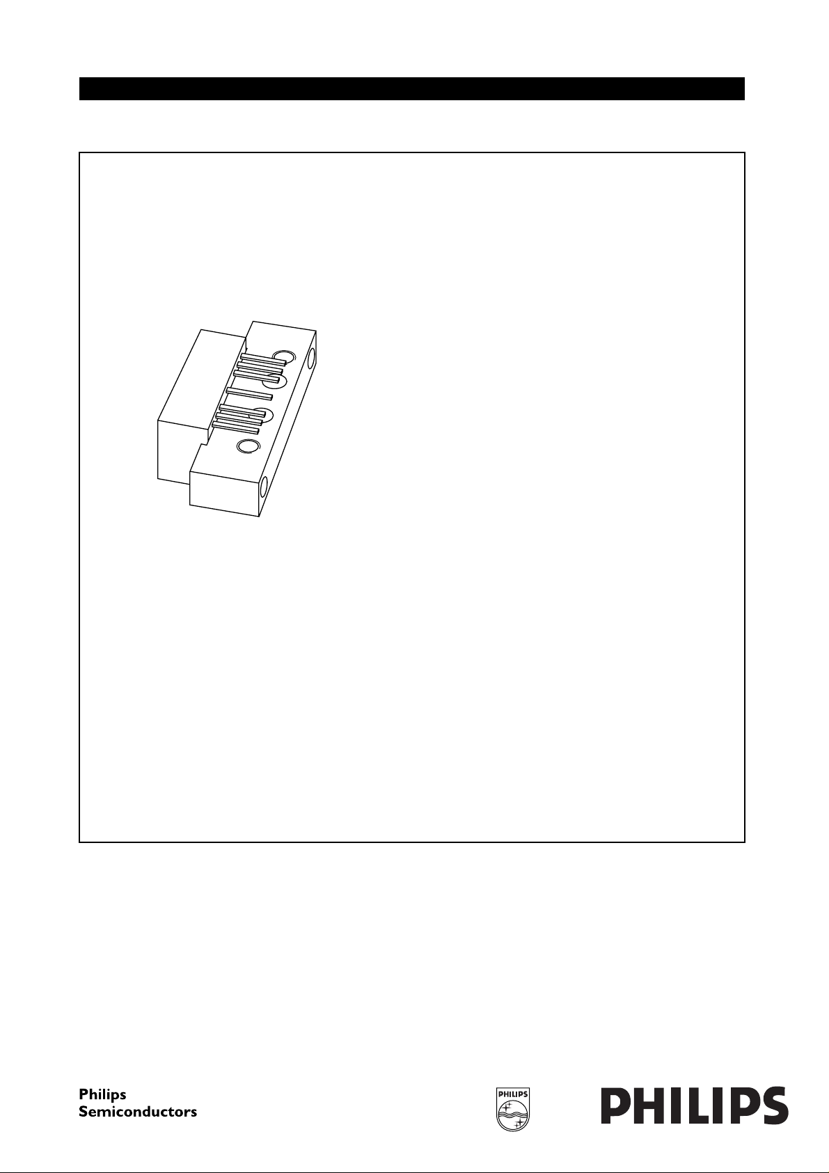
DISCRETE SEMICONDUCTORS
DATA SH EET
ook, halfpage
M3D252
CGY887
870 MHz, 21.5 dB gain
push-pull amplifier
Product specification
Supersedes data of 2002 June 07
2002 Jun 27
Page 2
Philips Semiconductors Product specification
870 MHz, 21.5 dB gain push-pull amplifier CGY887
FEATURES
• Superior linearity
• Extremely low noise
• Rugged construction
• Gold metallization ensures excellent reliability
• Excellent gain behaviour over temperature.
APPLICATIONS
• CATV systems operating in the 40 to 870 MHz
frequency range.
DESCRIPTION
Hybrid dynamic range amplifier module in a SOT115J
package operating with a voltage supply of 24 V (DC),
employing both GaAs and Si dies.
QUICK REFERENCE DATA
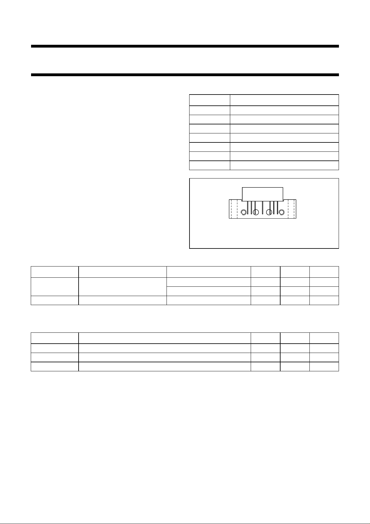
PINNING - SOT115J
PIN DESCRIPTION
1 input
2 common
3 common
5+V
B
7 common
8 common
9 output
handbook, halfpage
Side view
2
351
Fig.1 Simplified outline.
789
MSA319
SYMBOL PARAMETER CONDITIONS MIN. MAX. UNIT
G
p
power gain f = 50 MHz 21.2 21.8 dB
f = 870 MHz 22 23 dB
I
tot
total current consumption (DC) VB=24V − 240 mA
LIMITING VALUES
In accordance with the Absolute Maximum Rating System (IEC 60134).
SYMBOL PARAMETER MIN. MAX. UNIT
V
i
T
stg
T
mb
RF input voltage − 75 dBmV
storage temperature −40 +100 °C
operating mounting base temperature −20 +100 °C
2002 Jun 27 2
Page 3

Philips Semiconductors Product specification
870 MHz, 21.5 dB gain push-pull amplifier CGY887
CHARACTERISTICS
Bandwidth 40 to 870 MHz; VB= 24 V; Tmb=35°C; ZS=ZL=75Ω
SYMBOL PARAMETER CONDITIONS MIN. MAX. UNIT
G
p
SL slope straight line f = 45 to 870 MHz; note 1 0.6 1.4 dB
FL flatness straight line f = 45 to 100 MHz −±0.3 dB
s
11
s
22
s
21
CTB composite triple beat 79 chs flat; V
X
mod
CSO composite second order
d
2
V
o
power gain f = 45 MHz 21.2 21.8 dB
f = 870 MHz 22 23 dB
f = 100 to 800 MHz −±0.5 dB
f = 800 to 870 MHz −±0.3 dB
input return losses f = 45 to 80 MHz 20 − dB
f = 80 to 160 MHz 20 − dB
f = 160 to 320 MHz 20 − dB
f = 320 to 550 MHz 20 − dB
f = 550 to 650 MHz 19 − dB
f = 650 to 750 MHz 17 − dB
f = 750 to 870 MHz 17 − dB
output return losses f = 45 to 80 MHz 21 − dB
f = 80 to 160 MHz 19 − dB
f = 160 to 320 MHz 17 − dB
f = 320 to 550 MHz 16 − dB
f = 550 to 650 MHz 16 − dB
f = 650 to 750 MHz 16 − dB
f = 750 to 870 MHz 16 − dB
phase response f = 50 MHz −45 +45 deg
= 44 dBmV; fm= 547.25 MHz −−57 dB
o
112 chs flat; V
132 chs flat; V
= 44 dBmV; fm= 745.25 MHz −−55 dB
o
= 42 dBmV; fm= 859.25 MHz −−55 dB
o
cross modulation 79 chs flat; Vo= 44 dBmV; fm= 55.25 MHz −−53 dB
= 44 dBmV; fm= 55.25 MHz −−50 dB
o
= 42 dBmV; fm= 55.25 MHz −−52 dB
o
= 44 dBmV; fm= 548.5 MHz −−60 dB
o
112 chs flat; Vo= 44 dBmV; fm= 746.5 MHz −−55 dB
132 chs flat; Vo= 42 dBmV; fm= 860.5 MHz −−55 dB
132 chs flat; Vo= 42 dBmV; fm= 150 MHz −−65 dB
distortion
112 chs flat; V
132 chs flat; V
79 chs flat; V
CSO
sum
CSO
CSO
CSO
112 chs flat; Vo= 44 dBmV; fm= 150 MHz −−65 dB
dif
sum
dif
second order distortion note 2 −−58 dB
note 3 −−57 dB
note 4 −−57 dB
output voltage dim= −60 dB; note 5 64 − dBmV
d
= −60 dB; note 6 63 − dBmV
im
= −60 dB; note 7 62 − dBmV
d
im
2002 Jun 27 3
Page 4

Philips Semiconductors Product specification
870 MHz, 21.5 dB gain push-pull amplifier CGY887
SYMBOL PARAMETER CONDITIONS MIN. MAX. UNIT
NF noise figure f = 50 MHz − 5.5 dB
f = 100 MHz to f = 870 MHz − 5dB
I
tot
Notes
1. Slope straight line is defined as gain at 870 MHz against gain at 45 MHz.
2. fp= 55.25 MHz; Vp= 60 dBmV;
fq= 493.25 MHz; Vq= 60 dBmV;
measured at fp+fq= 548.5 MHz.
3. fp= 55.25 MHz; Vp= 60 dBmV;
fq= 691.25 MHz; Vq= 60 dBmV;
measured at fp+fq= 746.5 MHz.
4. fp= 55.25 MHz; Vp= 60 dBmV;
fq= 805.25 MHz; Vq= 60 dBmV;
measured at fp+fq= 860.5 MHz.
5. Measured according to DIN45004B:
fp= 540.25 MHz; Vp=Vo;
fq= 547.25 MHz; Vq=Vo−6 dB;
fr= 549.25 MHz; Vr=Vo−6 dB;
measured at fp+fq−fr= 538.25 MHz.
6. Measured according to DIN45004B:
fp= 740.25 MHz; Vp=Vo;
fq= 747.25 MHz; Vq=Vo−6 dB;
fr= 749.25 MHz; Vr=Vo−6 dB;
measured at fp+fq−fr= 738.25 MHz.
7. Measured according to DIN45004B:
fp= 851.25 MHz; Vp=Vo;
fq= 858.25 MHz; Vq=Vo−6 dB;
fr= 860.25 MHz; Vr=Vo−6 dB;
measured at fp+fq−fr= 849.25 MHz.
8. The module normally operates at VB= 24 V, but is able to withstand supply transients up to 30 V.
total current
consumption (DC)
note 8 − 240 mA
2002 Jun 27 4
Page 5
Philips Semiconductors Product specification
870 MHz, 21.5 dB gain push-pull amplifier CGY887
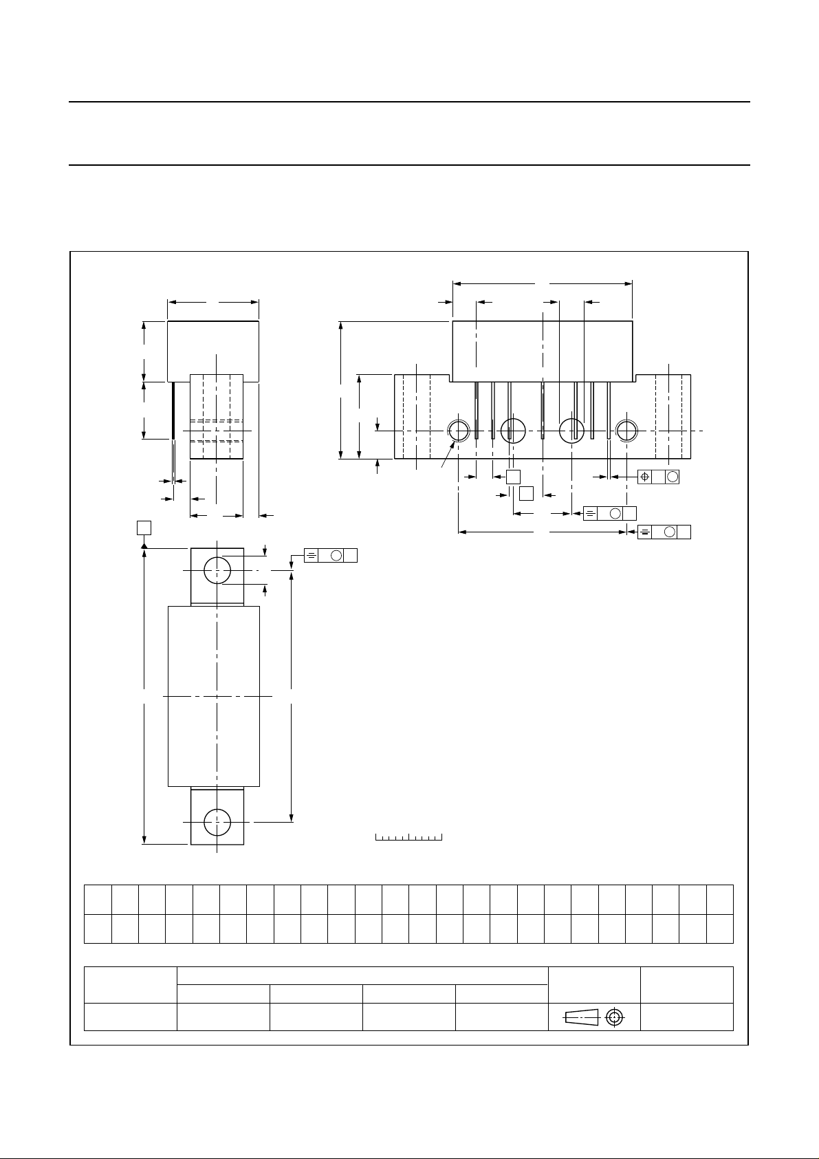
PACKAGE OUTLINE
Rectangular single-ended package; aluminium flange; 2 vertical mounting holes;
2 x 6-32 UNC and 2 extra horizontal mounting holes; 7 gold-plated in-line leads SOT115J
D
E
A
2
A
L
F
S
Z p
1
5
78923
c
d
U
Q
B
U
1
2
y M
p
q
B
0 5 10 mm
W
scale
e
e
1
b
q
2
q
1
y M
B
w
y M
M
B
DIMENSIONS (mm are the original dimensions)
A
UNIT
max.
max.
mm 20.8 9.1
OUTLINE
VERSION
SOT115J
A
2
c
bF
0.51
0.25 27.2 2.54 13.75 2.54 5.08 12.7 8.8
0.38
IEC JEDEC EIAJ
D
max.
d
max.
E
max.
ee
1
REFERENCES
L
min.
2002 Jun 27 5
Q
p
4.15
3.85
q
q1q
max.
2.4 38.1 25.4 10.2 4.2 44.75 8 0.25 0.1 3.8
2
U
1
S
max.
EUROPEAN
PROJECTION
W
U
2
6-32
UNC
yw
ISSUE DATE
99-02-06
Z
max.
Page 6

Philips Semiconductors Product specification
870 MHz, 21.5 dB gain push-pull amplifier CGY887
DATA SHEET STATUS
PRODUCT
DATA SHEET STATUS
Objective data Development This data sheet contains data from the objective specification for product
Preliminary data Qualification This data sheet contains data from the preliminary specification.
Product data Production This data sheet contains data from the product specification. Philips
(1)
STATUS
(2)
DEFINITIONS
development. Philips Semiconductors reserves the right to change the
specification in any manner without notice.
Supplementary data will be published at a later date. Philips
Semiconductors reserves the right to change the specification without
notice, in order to improve the design and supply the best possible
product.
Semiconductors reserves the right to make changes at any time in order
to improve the design, manufacturing and supply. Changes will be
communicated according to the Customer Product/Process Change
Notification (CPCN) procedure SNW-SQ-650A.
Notes
1. Please consult the most recently issued data sheet before initiating or completing a design.
2. The product status of the device(s) described in this data sheet may have changed since this data sheet was
published. The latest information is available on the Internet at URL http://www.semiconductors.philips.com.
DEFINITIONS
Short-form specification The data in a short-form
specification is extracted from a full data sheet with the
same type number and title. For detailed information see
the relevant data sheet or data handbook.
Limiting valuesdefinition Limiting values given are in
accordance with the Absolute Maximum Rating System
(IEC 60134). Stress above one or more of the limiting
values may cause permanent damage to the device.
These are stress ratings only and operation of the device
atthese or at anyotherconditions above those giveninthe
Characteristics sections of the specification is not implied.
Exposure to limiting values for extended periods may
affect device reliability.
Application information Applications that are
described herein for any of these products are for
illustrative purposes only. Philips Semiconductors make
norepresentationor warranty that such applications willbe
suitable for the specified use without further testing or
modification.
DISCLAIMERS
Life support applications These products are not
designed for use in life support appliances, devices, or
systems where malfunction of these products can
reasonably be expectedto result inpersonal injury. Philips
Semiconductorscustomersusingor selling these products
for use in such applications do so at their own risk and
agree to fully indemnify Philips Semiconductors for any
damages resulting from such application.
Right to make changes Philips Semiconductors
reserves the right to make changes, without notice, in the
products, including circuits, standard cells, and/or
software, described or contained herein in order to
improve design and/or performance. Philips
Semiconductors assumes no responsibility or liability for
theuseof any of theseproducts,conveysno licence or title
under any patent, copyright, or mask work right to these
products,and makes no representationsorwarranties that
these products are free from patent, copyright, or mask
work right infringement, unless otherwise specified.
CAUTION
This product is supplied in anti-static packing to prevent damage caused by electrostatic discharge during transport
and handling. For further information, refer to Philips specs.: SNW-EQ-608, SNW-FQ-302A, and SNW-FQ-302B.
2002 Jun 27 6
Page 7

Philips Semiconductors Product specification
870 MHz, 21.5 dB gain push-pull amplifier CGY887
NOTES
2002 Jun 27 7
Page 8

Philips Semiconductors – a w orldwide compan y
Contact information
For additional information please visit http://www.semiconductors.philips.com. Fax: +31 40 27 24825
For sales offices addresses send e-mail to: [email protected].
© Koninklijke Philips Electronics N.V. 2002
All rights are reserved. Reproduction in whole or in part is prohibited without the prior written consent of the copyright owner.
The information presented in this document does not form part of any quotation or contract, is believed to be accurate and reliable and may be changed
without notice. No liability will be accepted by the publisher for any consequence of its use. Publication thereof does not convey nor imply any license
under patent- or other industrial or intellectual property rights.
Printed in The Netherlands 613518/02/pp8 Date of release: 2002 Jun 27 Document order number: 9397 750 09935
SCA74
 Loading...