

Philips cgy2020g DATASHEETS
INTEGRATED CIRCUITS
DATA SH EET
CGY2020G
DCS 2 W power amplifier
Objective specification
File under Integrated Circuits, IC17
1996 Jul 17
Philips Semiconductors Objective specification
DCS 2 W power amplifier CGY2020G
FEATURES
• Power Amplifier (PA) overall efficiency 42%
• 33 dB gain
• 0 dBm input power
• Gain control range >50 dB
• Integrated power sensor driver
• Low output noise floor of PA <−121 dBm/Hz in DCS RX
band
• Wide operating temperature range −20 to +85 °C
• LQFP 48 pin package
• Compatible with power ramping controller PCA5075.
APPLICATIONS
• 1710 to 1785 MHz hand-held transceivers for DCS
applications
• 1800 MHz Time Division Multiple Access (TDMA)
systems.
QUICK REFERENCE DATA
SYMBOL PARAMETER
V
DD
I
DD
P
o(max)
T
amb
positive supply voltage − 4.5 − V
positive peak supply current − 1.1 − A
maximum output power − 33 − dBm
operating ambient temperature −20 − +85 °C
(1)
GENERAL DESCRIPTION
The CGY2020G is a DCS class 1 GaAs Monolithic
Microwave Integrated Circuit (MMIC) power amplifier
specifically designed to operate at 4.8 V battery supply.
The chip also includes a power sensor driver so that no
directional coupler is required in the power control loop.
The PA requires only a simple low-pass filter to comply
with the DCS transmit spurious specification. It can be
switched off and its power controlled by monitoring the
actual drain voltage applied to the amplifier stages.
MIN. TYP. MAX. UNIT
Note
1. For conditions, see Chapters “AC characteristics” and “DC characteristics”.
ORDERING INFORMATION
PACKAGE
TYPE NUMBER
NAME DESCRIPTION VERSION
CGY2020G LQFP48 plastic low profile quad flat package; 48 leads; body 7 x 7 x 1.4 mm SOT313-2
1996 Jul 17 2
Philips Semiconductors Objective specification
DCS 2 W power amplifier CGY2020G
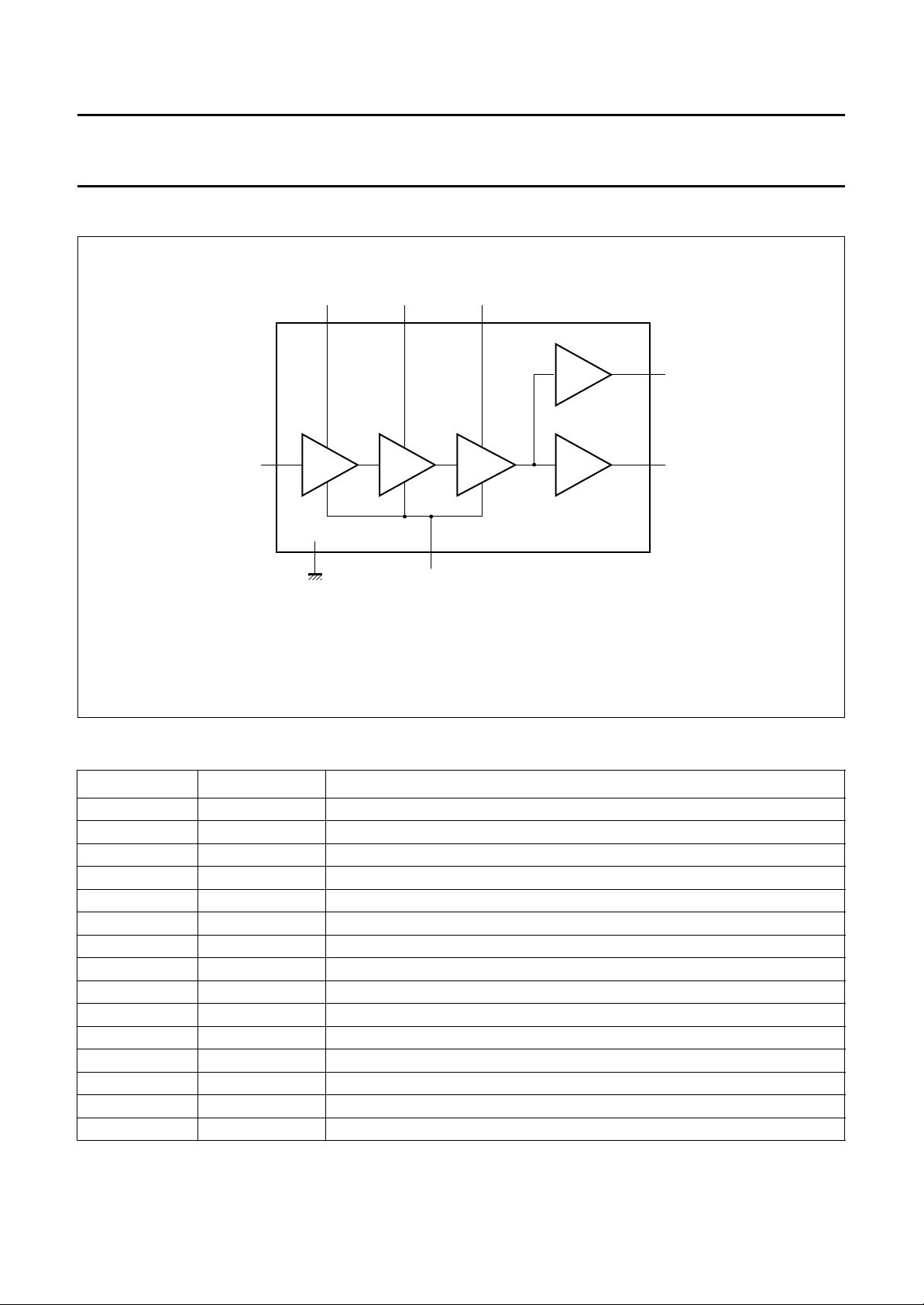
BLOCK DIAGRAM
handbook, full pagewidth
RFI
(1) Ground pins 1 to 7, 11 to 16, 18, 19, 21 to 26, 28 to 31, 33, 34, 36, 37 and 39 to 48.
V
DD1
38 27 20
35
(1)
GND
V
DD2
V
DD3
32
V
GG
Fig.1 Block diagram.
CGY2020G
SENSOR
DRIVER
8,9,10
MGG163
17
DETO/V
DD5
RFO/V
DD4
PINNING
SYMBOL PIN DESCRIPTION
GND 1 to 7 ground
RFO/V
DD4
8 to 10 PA output and fourth stage supply voltage
GND 11 to 16 ground
DETO/V
DD5
17 power sensor output and supply voltage
GND 18 and 19 ground
V
DD3
20 third stage supply voltage
GND 21 to 26 ground
V
DD2
27 second stage supply voltage
GND 28 to 31 ground
V
GG
32 negative gate supply voltage
GND 33 and 34 ground
RFI 35 PA input
GND 36 and 37 ground
V
DD1
38 first stage supply voltage
GND 39 to 48 ground
1996 Jul 17 3
Philips Semiconductors Objective specification
DCS 2 W power amplifier CGY2020G
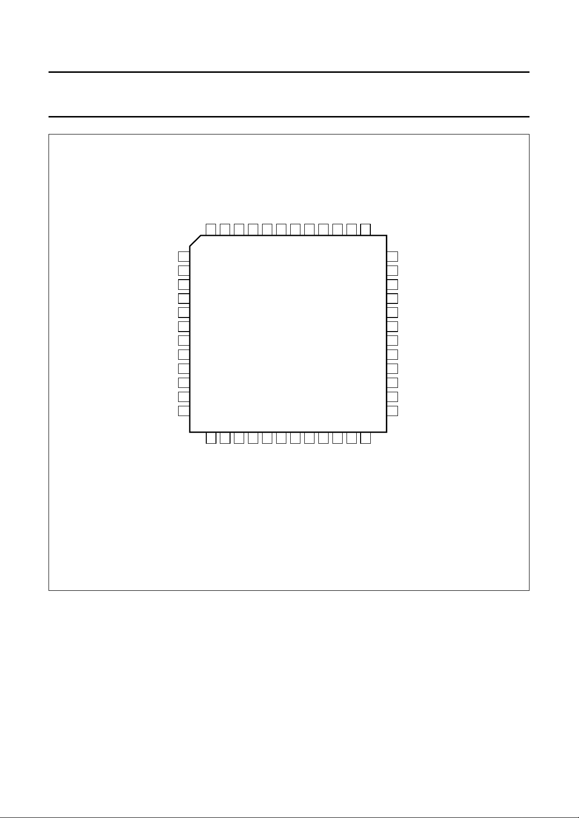
handbook, full pagewidth
RFO/V
RFO/V
RFO/V
GND
GND
GND
GND
GND
GND
GND
DD4
DD4
DD4
GND
GND
GND
GND
39
22
GND
DD1
V
38
23
GND
GND
24 37
GND
36
35
34
33
32
31
30
29
28
27
26
25
MGG162
GND
RFI
GND
GND
V
GG
GND
GND
GND
GND
V
DD2
GND
GND
GND
GND
47
14
GND
46
15
GND
GND
GND
45
44
CGY2020G
16
17
DD5
GND
DETO/V
GND
48
1
2
3
4
5
6
7
8
9
10
11
12
13
GND
GND
43
18
GND
GND
42
19
GND
GND
41
20
DD3
V
GND
40
21
Fig.2 Pin configuration.
1996 Jul 17 4
 Loading...