

Philips CGY2013G-C1 Datasheet

DATA SH EET
Preliminary specification
Supersedes data of 1996 Jul 12
File under Integrated Circuits, IC17
1998 Jan 23
INTEGRATED CIRCUITS
CGY2013G
GSM 4 W power amplifier

1998 Jan 23 2
Philips Semiconductors Preliminary specification
GSM 4 W power amplifier CGY2013G
FEATURES
• Power Amplifier (PA) overall efficiency 52%
• 35.5 dB gain
• 0 dBm input power
• Gain control range >55 dB
• Low output noise floor of PA < −130 dBm/Hz in GSM RX
band
• Wide operating temperature range −20 to +85 °C
• LQFP 48 pin package
• Compatible with power ramping controller PCF5077
• Compatible with GSM RF transceiver SA1620.
APPLICATIONS
• 880 to 915 MHz hand-held transceivers for E-GSM
applications
• 900 MHz Time Division Multiple Access (TDMA)
systems.
GENERAL DESCRIPTION
The CGY2013G is a GSM class 4 GaAs Monolithic
Microwave Integrated Circuit (MMIC) power amplifier
specifically designed to operate at 3.6 V battery supply.
The PA requires only a 30 dB harmonic low-pass filter to
comply with the GSM transmit spurious specification.
It can be switched off and its power controlled by
monitoring the actual drain voltage applied to the amplifier
stages.
QUICK REFERENCE DATA
Note
1. For conditions, see Chapters “AC characteristics” and “DC characteristics”.
ORDERING INFORMATION
SYMBOL PARAMETER
(1)
MIN. TYP. MAX. UNIT
V
DD
positive supply voltage − 3.6 − V
I
DD
positive peak supply current − 2.4 − A
P
o(max)
maximum output power − 35.5 − dBm
T
amb
operating ambient temperature −20 − +85
ο
C
TYPE
NUMBER
PACKAGE
NAME DESCRIPTION VERSION
CGY2013G LQFP48 plastic low profile quad flat package; 48 leads; body 7 × 7 × 1.4 mm SOT313-2
1998 Jan 23 3
Philips Semiconductors Preliminary specification
GSM 4 W power amplifier CGY2013G
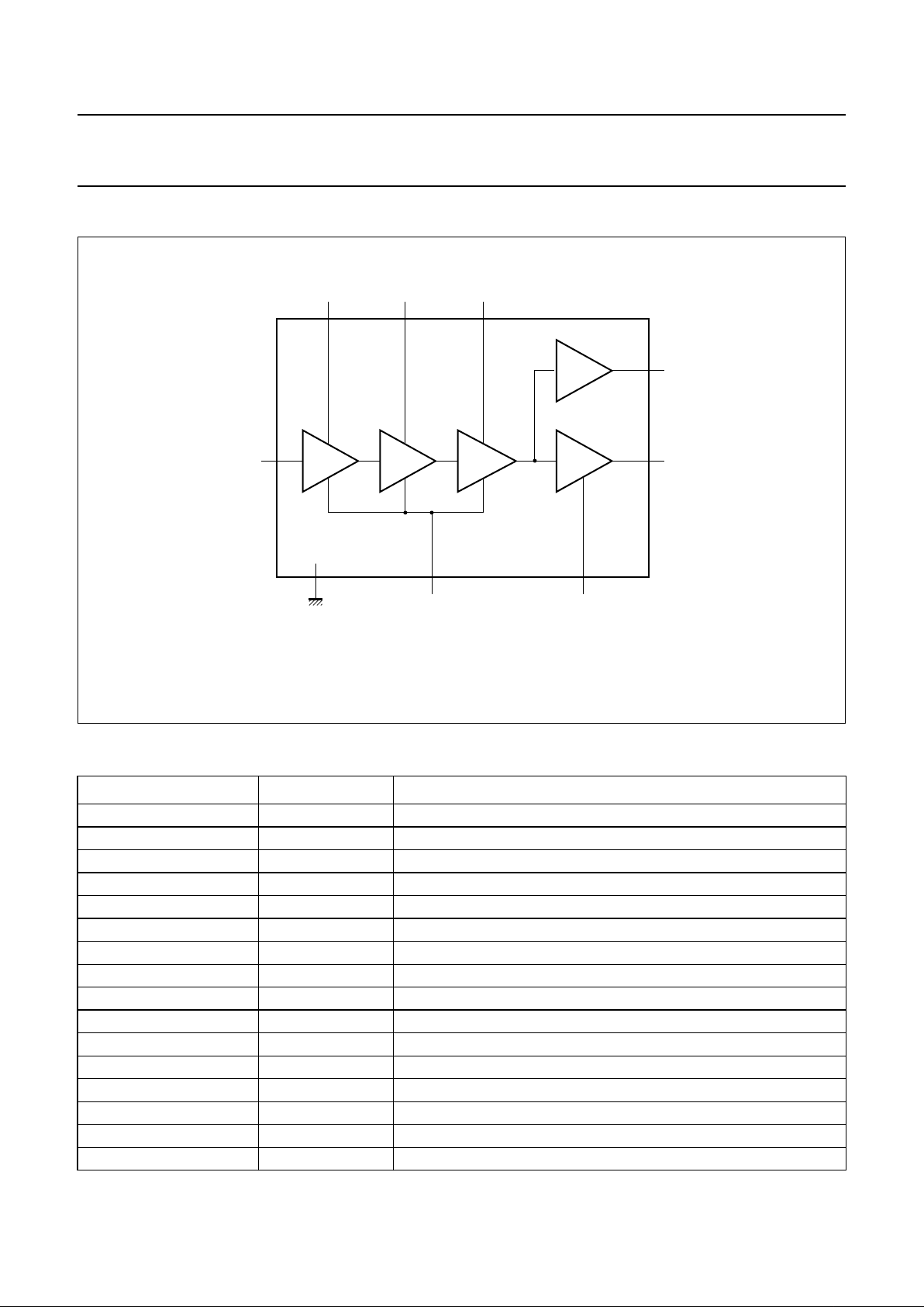
BLOCK DIAGRAM
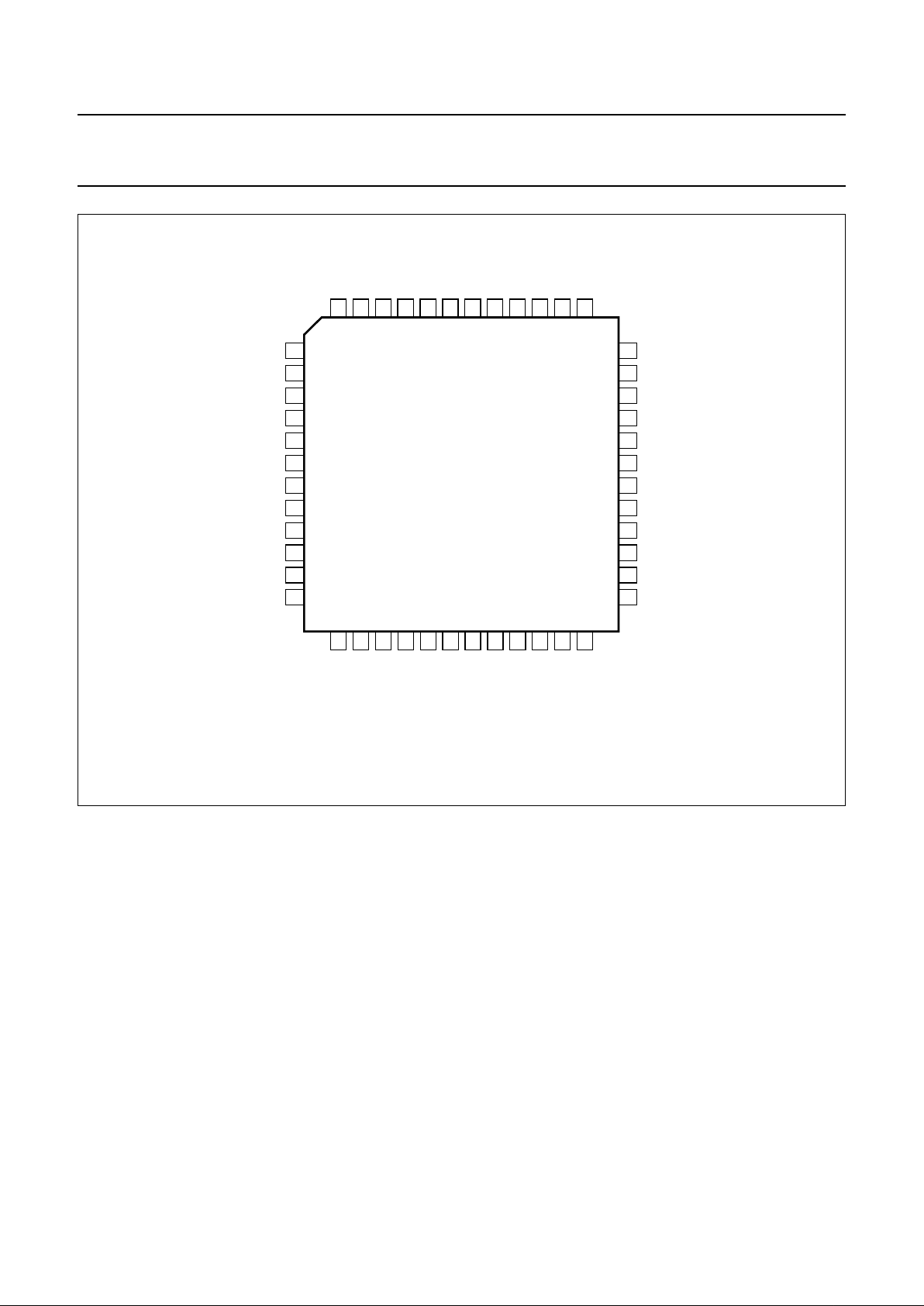
PINNING
SYMBOL PIN DESCRIPTION
GND 1 to 4 ground
RFO/V
DD4
5 to 8 power amplifier output and fourth stage supply voltage
GND 9 to 17 ground
DETO/V
DD5
18 power sensor output and supply voltage
V
GG2
19 fourth stage negative gate supply voltage
GND 20 to 26 ground
RFI 27 power amplifier input
GND 28 ground
V
DD1
29 first stage supply voltage
GND 30 ground
V
GG1
31 first three stages negative gate supply voltage
GND 32 ground
V
DD2
33 second stage supply voltage
GND 34 to 41 ground
V
DD3
42 third stage supply voltage
GND 43 to 48 ground
Fig.1 Block diagram.
(1) Ground pins 1 to 4, 9to 17, 20 to 26, 28, 30, 32, 34 to 41 and 43 to 48.
handbook, full pagewidth
CGY2013G
MGD627
(1)
31
19
18
5,6,7,8
29 33 42
27
GND
SENSOR
DRIVER
V
GG1
V
GG2
RFO/V
DD4
V
DD1
V
DD2
V
DD3
RFI
DETO/V
DD5
1998 Jan 23 4
Philips Semiconductors Preliminary specification
GSM 4 W power amplifier CGY2013G
Fig.2 Pin configuration.
handbook, full pagewidth
1
2
3
4
5
6
7
8
9
10
11
36
35
34
33
32
31
30
29
28
27
26
13
14
15
16
17
18
19
20
21
22
23
48
47
46
45
44
43
42
41
40
39
38
12
24 37
25
CGY2013G
MGD628
GND
GND
GND
V
DD2
V
GG1
GND
V
DD1
GND
RFI
GND
GND
GND
GND
GND
GND
RFO/V
DD4
RFO/V
DD4
RFO/V
DD4
GND
GND
GND
GND
GND
GND
GND
GND
GND
GND
V
DD3
GND
GND
GND
GND
GND
GND
RFO/V
DD4
GND
GND
GND
GND
DETO/V
DD5
V
GG2
GND
GND
GND
GND
GND
GND
FUNCTIONAL DESCRIPTION
Operating conditions
The CGY2013G is designed to meet the European
Telecommunications Standards Institute (ETSI) GSM
documents, the
“ETS 300 577 specification”
, which are
defined as follows:
• ton= 542.8 µs
• T = 4.3 ms
• Duty cycle = 1/8.
The device is specifically designed for pulse operation
allowing the use of a LQFP48 plastic package.
Power amplifier
The power amplifier consists of four cascaded gain stages
with an open-drain configuration. Each drain has to be
loaded externally by an adequate reactive circuit which
also has to be a DC path to the supply.
The amplifier bias is set using a negative voltage applied
at pins V
GG1
and V
GG2
. This negative voltage must be
present before the supply voltage is applied to the drains
to avoid current overstress for the amplifier.
 Loading...