

Page 1

Car entertainment system
CEM2000/00/55/51
CEM2000X/78
CONTENTS
Technical specification ..................................................................1-2
Service measurement setup..........................................................1-3
Service aids .................................................................................1-4
Instructions on CD playability ...............................................2-1.. 2-2
Block diagram ................................................................................3-1
Wiring diagram ..............................................................................4-1
Main board
Circuit diagram ..................................................................5-1..5-5
Layout diagram..................................................................5-6..5-7
Panel board
Circuit diagram .........................................................................6-1
Layout diagram..................................................................6-2..6-3
Servo board
Circuit diagram..........................................................................7-1
Layout diagram ..................................................................7-2..7-3
Exploded view diagram .................................................................8-1
Revision list ...................................................................................9-1
©
Copyright 2010 Philips Consumer Electronics B.V. Eindhoven, The Netherlands
All rights reserved. No part of this publication may be reproduced, stored in a retrieval
system or transmitted, in any form or by any means, electronic, mechanical, photocopying,
or otherwise without the prior permission of Philips.
Published by LX 1046 Service Audio Subject to modification
Version 1.1
3141 785 35131
Page 2
TECHNICAL SPECIFICATION
1 - 2
General inforamtion
Power supply 12 V DC (11 V - 16
V), negative ground
Fuse 15 A
Suitable speaker
4 - 8
impedance
Maximum power
45 W x 4 channels
output
Continuous power
output
Pre-Amp output
22 W x 4 RMS (4
10% T.H.D.)
2.0 V
voltage
Aux-in level
500 mV
Dimensions
(W x H x D) 188 x 58 x 201 mm
Weight 1.47 kg
VERSION VARIATION
Type /Versions:
Board in used:
SERVO BOARD
MAIN BOARD
Service policy
/00 /00
Europe
C
C
APAC
C/M
C/M
Radio
Frequency range
- FM
Frequency range
- AM(MW)
Usable sensitivity
- FM
Usable sensitivity
- AM(MW) (S/N
= 20 dB)
CEM2000
/55
C/M
C/M
87.5 - 108.0 MHz (100kHz
per step in auto search and
50kHz per step in manual
search)
522 - 1620 KHz (9 kHz)
530 - 1710 kHz (10 kHz)
8 µV
30 µV
15/16/85/
C
C
Type /Versions:
Features
RDS
VOLTAGE SELECTOR
ECO STANDBY - DARK
* TIPS : C -- Component Lever Repair.
M -- Module Lever Repair
-- Used
Feature diffrence
/05 /12
CEM2000
/55
15/16/85/
Page 3
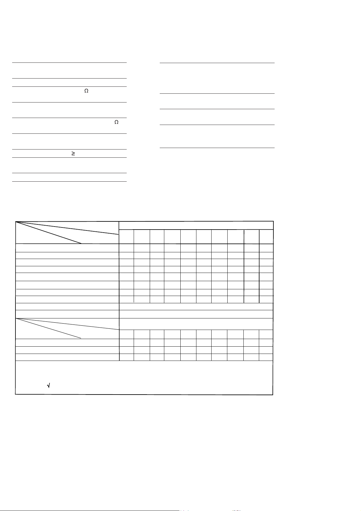
e
MEASUREMENT SETUP
Tuner FM
1-3
Bandpass
LF Voltmeter
e.g. PM2534
RF Generator
e.g. PM5326
DUT
250Hz-15kHz
e.g. 7122 707 48001
Ri=50:
S/N and distortion meter
e.g. Sound Technology ST1700B
Use a bandpass filter to eliminate hum (50Hz, 100Hz) and disturbance from the pilottone (19kHz, 38kHz).
Tuner AM (MW,LW)
RF Generator
e.g. PM5326
Ri=50:
DUT
Frame aerial
e.g. 7122 707 89001
Bandpass
250Hz-15kHz
e.g. 7122 707 48001
LF Voltmeter
e.g. PM2534
S/N and distortion meter
e.g. Sound Technology ST1700B
To avoid atmospheric interference all AM-measurements have to be carried out in a Faraday´s cage.
Use a bandpass filter (or at least a high pass filter with 250Hz) to eliminate hum (50Hz, 100Hz).
CD
Use Audio Signal Disc
(replaces test disc 3)
DUT
L
R
SBC429 4822 397 30184
S/N and distortion meter
e.g. Sound Technology ST1700B
LEVEL METER
e.g. Sennheiser UPM550
-
Recorder
Use Universal Test Cassette CrO2 SBC419 4822 397 30069
or Universal Test Cassette
LF Generator
e.g. PM5110
Fe SBC420 4822 397 30071
DUT
L
R
S/N and distortion met
e.g. Sound Technology ST170
LEVEL METER
e.g. Sennheiser UPM550
with FF-filter
Page 4
SERVICE AIDS
1-4
GB
All ICs and many other semi-conductors are
susceptible to electrostatic discharges (ESD).
Careless handling during repair can reduce life
drastically.
When repairing, make sure that you are
connected with the same potential as the mass
of the set via a wrist wrap with resistance.
Keep components and tools also at this
potential.
WARNING
GB
Safety regulations require that the set be restored to its original
condition and that parts which are identical with those specified,
be used
Safety components are marked by the symbol
!
.
ESD
CLASS 1
LASER PRODUCT
Lead free
Page 5
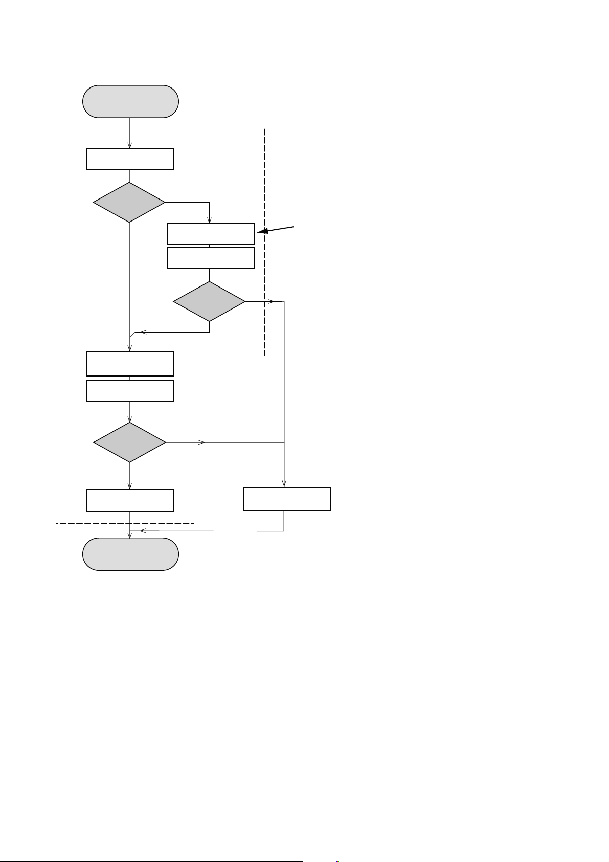
INSTRUCTIONS ON CD PLAYABILITY
Customer complaint
"CD related problem"
Set remains closed!
check playability
1
2 - 1
playability
ok ?
Y
Play a CD
for at least 10 minutes
check playability
playability
ok ?
Y
N
"fast" lens cleaning
check playability
playability
ok ?
N
3
N
Y
For flap loaders (= access to CD drive possible)
cleaning method
4 is recommended
add Info for customer
"SET OK"
2
return set
1 - 4 For description - see following pages
Exchange CDM
Page 6
INSTRUCTIONS ON CD PLAYABILITY
2 - 2
1
PLAYABILITY CHECK
For sets which are compatible with CD-RW discs
use CD-RW Printed Audio Disc ....................7104 099 96611
TR 3 (Fingerprint)
TR 8 (600µ Black dot) maximum at 01:00
• playback of these two tracks without audible disturbance
playing time for: Fingerprint
Black dot from 00:50 to 01:10
• jump forward/backward (search) within a reasonable time
For all other sets
use CD-DA SBC 444A..................................4822 397 30245
TR 14 (600µ Black dot) maximum at 01:15
TR 19 (Fingerprint)
TR 10 (1000µ wedge)
• playback of all these tracks without audible disturbance
playing time for: 1000µ wedge 10seconds
Fingerprint 10seconds
Black dot from 01:05 to 01:25
• jump forward/backward (search) within a reasonable time
10seconds
4
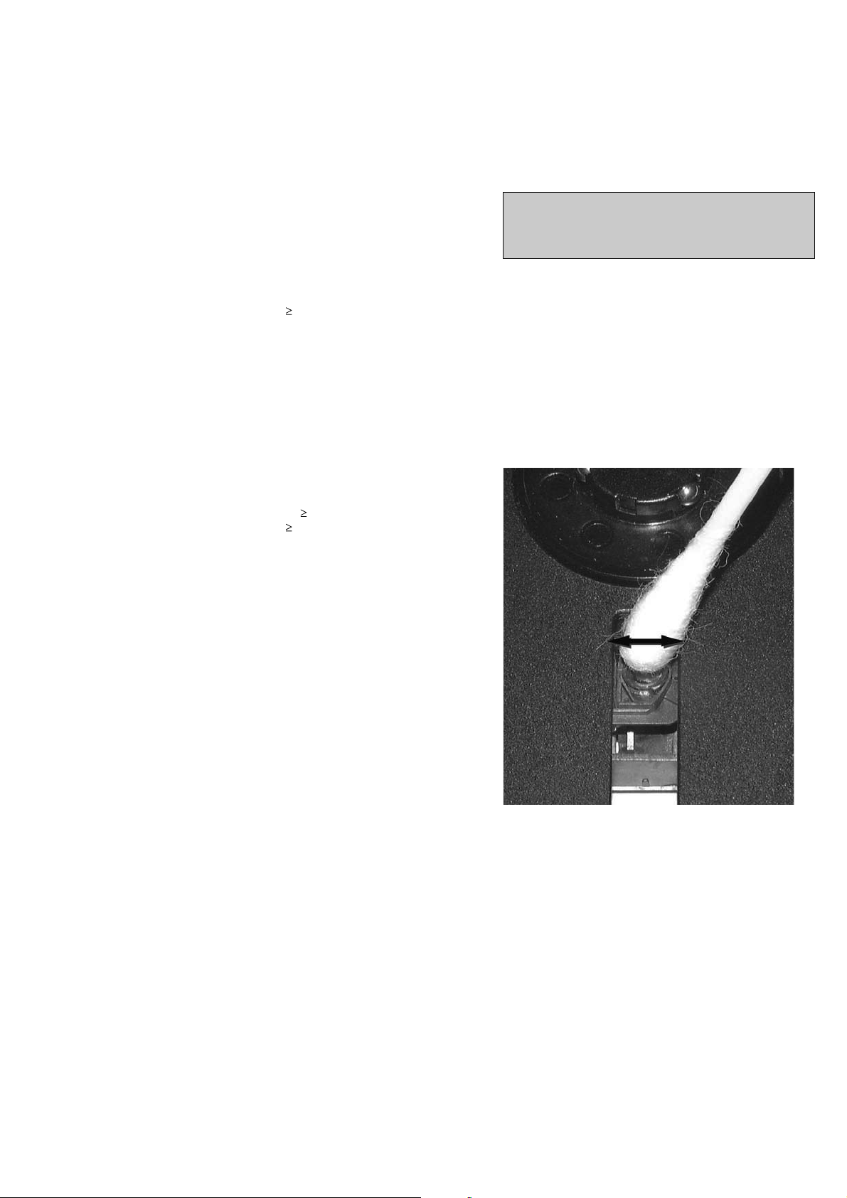
LIQUID LENS CLEANING
Before touching the lens it is advised to clean the
surface of the lens by blowing clean air over it.
This to avoid that little particles make scratches on
the lens.
Because the material of the lens is synthetic and coated
with a special anti-reflectivity layer, cleaning must be done
with a non-aggressive cleaning fluid. It is advised to use
“Cleaning Solvent
The actuator is a very precise mechanical component and
may not be damaged in order to guarantee its full function.
Clean the lens gently (don’t press too hard) with a soft and
clean cotton bud moistened with the special lens cleaner.
The direction of cleaning must be in the way as indicated in
the picture below.
2
CUSTOMER INFORMATION
It is proposed to add an addendum sheet to the set which
informs the customer that the set has been checked
carefully - but no fault was found.
The problem was obviously caused by a scratched, dirty or
copy-protected CD. In case problems remain, the customer
is requested to contact the workshop directly.
The lens cleaning (method 3) should be mentioned in the
addendum sheet.
The final wording in national language as well as the printing
is under responsibility of the Regional Service Organizations.
Page 7
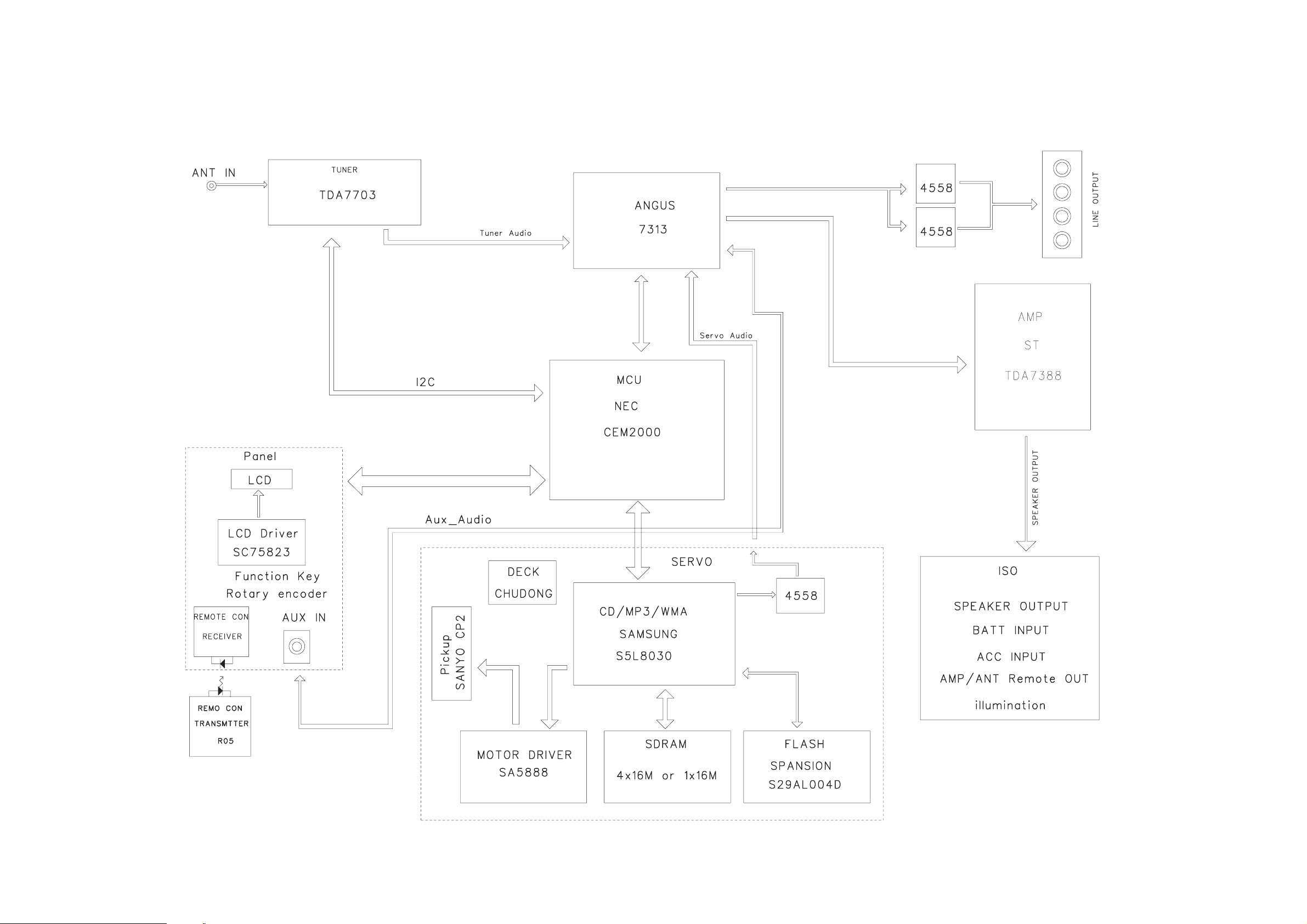
SET BLOCK DIAGRAM
3 - 1
3 - 1
Page 8
S5L8030
8M FLASH
1117-ADJ
4x16M SDRAM
SA5888 MOTOR DRIVOE
4558
1117-3.3V
AMP TDA7388
LINE OUT
ANT
ISO
RADIO TDA7703
4558
VOL IC 7313
7809
20Pin FFC
MCU
22Pin Connector
TO PANEL
Wiring diagram
SERVO Board
Main Board
20Pin FFC
+5V IC
Reset sw
Page 9
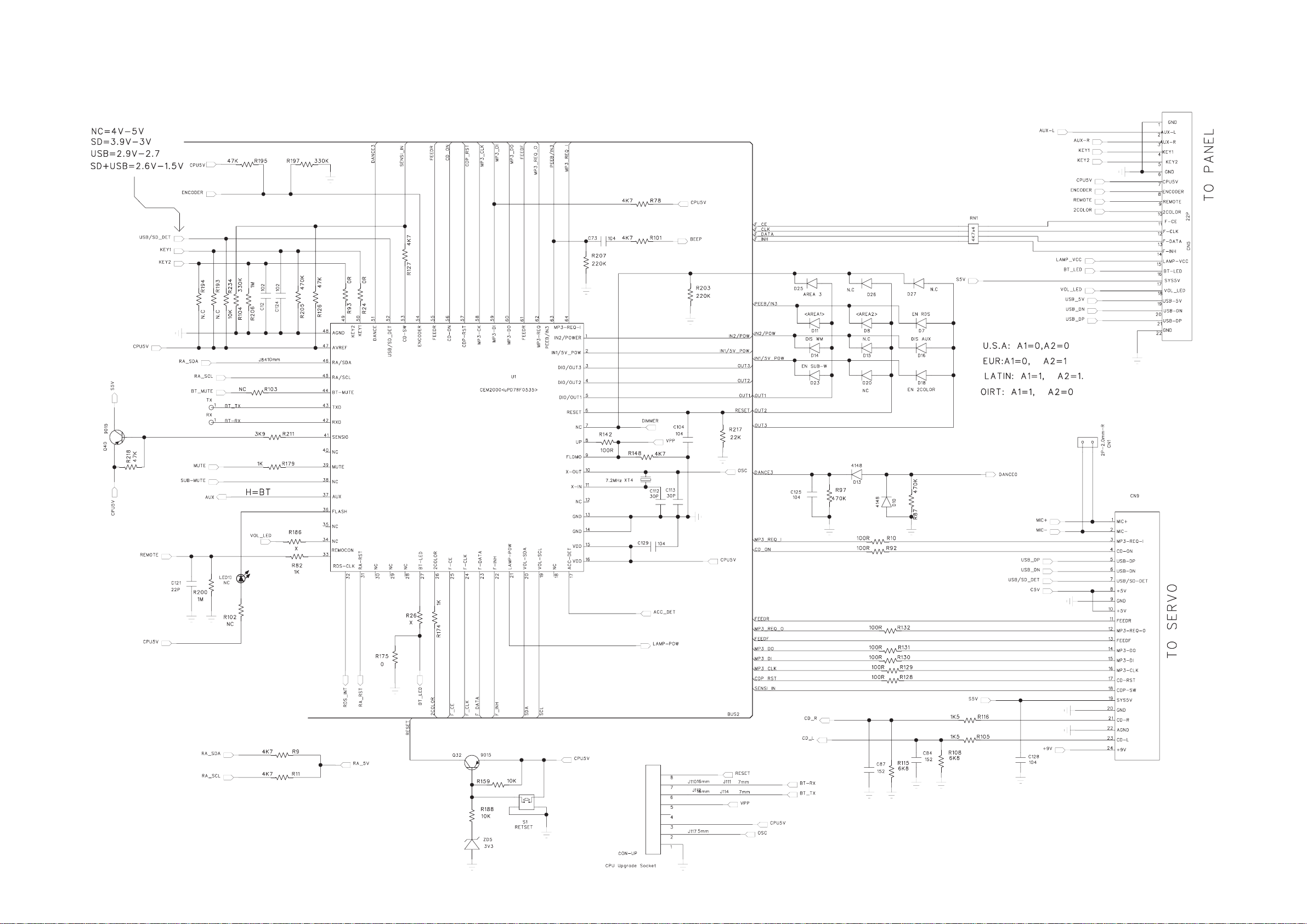
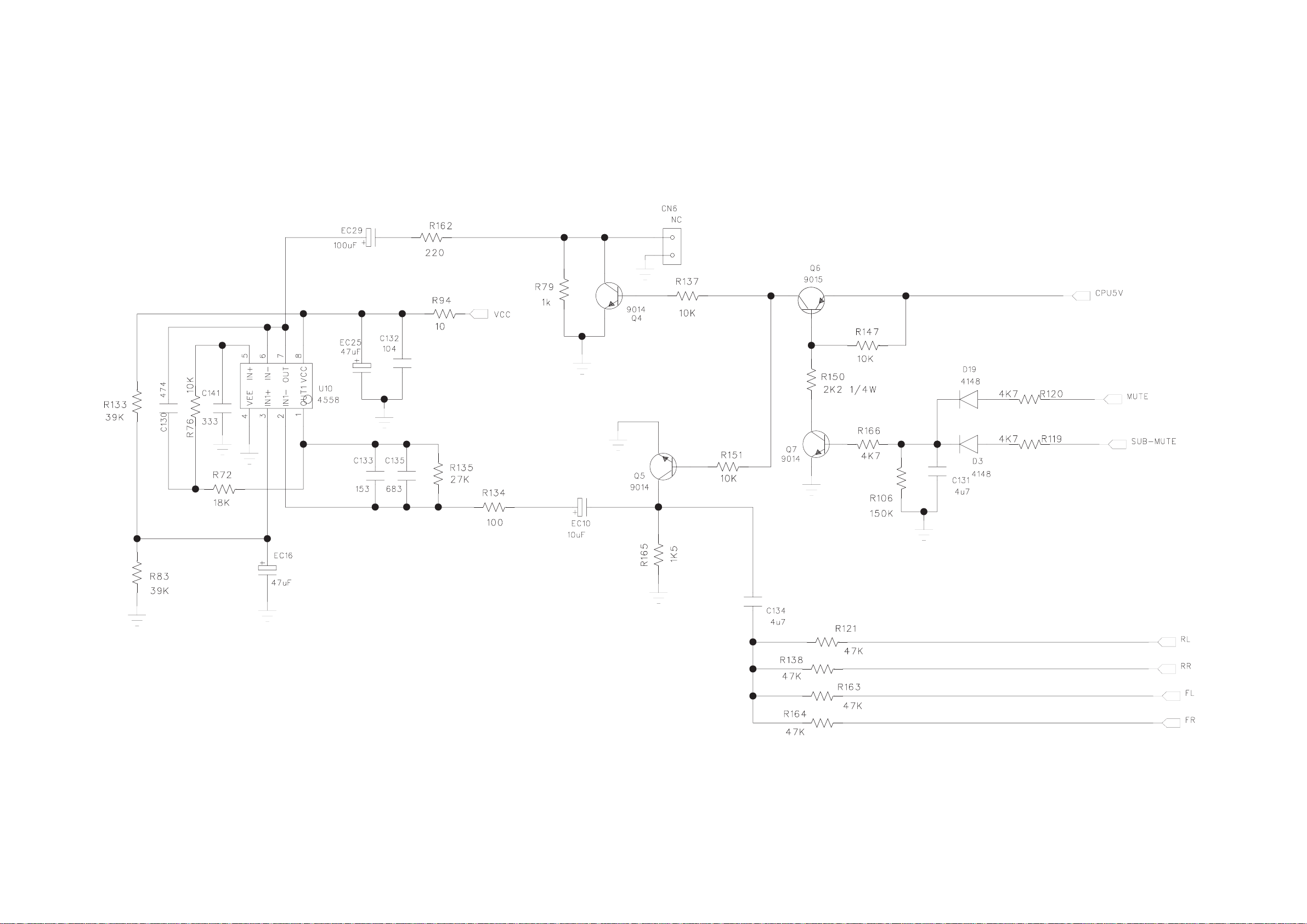
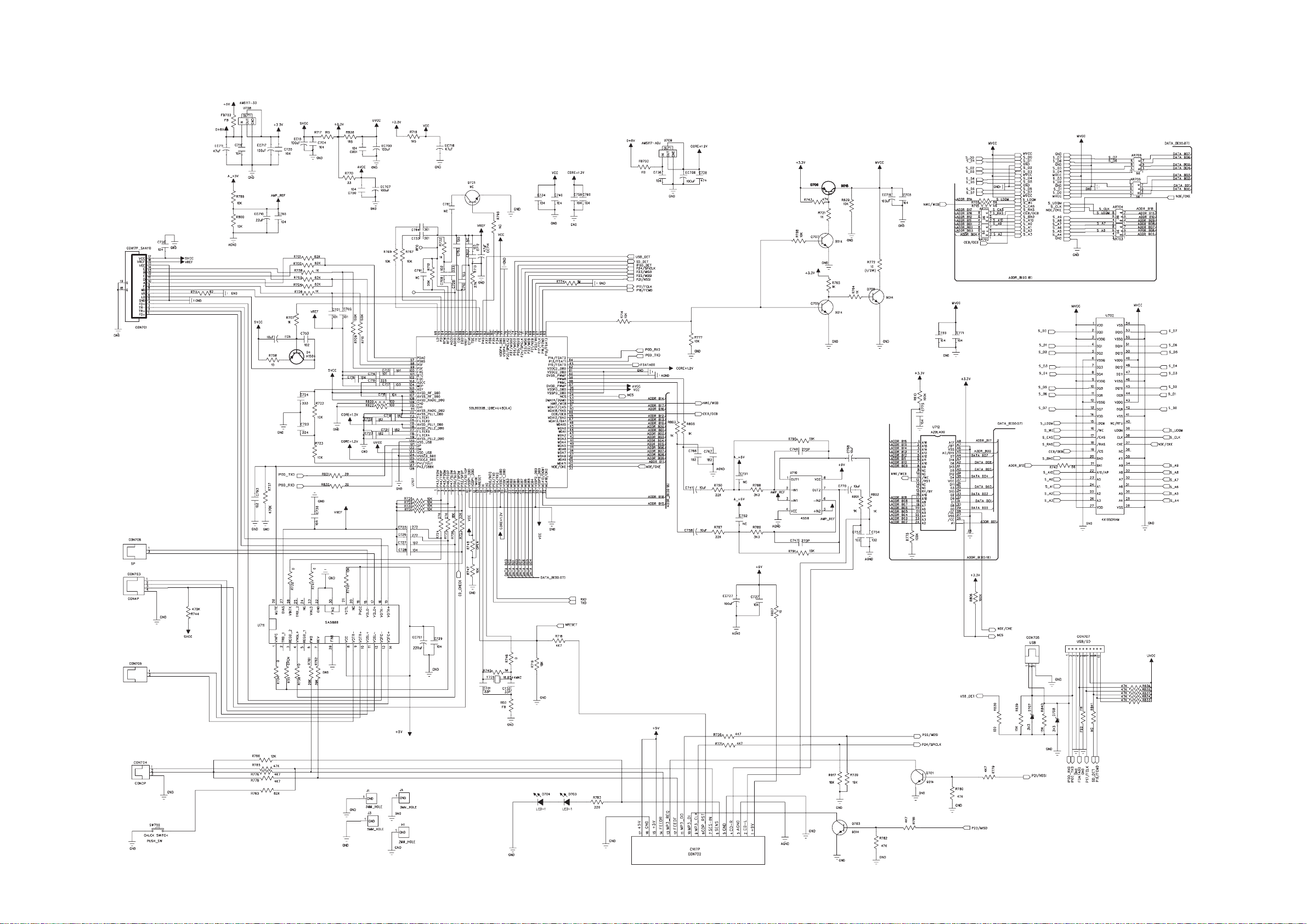
CIRCUIT DIAGRAM - MAIN BOARD
MCU PART
5 - 15 - 1
Page 10
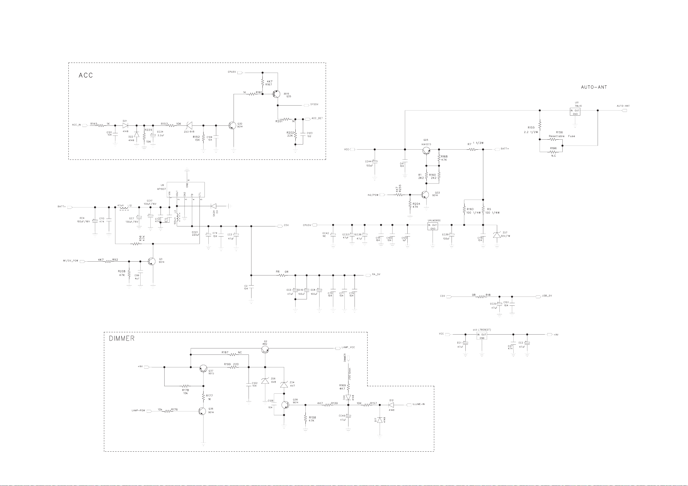
CIRCUIT DIAGRAM - MAIN BOARD
Power PART
5 - 2
5 - 2
Page 11
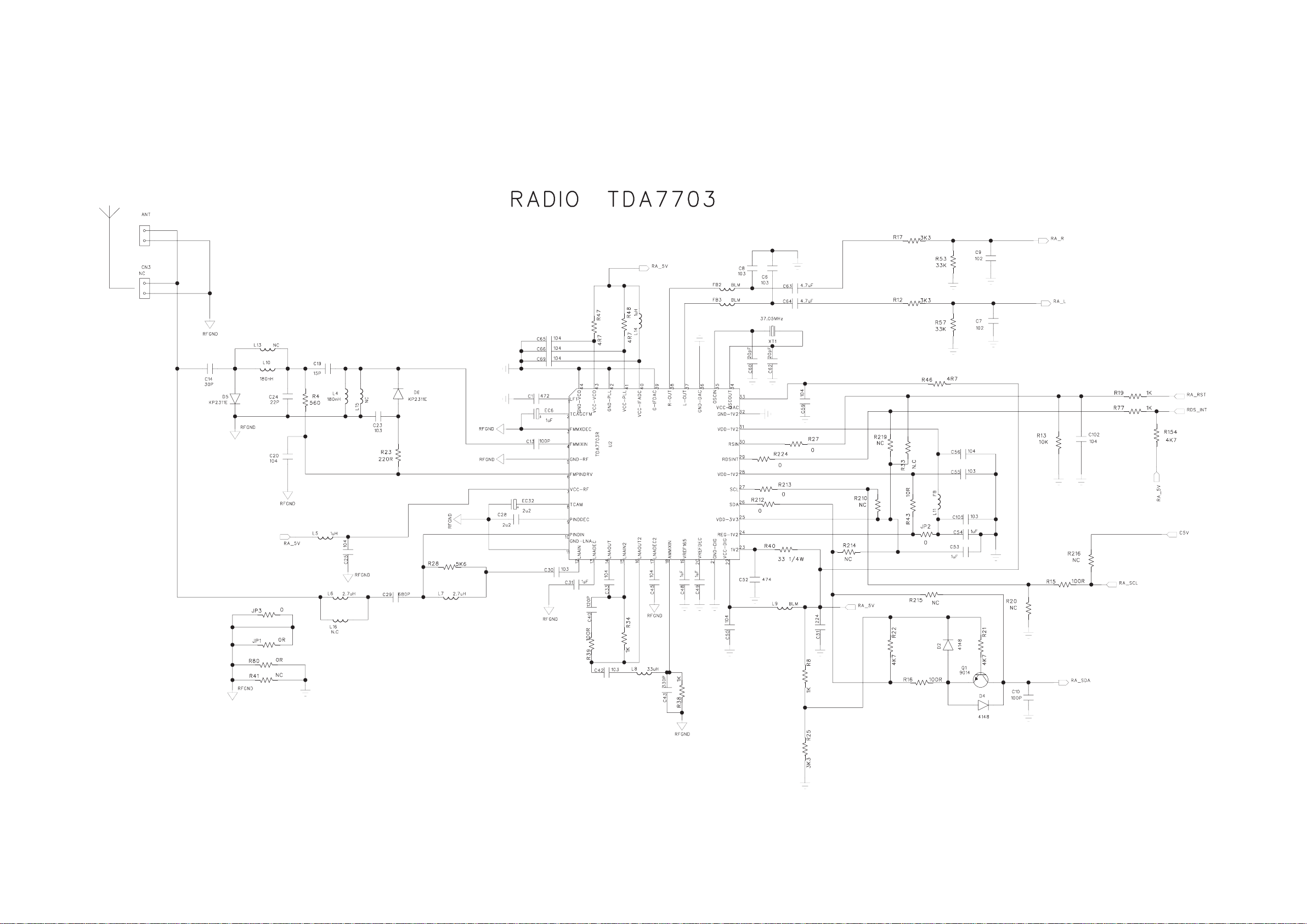
CIRCUIT DIAGRAM - MAIN BOARD
Radio PART
5 - 3
5 - 3
Page 12
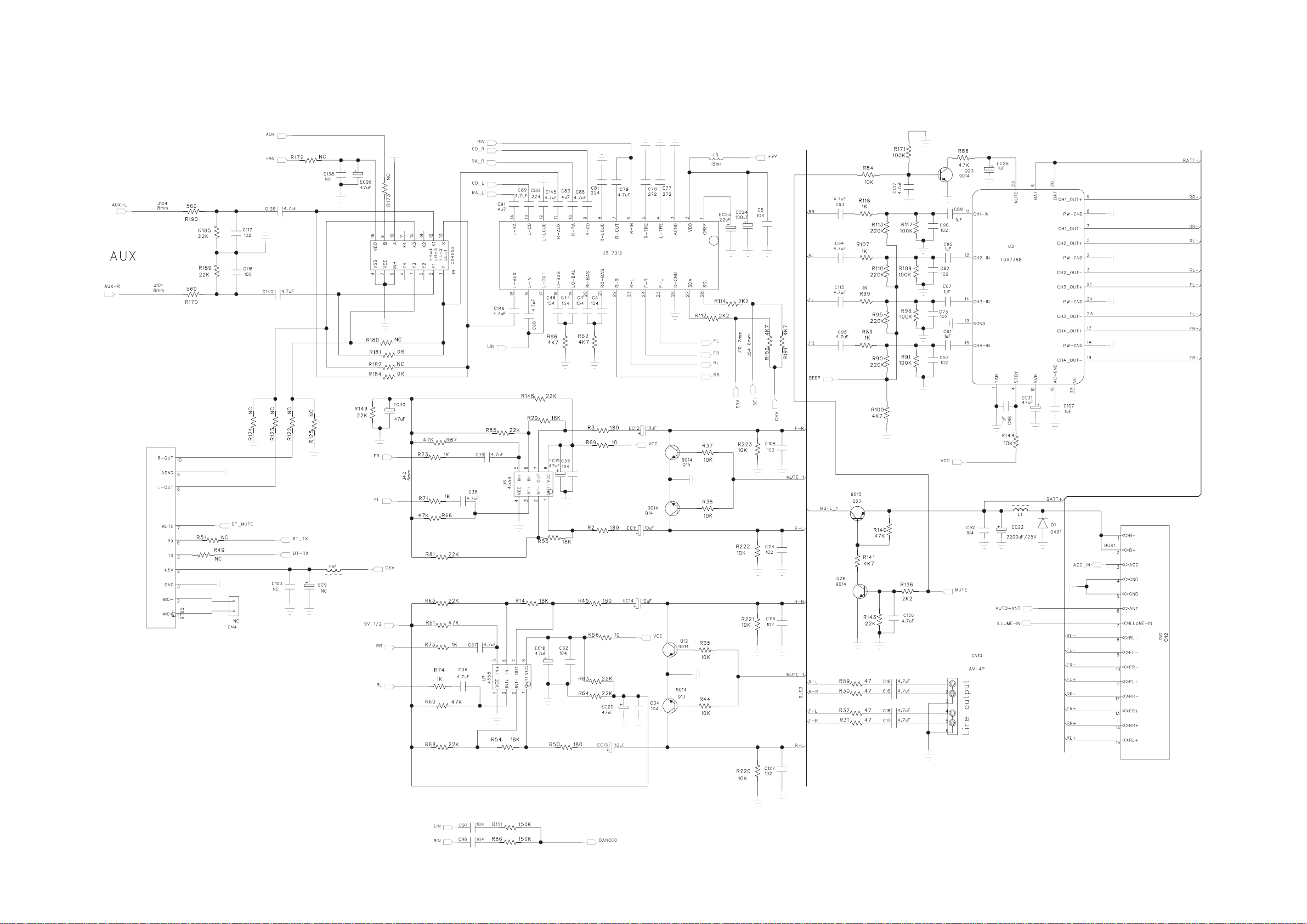
CIRCUIT DIAGRAM - MAIN BOARD
Audio PART 1
5 - 4 5 - 4
Page 13
CIRCUIT DIAGRAM - MAIN BOARD
Audio PART 2
5 - 5 5 - 5
Page 14
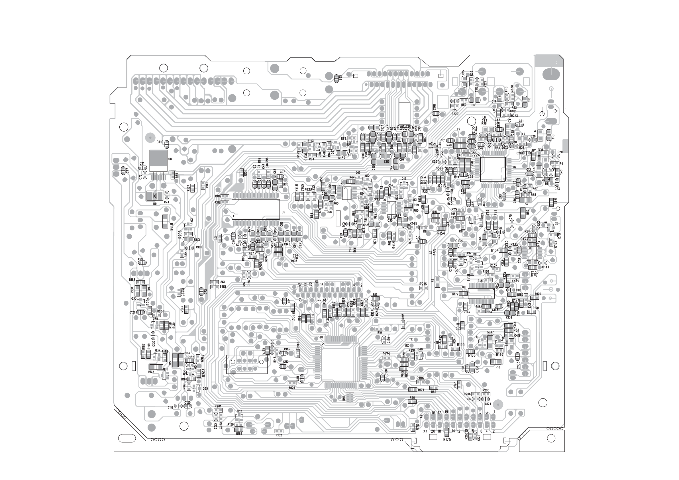
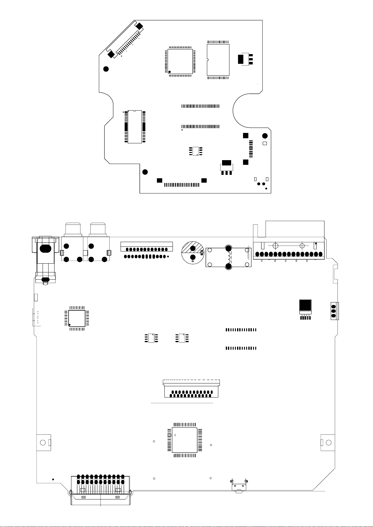
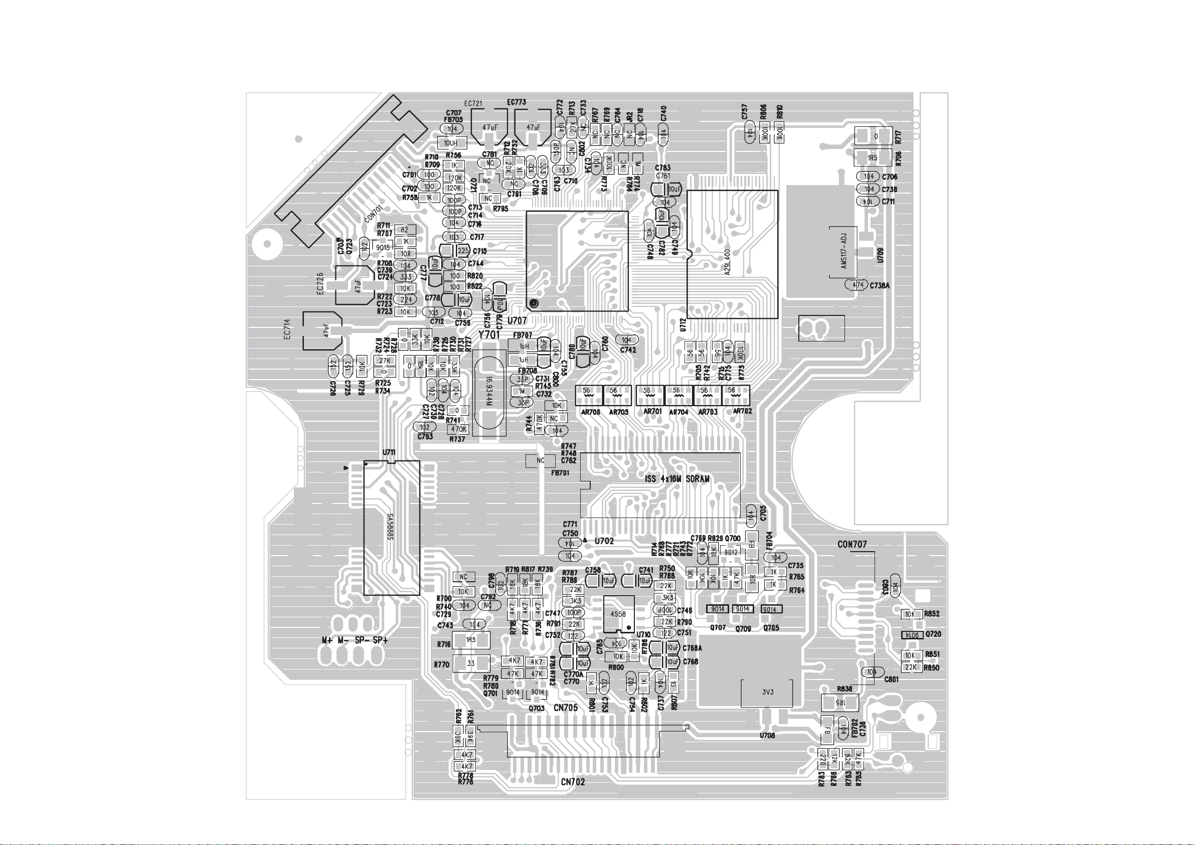
LAYOUT DIAGARM - MAIN BOARD
TOP SIDE VIEW
5 - 6
5 - 6
Page 15
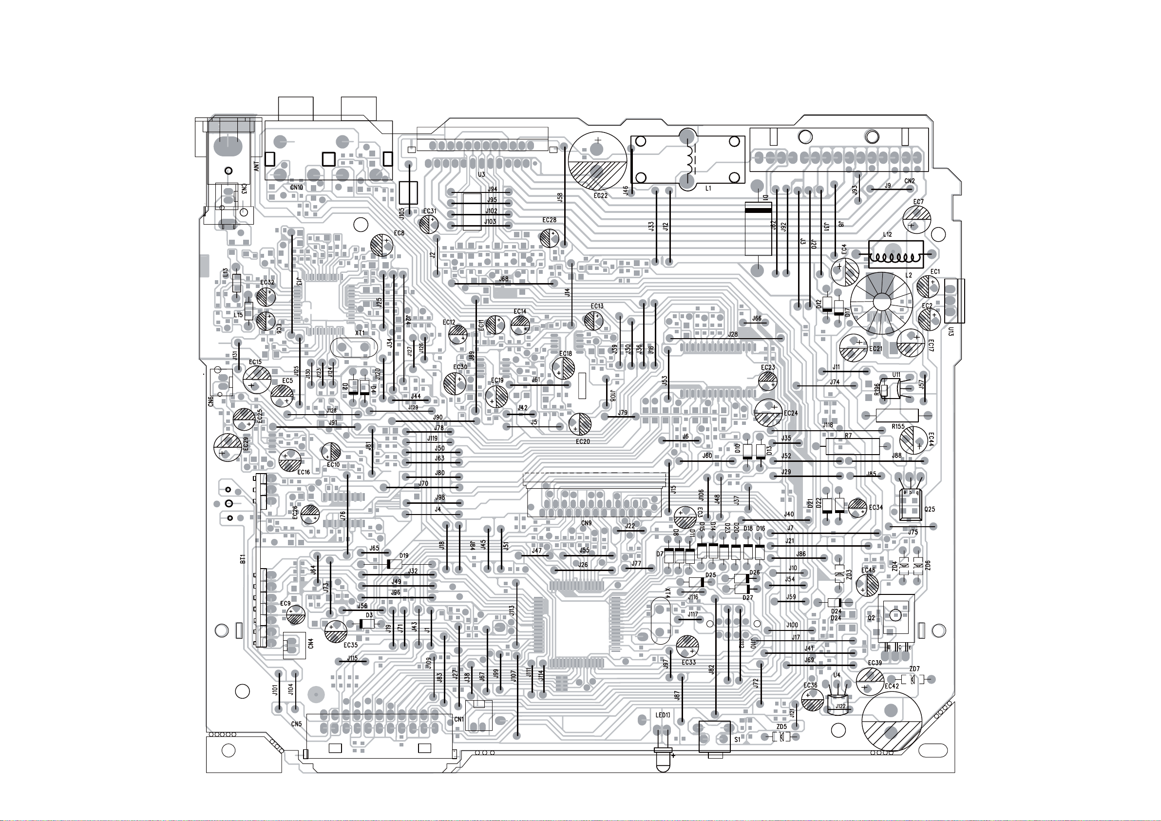
LAYOUT DIAGARM - MAIN BOARD
BOTTOM SIDE VIEW
5 - 7
5 - 7
Page 16
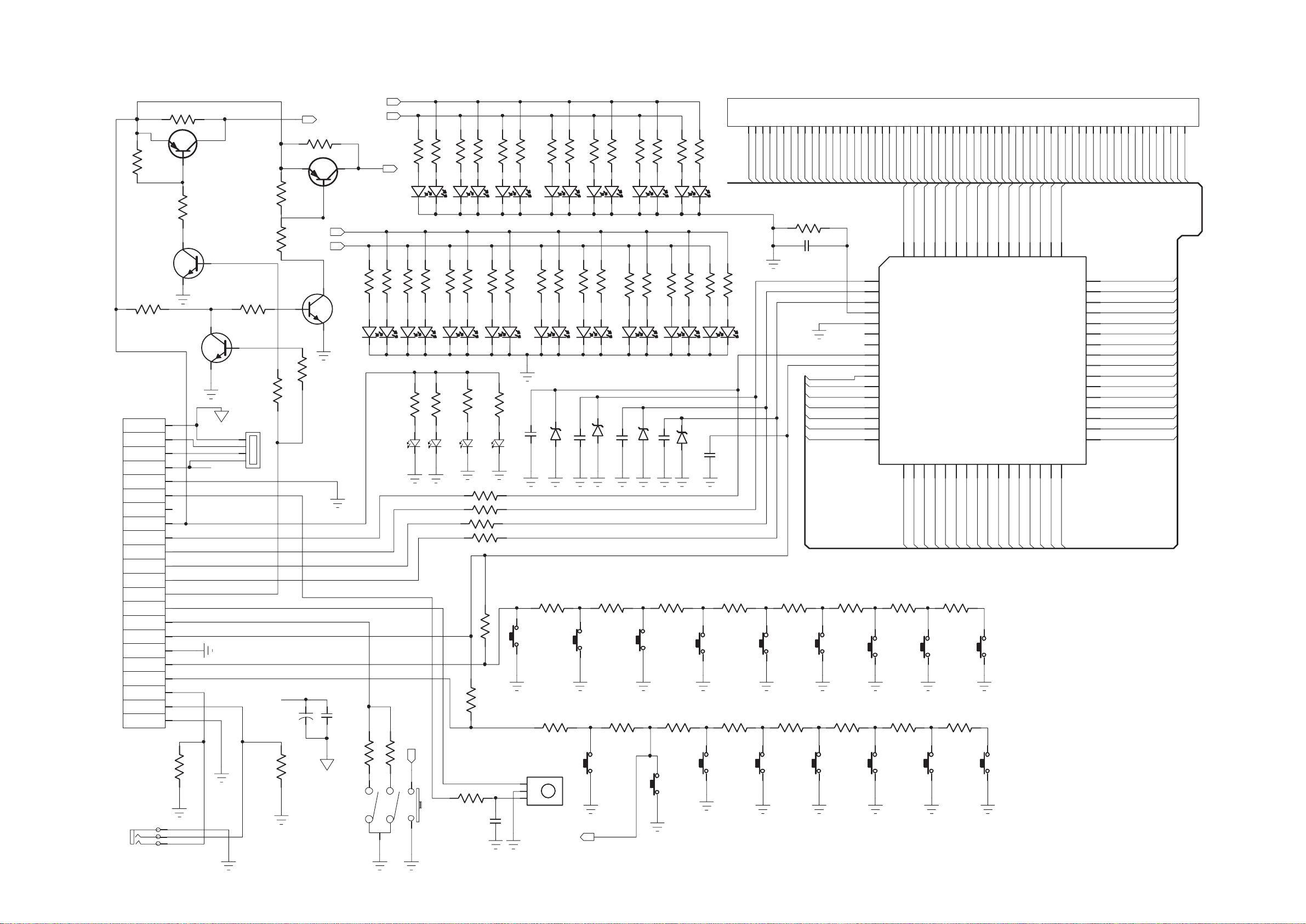
CIRCUIT DIAGARM - PANEL BOARD
6 - 1 6 - 1
R935
CON1
AUX IN
NC
USB_UP
USB_DN
USB_5V
GND
SYS_5V
BT_LED
LAMP_VCC
2COLOR
REMOTE
ENCODER
24PIN-CON
KEY 2
AUX_R
AUX_L
GND
AUX1
NC
R936
GND
INH
DATA
CLK
CE
+5V
GND
KEY 1
Q904
ZR902
22P
R939
NC
1
2
3
R963
RED+8V
NC
RED+8V
Q901
NC
NC
R938
NC
R937
RED+8V
BLUE+8V
R965
NC
NC
Q905
NC
NC
R966
R934
USB-GND
22
21
20
19
USB+5V
1
2
USB
3
USBIN
4
18
17
16
15
14
BLUE+8V
270
NC
390
390
NC
270
NC
R9640R
270
NC
270
NC
390
NC
123456789
10
111213141516171819202122232425262728293031
BLUE+8V
NC
Q903
NC
Q902
270
R981
NC
R980
LED15
LED17
R+B
LED19
R+B
270
R975
330
R959
R940
LED
NC
R976
LED16
R+B
330
R960
R941
390
R955
LED20
LED
R931
LED4
R+B
R933
R932
R930
R942
LED3
270
R961
R+B
NC
R954
LED21
LED
R943
390
R956
LED5
R+B
270
R962
22
R944
22
22
22
LED6
R+B
NC
R957
LED22
LED
2P
C905
R945
270
R969
LED8
R+B
6V8
ZD901
LED7
R946
R+B
R970NCR971
2P
C903
R947
390
R948
LED10
R+B
LED9
R+B
NC
R972
6V8
ZD902
2P
C906
LED11
R949NCR950
270
R967
LED12
R+B
ZD903
R951
R+B
270
R968NCR973
R+B
6V8
2P
C908
R952
R+B
NC
R974
LED14
6V8
ZD904
R953
270
R979
R+B
C902
LED13
104
NC
R977
LED2
S51
S55
S54
S53
S49
S50
S1S2S3S4S5S6S7S8S9
R958
47K
C901
680P
S55
S54
S53
S52
S[0:100]
S51
S50
S49
S10
S11
S12
64
63
62
61
60
59
58
57
56
55
54
53
52
51
50
49
CEM2000-LCD
LCD1
32333435363738394041424344
S13
S14
S15S1S16
S17
S18
S2S3S4S5S6S7S8
S19
S20
S21
S22
S23
S24
S25
S44
S26
S27
S9
123456789101112131415
DO
CLK
CE
OSC
VSS
IC901
SC75823
INH
VDD
41
44
45
48
46
47
S44
S45
S46
S48 S1
S47
43
S43
42
S42
S41
40
S40
S28
S10
39
S39
S29
38
S52
S11
S38
S16
S12
37
S37
S30
36
S31
S13
S36
45
464748495051525354555657585960
S32
S33
S34
S35
S36
S37
S38
S39
S55
S53
S14
S15
S16
16
17
18
19
20
21
22
23
24
25
26
27
28
29
30
31
32
34
35
33
S33
S34
S35
S54
S55
616263
S40
S41
S42
S43
S44
S45
S46
S47
S48
S35
S17
S18
S19
S20
S21
S22
S23
S24
S25
S26
S27
S28
S29
S30
S31
S32
13
12
11
10
9
8
7
4K7
R902A
R901
180
SW1
FUNCTICN
6
SW2
FOLDER
R902
220
R903
330
SW3
FILE
SW4
DBB
R904
470
R905
680
SW5
EQ/SEL
SW6
SOURCE
R906
1K
SW7
BACK
R907
1K5
R908
2K2
SW8
TUNE/SEEK-UP
TRACK-UP TRACK-DN
SW9
TUNE/SEEK-DN
5
4
22P
ZR901
USB+5V
EC904
10uF
USB-GND
104
C907
EN901
EN
82K
R927
47K
R928
POWER
R929
10
R901A
EC901
10uF
4K7
SW20
EJ
R918
1K5
SW19
VOL+
R917
2K2
SW18
VOL-
R924
180
R923
220
R922
330
SW25
DISP
1
2
3
SW24
POWER/ MUT E
SW23
MENU
R921
470
R920
680
SW22
PRESET +
R919
1K
SW21
PRESET-
REMOTE
IC902
POWER
3
2
1
Page 17
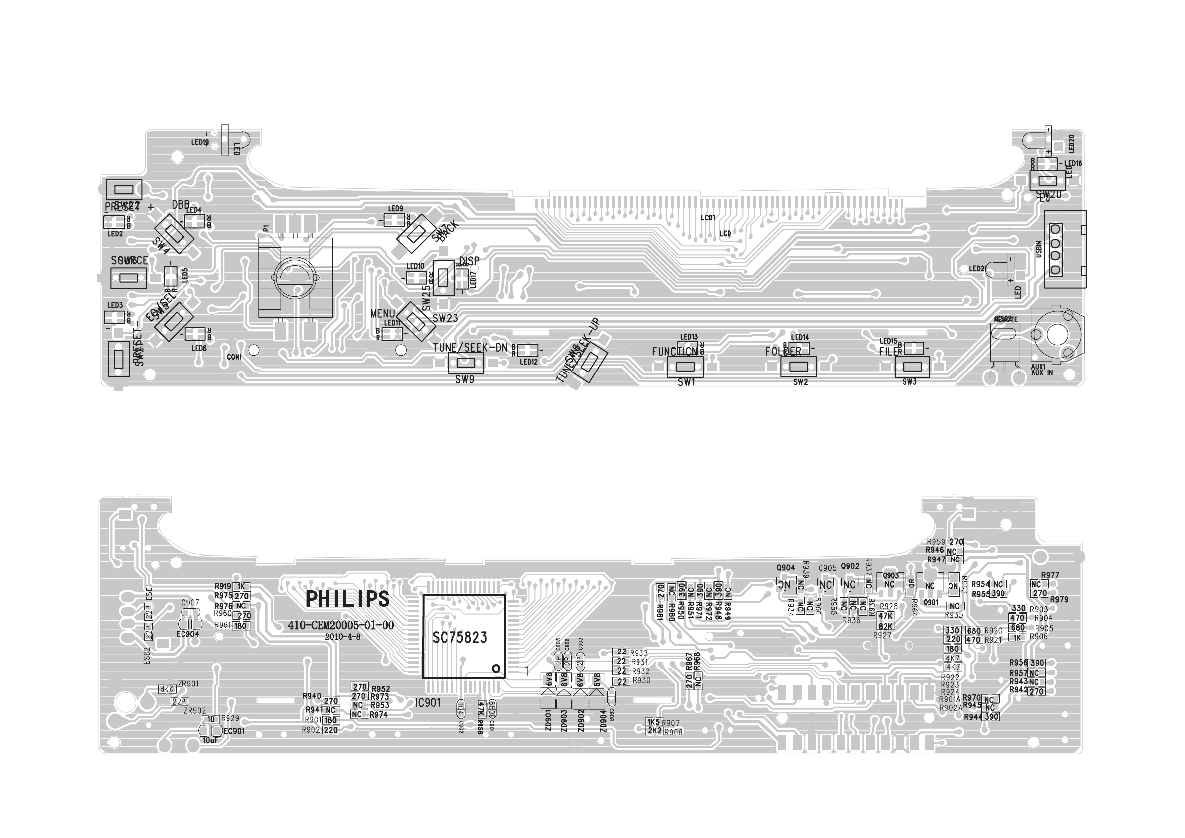
LAYOUT DIAGRAM - PANEL BOARD
6 - 2
6 - 2
Page 18
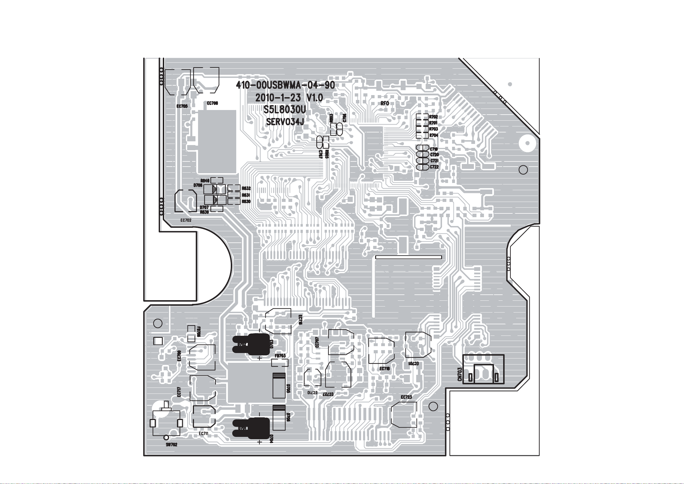
CIRCUIT DIAGRAM - SERVO BOARD
7 - 1
7 - 1
Page 19
LAYOUT DIAGRAM - SERVO BOARD
TOP SIDE VIEW
7 - 2 7 - 2
Page 20
LAYOUT DIAGRAM - SERVO BOARD
BOTTOM SIDE VIEW
7 - 3 7 - 3
Page 21
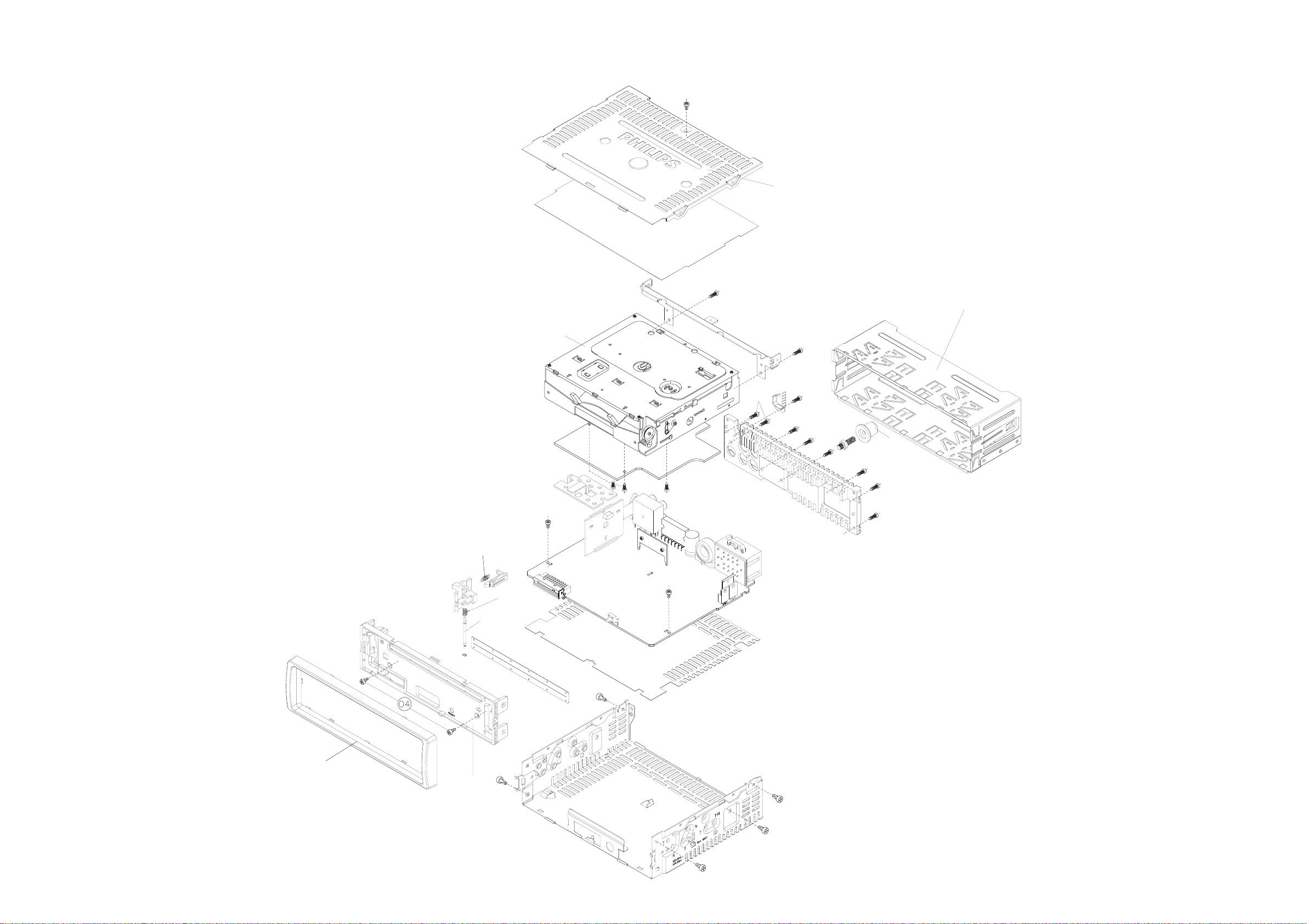
EXPLODED VIEW DIAGRAM
8 - 1 8 - 1
6501
6505
CD01
6503
6504
ASS02
6502
ASS05
PL01
Page 22

Revision list
Version1.0 ( 3141 785 35130)
*Initial Release
Version1.1 ( 3141 785 35131)
*New version 51 added.
9 - 1
Page 23

Trouble shooting
Trouble shooting
Trouble shootingTrouble shooting
Product Model
NO.
1
2
failure
phenomena
NO Power
NO audio
output
CEM2000
Area CEM2000/00
Tate 2011-11-19
failure cause remark
a. To check whether it is connect well of the ISO connector (4 PIN power input ). Whether it is loose of the 15A fuse of the
ISO connector, or insert non in place.
b. To check whether there is any contamination and bad contact on the 22 Pin male/female connector on the panel and main
board.
c. To check the power supply of main board B+ACC should be +12V; The voltage of stabilivolt of ACC power supply circuit
ZD3 (6V8) should be 6V8.
d.To check the voltage of the 17 pin of U1 MCU should be +4V8.
e. To check the voltage of the 15 pin16 pin47 pin of U1 MCU should be +5V; The output voltage of U4 (LM2950) should
be +5V.
f. To check the oscillation frequence of crystal XT4 shuold be 7.2MHz .
g.To check the resistor network of NR1 (4K7).
H. To check the voltage of the15 pin(Lamp Vcc) of CN5 should be 6V4.
a. To check whether the volume knob is turn to the minimum position.
b. To check whether the unit is at MUTE mode, press SOURCE button and check whether it is effective of the input sound
source.
c. To check whether the connection of 8 PIN audio output wire of ISO connector is correct; wrong connection or short circuit
to the ground will caused the protection of the power amplifier( no voltage output).
d . To check the circuit of power amplifier U3 (LV47002) and VOLUME U5(7313 IC).
3
Radio
abnormal
e. To check the normal voltage of 22 PIN(MUTE) of power amplifier U3(LV47002) , normally should be 4V1
f. To check the voltage of 2 pin of audio processor U57313 IC, should be +9V0.
g. To check the voltage of control PIN SDASCLthe 2728 pinof audio processor U57313 IC, should be +4V9.
a. To check the antenna of the tuner.
b. To check whether the strength of then input signal of the tuner is too weak.
c. To check the voltage of the 7 pin22 pin33 pin40 pin41 pin43 pin of the U2 of the tuner IC7703, should be
+5V0.
d. To check the voltage of the 26 pin(SDA) of the tuner IC(7703), should be +3V8; the 27 pin(SCL) should be +4V2.
e. To check the L output voltage of the 37 pin of tuner IC(7703) should be 1V7, the 38 pin R output voltage , should be 1V7.
24
Page 24

NO.
4
failure
phenomena
CD defective
failure cause remark
a. To check whether the signal format of the disc is correspond to the request of the unit, whether there is any
contamination or damage or light leakage on the surface of the disc.
b. To check whether there is any abnormal of the rotation of the deck mechanism, or whether the disc is enter in
position.
c. To check whether it is normal when reading USB?
d. To check whether the 17 P FFC of laser pick up is inserted in place, whether the socket of it is loose.
e. To check whether there is any contamination or foreign body on the surface of the laser pick up.
f. To check the servo board connector of CN702 and main board connector of CN9, whether the socket of it is loose.
j. To check the switch SW702 on the servo board.
h. To check the rotation mechanism of CD deck mechanism.
i. To check whether the rotation belt of deck mechanism is dislocation or loose.
a. To check whether the USB/SD signal format is correspond to the request of the unit.
5
USB/SD
defective
6 AUX defective
b. To check the voltage of the the uppermost pin of the USB connector, should be +5V.
c. To check whether there is any wearing and scratch of the shrapnel and pin of the panel USB.
d.To check the servo board connectors of CN702 and the main board connectors of CN9, whether the socket of it is
loose.
e.To check the servo board connectors of CON707 and the SD/MMC board connectors whether the socket of it is
loose.
f. To check whether there is any contamination and bad contact on the male/female connector of the panel and main
board. If necessary, can exchange the panel to test whether the defective is occurred by the unit or panel.
a. To check the SOURCE should be in MP3-LINK mode.
b. To check the AUX IN input signal.
c. To check whether there is any contamination and bad contact on the male/female connector of the panel and main
board. If necessary, can exchange the panel to test whether the defective is occurred by the unit or panel.
25
Page 25

Princeton Technology Corp.
ANGUS ELECTRONICS CO., LTD
Tel: (852) 2345 0540 Fax: (852) 2345 9948 Web Site: www.angus.com.hk
PT7313E
Stereo Audio Processor for Car Audio
DESCRIPTION
The PT7313E is an audio processor designed for
versatile application, including 3 stereo input selectors
with adjustable gain, master volume control with low
frequency loudness compensation, individual output
attenuator and tone control. It is a good solution for
the car audio signal processing.
Due to the high reliability requirement from the car
audio business, the PT7313E improves both audio
performance and input surge current capability that
make PT7313E the best solution for the cost-effective
car audio systems.
APPLICATIONS
• Car Audio
• Home Audio System
• Powered Speaker System
APPLICATION CIRCUIT
PT7313E
PT2313E
1
2
VDD
3
AGND
4
TREB_ L
TREB_ R
5
RIN
6
ROU T
7
LOUD _R
8
RIN3
9
RIN2
10
RIN1
11
LOU D_ L
12
LIN3
13
LIN2 LIN 1
14 1 5
AUDIO 3
AUDIO 2
AUDIO 1
Input Surge
Protection
L
R
L
R
L
R
2.2K
2.2K
2.2K
2.2K
2.2K
2.2K
2.2uF
2.2uF
2.2uF
2.2uF
2.2uF
2.2uF
22uF
VDD
2.7n
2.7n
2.2uF
100n
100n
FEATURES
• 3 stereo inputs with gain selection, range from 0dB
to +11.25dB in 3.75dB/step
• Master volume from 0 dB to -78.75dB in
1.25dB/step
• Speaker attenuator for balance and fader, range
from 0dB to -38.75dB in 1.25dB/step
• Each channel output can be muted individually.
• Low frequency loudness compensation
LFOUT
RFOU T
LROUT
RROU T
BOUT_R
BOUT_L
• Bass and Treble control, range from -14dB to
+14dB in 2dB/step
• Wide operation range (VDD = 4V to 10V)
28REF
SCL
SDA
DGND
BIN_R
BIN_L
LOUT
LIN
16
27
26
25
24
23
22
21
20
19
18
17
100n
100n
100n
100n
2.2uF
MCU
10uF
10uF
10uF
10uF
5.6K
5.6K
Front Left
Front Right
Rear Left
Rear Right
Power
Amplifier
V1.0 1 February 2010
Page 26

G
G
e
S
Princeton Technology Corp.
BLOCK DIAGRAM
ANGUS ELECTRONICS CO., LTD
Tel: (852) 2345 0540 Fax: (852) 2345 9948 Web Site: www.angus.com.hk
Speaker Attenuator
PT7313E
With Mute
LROUT
LFOUT
TREB_L
BIN_L
BOUT_L
LOUD_L
LIN
LOUT
LIN1
LIN2
TREBLE
BASS
LOUDNE SS
Input SW and
AIN
REF
REF
REF
Master
Volume
Loud
W
REF
REF
REF
Input SW and
AIN
TREBLE
BASS
LOUDN ESS
RROUT
RFOUT
TREB_R
BIN_R
BOUT_R
LOUD_R
RIN
ROUT
RIN1
RIN2
LIN3
VDD
REF
AGND
REF
INT
R
f
REF
BIAS
I2C
DECODER
RIN3
REF
SCL
SDA
DGND
V1.0 2 February 2010
Page 27

ANGUS ELECTRONICS CO., LTD
Tel: (852) 2345 0540 Fax: (852) 2345 9948 Web Site: www.angus.com.hk
Princeton Technology Corp.
ORDER INFORMATION
Valid Part Number Package Type Top Code
PT7313E-S 28 Pins, SOP, 300mil PT7313E
PIN CONFIGURATION
PT7313E
VDD
AGND
TREB_ L
TREB_ R
RIN
ROU T
1
2
3
4
5
6
7
28REF
27
26
25
24
23
22
PT7313E
LOUD_ R
RIN3
RIN2
RIN1
LOUD_ L
8
9
10
11
12
13
LIN3
14 15
LIN2 LIN1
21
20
19
18
17
16
SCL
SDA
DGND
LFOUT
RFOU T
LROUT
RROU T
BOUT_R
BIN_R
BOUT_L
BIN_L
LOUT
LIN
V1.0 3 February 2010
Page 28

ANGUS ELECTRONICS CO., LTD
Tel: (852) 2345 0540 Fax: (852) 2345 9948 Web Site: www.angus.com.hk
Princeton Technology Corp.
PIN DESCRIPTION
Pin Name I/O Description Pin No.
REF - Analog reference voltage (1/2VDD) 1
VDD - Supply input voltage 2
AGND - Analog ground 3
TREB_L I Left channel input for treble controller 4
TREB_R I Right channel input for treble controller 5
RIN I Right channel volume controller input 6
ROUT O Right channel Input selector output 7
LOUD_R I Right channel loudness input 8
RIN3 I Right channel input 3 9
RIN2 I Right channel input 2 10
RIN1 I Right channel input 1 11
LOUD_L I Left channel loudness input 12
LIN3 I Left channel input 3 13
LIN2 I Left channel input 2 14
LIN1 I Left channel input 1 15
LIN I Left channel volume controller input 16
LOUT O Left channel Input selector output 17
BIN_L I Left channel input for bass controller 18
BOUT_L O Left channel output for bass controller 19
BIN_R I Right channel input for bass controller 20
BOUT_R O Right channel output for bass controller 21
RROUT O Right rear speaker output 22
LROUT O Left rear speaker output 23
RFOUT O Right front speaker output 24
LFOUT O Left front speaker output 25
DGND - Digital ground 26
SDA I I2C data input 27
SCL I I2C clock input 28
PT7313E
V1.0 4 February 2010
Page 29

ANGUS ELECTRONICS CO., LTD
Tel: (852) 2345 0540 Fax: (852) 2345 9948 Web Site: www.angus.com.hk
Princeton Technology Corp.
CONTROL BUS SPECIFICATION
BUS INTERFACE
PT7313E
All functions of the PT7313E are controlled by the I2C interface, the interface is consisting by SDA and SCL pins. Detail
protocol of the I
the PT7313E positive supply voltage may required in some application especially the MCU output high level is no
enough.
2
C bus will discuss on the next section. It should be noted that the bus level pull-up resistors connected to
DATA VALIDITY
A data on the SDA Line is considered valid and stable only when the SCL Signal is in HIGH State. The HIGH and LOW
State of the SDA Line can only change when the SCL signal is LOW. Please refer to the figure below.
START AND STOP CONDITIONS
A Start Condition is activated when
1) The SCL is set to HIGH and
2) SDA shifts from HIGH to LOW State.
The Stop Condition is activated when
1) SCL is set to HIGH and
2) SDA shifts from LOW to HIGH State. Please refer to the timing diagram below..
BYTE FORMAT
Every byte transmitted to the SDA Line consists of 8 bits. Each byte must be followed by an Acknowledge Bit. The MSB
is first transmitted.
V1.0 5 February 2010
Page 30

Princeton Technology Corp.
ACKNOWLEDGE
ANGUS ELECTRONICS CO., LTD
Tel: (852) 2345 0540 Fax: (852) 2345 9948 Web Site: www.angus.com.hk
PT7313E
During the Acknowledge clock pulse (ACK), the SDA output port of the master device (μP) would be sets on Hi-Z state,
if peripheral device (ex : audio processor) recognize the I
during the SCL clock pulse held in HIGH state period. Please refer to the diagram below. The slave device that has been
addressed to generate an Acknowledge after receiving each byte, otherwise, the SDA Line will remain at the High level
in period of the ninth (9th) clock pulse. In this case, the host controller will generate a STOP sign in order to abort the
transfer mission.
2
C command the SDA line will be pull-down by slave device
TRANSMISSION WITHOUT ACKNOWLEDGE
If the application does not need to verify the Acknowledge signal that generated by the slave device is right or not, host
controller can just bypass the acknowledge check and transmit next data byte to the slave device. If this approach is
used, there are greater chances of faulty operation as well as decrease in noise immunity.
INTERFACE PROTOCOL
The interface protocol sequence was defined in below section:
• A Start sign
• A Chip Address of the desire slave device. The W Bit must be “0” (written). The PT7313E will always response an
Acknowledge on the end of each byte.
• A Data Sequence (N-Bytes + Acknowledge)
• A Stop Condition
PT7313E Address
MSB First Byte LSB MSB LSB MSB LSB
START 1 0 0 0 1 0 0 W ACK DATA ACK DATA ACK STOP
Chip Address Data Transmitting (N-Bytes + Acknowledge)
ACK=Acknowledge
PT7313E CHIP ADDRESS
The PT7313E chip address is 88H AND binary table is shown on below.
MSB LSB
1 0 0 0 1 0 0 0
V1.0 6 February 2010
Page 31

Princeton Technology Corp.
DATA BYTES
MSB LSB Function
0 0 B2 B1 B0 A2 A1 A0 Master Volume
1 1 0 B1 B0 A2 A1 A0 Speaker ATT LR
1 1 1 B1 B0 A2 A1 A0 Speaker ATT RR
1 0 0 B1 B0 A2 A1 A0 Speaker ATT LF
1 0 1 B1 B0 A2 A1 A0 Speaker ATT RF
0 1 0 G1 G0 LD S1 S0 Input Switch and Gain
0 1 1 0 C3 C2 C1 C0 Bass Control
0 1 1 1 C3 C2 C1 C0 Treble Control
DATA RATE
ANGUS ELECTRONICS CO., LTD
Tel: (852) 2345 0540 Fax: (852) 2345 9948 Web Site: www.angus.com.hk
PT7313E
The PT7313E support Standard-Mode (100kbit/s) I2C data rate In all operation condition, in specified condition it also
support Fast-Mode (400kbit/s) I
MCU Level
2.5V F F x x x x x
3.3V F F F F S S x
5V x F F F F F F
Notes:
1. x = Not allow in this combination; S = Standard Mode Supported, F = Fast Mode Supported.
2. Data rate specification is design guarantee only, not fully tested in every combination.
2
C data rate, please refer to the follow table:
PT7313E VDD Voltage
4V 5V 6V 7V 8V 9V 10V
I2C BUS INITIAL TIME
The PT7313E is controlled by the I2C bus command; each time the supply voltage applied to chip it needs an initial time
to reset all of the internal decoder register, in this period access the I
by capacitance it attached on REF pin (CREF) and Td. For proper operation USER must check the I
this requirement and recommended Td timing shown on next page is 50mS.
POWER ON
VDD
90% VREF
2
C bus is prohibited. The initial time is determinate
2
C starts timing is fit
VREF
I2C PR OHIBIT Td
50mS
I2C STAR T S
I2C
V1.0 7 February 2010
Page 32

ANGUS ELECTRONICS CO., LTD
Tel: (852) 2345 0540 Fax: (852) 2345 9948 Web Site: www.angus.com.hk
Princeton Technology Corp.
FUNCTION DESCRIPTION
MASTER VOLUME
The table below gives a detailed description of the Master Volume Data Bytes. For example, a volume of -37.5dB is given
by 0 0 0 1 1 1 1 0.
MSB LSB Function
0 0 B2 B1 B0 A2 A1 A0 1.25dB/step
0 0 0 0
0 0 1 -1.25
0 1 0 -2.5
0 1 1 -3.75
1 0 0 -5
1 0 1 -6.25
1 1 0 -7.5
1 1 1 -8.75
0 0 B2 B1 B0 A2 A1 A0 10dB/step
0 0 0 0
0 0 1 -10
0 1 0 -20
0 1 1 -30
1 0 0 -40
1 0 1 -50
1 1 0 -60
1 1 1 -70
PT7313E
SPEAKER ATTENUATORS
The speaker attenuator in most of car audio system is performs balance and fader function, the table below gives a
detailed description of the speaker attenuators data bytes. Total control range of the speaker attenuator is from 0dB to
-37.5dB.
Example 1, an attenuation gain of -6.25dB on the Speaker Right Rear channel is combined 0dB and -6.25dB, therefore
it should be given by: 1 1 1 0 0 1 0 1.
Example 2, an attenuation gain of -32.5dB on the Speaker Left Front channel is combined -30dB and -2.5dB, therefore it
should be given by: 1 0 0 1 1 0 1 0.
MSB LSB Function
1 0 0 B1 B0 A2 A1 A0 Speaker LF
1 0 1 B1 B0 A2 A1 A0 Speaker RF
1 1 0 B1 B0 A2 A1 A0 Speaker LR
1 1 1 B1 B0 A2 A1 A0 Speaker RR
0 0 0 0
0 0 1 -1.25
0 1 0 -2.5
0 1 1 -3.75
1 0 0 -5
1 0 1 -6.25
1 1 0 -7.5
1 1 1 -8.75
0 0 0
0 1 -10
1 0 -20
1 1 -30
1 1 1 1 1 Mute
V1.0 8 February 2010
Page 33

ANGUS ELECTRONICS CO., LTD
Tel: (852) 2345 0540 Fax: (852) 2345 9948 Web Site: www.angus.com.hk
Princeton Technology Corp.
INPUT SELECTOR
The PT7313E provides 3 stereo input selector and following table shows the definition of the correspond register. The LD
register is determinate the loudness function is ON or OFF, and G0 and G1 determinate the input gain of the selector
output, this function is use to matching level of different sources to avoid overall volume difference.
MSB LSB Function
0 1 0 G1 G0 LD S1 S0 Audio switch
0 0 Stereo 1
0 1 Stereo 2
1 0 Stereo 3
0 Loudness ON
1 Loudness OFF
0 0 +11.25dB
0 1 +7.5dB
1 0 +3.75dB
1 1 0dB
BASS AND TREBLE DATA BYTES
The following table shows a detailed description of the Bass and Treble Data Byte. For example a Treble at -12dB is
given by: 0 1 1 1 0 0 0 1 (0x71).
MSB LSB Function
0 1 1 0 C3 C2 C1 C0 Bass
0 1 1 1 C3 C2 C1 C0 Treble
0 0 0 0 -14dB
0 0 0 1 -12dB
0 0 1 0 -10dB
0 0 1 1 -8dB
0 1 0 0 -6 dB
0 1 0 1 -4 dB
0 1 1 0 -2 dB
0 1 1 1 0 dB
1 1 1 1 0 dB
1 1 1 0 +2 dB
1 1 0 1 +4 dB
1 1 0 0 +6 dB
1 0 1 1 +8 dB
1 0 1 0 +10 dB
1 0 0 1 +12 dB
1 0 0 0 +14 dB
PT7313E
V1.0 9 February 2010
Page 34

ANGUS ELECTRONICS CO., LTD
Tel: (852) 2345 0540 Fax: (852) 2345 9948 Web Site: www.angus.com.hk
Princeton Technology Corp.
TUNNING TONE CURVE CHARACTERISTICS
The tone control response character is possible tuned to match user’s wishes, please refer to following chart to realize
the characteristics between the different component values.
For the reasons to achieve low distortion and precision response gain, using high quality low tolerance X7R SMD
capacitor on tone circuit is recommended.
The loudness boost gain is adaptive with the master volume attenuation setting, more attenuation means more low
frequency boost, in the maximum volume the loudness boost will return to flat response.
PT7313E
+16
+14
+12
+10
+8
d
B
A
+6
g
+4
+2
+0
-2
-4
-6
10 20k20 50 100 200 500 1k 2k 5k
68nF
100nF
150nF
Hz
+16
+14
+12
+10
d
B
g
A
+8
+6
+4
+2
+0
-2
-4
-6
10 50k20 50 100 200 500 1k 2k 5k 10k 20k
2.7nF
1.5nF
1nF
Hz
PT7313E Bass Response VS CAP PT7313E Treble Response VS CAP
-10
-15
56nF
-20
-25
d
-30
B
V
-35
-40
-45
-50
10 20k20 50 100 200 500 1k 2k 5k
Hz
100nF
220nF
OPEN
+0
-10
-20
d
-30
B
g
-40
A
-50
-60
-70
-80
20 20k50 100 200 500 1k 2k 5k 10k
Hz
PT7313E Loudness Response VS CAP
(VOLUME=-40dB)
PT7313E Loudness Response VS Master Volume
V1.0 10 February 2010
Page 35

ANGUS ELECTRONICS CO., LTD
Tel: (852) 2345 0540 Fax: (852) 2345 9948 Web Site: www.angus.com.hk
Princeton Technology Corp.
ABSOLUTE MAXIMUM RATINGS
Parameter Symbol Min. Max. Unit
Operating supply voltage VDD - 10 V
Latch up current Iin -100 +100 mA
ESD grade
Input voltage Vin -0.3 VDD+0.3 V
Operating temperature Topr -40 +85 ℃
Storage temperature Tstg -65 +150 ℃
Human body model HBM -2 +2 KV
Machine model MM -0.2 +0.2 KV
QUICK REFERENCE DATA
Parameter Symbol Min. Typ. Max. Unit
Supply voltage VDD 4 9 10 V
Max. input signal handling VCL 2.3 2.6 - Vrms
Total harmonic distortion (1Vrms,1KHz) THD - 0.03 0.07 %
Signal To noise ratio S/N - 100 - dBV
Channel separation (f=1KHz) Sc - 100 - dB
Volume control 1.25dB step - -78.75 - 0 dB
Bass & treble control 2dB step - -14 - +14 dB
Balance control 1.25dB step - -37.5 - 0 dB
Input gain 3.75dB step - 0 - 11.25 dB
Mute attenuation - - 100 - dB
PT7313E
V1.0 11 February 2010
Page 36

x
x
t
V
X
X
ANGUS ELECTRONICS CO., LTD
Tel: (852) 2345 0540 Fax: (852) 2345 9948 Web Site: www.angus.com.hk
Princeton Technology Corp.
ELECTRICAL CHARACTERISTICS
Unless otherwise specified: Ta=25℃, VDD=9V, RL=100KΩ, Rg=20Ω, all controls flat, F=1KHz, and all of peripheral
components according to standard application circuit.
Parameter Symbol Test Condition Min. Typ. Max. Unit
Power Supply
Supply voltage VDD - 5 9 10 V
Supply current Is
Input Selectors
Input resistance RIN Input 1, 2, 3 35 50 70 KΩ
Max. input level V
Input separation ISIN F=20 ~ 20KHz 90 100 - dB
Min. input gain G
Max. input gain G
Step resolution G
Gain set error EA - -1 0 1 dB
Minimum load RL Vo=2Vrms, LOUT, ROUT 5 - DC offset V
olume Control
Input resistance RIN VOL=0dB 13 20 27 KΩ
Min. attenuation A
Max. attenuation A
Step resolution A
Attenuation set error EA VOL=0 ~ -70dB -1 0 1 dB
Speaker Attenuators
Max. Gain A
Max. attenuation A
Step resolution S
Attenuation set error EA - -1 0 1 dB
Output mute attenuation A
DC offset V
Bass Control
Control range Gb Max. Boost/Cut ±12 ±14 ±16 dB
Step resolution B
Feedback resistance RB - 34 44 58 KΩ
Treble Control
Control range Gt Max. Boost/Cut ±12 ±14 ±16 dB
Step resolution T
Loudness Control
Boost gain GLD Volume=-40dB, F=20Hz 18 20 22 dB
Audio Outputs
Max. output level V
DC voltage level V
Minimum load RL - 5 - - KΩ
General
Signal to noise ratio SNR
Distortion THD
Channel separation Cs L to R or R to L channel 90 100 - dB
I2C crosstalk Ct I2C to audio output - 90 - dB
Ripple rejection PSRR CREF=22µF, F=100Hz - 75 - dB
I2C Bus
Input low voltage VIL VDD=9V - - 1 V
Input high voltage VIH VDD=9V 3 - - V
Input current IIN - -5 - +5 µA
SDA pull down voltage Vack Rpull up=3K, ACK=active - 0.4 - V
All Gain=0dB; THD=1% 2.3 2.6 - Vrms
ima
- -1 0 1 dB
INmin
- 10.5 11.25 12 dB
INma
- - 3.75 - dB
INs
0dB to +11.25dB - 3 10 mV
DCO
- -1 0 1 dB
VMIN
- -75 -78.75 -82 dB
VMA
- 1.15 1.25 1.3 dB
STEP
- -1 0 +1 dB
VMIN
- -36 -37.5 -39 dB
VMA
- 1.15 1.25 1.35 dB
STEP
- - 100 - dB
MUTE
0dB to MUTE - 5 10 mV
DCO
- 1.7 2 2.3 dB
STEP
- 1.7 2 2.3 dB
STEP
THD=1% 2.3 2.6 - Vrms
OMAX
- 0.49 0.5 0.51 VDD
OUT
All Gain=0dB, A-weighted - 100 -
All Gains=0dB, Muted - 100 -
All Gain=0, Vin=1Vrms - 0.03 0.07
All Gain=0, Vin=100Vrms - 0.01 0.03
PT7313E
VDD=9V - 30 40
VDD=5V - 25 32
mA
KΩ
dBV
%
V1.0 12 February 2010
Page 37

Princeton Technology Corp.
+16
+12
+8
d
B
g
A
+4
+0
-4
-8
ANGUS ELECTRONICS CO., LTD
Tel: (852) 2345 0540 Fax: (852) 2345 9948 Web Site: www.angus.com.hk
PT7313E
+16
+12
+8
d
B
g
A
+4
+0
-4
-8
-12
-16
20 30k50 100 200 500 1k 2k 5k 10k
Hz
-12
-16
20 30k50 100 200 500 1k 2k 5k 10k
Hz
Bass Response Treble Response
-70
-80
-90
d
-100
B
d
B
r
-110
-120
-130
20 30k50 100 200 500 1k 2k 5k 10k
Hz
A
-20
-40
Cref=22µF
-60
-80
-100
-120
20 20k50 100 200 500 1k 2k 5k
Hz
2 Channel Crosstalk PSRR
20
10
5
2
1
0.5
%
0.2
0.1
0.05
0.02
0.01
0.003
1m 42m 5m 10m 20m 50m 200m 500m 1 2
(RL=10KΩ)
4V
5V
8V
9V
10V
d
B
V
V
-50
-60
-70
L1 to L2
-80
-90
-100
-110
20 20k50 100 200 500 1k 2k 5k
Hz
Output THD VS VDD Voltage Input Selector Separation
V1.0 13 February 2010
Page 38

O
l
(V)
Princeton Technology Corp.
4.5
4
3.5
3
2.5
2
1.5
1
0.5
Maximum output voltage (V)
0
3456789101112
Supply Voltage (V)
Maximum Output Level (RL=100KΩ) Supply Current VS VDD
Maximum output voltage
3.5
3
2.5
2
tage
1.5
1
utput vo
0.5
ANGUS ELECTRONICS CO., LTD
Tel: (852) 2345 0540 Fax: (852) 2345 9948 Web Site: www.angus.com.hk
PT7313E
45
40
35
30
25
20
15
Operation Current (mA )
10
3456789101112
16
14
12
10
8
Output Noise (uV)
6
Supply Voltage (V)
80KHz LPF
20-20KHz
A-weighted
0
110100
4
3456789101112
Load (Kohm)
Maximum Output Level VS R
0
-10
-20
-30
-40
-50
-60
Measurement (dB)
-70
-80
Residual Noise
LOAD
0
-10
-20
-30
-40
-50
-60
-70
-80
Measurement (dB)
-90
-100
-110
-80-70-60-50-40-30-20-100
Volume attenuate level (dB)
Volume Attenuation Speaker Attenuation
Supply Voltage (V)
-40-30-20-100
Speaker attenuate level (dB)
V1.0 14 February 2010
Page 39

ANGUS ELECTRONICS CO., LTD
Tel: (852) 2345 0540 Fax: (852) 2345 9948 Web Site: www.angus.com.hk
Princeton Technology Corp.
PACKAGE INFORMATION
28-PIN, SOP, 300MIL
PT7313E
Symbol Min. Nom. Max.
A - - 2.65
A1 0.10 - 0.30
b 0.31 - 0.51
c 0.20 - 0.33
D 17.90 BSC
E 10.30 BSC
E1 7.50 BSC
e 1.27 BSC
L 0.38 - 1.27
θ 0° - 8°
Notes:
1. Refer to JEDEC MS-013 AE
2. All Dimensions are in millimeter.
V1.0 15 February 2010
Page 40

ANGUS ELECTRONICS CO., LTD
Tel: (852) 2345 0540 Fax: (852) 2345 9948 Web Site: www.angus.com.hk
Princeton Technology Corp.
IMPORTANT NOTICE
Princeton Technology Corporation (PTC) reserves the right to make corrections, modifications, enhancements,
improvements, and other changes to its products and to discontinue any product without notice at any time.
PTC cannot assume responsibility for use of any circuitry other than circuitry entirely embodied in a PTC product. No
circuit patent licenses are implied.
PT7313E
V1.0 16 February 2010
Page 41

TDA7388
Fi
4 X 41W QUAD BRIDGE CAR RADIO AMPLIFIER
1 FEATURES
■ HIGH OUTPUT POWER CAPABILITY:
■ 4 x 41W/4Ω MAX.
■ 4 x 25W/4Ω @ 14.4V, 1KHz, 10%
■ LOW DISTORTION
■ LOW OUTPUT NOISE
■ ST-BY FUNCTION
■ MUTE FUNCTION
■ AUTOMUTE AT MIN. SUPPLY VOLTAGE
DETECTION
■ LOW EXTERNAL COMPONENT COUNT:
– INTERNALLY FIXED GAIN (26dB)
– NO EXTERNAL COMPENSATION
– NO BOOTSTRAP CAPACITORS
2 PROTECTIONS:
■ OUTPUT SHORT CIRCUIT TO GND, TO V
ACROSS THE LOAD
■ VERY INDUCTIVE LOADS
■
OVERRATING CHIP TEMPERATURE WITH
SOFT THERMAL LIMITER
■ LOAD DUMP VOLTAGE
■
FORTUITOUS OPEN GND
gure 1. Package
Flexiwatt25
Table 1. Order Codes
Part Number Package
TDA7388 Flexiwatt25
■
REVERSED BATTERY
■ ESD
3 DESCRIPTION
The TDA7388 is a new technology class AB Audio
Power Amplifier in Flexiwatt 25 package designed
for high end car radio applications.
,
S
Thanks to the fully complementary PNP/NPN output configuration the TDA7388 allows a rail to rail
output voltage swing with no need of bootstrap capacitors. The extremely reduced components
count allows very compact sets.
Figure 2. Block and Application Diagram
Vcc1 Vcc2
ST-BY
MUTE
IN1
0.1µF
IN2
0.1µF
IN3
0.1µF
IN4
0.1µF
AC-GND
0.47µF47µF
July 2005
SVR TAB S-GND
N.C.
OUT1+
OUT1-
PW-GND
OUT2+
OUT2-
PW-GND
OUT3+
OUT3-
PW-GND
OUT4+
OUT4-
PW-GND
D99AU1018
100nF470µF
Rev. 1
1/10
Page 42

TDA7388
Table 2. Absolute Maximum Ratings
Symbol Parameter Value Unit
V
V
CC (DC)
V
CC (pk)
I
CC
O
Operating Supply Voltage 18 V
DC Supply Voltage 28 V
Peak Supply Voltage (t = 50ms) 50 V
Output Peak Current:
Repetitive (Duty Cycle 10% at f = 10Hz)
Non Repetitive (t = 100µs)
P
tot
T
j
T
stg
Power dissipation, (T
Junction Temperature 150 °C
Storage Temperature – 55 to 150 °C
Figure 3. Pin Connection
4.5
5.5
= 70°C) 80 W
case
A
A
1 25
TAB
OUT2-
P-GND2
ST-BY
CC
V
OUT2+
OUT1-
OUT1+
P-GND1
SVR
IN1
IN2
IN4
S-GND
IN3
OUT3+
AC-GND
OUT3-
P-GND3
CC
V
MUTE
OUT4+
D94AU159A
OUT4-
HSD
P-GND4
Table 3. Thermal Data
Symbol Parameter Value Unit
Thermal Resistance Junction to Case max 1 °C/W
2/10
R
th j-amb
Page 43

TDA7388
Table 4. Electrical Characteristcs (VS = 14.4V; f = 1KHz; Rg = 600Ω; RL = 4Ω;T
= 25°C; Refer to the
amb
Test and application diagram, unless otherwise specified.)
Symbol Parameter Test Condition Min. Typ. Max. Unit
I
q1
V
OS
∆V
OS
G
P
P
o max
THD Distortion P
e
No
SVR Supply Voltage Rejection f = 100Hz; V
f
ch
R
C
Quiescent Current
RL = ∞
120 190 350 mA
Output Offset Voltage Play Mode ±80 mV
During Mute ON/OFF Output
Offset Voltage
Voltage Gain 25 26 27 dB
v
Output Power THD = 10%; VS = 14.4V 22 26 W
o
Max.Output Power (*) VS = 14.4V 38 41 W
= 4W 0.04 0.15 %
o
Output Noise "A" Weighted 50 70 µV
Bw = 20Hz to 20KHz 70 100 µV
= 1V
r
rms
50 65 dB
High Cut-Off Frequency Po = 0.5W 100 200 KHz
Input Impedance 70 100 KΩ
i
Cross Talk f = 1KHz; Po = 4W 60 70 dB
T
f = 10KHz; Po = 4W 50 60 dB
±80 mV
St-By Current Consumption 50 µA
St-By OUT Threshold
V
SB out
I
SB
Voltage
V
SB IN
A
M
V
M out
V
M in
V
AM in
I
pin22
(*) Saturated square wave output.
(
St-By IN Threshold Voltage (Amp: OFF) 1.5 V
Mute Attenuation P
Mute OUT Threshold Voltage (Amp: Play) 3.5 V
Mute IN Threshold Voltage (Amp: Mute) 1.5 V
VS Automute Threshold (Amp: Mute); Att ≥ 80dB; P
Muting Pin Current V
(Amp: ON) 3.5 V
= 4W 80 90 dB
Oref
6.5
8.5
(Amp: Play); Att < 0.1dB; P
= 1.5V
MUTE
= 4Ω
Oref
= 0.5Ω
O
7.6
51120µA
(Source Current)
V
V
3/10
Page 44

TDA7388
Figure 4. Standard Test and Application Circuit
ST-BY
MUTE
IN1
IN2
IN3
IN4
R1
10K
R2
47K
C1
0.1µF
C2 0.1µF
C3 0.1µF
C4 0.1µF
C9
1µF
C10
1µF
S-GND
C8
0.1µF
4
22
11
12
15
14
13
16 10 25 1
C5
0.47µF
C7
2200µF
Vcc1-2
SVR TAB
C6
47µF
Vcc3-4
620
9
8
7
5
2
3
17
18
19
21
24
23
HSD
OUT1
OUT2
OUT3
OUT4
D95AU335B
4/10
Page 45

4 P.C.B. AND COMPONENT LAYOUT OF THE FIGURE 4
Figure 5. Components & Top Copper Layer
TDA7388
Figure 6. Bottom Copper Layer
5/10
Page 46

TDA7388
Figure 7. Quiescent Current vs. Supply Voltage
Figure 8. Quiescent Output Voltage Supply
Voltage
Figure 10. Distortion vs. Output Power
Figure 11. Distortion vs. Frequency
Figure 9. Output Power vs. Supply Voltage
6/10
Figure 12. Supply Voltage Rejection vs.
Frequency.
Page 47

TDA7388
Figure 13. Output Noise vs. Source
Resistance.
Figure 14. Power Dissipation & Efficiency vs.
Output Power.
5 APPLICATION HINTS
(ref. to the circuit of fig. 4)
5.1 SVR
Besides its contribution to the ripple rejection, the SVR capacitor governs the turn ON/OFF time sequence
and, consequently, plays an essential role in the pop optimization during ON/OFF transients. To conveniently serve both needs, ITS MINIMUM RECOMMENDED VALUE IS 10µF.
5.2 INPUT STAGE
The TDA7388’S inputs are ground-compatible and can stand very high input signals (± 8Vpk) without any
performances degradation. If the standard value for the input capacitors (0.1µF) is adopted, the low fre-
quency cut-off will amount to 16 Hz.
5.3 STAND-BY AND MUTING
STAND-BY and MUTING facilities are both CMOS-COMPATIBLE. If unused, a straight connection to Vs
of their respective pins would be admissible.
Conventional/low-power transistors can be employed to drive muting and stand-by pins in absence of true
CMOS ports or microprocessors. R-C cells have always to be used in order to smooth down the transitions
for preventing any audible transient noises.
Since a DC current of about 10 µA normally flows out of pin 22, the maximum allowable muting-series re-
sistance (R2) is 70KΩ, which is sufficiently high to permit a muting capacitor reasonably small (about 1µF).
If R
is higher than recommended, the involved risk will be that the voltage at pin 22 may rise to above the
2
1.5 V threshold voltage and the device will consequently fail to turn OFF when the mute line is brought
down. About the stand-by, the time constant to be assigned in order to obtain a virtually pop-free transition
has to be slower than 2.5V/ms.
7/10
Page 48

TDA7388
Figure 15. Flexiwatt 25 Mechanical Data & Package Dimensions
DIM.
mm inch
MIN. TYP. MAX. MIN. TYP. MAX.
A 4.45 4.50 4.65 0.175 0.177 0.183
B 1.80 1.90 2.00 0.070 0.074 0.079
C 1.40 0.055
D 0.75 0.90 1.05 0.029 0.035 0.041
E 0.37 0.39 0.42 0.014 0.015 0.016
F (1) 0.57 0.022
G 0.80 1.00 1.20 0.031 0.040 0.047
G1 23.75 24.00 24.25 0.935 0.945 0.955
H (2) 28.90 29.23 29.30 1.139 1.150 1.153
H1 17.00 0.669
H2 12.80 0.503
H3 0.80 0.031
L (2) 22.07 22.47 22.87 0.869 0.884 0.904
L1 18.57 18.97 19.37 0.731 0.747 0.762
L2 (2) 15.50 15.70 15.90 0.610 0.618 0.626
L3 7.70 7.85 7.95 0.303 0.309 0.313
L4 5 0.197
L5 3.5 0.138
M 3.70 4.00 4.30 0.145 0.157 0.169
M1 3.60 4.00 4.40 0.142 0.157 0.173
N 2.20 0.086
O 2 0.079
R 1.70 0.067
R1 0.5 0.02
R2 0.3 0.12
R3 1.25 0.049
R4 0.50 0.019
V5˚ (Tp.)
V1 3˚ (Typ.)
V2 20˚ (Typ.)
V3 45˚ (Typ.)
(1): dam-bar protusion not included
(2): molding protusion included
OUTLINE AND
MECHANICAL DATA
Flexiwatt25 (vertical)
V
C
B
V2
V
A
V1
R2
R
L
L1
V1
R2
FLEX25ME
R1
L5
R1 R1
M
D
E
M1
H
V3
H3
OL3 L4
L2
Pin 1
G
H1
G1
H2
R3
R4
N
F
7034862
8/10
Page 49

6 REVISION HISTORY
Table 5. Revision History
Date Revision Description of Changes
July 2005 1 First Issue
TDA7388
9/10
Page 50

TDA7388
Information furnished is believed to be accurate and reliable. However, STMicroelectronics assumes no responsibility for the consequences
of use of such information nor for any infringement of patents or other rights of third parties which may result from its use. No license is granted
by implication or otherwise under any patent or patent rights of STMicroelectronics. Specifications mentioned in this publication are subject
to change without notice. This publication supersedes and replaces all information previously supplied. STMicroelectronics products are not
authorized for use as critical components in life support devices or systems without express written approval of STMicroelectronics.
The ST logo is a registered trademark of STMicroelectronics.
All other names are the property of their respective owners
© 2005 STMicroelectronics - All rights reserved
Australia - Belgium - Brazil - Canada - China - Czech Republic - Finland - France - Germany - Hong Kong - India - Israel - Italy - Japan -
Malaysia - Malta - Morocco - Singapore - Spain - Sweden - Switzerland - United Kingdom - United States of America
STMicroelectronics group of companies
www.st.com
10/10
Page 51

TDA7703/TDA7703R
Highly Integrated Tuner for AM/FM-Carradio
TARGET DESIGN SPECIFICATION
MAIN FEATURES
FULLY INTEGRATED VCO FOR WORLD TUNING
HIGH PERFORMANCE PLL FOR FAST RDS SYSTEM
AM/FM MIXERS WITH HIGH IMAGE REJECTION
INTEGRATED AM-LNA AND AM-PINDIODE
AUTOMATIC SELF ALIGNMENT FOR IMAGE REJECTION
INTEGRATED IF-FILTERS WITH HIGH SELECTIVITY, DYNAMIC RANGE AND
ADAPTIVE BANDWIDTH CONTROL
DIGITAL IF SIGNAL PROCESSING WITH HIGH PERFORMANCE AND FREE OF
DRIFT
HIGH PERFORMANCE STEREODECODER
2
C BUS CONTROLLED
I
SINGLE 5V SUPPLY
SINGLE QFP44 PACKAGE
RDS DEMODULATION WITH GROUP AND BLOCK SYNCHRONIZATION (TDA7703R
ONLY)
Part number Package Packing
TDA7703 LQFP44 (10x10x1.4 mm)
TDA7703R LQFP44 (10x10x1.4 mm)
Tray
LQFP44
6.Jan.09 Rev. 1.0 1/22
Page 52

1.0 DESCRIPTION
The TDA7703/TDA7703R, a.k.a. HIT44,
belong to the HIT (Highly Integrated Tuner)
family, a new generation of high performance
tuners for carradio applications.
They contain mixers and IF amplifiers for AM
and FM, fully integrated VCO and PLL
synthesizer, IF-processing including adaptive
bandwidth control and Stereodecoder. The
TDA7703R contains additionally an on-chip
2.0 FUNCTIONAL BLOCK DIAGRAM
RDS decoder with group and block
synchronization.
The utilization of digital signal processing
results in numerous advantages against
today’s tuners:
• Very low number of external components
• Very small space and easy application
• Very high selectivity due to digital filters
• High flexibility by software control
• Automatic alignment
2/22
Page 53

3.0 PINOUT
TDA7703/TDA7703R
4.0 PIN ASSIGNMENT
Pin No. Pin Name Description
1 LF1 PLL loopfilter output
2 TCAGCFM FM AGC time constant
3 FMMIXDEC FM mixer decoupling
4 FMIXIN FM mixer input
5 GND-RF RF Ground
6 FMPINDRV FM AGC PIN diode driver
7 VCC-RF 5V supply for RF section
8 TCAM AM AGC time constant
9 PINDDEC AM AGC internal PIN diode decoupling
10 PINDIN AM AGC internal PIN diode input
11 GND-LNA GND of AM LNA, AM internal PIN diode , AM mixer, IF
12 LNAIN AM LNA input
13 LNADEC AM LNA decoupling
14 LNAOUT AM LNA output first stage
15 LNAIN2 AM LNA input 2nd stage
16 LNAOUT2 AM LNA output
17 LNADEC2 AM LNA decoupling 2nd stage
Figure 2
Rev. 1.0 3/22
Page 54

18 AMMIXIN AM mixer input
19 VREF165 1.65V reference voltage decoupling
20 VREFDEC 3.3V reference voltage decoupling
21 GND-DIG Digital GND
22 VCC-DIG 5V supply for digital logic
23 VCCREG1V2 VCC of 1.2V regulator
24 REG1V2 1.2V regulator output
25 VDD-3V3 3.3V VDD output / decoupling
26 SDA I2C bus data
27 SCL I2C bus clock
28 VDD-1V2 1.2V DSP supply
29 RDSINT I2C address selection (TDA7703)
RDS interrupt and I
30 RSTN Reset pin (active low)
31 VDD-1V2 1.2V DSP supply
32 GND-1V2 Digital GND for 1.2V VDD
33 VCC-DAC 5V supply of audio DAC
34 OSCOUT Xtal osc output
35 OSCIN Xtal osc input
36 GND-DAC Audio DAC GND
37 DACOUTL Audio output left
38 DACOUTR Audio output right
39 GND-IFADC IF ADC GND
40 VCC-IFADC 5V supply of IF ADC
41 VCC-PLL 5V supply of PLL
42 GND-PLL PLL GND
43 VCC-VCO 5V supply of VCO
44 GND-VCO VCO GND
2
C address selection (TDA7703R)
TDA7703/TDA7703R
Table 1
Rev. 1.0 4/22
Page 55

TDA7703/TDA7703R
5.0 FUNCTION DESCRIPTION
5.1 FM-Mixer
The IMR mixer is optimized for optimum performance in case of a passive tuned prestage and for a
passive fixed bandpass without tuning for low-cost application.
The input frequency is downconverted to low IF with high image rejection.
5.2 FM - AGC
The programmable RFAGC senses the mixer input, the IFAGC senses the IFADC input to avoid
overload.
The PIN diode driver is able to drive external PIN diodes with up to 15mA current.
The time constant of the FM-AGC is defined with an external capacitor.
5.3 AM – LNA
The AM-LNA is integrated with low noise and high IIP
by the AGC. The maximum gain is set with an external resistor, typ. 26 dB with 1 Kohm.
5.4 AM-AGC
The programmable AM-RF-AGC senses the mixer input and controls the internal PIN diode and
LNA-gain.
First the LNA gain is reduced by about 10dB, then the PIN diodes are used to attenuate the signal.
The time constant of the AM-AGC is defined by an external capacitor and programmable internal
currents.
5.5 AM - Mixer
The IMR mixer supports LW and MW.
The input frequency is converted to low IF with high image rejection.
5.6 IF A/D CONVERTERS
A high performance IQ-IFADC converts the IF-signal to digital IF for the digital signal processing.
5.7 AUDIO D/A CONVERTERS
A stereo DAC provides the left / right audio signal after IF-processing and stereodecoding of the
DSP.
5.8 VCO
The VCO is fully integrated without any external tuning component. It covers all FM frequency
bands including EU, US, Japan, EastEU and the LW and MW AM-bands.
5.9 PLL
The high speed PLL is able to tune within about 300us for fast RDS applications (for TDA7703R).
The frequency step can go down to 5 kHz in FM and 500 Hz in AM.
5.10 Crystal oscillator
The device works with a standard 37.05 MHz fundamental tone crystal, and can be used also with
rd
overtone 37.05 MHz crystal.
a 3
5.11 DSP
The DSP and its hardware accelerators are performing all the digital signal processing. The main
program is fixed in ROM. Additional control parameters are accessible and can be set in the RAM.
It performs:
• digital downconversion of the IF
• bandwidth selection with variable controlled bandwidth
• FM/AM demodulation with softmute, weak signal processing and quality detection
• FM stereo decoding including highcut, stereoblend
• RDS demodulation including block and group synchronization with generation of an RDS
interrupt for the main uP (TDA7703R only)
• Autonomous control of RDS-AF tests (TDA7703R only)
and IIP3. The gain of the LNA is controlled
2
Rev. 1.0 5/22
Page 56

TDA7703/TDA7703R
5.12 I2C ADDRESS SELECTION / RDS INTERRUPT INTERFACE PIN
As explained also in 5.13.1, there is one pin (RDSINT, pin 29) dedicated to selecting the I
2
C
address of the device. In the TDA7703R only this pin serves the additional function of RDS
interrupt output to communicate to the uP when a new RDS block is available. This pin is voltagetolerant up to 3.5V and can drive currents up to 0.5mA.
5.13 SERIAL INTERFACE
The device is controlled with a standard I
2
C bus interface.
Through the serial bus, the processing parameters can be modifed and the signal quality
parameters and the RDS information (TDA7703R only) can be read out.
The operation of the device is handled through high level commands sent by the main car-radio uP
through the serial interface, which allow to simplify the operations carried out in the main uP. The
high level commands include among others:
- set frequency (which allows to avoid computing the PLL divider factors);
- start seek (the seek operation can be carried out by the TDA7703/TDA7703R) in a completely
autonomous fashion);
- RDS seek/search (jumps to AF and quality measurements are automatically sequenced)
(TDA7703R only).
5.13.1 I
The device can communicate with the main uP via I
configuration is chosen by setting the proper value (0V or V
2
C BUS ADDRESS MODE CHOICE
2
C, with two possible different addresses. The
) at pin 29 and it is latched (e.g. made
DD
effective) when the RSTN line transitions from low to high (when RSTN is low, the IC is in reset
mode).
The voltage level forced to pin 29 must be released to start the system operation a suitable time
after the RSTN line has gone high.
If pin 29 is kept low when RSTN rises, the I
If pin 29 is kept high when RSTN rises, the I
2
C address is 0xC2(w)/0xC3(r).
2
C address is 0xC8(w)/0xC9(r).
The status of pin 29 during the reset phase can be set to:
high, through an external <10 kohm resistor tied to 3.3V (pin 25), or
low, by not forcing any voltage on it from outside, as a 50 kohm internal pull-down resistor is present.
To make sure the boot mode is correctly latched up at start-up, it is advisable to keep the RSTN line low until
the IC supply pins have reached their steady state, and then an additional time Treset (see section 6.9).
5.13.2 I
The I
2
C BUS PROTOCOL
2
C protocol requires two signals: clock (SCL) and data (SDA – bidirectional). The protocol requires an
acknowledge after any 8 bit transmission.
A “write” communication example is shown in the figure below, for an unspecified number of data bytes (see
Communication Protocol Manual for frame structure decription):
SDA
a7 a6 …
a0 … d0
d7 d6
SCL
START
clk1 clk2 … clk8 clk9 clk1 clk2
address
… clk8 clk9
data
ACKACK
STOP
Figure 3 I
2
C “write” sequence
The sequence is made of the following phases:
- START: SDA line transitioning from H to L with SCL H. This signifies a new transmission is starting;
- data latching: on the rising SCL edge. The SDA line can transition only when SCL is low (otherwise
its transitions are interpreted as either a START or a STOP transition);
- ACKnowledge: on the 9
th
SCL pulse the uP keeps the SDA line H, and the TDA7703 pulls it down if
communication has been successful. Lack of the acknowledge pulse generation from the TDA7703
means that the communication has failed;
Rev. 1.0 6/22
Page 57

TDA7703/TDA7703R
- a chip address byte must be sent at the beginning of the transmission. The value can be C2 or C8
(according to the mode chosen at start-up during boot) for “write”;
- as many data bytes as one wants can follow the address before the communication is terminated.
See the next section for details on the frame format;
- STOP: SDA line transitioning from L to H with SCL H. This signifies the end of the transmission.
Red lines represent transmissions from the TDA7703 to the uP.
A “read” communication example is shown in the figure below, for an unspecified number of data bytes (see
later on for frame structure decription):
SDA
a7 a6 … a0 d7 d6 … d0
SCL
Figure 4 I
START
2
C “read” sequence
clk1 clk2 … clk8 clk9 clk1 clk2 … clk8 clk9
address
ACK
data
ACK STOP
The sequence is very similar to the “write” one and has the same constraints for start, stop, data latching.
The differences follow:
- a chip address must always be sent by the uP to the TDA7703; the address must be C3 (if C2 had
been selected at boot) or C9 (if C8 had been selected at boot);
- a header is transmitted after the chip address (the same happens for “write”) before data are
transferred from the TDA7703 to the uP. See the next section for details on the frame format;
- when data are transmitted from the TDA7703 to the uP, the uP keeps the SDA line H;
- the ACKnowledge pulse is generated by the uP for those data bytes that are sent by the TDA7703 to
the uP. Failure of the uP to generate an ACK pulse on the 9
th
CLK pulse has the same effect on the
TDA7703 as a STOP.
The max. clock speed is 500kbits/s.
Rev. 1.0 7/22
Page 58

TDA7703/TDA7703R
6.0 ELECTRICAL CHARACTERISTICS
6.1 ABSOLUTE MAXIMUM RATINGS
Symbol Parameter Test Condition, Comments
Min Typ Max
VCC Abs. Supply Voltage 5.5
T
stg
Storage Temperature -55 150
6.2 THERMAL DATA
Symbol Parameter Test Condition, Comments
R
R
Thermal Resistance
th
Thermal Resistance
th
LQFP44 10x10, double-layer
PCB
LQFP44 10x10, single-layer
PCB
6.3 GENERAL KEY PARAMETERS
Symbol Parameter Test Condition, Comments
VCC 5V supply voltage 4.7 5 5.25 V
ICC supply current @ 5V see note (1) 220 295 mA
Tamb Ambient Temperature Range -20 70 °C
V
V
VCCREG12
1V2
I
1V2
VCCREG12 supply voltage see note
Digital core 1.2V supply
voltage
Digital core 1.2V supply
current
when supplied externally
see note
V
1V2
see note
V
1V2
see note
V
1V2
see note
(2)
2 V
(3)
= 1.08V
(3)
= 1.2V
(3)
= 1.32V
(3)
Min Typ Max
1.08 1.2 1.32 V
Limits
Units
V
°C
Value Units
TBD
TBD
Limits
K/W
K/W
Units
120 mA
80 135 mA
150 mA
(1) preliminary values, still under evaluation, subject to change.
(2) in the typical application supplied from 5V with a series resistor
(3) when the 1.2V supply is applied externally, and not using the internal 1.2V regulator
Rev. 1.0 8/22
Page 59

TDA7703/TDA7703R
6.4 FM - SECTION
VCC = 4.7V to 5.25V; Tamb = 27°C; fc = 76 to 108 MHz; 60dBμV antenna level; mono signal, unless otherwise specified.
Antenna level equivalence: 0dBμV = 1μV
< table to be inserted >
6.5 AM - SECTION
< table to be inserted >
6.6 VCO
< table to be inserted >
6.7 Phase Locked Loop
Symbol Parameter Test Condition, Comments
Tsettle settling time FM Δf < 10Khz 300 µs
FM step FM Frequency step 5 Khz
AM step AM frequency step 500 Hz
6.8 IF ADC
Symbol Parameter Test Condition, Comments
DRFM Dynamic range in FM BW = ±100 kHz 90 dB
vnoiseFM
DRAM Dynamic range in AM BW = ±3 kHz 103 dB
vnoiseAM
Input noise referred to mixer
input
Input noise referred to mixer
input
ref. deviation = 40 kHz
rms,
Limits
Min Typ Max
Limits
Min Typ Max
mixer 1
mixer 2
8.1 13.6
1.1
0.7
1.9
1.2
Units
Units
nV/√Hz
nV/√Hz
6.9 Audio DAC
Symbol Parameter Test Condition, Comments
Vout Max. output voltage Full scale 1 Vrms
BW Bandwidth 1dB attenuation 15 Khz
Rout Output resistance 600 750 900 Ω
onoise Output noise 60 95 uVrms
D Distortion -6 dBFS 0.03 0.04 %
6.10 IO interface pins
Min Typ Max
Limits
Units
Symbol Parameter Test Condition, Comments
High level output voltage
Low level output voltage Iout = -1mA 0.1 0.3 V
Input voltage range 0 3.5 V
High level input voltage 2.0 V
Low level input voltage 0.8 V
Treset Reset time
Tlatch
Boot mode configuration latch
time
Iout = 500uA (max total
current sum of all GPIOs)
Minimum time during which
pin RSTN must be low so as
to reset the device
Minimum time during which
the voltage applied at pins 25
Min Typ Max
2.9 3.2 V
Limits
10
10
Units
us
us
Rev. 1.0 9/22
Page 60

TDA7703/TDA7703R
and 39 must be kept in order
to latch the correct boot mode
(serial bus configuration)
Rev. 1.0 10/22
Page 61

TDA7703/TDA7703R
6.12.1 I2C interface
The following parameters apply to the serial bus communication when I2C protocol has been selected at
start-up. For the other electrical characteristics of the pins, section 6.9 applies. The parameters of the
following table are defined as in
Symbol Parameter Test Condition, Comments
f
SCL Clock frequency 100 500 kHz
SCL
tAA SCL low to SDA data valid 300 ns
time the bus must be kept
t
buf
free before a new
transmisison
t
START condition hold time 4.0 us
HD-STA
t
Clock low period 4.7 us
LOW
t
Clock high period 4.0
HIGH
t
START condition setup time 4.7
SU-SDA
t
Data input hold time 0
HD-DAT
t
Data input setup time 250
SU-DAT
tR SDA & SCL rise time 1000
tF SDA & SCL full time 300
t
Stop condition setup time 4.0
SU-STOP
tDH Data out time 300
Figure 1.
Limits
Min Typ Max
Units
4.7 us
us
us
us
ns
ns
ns
us
ns
2
Figure 1 I
C bus timing diagram
Rev. 1.0 11/22
Page 62

TDA7703/TDA7703R
7.0 Overall system performance
7.1 FM overall system performance
Antenna level equivalence: 0dBμV = 1μV
Reference deviation = 40 kHz, de-emphasis = 50 us, f
Unless otherwise specified.
Symbol Parameter Test Condition, Comments
Tuning range FM Eu (can be modified by the user) 87.5 108 MHz
Tuning step FM Eu (can be modified by the user) 100 kHz
Tuning range FM US (can be modified by the user) 87.5 107.9 MHz
Tuning step FM US (can be modified by the user) 200 kHz
Tuning range FM Jp (can be modified by the user) 76 90 MHz
Tuning step FM Jp (can be modified by the user) 100 kHz
Tuning range FM EEu (can be modified by the user) 65 74 MHz
Tuning step FM EEu (can be modified by the user) 100 kHz
Sensitivity S/N =26dB -4 dBu
S/N
Ultimate S/N
Distortion Deviation= 75 kHz 0.05 %
Max deviation THD=3% TBD kHz
Adjacent channel Selectivity
Alternate Channel Selectivity
Max. Strong Signal Interferer
3 signal performance
AM suppression m=30% 70 dB
Image rejection 70 dB
Logarithmic field strength
indicator
(Antenna terminal voltage with 50Ω source); no antenna dummy
rms
@ 10dBu, no highcut, DISS
BW = #2
@ 60dBu, mono 75 dB
@ 60dBu, Deviation = 75
kHz, mono
@ 60dBu, stereo 73 dB
ΔF=100kHz, SINAD=30dB
desired 40 dBu, dev=40kHz,
400Hz
undesired. dev=40kHz, 1Khz
ΔF=200kHz, SINAD=30dB
desired 40 dBu, dev=40kHz,
400Hz
undesired. dev=40kHz, 1kHz
Desired = 10dBu
SINAD = 30dB
Undesired ΔF = 1MHz
Desired = 40dBu,
dev=40kHz, 400Hz,
SINAD=30dB
Undesired1 =±400kHz,
dev=40kHz, 1 kHz
Undesired2=±800kHz, no
mod
Desired = 40dBu,
dev=40kHz, 400Hz,
SINAD=30dB
Undesired1 =±1MHz,
dev=40kHz, 1 kHz
Undesired2=±2MHz, no mod
@40 dBu
read “FM_Smeter_log”
= 1 KHz, Vrf = 60 dBu
audio
Limits
Min Typ Max
TBD dB
81 dB
TBD dB
TBD dB
TBD dBu
TBD dBu
TBD dBu
-0.33
(equiv.
to 37
dBu)
-0.3
-0.27
(equiv.
to 43
dBu)
Units
-
Rev. 1.0 12/22
Page 63

TDA7703/TDA7703R
7.2 AM MW overall system performance
Antenna level equivalence: 0dBμV = 1μV
Level referred to SG output
before antenna dummy; capacitive dummy 15pF+65pF
Reference modulation = 30%, f
Unless otherwise specified
=400Hz, Frf=999kHz (1000 kHz for US), Vrf = 74 dBu
audio
Symbol Parameter Test Condition, Comments
Tuning range MW Eu/Jp (can be modified by the user) 531 1629 kHz
Tuning step MW Eu/Jp (can be modified by the user) 9 kHz
Tuning range MW US (can be modified by the user) 530 1710 kHz
Tuning step MW US (can be modified by the user) 10 kHz
Sensitivity S/N =20dB 28 dBu
Ultimate S/N @ 80dBu 66 dB
AGC F.O.M.
Distortion M=80% 0.3 %
Adjacent channel Selectivity
Alternate Channel Selectivity
Max. Strong signal interferer
Image rejection 70 dB
Strong signal interferer (1)
SNR
Strong signal interferer (1)
suppression
Strong signal interferer (1)
cross-modulation
Strong signal interferer (2)
SNR
Strong signal interferer (2)
suppression
Strong signal interferer (2)
cross-modulation
Logarithmic field strength
indicator
rms
Ref.=74dBu
-10dB drop point
ΔF=9kHz, SINAD=26dB
undesired. m=30%, 1kHz
ΔF=18kHz, SINAD=26dB
undesired. m=30%, 1kHz
ΔF=±40kHz
desired=40dBu
undesired=100dBu, m=30%,
1kHz
ΔF=±40kHz
desired=40dBu
undesired=100dBu, m=30%,
1kHz
ΔF=±40kHz
desired=80dBu
undesired=100dBu, m=30%,
1kHz
maximum SNR of undesired
channel
ΔF=±400kHz
desired=40dBu
undesired=100dBu, m=30%,
1kHz
ΔF=±400kHz
desired=40dBu
undesired=100dBu, m=30%,
1kHz
ΔF=±400kHz
desired=80dBu
undesired=100dBu, m=30%,
1kHz
maximum SNR of undesired
channel
Desired = 40dBu
SINAD = 26dB, blocking<6dB
Undesired ΔF = 400kHz,
m=30% (crossmod. test)
@TBD dBu
read “AM_Smeter_log”
Limits
Min Typ Max
50 60 dB
33 dB
50 dB
17 dB
1 dB
10 dB
18 dB
1 dB
10 dB
89 dBu
TBD
(equiv.
to TBD
dBu)
TBD
TBD
(equiv.
to TBD
dBu)
Units
-
Rev. 1.0 13/22
Page 64

TDA7703/TDA7703R
7.3 AM LW overall system performance
Antenna level equivalence: 0dBμV = 1μV
Reference modulation = 30%, f
Unless otherwise specified
=400Hz, Frf=216kHz, Vrf = 74 dBu
audio
Symbol Parameter Test Condition, Comments
Tuning range LW (can be modified by the user) 144 288 kHz
Tuning step LW (can be modified by the user) 1 kHz
Sensitivity S/N =20dB 30 dBu
Ultimate S/N @ 80dBu 66 dB
AGC F.O.M.
Distortion M=80% 0.3 %
Image rejection 70 dB
before antenna dummy; capacitive dummy 15pF+65pF
rms
Limits
Min Typ Max
Ref.=74dBu
-10dB drop point
50 60 dB
Units
Rev. 1.0 14/22
Page 65

TDA7703/TDA7703R
8.0 FRONT-END PROCESSING
All the parameters in this section refer to the programmability of the FE part of the device
(registers). The part of the registers that are not described here have either fixed values (shown
in the tables with a black background) or values written by the tuner drivers, and therefore not
directly by the user (shown in the tables with a red background, if the registers are written
exclusively by the tuner drivers, and with orange background if they can be written by the user
for the manual FE alignment operation). The user can write the FE registers through the
dedicated commands, and must take care that the fixed values sent through such means are as
indicated in the tables below. After modifying a register containing at least one red background
bit, the user should send again the set band, set frequency and set image rejection commands
for proper operation.
< tables to be inserted>
Rev. 1.0 15/22
Page 66

TDA7703/TDA7703R
9.0 WEAK SIGNAL PROCESSING
All the parameters in this section refer to the programmability of the DSP part of the device. The
typical values are those set by default parameters (start-up without parametric change from main
uP); the max and the min values refer to the programmability range. The values are referred to
the typical application. Wherever the possible values are a discrete set, all the possible
programmable values are displayed.
9.1 FM IF-processing
9.1.1 Dynamic channel selection filter (DISS)
(discrete set)
Symbol Parameter Test Condition, Comments
IF filter #2 - ±80 - kHz
DISS BW
IF filter #1 - ±60 - kHz
IF filter #0
response: - 3dB
Min Typ Max
9.1.2 Soft mute
(continuous set)
Symbol Parameter Test Condition, Comments
audio atten = 1 dB
SMsp Start point vs. field strength
SMep End point vs. field strength
SMd Depth -30 -15 0 dB
Field strength LPF cut-off
SMtauatt
SMtaurel
9.1.3 Adjacent channel mute
(continuous set)
Symbol Parameter Test Condition, Comments
ACMsp
ACMep
ACMd Depth SMd 0 0 dB
ACMFSdes
ens
frequency for soft mute
activation
Field strength LPF cut-off
frequency for soft mute
release
Start point vs. field strength
ratio (undesired/desired)
End point vs. field strength
ratio (undesired/desired)
Adjacent channel mute weak
field desensitazion threshold
read “FM_softmute”
no adjacent channel present
audio atten = SMd + 1 dB
read “FM_softmute”
no adjacent channel present
0.1 100 4000 Hz
0.1 1 4000 Hz
audio atten = 1 dB
read “FM_softmute”
adjacent channel at 150 kHz,
Fedv=40 kHz
audio atten = ACMd + 1 dB
read “FM_softmute”
adjacent channel at 150 kHz,
Fedv=40 kHz
TBD TBD TBD dBu
Min Typ Max
Min Typ Max
TBD TBD TBD dBu
TBD TBD TBD dBu
Range
- ±40 - kHz
Range
0 6 20 dBu
-6 -6 10 dBu
Range
Units
Units
Units
Rev. 1.0 16/22
Page 67

9.1.3 Stereo blend
(continuous set)
Symbol Parameter Test Condition, Comments
MaxSep Maximum stereo separation
SBFSsp Start point vs. field strength
SBFSep End point vs. field strength
Field strength-related
SBFStM2S
SBFStS2M
SBMPsp Start point vs. multipath
SBMPep End point vs. multipath
SBMPtM2S
SBMPtS2M
Pil ThrM2S Pilot detector stereo threshold
Pil ThrHyst
transition time from mono to
stereo
Field strength-related
transition time from stereo to
mono
multipath -related transition
time from mono to stereo
multipath -related transition
time from stereo to mono
Pilot detector threshold
hysteresis
field strength = 80 dBu, pilot
deviation = 6.75 kHz
separation = MaxSep - 1 dB
no multipath present
separation = 1 dB
no multipath present
Vrf step-like variation from 20
dBu to 80 dBu
Vrf step-like variation from 80
dBu to 20 dBu
separation = MaxSep - 1 dB
equivalent 19 kHz AM
modulation depth;
field strength = 80 dBu
separation = 1 dB
equivalent 19 kHz AM
modulation depth;
field strength = 80 dBu
Vrf step-like variation from 20
dBu to 80 dBu
Vrf step-like variation from 80
dBu to 20 dBu
Threshold on pilot tone
deviation for mono-stereo
transition
Difference in pil. det.
deviation threshold for stereo
to mono transition compared
to PilThrM2S
TDA7703/TDA7703R
Range
Min Typ Max
0 40 50 dB
20 50 60 dBu
20 30 60 dBu
0.001 3 20 s
0.001 0.5 20 s
5 10 80 %
5 30 80 %
0.001 1 20 s
0.001 0.001 20 s
0.8 2.74 7 kHz
- 0.01 - kHz
Units
Rev. 1.0 17/22
Page 68

TDA7703/TDA7703R
9.1.4 High cut control
(continuous set)
Symbol Parameter Test Condition, Comments
Min Typ Max
minimum RF level for widest
HCFSsp Start point vs. field strength
HC filter (filter # 7)
no multipath present
maximum RF level for
HCFSep End point vs. field strength
narrowest HC filter (filter # 0)
no multipath present
HCFStW2N
HCFStN2W
Field strength-related
transition time from wide to
narrow band
Field strength-related
transition time from narrow to
wide band
Vrf step-like variation from 60
dBu to 10 dBu
Vrf step-like variation from 0
dBu to 60 dBu
minimum RF level for widest
HC filter (filter # 7)
HCMPsp Start point vs. multipath
equivalent 19 kHz AM
modulation depth;
field strength = 80 dBu
maximum RF level for
narrowest HC filter (filter # 0)
HCMPep End point vs. multipath
equivalent 19 kHz AM
modulation depth;
field strength = 80 dBu
HCMPtN2W
HCMPtW2N
HCmaxBW
HCminBW
multipath -related transition
time from narrow to wide
band
multipath -related transition
time from wide to narrow
Maximum cut-off frequency of
high cut filter bank
Minimum cut-off frequency of
high cut filter bank
Vrf step-like variation from 20
dBu to 80 dBu
Vrf step-like variation from 80
dBu to 20 dBu
Filter #7, -3 dB response
frequency, input signal with
pre-emphasis
Filter #0, -3 dB response
frequency, input signal with
pre-emphasis
0.001 0.001 20 s
0.001 0.001 20 s
HCmin
BW
0.1 3
HCnumFilt Number of discrete HC filters - - 8
(1): depends only on field strength filter time constant
(2): means that 100% equivalent 19 kHz AM modulation depth will not achieve full band narrowing
(3): intermediate filters (#6 - #1) cut-off frequencies exponentially spaced between HCmaxBW and HCminBW
9.1.6 De-emphasis filter
(discrete set)
Symbol Parameter Test Condition, Comments
DEtc
De-emphasis time constant 1 - - 50 - us
De-emphasis time constant 2 - - 75 - us
Min Typ Max
9.1.7 Stereo decoder
Symbol Parameter Test Condition, Comments
PilSup Pilot signal suppression Pilot 9%, 19Khz, ref=40Khz - 60 - dB
F = 38 Khz - 70 - dB
SubcSup Subcarrier suppression
F = 57 Khz - 70 - dB
F = 76 Khz - 80 - dB
Min Typ Max
Range
Units
0 50 50 dBu
0 30 40 dBu
(1)
(1)
5 10 150
5 30 150
14 100 s
(2)
%
(2)
%
14 18 kHz
HCma
xBW
(3)
- -
Range
Range
Units
Units
-
kHz
Rev. 1.0 18/22
Page 69

TDA7703/TDA7703R
9.2 AM IF-processing
9.1.1 Channel selection filter
Symbol Parameter Test Condition, Comments
CSF BW Channel selection filter BW response: - 3dB - ±3.7 - kHz
Min Typ Max
9.2.1 Soft mute
(continuous set)
Symbol Parameter Test Condition, Comments
audio atten = 1 dB
SMsp Start point vs. field strength
SMep End point vs. field strength
SMd Depth -40 -24 0 dB
Transition time for field
SMtauatt
SMtaurel
strength-dependent soft mute
activation
Transition time for field
strength-dependent soft mute
release
read “FM_softmute”
no adjacent channel present
audio atten = SMd + 1 dB
read “FM_softmute”
no adjacent channel present
0.001 0.1 10 s
0.001 3 10 s
Min Typ Max
9.2.2 High cut control
(continuous set)
Symbol Parameter Test Condition, Comments
minimum RF level for widest
HCFSsp Start point vs. field strength
HCFSep End point vs. field strength
Field strength-related
HCFStW2N
HCFStN2W
HCmaxBW
HCminBW
HCnumFilt Number of discrete HC filters - - 8 - -
transition time from wide to
narrow band
Field strength-related
transition time from narrow to
wide band
Maximum cut-off frequency of
high cut filter bank
Minimum cut-off frequency of
high cut filter bank
HC filter (filter # 7)
no multipath present
maximum RF level for
narrowest HC filter (filter # 0)
no multipath present
Vrf step-like variation from 60
dBu to 10 dBu
Vrf step-like variation from 0
dBu to 60 dBu
Filter #7, -3 dB response
frequency, input signal with
pre-emphasis
Filter #0, -3 dB response
frequency, input signal with
pre-emphasis
Min Typ Max
0.001 0.2 20 s
0.001
HCmin
BW
TBD TBD
Range
Range
0 25 40 dBu
0 0 30 dBu
Range
0 40 50 dBu
0 30 50 dBu
10 20 s
TBD TBD kHz
HCma
xBW
Units
Units
Units
kHz
Rev. 1.0 19/22
Page 70

10.0 APPLICATION SCHEMATIC
TDA7703/TDA7703R
Figure 5 (FM Eu/US/JP, AM LW/MW application)
Rev. 1.0 20/22
Page 71

11 PACKAGE INFORMATION
TDA7703/TDA7703R
Rev. 1.0 21/22
Page 72

TDA7703/TDA7703R
Information furnished is believed to be accurate and reliable. However, STMicroelectronics assumes no responsibility for the
consequences of use of such information nor for any infringement of patents or other rights of third parties which may result from
its use. No license is granted by implication or otherwise under any patent or patent rights of STMicroelectronics. Specifications
mentioned in this publication are subject to change without notice. This publication supersedes and replaces all information
previously supplied. STMicroelectronics products are not authorized for use as critical components in life support devices or
systems without express written approval of STMicroelectronics.
Australia - Belgium - Brazil - Canada - China - Czech Republic - Finland - France - Germany - Hong Kong - India - Israel - Italy -
Malaysia - Malta - Morocco - Singapore - Spain - Sweden - Switzerland - United Kingdom - United States of America
The ST logo is a registered trademark of STMicroelectronics.
All other names are the property of their respective owners
© 2004 STMicroelectronics - All rights reserved
STMicroelectronics group of companies
Japan -
www.st.com
Rev. 1.0 22/22
 Loading...