

Page 1
For servicing CDR8xx the set has to be divided into two parts:
1. Except for the CD-R/W module all workshops can repair the set on component level.
The Switched Mode Power Supply unit will be exchanged completely in case of a failure.
2.The CD-R/W module can only be repaired on component level with the help of ComPair.
With this tool diagnosing of the set can be done in an interactive way. In this tool also the adjustment procedure has
been implemented. The adjustment is absolutely necessary in case the CDR-Main Board and/or CD drive (CDR Loader)
is disconnected from the matched production combination.
Only designated workshops can perform these repairs!
Please send the complete set to the designated workshop.
Available circuit descriptions:
The Basics of Compact Disc Recordable/Rewritable
4822 725 25242
3rd generation Compact Disc Recording
3104 125 40100
(with reference to description of the Basic Engine)
2nd line Service Manual CDR Mozart Module
3122 785 60030
chapter
Technical Specification and Measurement setup................1-1, 1-2
Location of printed circuit boards............................................1-3
Warnings & Safety..................................................................2-1
Brief Operating Instructions...............................................3-1 to 3-3
Dismantling Instructions.....................................................4-1 to 4-9
Service hints......................................................................5-1 to 5-5
Service Test Program........................................................5-6 to 5-8
BLOCK DIAGRAMS ..........................................................6-1 to 6-5
WIRING DIAGRAM.................................................................6-6
POWER BOARD (for orientation only) ..............................7-1 to 7-2
DISPLAY BOARD..............................................................7-3 to 7-5
KEY left BOARD.....................................................................7-6
FRONT LED BOARD..............................................................7-6
INTERFACE BOARD........................................................7-7 to 7-8
chapter
HEADPHONE BOARD ...........................................................7-9
3CDC MODULE................................................................8-1 to 8-9
EXPLODED VIEWS
apparatus..........................................................................10-1
3CDC module...............................................................8-8 to 8-9
MECHANICAL PARTSLIST see Exploded views
ELECTRICAL PARTSLIST...................................................10-2 ff
CDR800/00/17
Published by MS 0137 Service Audio Printed in The Netherlands Subject to modification
© 3103 785 25100
Compact Disc Recorder
CLASS 1
LASER PRODUCT
©
Copyright 2001 Philips Consumer Electronics B.V. Eindhoven, The Netherlands
All rights reserved. No part of this publication may be reproduced, stored in a retrieval
system or transmitted, in any form or by any means, electronic, mechanical, photocopying,
or otherwise without the prior permission of Philips.
CDR802/00S/01S
CDR820/00/17
CDR822/00S/01S
TABLE OF CONTENTS
SERVICING
Page 2

1-1
TECHNICAL SPECIFICATION
General:
Mains voltage : 220V-240V / 50-60Hz for /00
100V-240V /50-60Hz for /01
120V / 60Hz for /17
Power consumption : ≤ 18W
≤ 1W in stand by
Input / Output:
Analog in:
input sensitivity : ≤250mVrms
max. input voltage : 2,8Vrms
input impedance : 47kΩ
Analog out:
output level : 2V
rms±2dB
output impedance : 300Ω
Microphone in:*
input sensitivity : ≤1mV
rms
max. input voltage : 50mVrms
input impedance : 2kΩ
Digital in (acc. IEC958):
input level : 0,5Vpp
input impedance : 75Ω
Digital out (acc. IEC958):
output level : 0,5V
pp
output impedance : 75Ω
Headphone:
output level : max. 5V
rms at 100kΩ
output impedance : 120Ω
frequency response: 20 - 20.000 Hz ±3dB (typ. ±2dB)
distortion : ≤ 0,01% at 1 kHz and -6dB output level at 120Ω
channel difference : ≤ 3dB at 1 kHz
channel crosstalk : -73dB at 1kHz (typ. -80dB)
AUDIO PERFORMANCE
3CDC module:
To be measured on ANALOG OUT socket.
frequency response : 20 - 20.000 Hz ±0,3dB
signal/noise ratio : ≥ 114dB (120dB A-weighted)
distortion : -90dB at 1 kHz (-95dB typ.)
channel difference : ≤ 0,3dB at 1 kHz
channel crosstalk : -95dB at 1kHz(-100dB typ.)
de emphasis : 0 or 15/50µs switched automatically by subcode on the disc
laser
output power : 500µW
wave length : 780 ±20nm
CD-RW module:
To be measured on ANALOG OUT socket.
frequency response : 20 - 20.000 Hz ±0,3dB (±0,5dB recording)
signal/noise ratio : ≥ 114dB (120dB A-weighted)
distortion : -90dB at 1 kHz (-85dB recording)
channel difference : ≤ 0,3dB at 1 kHz (≤ 0,5dB recording)
channel crosstalk : -95dB at 1kHz (-85dB recording)
de emphasis : 0 or 15/50µs switched automatically by subcode on the disc
laser (laser class 3B)
output power : 1mW max. during reading
20mW max. during writing
wave length : 780 ±20nm
* not on all versions
Page 3
1-2
SYSTEM CODE
RC KEY
y
COMMAND CODE
CD
20 26 12
CDR
BRIGHTNESS
Standby
20 26 71
TRACK INCR.
- 26 114
CD TEXT
20 26 88
1
20 26 01
2
20 26 02
3
20 26 03
4
20 26 04
5
20 26 05
6
20 26 06
7
20 26 07
8
20 26 08
9
20 26 09
TEXT EDIT
20 26 82
0
20 26 00
PROGRAM
20 26 36
NO
20 26 49
YES
20 26 87
PLAY
20 26 53
¡
2
9
20 26 33
™
20 26 32
STOP
20 26 54
5
20 26 50
6
;
20 26 52
PAUSE
20 26 48
SHUFFLE
20 26 28
REPEAT
20 26 29
CD1
20 20 55
CD2
20 20 56
CD3
20 20 57
CDR
26 26 63
RC5 code RC283505, 130300
Remote Control:
RC5 commands
RC283505
TECHNICAL SPECIFICATION
L
R
LEVEL METER
e.g. Sennheiser UPM550
with FF-filter
S/N and distortion meter
e.g. Sound Technology ST1700B
DUT
CD
Use Audio Signal Disc SBC429 4822 397 30184
(replaces test disc 3)
MEASUREMENT SETUP
Page 4
1-3
NTC
HEADPHONE BOARD
SWITCHED MODE
POWER SUPPLY
INTERFACE BOARD
FRONT-LED BOARD
DISPLAY BOARD
KEY left BO
ARD
Location of boards, CDR8xx, 100801
3CDC MODULE
CD-R/W MODULE
LOCATION OF PRINTED BOARDS
picture 1
Page 5
2-1
© WARNING
All ICs and many other semiconductors are susceptible to
electrostatic discharges (ESD). Careless handling during
repair can reduce life drastically.
When repairing, make sure that you are connected with the
same potential as the mass of the set via a wristband with
resistance. Keep components and tools at this potential.
f ATTENTION
Tous les IC et beaucoup d´autres semi-conducteurs sont
sensibles aux décharges statiques (ESD). Leur longévite
pourrait être considérablement écourtée par le fait qu´aucune
précaution nést prise à leur manipulation.
Lors de réparations, s´assurer de bien être relié au même
potentiel que la masse de l´appareil et enfileer le bracelet
serti d´une résistance de sécurité.
Veiller à ce que les composants ainsi que les outils que l´on
utilise soient également à ce potentiel.
d WARNUNG
Alle ICs und viele andere Halbleiter sind empfindlich
gegenüber elektrostatischen Entladungen (ESD).
Unsorgfältige Behandlung im Reparaturfall kann die
Lebensdauer drastisch reduzieren.
Sorgen Sie dafür, daß Sie im Reparaturfall über ein Pulsarmband mit Widerstand mit dem Massepotential des
Gerätes verbunden sind.
Halten Sie Bauteile und Hilfsmittel ebenfalls auf diesem
Potential.
ñ WAARSCHUWING
Alle IC´s en vele andere halfgeleiders zijn gevoelig voor
electrostatische ontladingen (ESD).
Onzorgvuldig behandelen tijdens reparatie kan de levensduur
drastisch doen vermindern. Zorg ervoor dat u tijdens reparatie
via een polsband met weerstand verbonden bent met hetzelfde
potentiaal als de massa van het apparaat.
Houd componenten en hulpmiddelen ook op ditzelfde potentiaal.
i AVVERTIMENTO
Tutti IC e parecchi semi-conduttori sono sensibili alle scariche
statiche (ESD).
La loro longevità potrebbe essere fortemente ridatta in caso di
non osservazione della più grande cauzione alla loro
manipolazione. Durante le riparationi occorre quindi essere
collegato allo stesso potenziale che quello della massa
delápparecchio tramite un braccialetto a resistenza.
Assicurarsi che i componenti e anche gli utensili con quali si
lavora siano anche a questo potenziale.
©
Safety regulations require that the set be restored to its
original condition and that parts which are identical with
those specified be used.
Safety components are marked by the symbol
i
Le norme di sicurezza estigono che l´apparecchio venga
rimesso nelle condizioni originali e che siano utilizzati i
pezzi di ricambiago identici a quelli specificati.
Componenty di sicurezza sono marcati con
ñ
Veiligheidsbepalingen vereisen, dat het apparaat in zijn
oorspronkeliijke toestand wordt teruggebracht en dat
onderdelen, identiek aan de gespecificeerde, worden toegepast.
De Veiligheidsonderdelen zijn aangeduid met het symbool
s Varning !
Osynlig laserstrålning när apparaten är öppnad och
spärren är urkopplad. Betrakta ej strålen.
∂ Advarsel !
Usynlig laserstråling ved åbning når sikkerhedsafbrydere
er ude af funktion. Undgå udsaettelse for stråling.
ß Varoitus !
Avatussa laitteessa ja suojalukituksen ohitettaessa olet alttiina
näkymättömälle laserisäteilylle. Älä katso säteeseen !
f
"Pour votre sécurite, ces documents doivent être utilisés par
des spécialistes agréés, seuls habilités à réparer votre
appareil en panne".
ESD
SAFETY
d
Bei jeder Reparatur sind die geltenden Sicherheitsvorschriften zu beachten. Der Originalzustand des Gerätes
darf nicht verändert werden. Für Reparaturen sind Originalersatzteile zu verwenden.
Sicherheitsbauteile sind durch das Symbol markiert.
f
Les normes de sécurité exigent que l`appareil soit remis
à l`état d`origine et que soient utilisées les pièces de
rechange identiques à celles spécifiées.
Les composants de sécurité sont marqués
CLASS 1
LASER PRODUCT
©
DANGER: Invisible laser radiation when open.
©
After servicing and before returning the set to customer
perform a leakage current measurement test from all
exposed metal parts to earth ground, to assure no
shock hazard exists.
The leakage current must not exceed 0.5mA.
AVOID DIRECT EXPOSURE TO BEAM.
©
AVAILABLE ESD PROTECTION EQUIPMENT :
anti-static table mat large 1200x650x1.25mm 4822 466 10953
small 600x650x1.25mm 4822 466 10958
anti-static wristband 4822 395 10223
connection box (3 press stud connections, 1MΩ) 4822 320 11307
extendible cable (2m, 2MΩ, to connect wristband to connection box) 4822 320 11305
connecting cable (3m, 2MΩ, to connect table mat to connection box) 4822 320 11306
earth cable (1MΩ, to connect any product to mat or to connection box) 4822 320 11308
KIT ESD3 (combining all 6 prior products - small table mat) 4822 310 10671
wristband tester 4822 344 13999
WARNINGS & SAFETY
Page 6
3-1
BRIEF OPERATING INSTRUCTIONS
The following excerpt of the Owner´s Manual serves as a very short introduction to the set.
The complete Owners Manual can be downloaded in several languages from the Internet site of
Philips Customer Care Center ”P3C“: http://130.144.192.42/cgi-bin/newmpr/debt.pl
CDR82x only
CDR82x only
Page 7
3-2
BRIEF OPERATING INSTRUCTIONS
CDR82x only
Page 8
3-3
BRIEF OPERATING INSTRUCTIONS
CDR82x only
Page 9
4-1
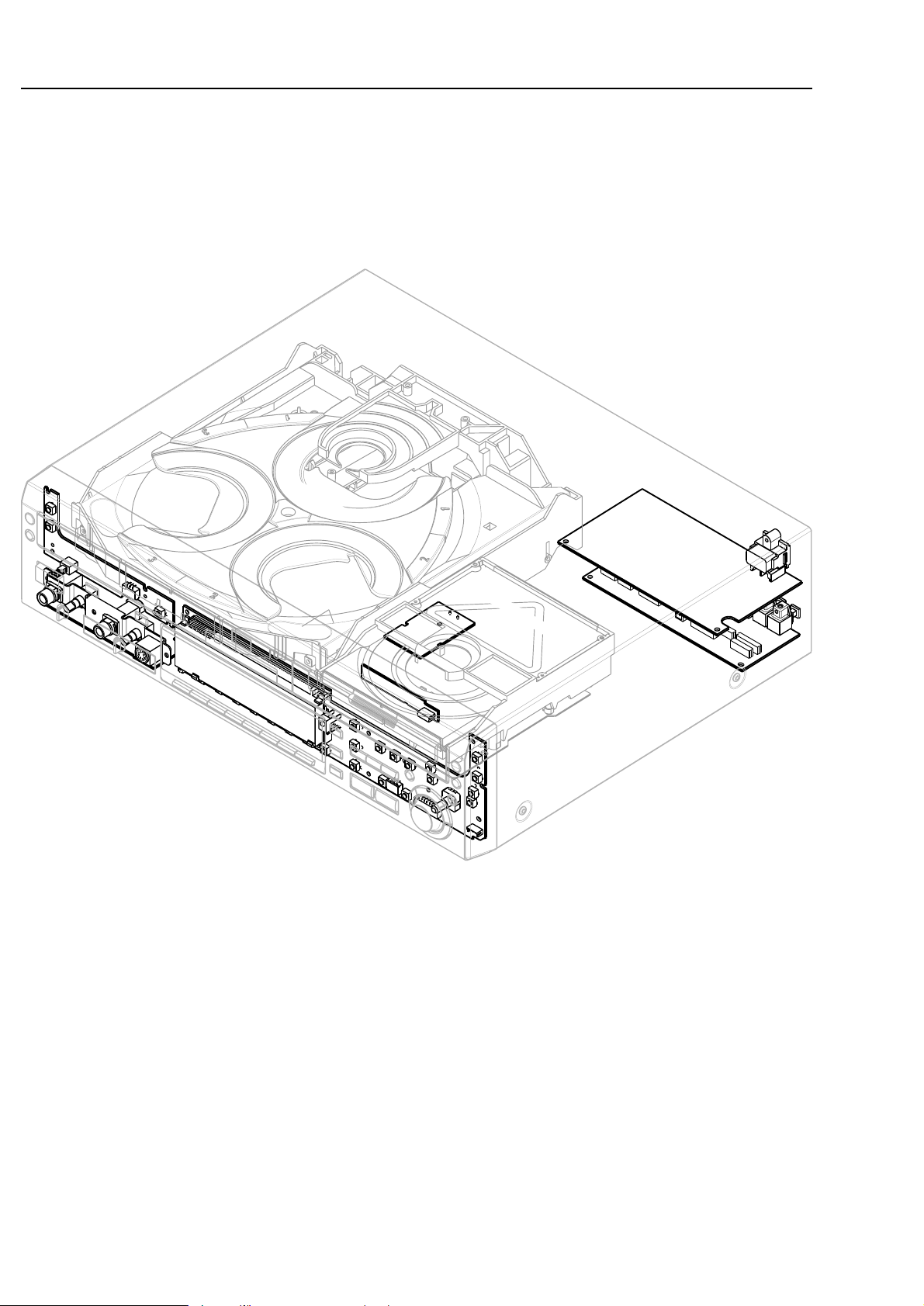
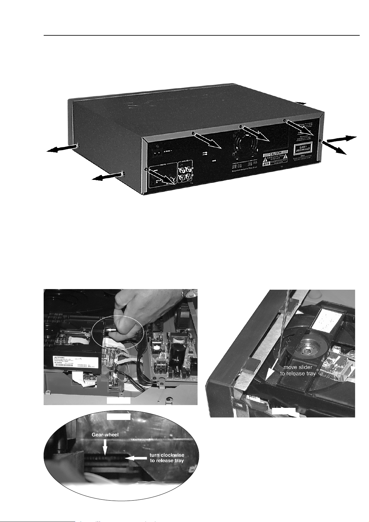
DISMANTLING INSTRUCTIONS
Dismantling the
Top Cover
picture 2
• Remove 9 screws as shown in picture 2.
• Raise top cover at the rear and pull it backwards.
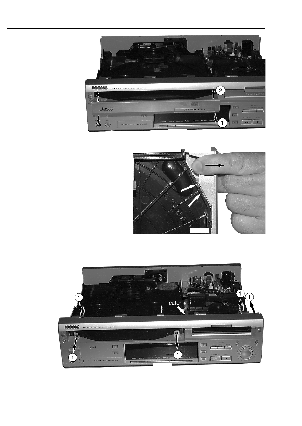
Dismantling the
Tray Covers
To dismantle the ornamental cover, the tray has to be moved out first.
This can either be done by activating the Open/Close-key or manually.
In order to avoid unnecessary loading it is recommended to move the tray out manually a few centimetres.
To release the tray manually proceed as shown in pictures 3, 4 and 5. The tray will move out a little.
Afterwards it can be pulled out as far as convenient.
Release tray of 3 Disc Changer Release tray of CDR module
picture 4
picture 5
detail
picture 3
Page 10
4-2
DISMANTLING INSTRUCTIONS
Dismantling the
Front Cabinet
picture 8
• Remove top cover and ornamental covers from the trays first →see description on page 4-1.
• Move trays back to
closed
position.
• Loosen 5 screws as shown in pictures 8 and 9.
• Release catches on top (as shown in picture 8) and catch on frame of CDR module (see also picture 10).
• Turn front cabinet away.
• Place front cabinet as shown in picture 11.
• To release the cover from the catch on the tray, pull it
frontwards on bottom side as shown in picture 6 and 7.
• Pull the cover up.
picture 6
bottom view
Dismantling the
Tray Covers
continued
picture 7
Dismantling the ornamental cover
from the
CDR-tray
functions in the same manner.
Page 11
4-3
DISMANTLING INSTRUCTIONS
Dismantling the
Front Cabinet
continued
picture 11
picture 9 picture 10
Page 12
4-4
DISMANTLING INSTRUCTIONS
• Loosen 2 screws at the rear as shown in picture 13.
• Move the complete module backwards.
• Pull the module on rear side up and turn it out.
→ see picture 14
• Put the module to a proper service position.
→ see also chapter SERVICE HINTS.
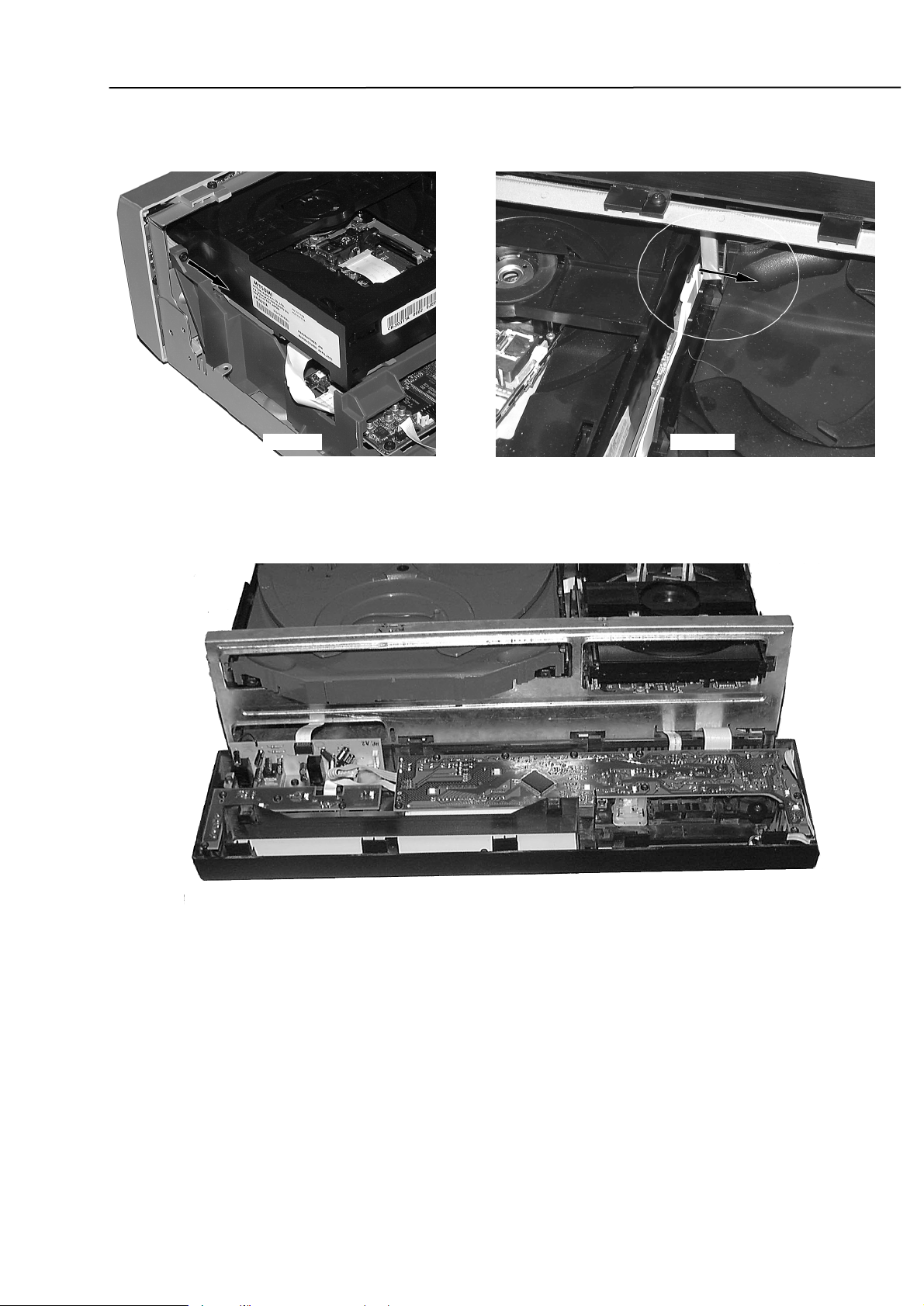
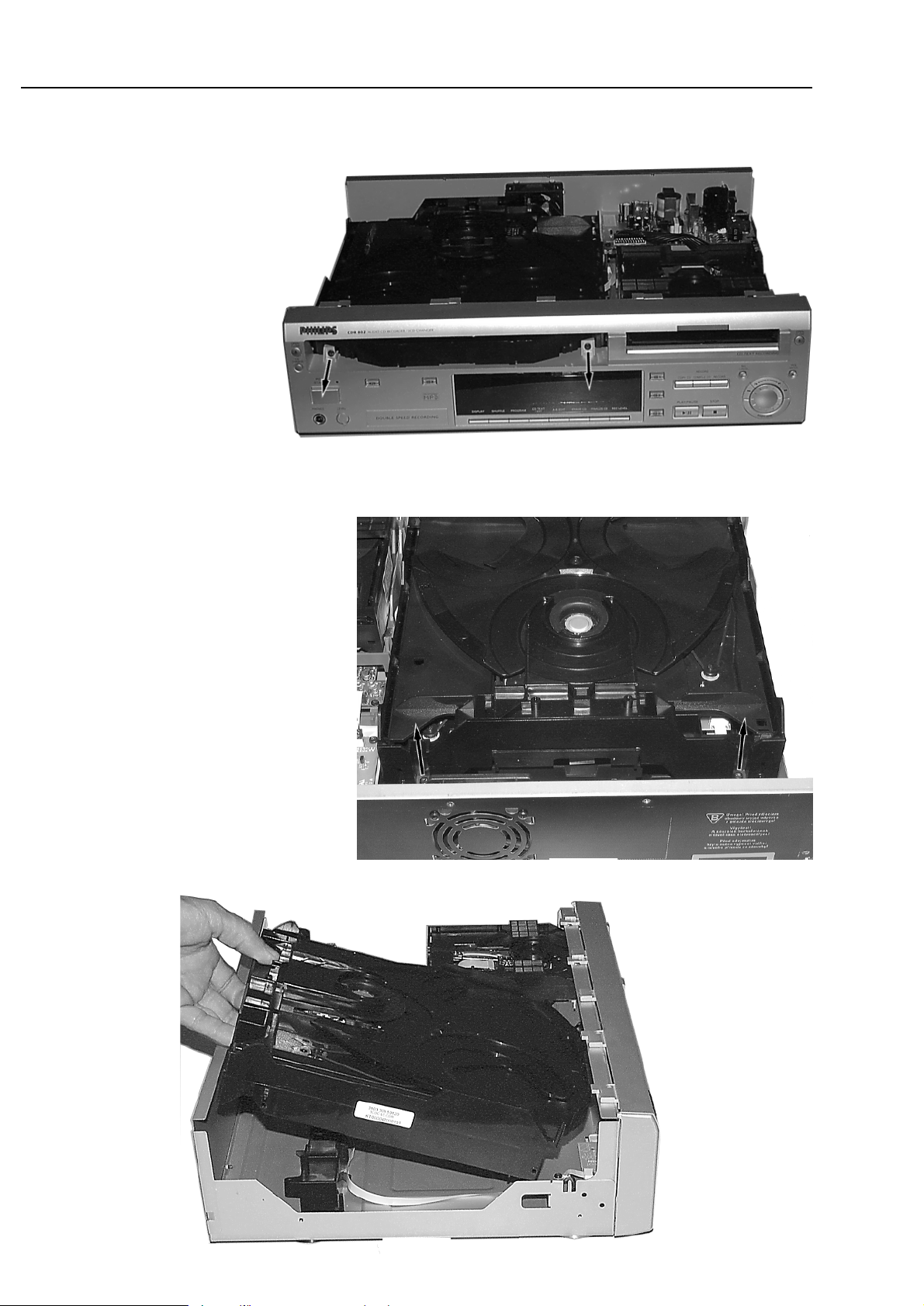
Dismantling the
3CDC module
• Remove top cover and ornamental cover from
the tray first → see description on page 4-1.
• Loosen 2 screws on front side →see picture 12.
picture 12
picture 13
picture 14
Page 13
4-5
DISMANTLING INSTRUCTIONS
Dismantling the
CDR module
• Remove top cover and ornamental cover from the tray first
→ see description on page 4-1.
• move tray back to
closed
position.
• to dismantle the complete module:
-loosen 1 screw to bottom cabinet on rear side
(see picture 16) and 1 screw to front cabinet
(see picture 17)
-disengage catch to front (see picture 15)
-move module backwards until catches to bottom cabinet
become free and pull it up.
picture 16
picture 15
Fixation by a catch on left
front-side
picture 17
Page 14
4-6
DISMANTLING INSTRUCTIONS
picture 18
Dismantling the
CDR module
continued
• Remove top cover and ornamental cover from the tray first
→ see description on page 4-1.
• to dismantle the Loader module:
-move tray completely out.
-loosen 4 screws to frame as shown in picture 18.
- put the module to a proper service position.
→ see also chapter SERVICE HINTS.
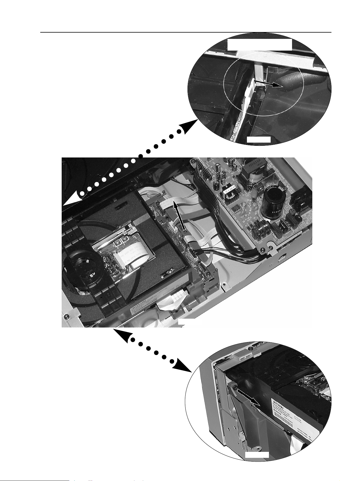
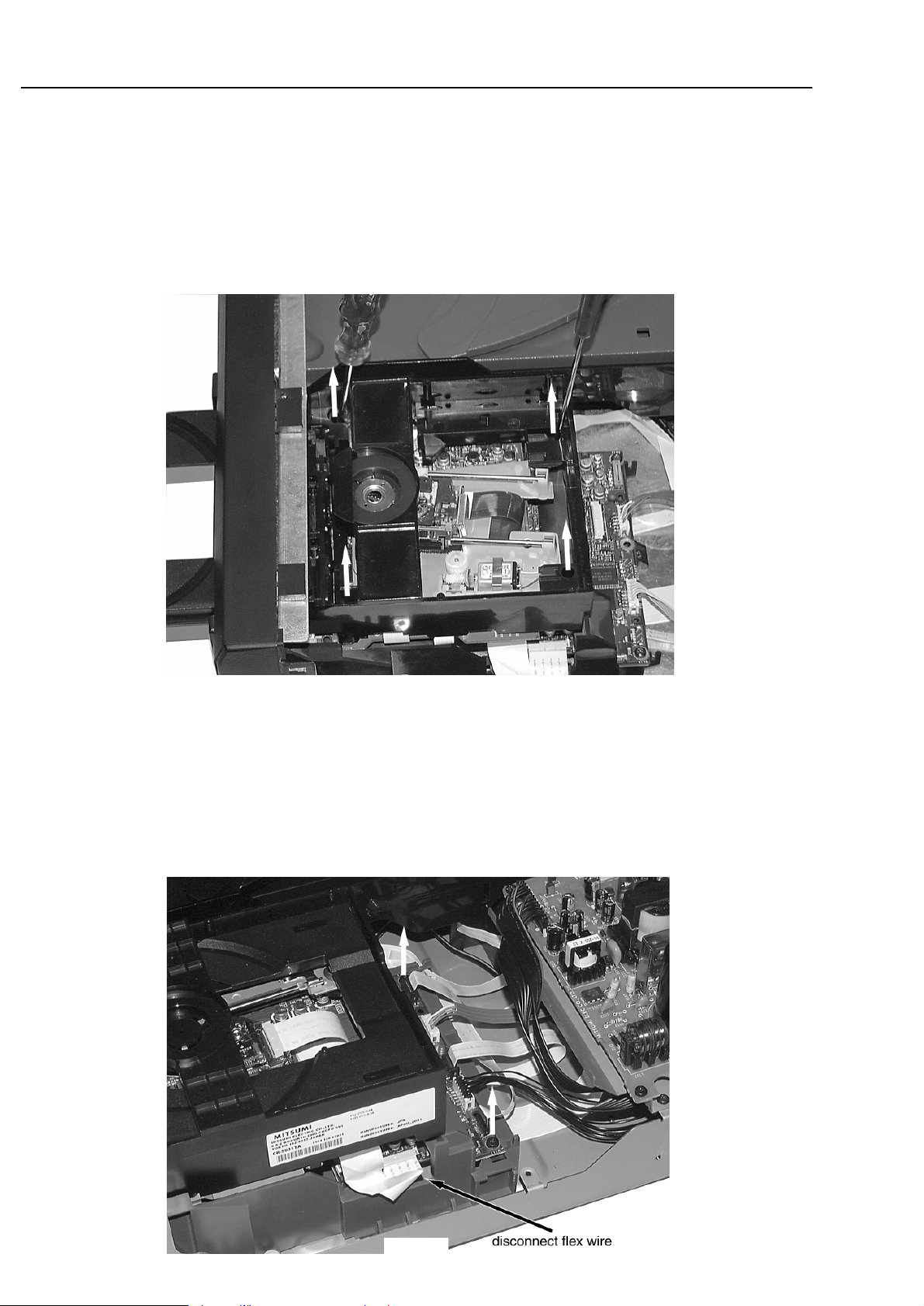
• to dismantle the MOZART Board:
-loosen 2 screws to frame as shown in picture 19.
-unlock flex foil connector and disconnect flex wire.
-pull the board out of it´s guidings (backwards).
- place the Mozart board to a proper service position.
→ see also chapter SERVICE HINTS.
picture 19
Page 15
4-7
DISMANTLING INSTRUCTIONS
Dismantling the
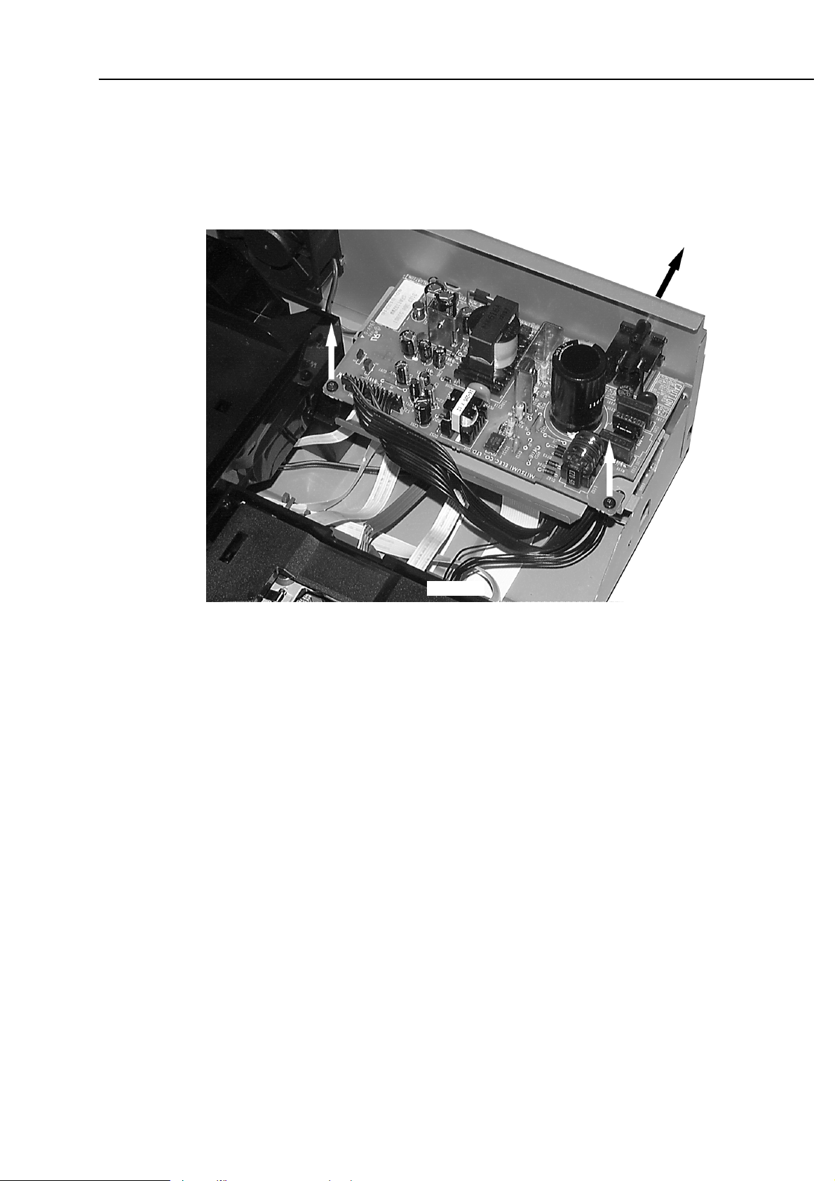
Power board
• Remove top cover first →see description on page 4-1.
• Loosen 3 screws as indicated in picture 20.
• Move the board backwards to release the mains socket.
• Lift it on the rear and turn it out.
picture 20
Page 16
4-8
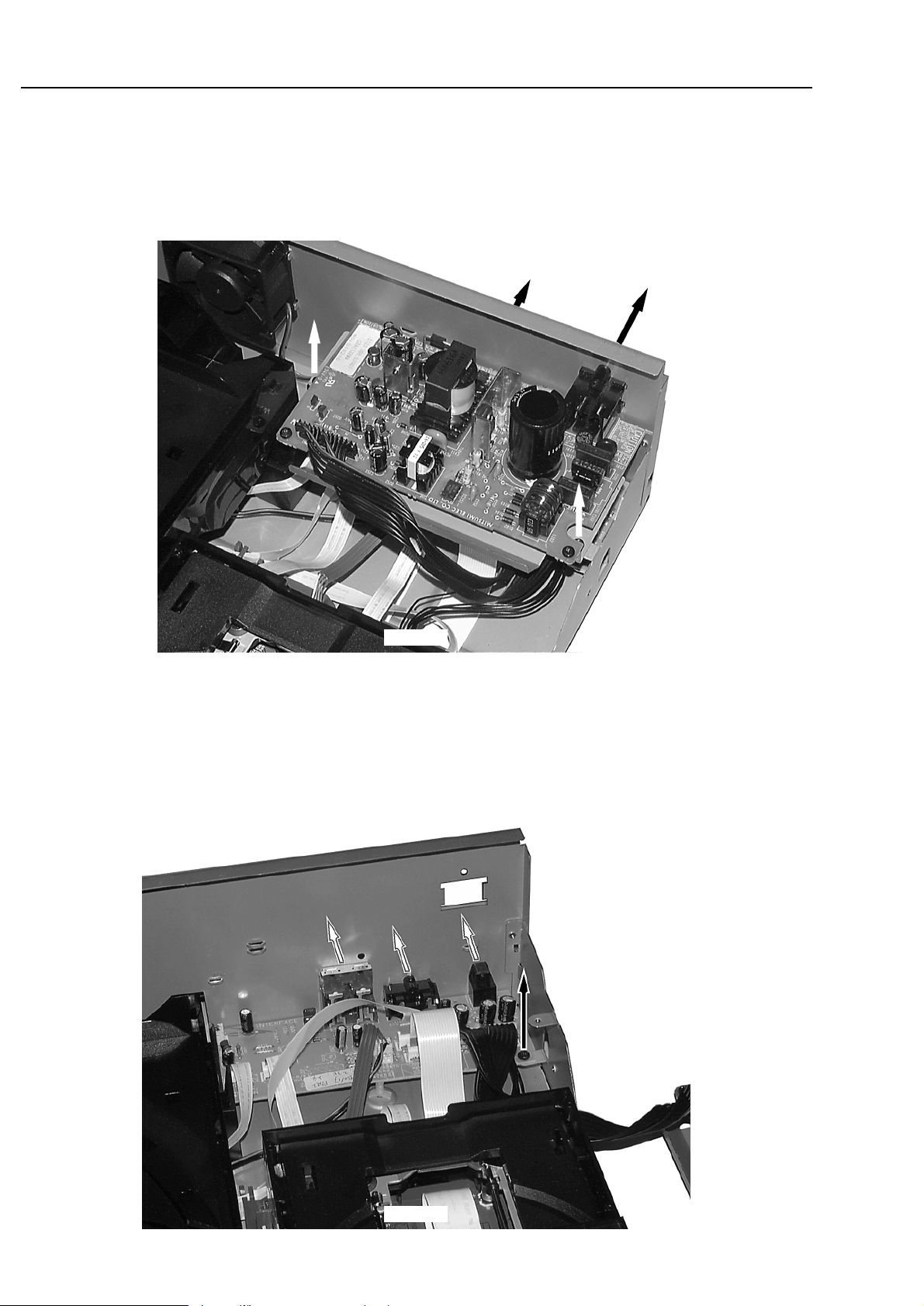
Dismantling the
Interface Board
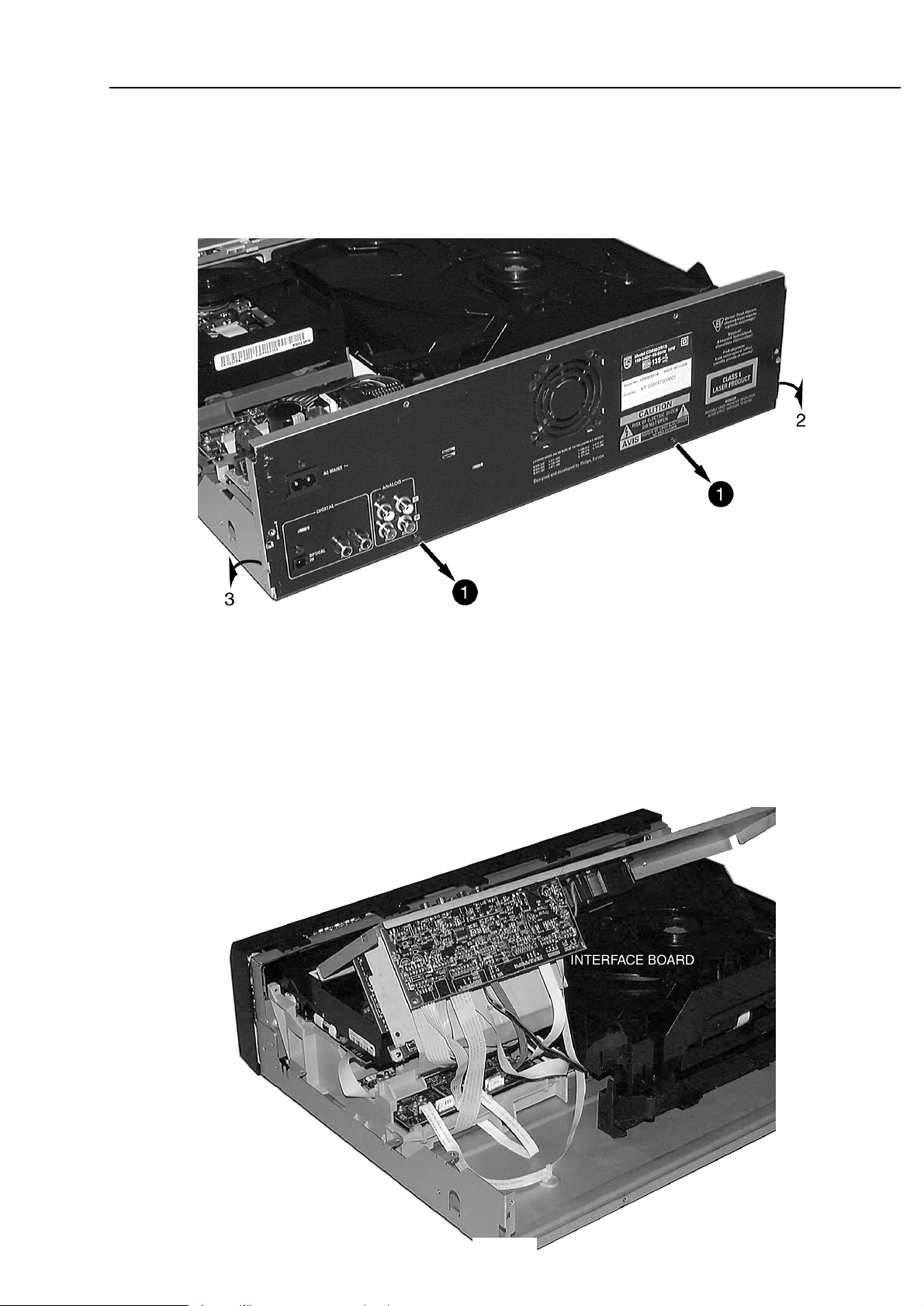
• Remove top cover first →see description on page 4-1.
• Remove Power board inclusive metal screening plate.
- Loosen 4 screws as indicated in picture 21.
- Move the combination backwards to release the mains socket.
- Lift it on the rear and turn it out.
picture 21
DISMANTLING INSTRUCTIONS
• Loosen 1 screw from the board and 3 (4) screws from sockets at
the rear plate.
• Move the Interface board backwards to release the sockets.
• place the Interface board to a proper service position.
→ see also chapter SERVICE HINTS.
picture 22
Page 17
4-9
DISMANTLING INSTRUCTIONS
picture 23
Dismantling the
Interface Board
alternative
• Remove top cover first →see description on page 4-1.
• Loosen 2 screws as shown in picture 23.
• Disengage catches to bottom bottom cabinet.
• Move rear plate backwards and turn it to a proper service position
→ see picture 24.
picture 24
Page 18
5-1
SERVICE HINTS
SERVICE TOOLS
TORX T10 screwdriver with shaftlength 150mm ......................................4822 395 50423
TORX screwdriver set SBC 163 ..............................................................4822 295 50145
Audio signal disc SBC 429......................................................................4822 397 30184
Playability test disc SBC444...................................................................4822 397 30245
Test disc 5 (disc without errors) +
Test disc 5A (disc with dropout errors, black spots and fingerprints)
SBC 426/426A ....................................................................4822 397 30096
Burn in test disc (65 min. 1kHz signal at -30dB level without "pause") ...4822 397 30155
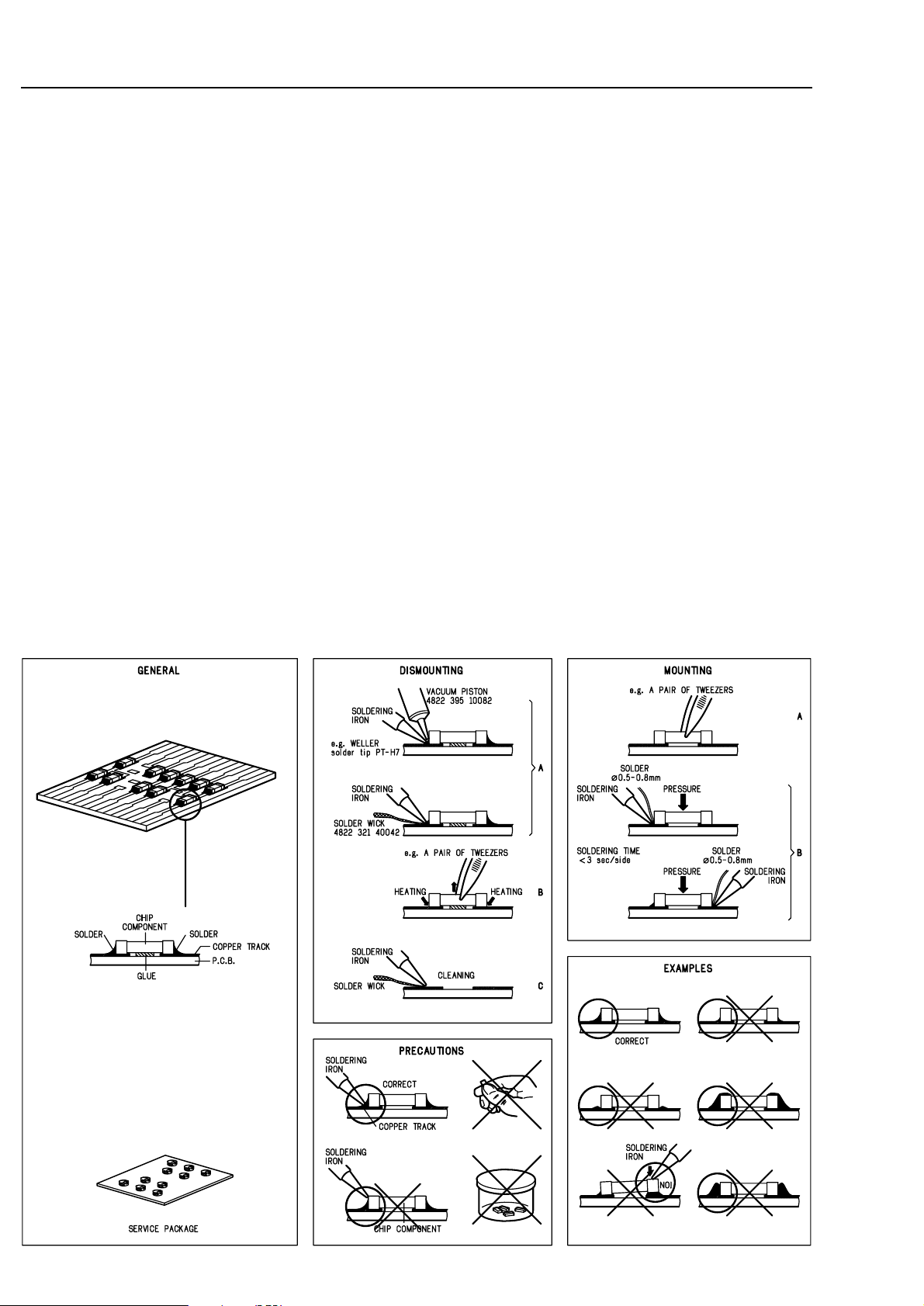
HANDLING CHIP COMPONENTS
DEALER MODE
The sets are equipped with a special DEALER MODE.
This mode blocks the trays of the CDC- and CDR module to
prevent customers from fetching out CDs from exhibition sets.
The Dealer mode can be switched on/off as follows:
1) Switch the set with the Remote Control to [Standby]
2) Press the
[DISPLAY] key at least for 5s
→ Display shows
TRAYS LOCKED else UNLOCKED
DEMO MODE
The DEMO MODE displays various features of the set and
will start automatically when no key has been pressed for
several minutes or during Standby mode.
The Demo mode can be switched on/off as follows:
1) Switch the set with the Remote Control to [Standby]
2) Press the
[STOP] key on the set at least for 5s
→ Display shows
DEMO ON else DEMO OFF
Page 19

5-2
SERVICE HINTS
General Service position
For measurements on: Power Board
For manual release of: 3CDC tray
CDR tray
Service position
Front Board
For dismantling instructions see chapter 4-1 to 4-3
picture 25
picture 26
Page 20

5-3
SERVICE HINTS
Service position
3CDC Module
picture 28
picture 27
Service position
CDR Module
picture 29
For dismantling instructions see chapter 4-5.
For dismantling instructions see chapter 4-4.
Page 21

5-4
Service position
CDR Loader
(Basic Engine)
picture 30
Service position
MOZART Board
(Back-end)
picture 31
picture 32
SERVICE HINTS
For dismantling instructions see chapter 4-6.
For dismantling instructions see chapter 4-6.
Page 22

5-5
SERVICE HINTS
Service position
Power Board
picture 33
For dismantling instructions see chapter 4-7.
Service position
Interface Board
picture 34
For dismantling instructions see chapter 4-8.
picture 35
For dismantling instructions see chapter 4-9.
Page 23

5-65-6
N
Y
KEY TEST
Display shows
1)
Numbers acc. table 2
are indicated as long as a
button is held depressed.
If a button is pressed
on the Remote Control
KEY RC is shown
and the ; flag flashes.
FFWD 6
button
pressed?
STOP
button
pressed?
N
Y
10
OPEN/CLOSE
(CDR)
FINALIZE CD
SPEED
(CDR820 only))
ERASE CD
COPY CD
CDR
AUX
CD1
20
21
22
23
24
25
99
CD2
5
KEY KEY CODE
exit test
2
3
4
5
6
7
8
9
12
15
11
RECORD
COMPILE CD
14
13
16
17
CD3
CD TEXT
/EDIT
DISPLAY
SHUFFLE
CD CHANGE
PLAY/PAUSE
OPEN/CLOSE
(CDC)
ON/OFF
18
STOP
A-B EDIT
1
0
PROGRAM
REC LEVEL
YES
/ENTER
NO
/CANCEL
6
KEY KEY CODE
KEY CODES
table 2
1)
If the ON/OFF switch is in the position
OFF
, all other keys
are blocked and display will show
99
as long any key is
held depressed.
SERVICE TESTPROGRAM
VARIOUS TESTS
CDR8xx servtest various, 07.09.01
N
Y
FORMAT EEPROM
Display shows
for 2s.
EEPROM is cleared and
default values are stored.
CD TEXT
button
pressed?
This test should only be used to clear
the EEPROM in case of a µP-"hangup".
Attention: all data are set to default values,
BLACK BOX data are not cleared.
KEY --
DISPLAY
button
pressed?
STOP
button
pressed?
N
N
Y
Y
Display shows all
segments and flags (dimmed)
for checking open circuits.
see figure 1
All LEDs are switched on.
DISPLAY TEST
fig. 1
N
Y
QUARTZ TEST
Display shows
1220±37Hz can be measur.
on (pin 27 of µP).
STOP
button
pressed?
N
Y
REW 5
button
pressed?
Tact frequency µP
(divided 10MHz)
1
10M
NEW
VXX
S
*
To leave Service Testprogram plug mains cord off.
*
In the main menu the sound settings (volume, ...),
trays and carousel work as in normal mode.
Display shows
version number
of the µP - software.
stands for Service mode
stands for Version number
of the software used in the
Front (Display) µP.
To enter Service
Testprogram hold
PLAY & CD3
buttons
depressed while
plugging mainscord in.
On/Off switch in pos.
ON
S-CDR80-VXX
Insert CD-DA disc
before starting the test
NY
Plug mains cord off
to exit
END-USER DIAGNOSTICS
Display shows:
FAILED
Display shows:
PASSED
END-USER DIAGNOSTICS
(CDR module)
To enter
END-USER DIAGNOSTICS
hold
PLAY & REC LEVEL
buttons depressed while
plugging mainscord in.
On/Off switch in pos.
ON
TEST O.K.?
Display shows for 3s each:
• Software version of
MOZART (flash ROM 7101)
• Software version of
basic engine processor
(flash EPROM 7017)
SDRAM TEST 7100
Display shows:
DTST1
CHECKSUM TEST 7101
Display shows:
DTST2
ERASE TEST 7101
Display shows:
DTST3
COMMUNICATION TEST
(UART-BUS)
Display shows:
DTST4
Flash Proms are set
to default settings.
Test planned for future software versions
- not implemented in all sets
PASS
N
Y
EEPROM TEST
Display shows
ERR
Display shows
Testpattern is written to
address 1
and
read back again
PROGRAM
button
pressed?
STOP
button
pressed?
Test ok?
N
Y
N
Y
NTC XX
N
Y
TEMPERATURE
(NTC) TEST
Display shows
XX = value in °C
AUX
button
pressed?
STOP
button
pressed?
N
Y
CDR80x
CDR82x
SERVICE TESTPROGRAM
VARIOUS TEST
Page 24

5-7 5-7
OPEN/CLOSE
button
pressed?
Y
NEXT
6
button
pressed?
N
Y
PREV
5
button
pressed?
N
Y
PLAY
button
pressed?
N
Y
CDR
MECHANICAL TEST
CDR
DC-ERASE MODE
SLIDE TESTFOCUS TEST TRAY TEST TURNTABLE
TEST
Display shows:
SLIDE
for visual inspection only
OPEN/CLOSE
button
pressed?
N
Y
N
Y
N
Slide moves
continuously in/out.
Display shows:
OPEN
(even when tray is blocked)
Tray opens.
Display shows:
CLOSE
(even when tray is blocked)
Tray closes.
Dependent on the
moving direction,
slide moves to inner
or outer end position.
N
Y
STOP
button
pressed?
Exit Mech. Testprogram
SERVICE TESTPROGRAM
CDR MODULE
Objective moves
continuously up/down.
Display shows:
FOCUS
PREV
5
button
pressed?
N
Y
YES
button
pressed?
N
Y
Turntable motor
is switched on.
Display shows:
DISC
PREV
5
button
pressed?
CD-RW disc
inserted?
N
Y
DC-ERASE
finished?
N
Y
BURN IN MODE
CDR MODULE
Display shows:
HH BI RE FE
DC-ERASE MODE
starts.
Record complete disc
from analog source
with normal speed.
Display shows:
HH BI RE FE
Complete disc
recorded?
N
Y
Error detected?
N
Y
Finalize disc
with double speed.
Display shows:
HH BI RE FE
HH stands for the number of hours
the test was running
BI stands for Burn In test
RE number of errors detected during
DC erase and write mode
FE number of errors detected during
Finalizing the disc
Turntable motor
is switched off.
Focus servo
is switched off.
CDR8xx servtest CDR module, 030901
STOP button
pressed?
Y
N
Display shows:
WRONG DISC
or
NO DISC
TESTS PLANNED FOR FUTURE SOFTWARE VERSIONS
- NOT IMPLEMENTED IN ALL SETS
N
Y
STOP button
pressed?
Y
N
Display shows:
WRONG DISC
or
NO DISC
Disc erased?
N
Y
N
Y
Complete disc will be
erased with double speed.
(starting from PMA-area
up to and including
ATIP leadout area)
The display shows the
countdown of the
remaining time required
to complete the operation:
ER mm ss
Display shows:
PASSED
mm: remaining minutes
ss: remaining seconds
STOP
button
pressed?
Exit DC-ERASE Mode
Note: With the DC-Erase mode the CD-RW can be
changed back in its original state, like a new disc.
Stopping the erase-function by switching power off
will leave the disc in an unpredictable status!
CD-RW disc
inserted?
TEST O.K.?
NN
Y
Y
N
Y
Y
CDR
ELECTRICAL TEST
Insert CD-DA disc
before starting the test
MODULE INFORMATION
MOZART BOARD DIAGNOSTIC
CDR - LOADER TEST
SDRAM TEST 7100
Display shows:
DTST1
CHECKSUM TEST 7101
Display shows:
DTST2
ERASE TEST 7101
Display shows:
DTST3
COMMUNICATION TEST
(UART-BUS)
Display shows:
DTST4
Display shows:
DERR
n
n=number of failed test
Display shows next error
FFWD
6 button
pressed?
N
Y
FFWD
6 button
pressed?
Y
FFWD
6 button
pressed?
Y
FFWD
6 button
pressed?
all errors shown?
N
N
N
TEST O.K.?
NN
Y
Y
Display shows:
BERR 1
Display shows:
PASSED
for 3s
FFWD
6 button
pressed?
CD-DA disc
inserted?
Display shows actual
playing time.
The test is performed by
playing 5s at beginning,
5s in the middle and 5s at
the end of the disc.
N
Y
Display shows:
NO DISC
FFWD
6 button
pressed?
Note: The BURN-IN mode is an endless cycle of
*
DC erase, to erase the CD-RW disc with max. laser power
*
Recording a CD-RW disc with speed N=1
*
and Finalizing with double speed
This test is intended to check the quality of a CDR loader and
to detect intermittent failures.
Exit CDR electrical Test Exit CDR electrical Test
Display shows for 5s:
MO XXXX BXXXX
• MO xxxx stands for
Software version of
MOZART
(flash ROM 7101)
• Bxxxx stands for
Software version of
Basic engine processor
(flash EPROM 7017)
With the
DISPLAY
button the info on the display can be toggled
to indicate either the status of burn in test or the temperature
measured via the NTC.
1)
1)
1)
1)
S
*
To leave Service Testprogram plug mains cord off.
*
In the main menu the sound settings (volume, ...),
trays and carousel work as in normal mode.
Display shows
version number
of the µP - software.
To enter Service
Testprogram hold
PLAY & CD3
buttons
depressed while
plugging mainscord in.
On/Off switch in pos.
ON
S-CDR80-VXX
CDR
button
pressed?
N
Y
N
Y
FINALIZE
button
pressed?
ERASE CD
button
pressed?
N
Y
RECORD
button
pressed?
N
Y
VXX
stands for Service mode
stands for Version number
of the software used in the
Front (Display) µP.
SERVICE TESTPROGRAM
CDR MODULE
Page 25

5-85-8
SERVICE TESTPROGRAM
CD/CDC MODULE
CDR8xx/CD servtest, 030901
OPEN/CLOSE
button
pressed?
NEXT
6
button
pressed?
N
Y
PREV
5
button
pressed?
N
Y
PLAY
button
pressed?
N
Y
CD or CDC
MECHANICAL TEST
SLIDE TESTFOCUS TEST TRAY TESTTURNTABLE
TEST
Display shows:
SLIDE
for visual inspection only
OPEN/CLOSE
button
pressed?
N
Y
Y
N
Y
N
Slide moves
continuously in/out.
Display shows:
OPEN
(even when tray is blocked)
Tray opens.
Display shows:
CLOSE
(even when tray is blocked)
Tray closes.
Dependent on the
moving direction,
slide moves to inner
or outer end position.
N
Y
STOP
button
pressed?
Exit Mech. Testprogram
Objective moves
continuously up/down.
Display shows:
FOCUS
PREV
5
button
pressed?
N
Y
YES
button
pressed?
N
Y
Turntable motor
is switched on.
Display shows:
DISC
PREV
5
button
pressed?
Focus servo
is switched off.
Turntable motor
is switched off.
TESTS PLANNED FOR
FUTURE SOFTWARE VERSIONS
- NOT IMPLEMENTED IN ALL SETS
N
Y
CD or CDC
LOADER TEST
TEST O.K.?
NN
Y
Y
Display shows:
BERR 1
Display shows:
PASSED
for 3s
Tray opens
FFWD
6 button
pressed?
CD-DA disc
inserted?
Display shows actual
playing time.
The test is performed by
playing 5s at beginning,
5s in the middle and 5s at
the end of the disc.
N
Y
Display shows:
WRONG DISC
or
NO DISC
OPEN/CLOSE
button
pressed?
N
Y
CD1
button
pressed?
Exit CD electrical Test Exit CD electrical Test
VXX
S
*
To leave Service Testprogram plug mains cord off.
*
In the main menu the sound settings (volume, ...),
trays and carousel work as in normal mode.
Display shows
version number
of the µP - software.
stands for Service mode
To enter Service
Testprogram hold
PLAY & CD3
buttons
depressed while
plugging mainscord in.
On/Off switch in pos.
ON
S-CDR80-VXX
CD2
button
pressed?
N
Y
stands for Version number
of the software used in the
Front (Display) µP.
set continues operation, message remains on the display until next error occurs
or any key is pressed.
Error number Error type
Error type:
Error description
E1000 Focus Error
Triggered when the focus is lost for more than 250ms while playing the CD.
E1006 Subcode Error
No valid subcode for 300ms during
PLAY
.
Slide-out error
Generated when the inner-switch did not open within approx. 250ms when the pick up is
moved from the inner position outside. Inner-switch or slide motor problems.
E1002
E1003
Slide-in error
Generated when the inner-switch did not close within approx. 6s when the pick up is
moved inside. Inner-switch or slide motor problems.
W
E1020 Focus Search Error
Triggered when the focus could not be found within 4s when starting up the CD.
F
W
W
E1001 Radial error
Triggered when the radial servo is not on track for a certain time during playing the CD.
W
W
W
W
W = Warning →
F = Fatal Error
→ set stops operation, message remains on the display.
CD ERROR CODES
table 1
E1005 Jump error.
Triggered when the servo processor counts too less tracks in a defined time during JUMPS.
This can be caused by a disturbed HF-signal (the tracks cannot be recognized exactly),
slide motor problems, track servo problems or scratched discs.
E1008 Disc motor error
Generated when the CD could not reach 75% of speed during startup within 1,2s.
W
E1007 PLL lock error
When no valid subcode was found within 300ms PLL is checked. If PLL is locked E1006
will be indicated else E1007 and the servo is stopped and restarted once again to recover
(as if the user would have pressed
STOP
and then
PLAY
immediately).
The
CD PLAY TEST
is intended to be used
for continuously playing a disc in order to
detect intermittent or not reproducible
failures. The error code indicates where
the failure can be found.
1)
Y
CD PLAY TEST
1)
(CD BURN IN TEST)
N
CD is in normal
PLAY
mode.
In case of failures
error codes acc. table 1
will be indicated
on the display.
MAINS CORD
plugged off?
N
Y
Exit Service Testprogram
CD3
button
pressed?
With the
DISPLAY
button the info on the
display can be toggled to indicate either
the status of
CD PLAY TEST
or
the temperature measured via the NTC.
2)
2)
SERVICE TESTPROGRAM
3CDC MODULE
Page 26

6-1 6-1
1307
0053
17
1304
51
1303
71
0052
15
7324F
74LVU04D
+IC
LINE_IN
1314B
DIG IN
7312
OPT. IN
1315B
+F -F
-30V
+5V
+5V EVER
+F-F-30V
+5V EVER
+12V
+5V +IC +3V3aV_AMP1+ -12V
0054
16
V_AMP1-+3V3d
HP_L
HP_R
ANA IN_R
ANA OUT_L
EBU IN COAX
ANA OUT_R
ANA IN_L
-12V
+12V
LM833D
V_AMP1+
V_AMP1-
1315A
1314A
DIGITAL
OUT
7324E
74LVU04D
+IC
7324A-D
5300
7320
74LVU04D
+IC
1306
12
1301
12
NTC
FAN
FAN CONTROL
INTERFACE BOARD
ANALOG
OUT
ANALOG
IN
15 1
1308
91
POWER_ON
POWER_ON
FAN
MUTE
3CDC SW Info
3CDC SH STR
3CDC SH CLK
3CDC SH DATA
3CDC SW Info
3CDC SH STR
3CDC SH CLK
3CDC SH DATA
NTC
EBU IN OPT.
EBU OUT
+5V
+12V
+5V
+5V
+12V
LEVEL SHIFT
BUFFER
CON1
CN101
12 1
8
1
(Supply) ON/OFF
+5V EVER
-F1
+F1
-30V
+5V
+12V
EBU IN CD10
+5V
AUDIO SIGNAL INTERFACE
DIGITAL IN / OUTCONTROL INTERFACE
SUPPLY INTERFACE
CD INTERFACE
RESET CD10
CD10 SDA
CD10 SCL
CD10 RAB
CD10 SILD
-12V
CD - CHANGER MODULE
for details see
separate block diagram
SWITCHED MODE
POWER SUPPLY
for details see
separate block diagram
CDR MODULE
for details see
separate block diagram
HEADPHONE-
MICROPHONE
BOARD
14021007 1203
1205
1761 15
1660
+12V
-12V
HP_L
HP_R
7660
3676
+12V
-12V
NJM4556AM
HEAD-
PHONE
I2C DATA
I2C CLK
RESET
EBU OUT
EBU EXT. IN
EBU IN OPT.
ANALOG IN (REC) L
ANALOG IN (REC) R
ANALOG OUT (PB) R
ANALOG OUT (PB) L
8
1
EBU
PORE
SDA
SICL
RAB
SILD
1802
IRQ
1805
91
SW Info
SHR STR
SHR CL
SHR DATA
+5V
NC
NC
+10V
1214
16
+5V
+5V
+12V
16
1302
61
1662
CDR80x, 200401
DISPLAY BOARD
FRONT-LED BOARD
KEY BOARD
left
7414
7409
MICROPROCESSOR
M30218MAFP
7403
5VST
RC5
KEY 1
JOG A
JOG B
KEY 2
2
KEY MATRIX
RESET
EEPROM
RESET
1416
1
3
1414
1
3
0051
-30V
+F-F
1
3
30
35 - 881689
63
VCC1
VCC2
99 VREF
100 AVCC
97AVSS
65VSS1
14VSS2
VEE
1400
10MHz
1394 959291 15
12
+5VST
I2C DATA
I2C CLK
+µP
+µP
+µP
23
98
96
21
19
20
5
8
6
LED red
LED blue
LED red
LED blue
+5V
+5V
blue
Rec/Pb indication
red
+5V
7
1
LED AUX
LED CDR
KEY0
ON/OFF
LED Stby
IR EYE
1485
1
7
LED AUX
LED CDR
KEY0
ON/OFF
LED Stby
POWER_ON
NTC
f
0
1418
+F -F
-30V +5V +5VST
FAN
MUTE
3CDC SW Info
3CDC SH STR
3CDC SH CLK
3CDC SH DATA
IRQ CDR
IRQ CDR
RESET CDR
I2C CLK
RESET CDR
I2C DATA
1417
+5VST
+µP
STDBY AUX CDR
ON/OFF
offon
KEY MATRIX
1480
15 11 6
TEXT TOTAL TRACK TIME TOTAL REM
STEP
CD
RW
CD
RW
COMPILE CD TRACK PROG
RECORD IN PROGRESS
SHUFFLE REPEAT ALL EDIT
REC TRACK TIME
123456789
10 11 12 13 14 15 16 17 18 19 20 +
ANALOG
FINALIZE ALC
DIGITAL
OPTICAL
12
12
JOG CONTROL
1457
I2C BUS
I2C BUS
BLOCK DIAGRAM
CDR80x
Page 27

6-26-2
1307
0053
17
1304
51
1303
71
0052
15
7324F
74LVU04D
+IC
LINE_IN
1314B
DIG IN
7312
OPT. IN
1315B
+F -F
-30V
+5V
+5V EVER
+F-F-30V
+5V EVER
+12V
+5V +IC +3V3aV_AMP1+ -12V
0054
16
V_AMP1-+3V3d
HP_L
HP_R
ANA IN_R
ANA OUT_L
EBU IN COAX
ANA OUT_R
ANA IN_L
-12V
+12V
LM833D
V_AMP1+
V_AMP1-
1315A
1314A
DIGITAL
OUT
7324E
74LVU04D
+IC
7324A-D
5300
7320
74LVU04D
+IC
1306
12
1301
12
NTC
FAN
FAN CONTROL
INTERFACE BOARD
ANALOG
OUT
ANALOG
IN
15 1
1308
91
POWER_ON
POWER_ON
FAN
MUTE
3CDC SW Info
3CDC SH STR
3CDC SH CLK
3CDC SH DATA
3CDC SW Info
3CDC SH STR
3CDC SH CLK
3CDC SH DATA
NTC
EBU IN OPT.
EBU OUT
+5V
+12V
+5V
+5V
+12V
LEVEL SHIFT
BUFFER
CON1
CN101
12 1
8
1
(Supply) ON/OFF
+5V EVER
-F1
+F1
-30V
+5V
+12V
EBU IN CD10
+5V
AUDIO SIGNAL INTERFACE
DIGITAL IN / OUTCONTROL INTERFACE
SUPPLY INTERFACE
CD INTERFACE
RESET CD10
CD10 SDA
CD10 SCL
CD10 RAB
CD10 SILD
-12V
CD - CHANGER MODULE
for details see
separate block diagram
SWITCHED MODE
POWER SUPPLY
for details see
separate block diagram
CDR MODULE
for details see
separate block diagram
HEADPHONE-
MICROPHONE
BOARD
14021007 1203
1205
1761 15
1660
+12V
-12V
HP_L
HP_R
7660
3676
+12V
-12V
NJM4556AM
HEAD-
PHONE
I2C DATA
I2C CLK
RESET
EBU OUT
EBU EXT. IN
EBU IN OPT.
ANALOG IN (REC) L
ANALOG IN (REC) R
ANALOG OUT (PB) R
ANALOG OUT (PB) L
8
1
EBU
PORE
SDA
SICL
RAB
SILD
1802
IRQ
1805
91
SW Info
SHR STR
SHR CL
SHR DATA
+5V
NC
NC
+10V
1214
16
+5V
+5V
+12V
DISPLAY BOARD
FRONT-LED BOARD
KEY BOARD
left
7414
7409
MICROPROCESSOR
M30218MAFP
7403
5VST
RC5
KEY 1
JOG A
JOG B
KEY 2
2
KEY MATRIX
RESET
EEPROM
RESET
1416
1
3
1414
1
3
0051
-30V
+F-F
1
3
30
35 - 881689
63
VCC1
VCC2
99 VREF
100 AVCC
97AVSS
65VSS1
14VSS2
VEE
1400
10MHz
1394 959291 15
12
+5VST
I2C DATA
I2C CLK
+µP
+µP
+µP
23
98
96
21
19
20
5
8
6
LED red
LED blue
LED red
LED blue
+5V
+5V
blue
Rec/Pb indication
red
+5V
7
1
LED AUX
LED CDR
KEY0
ON/OFF
LED Stby
IR EYE
1485
1
7
LED AUX
LED CDR
KEY0
ON/OFF
LED Stby
POWER_ON
NTC
f
0
1418
+F -F
-30V +5V +5VST
FAN
MUTE
3CDC SW Info
3CDC SH STR
3CDC SH CLK
3CDC SH DATA
IRQ CDR
IRQ CDR
RESET CDR
I2C CLK
RESET CDR
I2C DATA
1417
+5VST
+µP
STDBY AUX CDR
ON/OFF
offon
KEY MATRIX
1480
15 11 6
TEXT TOTAL TRACK TIME TOTAL REM
STEP
CD
RW
CD
RW
COMPILE CD TRACK PROG
RECORD IN PROGRESS
SHUFFLE REPEAT ALL EDIT
REC TRACK TIME
123456789
10 11 12 13 14 15 16 17 18 19 20 +
ANALOG
FINALIZE ALC
DIGITAL
OPTICAL
12
12
JOG CONTROL
1457
I2C BUS
1305
117
1215
117
MUTE
CLK_16
I2S DATA 4
I2S WLK 4
I2S CLK 4
KILL
CLK_16
I2S DATA 4
I2S WLK 4
I2S CLK 4
PWR ON RESET
DEEMP
I2S CLK1/GND
I2S DATA1/GND
EBU CD10
PROF_DIG_OUT
EBU OUT ENGINE/GND
I2S WLK1/GND
MUTE
NC
NC
NC
NC
I2S BUS
7322
UDA1360TS
MIC_L
MIC_R
MICROPHONE
ADC
1663
PC KEY-
BOARD
+5V
Kb DATA
Kb CLK
GND
1664
41
+5V
Kb DATA
Kb CLK
0055
4
1
22, 25
7313
OPT.OUT
1661
7661
+12V
-12V
LM833D
7662
+12V
-12V
LM833D
3677
MIC_L
MIC_R
MICROPHONE
1302
8 1
18
1662
PF2-KEYBOARD INTERFACE
I/O INTERFACE EXT. ADC/DAC
MUTE
CDR82x, 200401
I2C BUS
BLOCK DIAGRAM
CDR82x
Page 28

6-3 6-3
SDA
VCC
DOBM
D1-D5
D2-D4
7814
1876 1875
1877 1878
7873
TDA7073
HEF4094BT
LD ONLD ON
LD
MON
CD/RW
HF IN
V1
D1
D2
D3
D4
R1,R2
MOT1
REGISTER
SHIFT
SIGNAL PROCESSOR
CD10
SAA7324 (SAA7325)
TRAY
MOTOR
CAROUSEL
MOTOR
SL
D5
VDD
D3
D2
D0
RA
FO
DIODES
PHOTO
D3D2
D5D1
D4
INNER SWITCH
SWITCH INFO
LASER &
MONITOR
DIODE
TURNTABLE
MOTOR
DISC
CD MECHANISM
CAROUSEL
TRAY
MAINBOARD
DATA
SHR_CL
7801
+3,3V
7802
LASER CONTROL
&
HF AMPLIFIER
TZA1024
(TZA1025)
38
42
40
39
5,17,21,52,57
64
1
13
+5V
2
4
5
7
V4
61
2
ISLICE
3
63 51
10
11
6,14
2
3
STB
1
12
11
1,3
2
2
4
1,3
2
4
2
3
5
1
3
1
5
10
9
+3,3V
SCL
SILD
RESET
Blockdiagram 3CDC-LC(Herman) 2001-09-13
+5V
+4V
+3,3V
+10V
7815
+5V
6801
BLOCK DIAGRAM 3CDC-LC
+10V
15
16
5V1
V
t
EN1
CD DRIVE UP/DOWN SWITCH
1881
1880
TRAY SWITCH
1882
CD POS.1 SWITCH
POS. RECOGNITION
6
7
4
5
1882 closed if carousel is in Position 1.
1883
1883 open if carousel is in a valid Play-Position.
Closed if the tray is in one endposition.
Open during movement.
Open if the drive is in one endposition.
Closed during movement.
VDD (pin 16)
EN1 (pin 15)
Power on
FOCUS
MOTOR
RADIAL
MOTOR
SLEDGE
MOTOR
MOTOR
TURNTABLE
55
54
56
59
19
15
34
3
7803
M63000
TTM+
TTM-
SLEDGEB-
SLEDGEB+
RADB-
RADB+
FOCB-
FOCB+
5
6
3
4
2
8
7
7
RAB
1802
RESET
SDA
EBU OUT
EBU
EBU_GND
1
GND
5
3
SHR-DATA
2
SHR_CL
4
1
SHR_STR
NC
SWITCH INFO
1805
6
8
9
1805
CDR Version
Communication CD10
with CDR Module-µP
Communication
with Front-µP
Digital Audio
SICL
SILD
+5V
NC
+10V
GND
Supply
SPEEDSEL
Low = 4x speed
Low = 2x speed
High = 1x speed
High amplification
(4x speed)
Low amplification
(1x and 2x speed)
CDR Version
VAM2201, VAM2202, VAM2204
RAB
41
7805
7804
EQSELEQSEL
62
12
to/from
CDR Module
MOZART Board
1205
to/from
Interface Board
1308
BLOCK DIAGRAM
3CDC MODULE
Page 29

6-46-4
MOZART
IC
CORE
SUPPLY
I/O
SUPPLY
SUPPLY
SUPPLY
PLL
OSC
JTAG/BDM
SDRAM
2MB
1MB
FLASH
CONTROL
ADRESS
DATA
CONTROL
EBUIN2
I2S
1 IN/OUT
/2
74LV74D
MCF5248
7100
7101
7000
7004
DC/DC
7201
DAC ADC
OPAMP
circuitry
Potmeter
ANALOG
SWITCH
3
I2S2 I2S3
3
7312
7301
7401
7402
7311
7300
16
20
8
3
DC/DC
6204
GND
DC/DC
DC/DC
DC/DC
DC/DC
7202
7200
7208
7209
+5V
+12V
3V3
2V5
-12V
-8VA
-5VA
-8VA
EBU1 (PB)
Reset CD10
SDA,SICL,Rab, Sild
PWR ON RST
CLK 16
PLAYBACK
ROUTING
FREYA EAN
FREYA EAN
Mute, Attenuation, Deemphasis
RS232
CD TEXT
I2S1(in/out)
EBU2 (Pb)
1201
1205
1214
C
D
C
M
O
D
U
L
E
OPAMP
circuitry
7401
7400
7400
1203
1215
13051304
1402
1303
+5VA
+8VA
"MOZART" BOARD CDR2001
EBU Dig_Opt Out
EBU4 Ext INI
Pro Dig Out
EBU3 opt IN
EBU3 COAX
BUFFER
ADC CLKDAC CLK
ZERO
A_Left_In
A_Right_In
A_Out_Left
A_Out_Right
+8VA-8VA
INTERFACE BOARD
D
I
S
P
L
A
Y
B
O
A
R
D
I2C
IRQ FRONT
VCXO
FILTER
Xtrim
CLK 33,86MHz
2V5
GND 3V3
3V3 3V3
GND
GND GND
1007 1417
1 23
4
5
5
6
FLEX
36p
FLEX
8p
FLEX
17p
FLEX
7p
+5V
IO CLK 16
I2S
1
KILL
I2S
4
PWR ON RST
MUTE, ATT,
DEEMP.
EBU EXT INI
EBU EXT INI
EBU DIG
OPT OUT
PRO DIG OUT
EBU IN FREYA
PWR ON RST
I2C
IRQ FRONT
2
4
4
3
4
3
FREYA CLK
2
7010
Kill
KILL
circuitry
7002
1005
B
A
S
I
C
E
N
G
I
N
E
Mute,
Deem-
phasis
Kill out
FLEX
CONTROL
INTERFACE
AUDIO SIGNAL
INTERFACE
SEPARATE AD/DA
INTERFACE
DIGITAL
INTERFACE
6p
I2S4 IN
EBU DIG
OPT OUT
OPAMP
circuitry
6202
CD R/W
I2S
INTERFACE
030901
1802
COPY ANALOG
0052
BLOCK DIAGRAM
CDR MODULE
Page 30

6-5 6-5
D207
Q202
BLOCK DIAGRAM
SWITCHED MODE POWER SUPPLY /
European & USA version (/00 & /17)
CN101
MAINS SOCKET
F101
T2A
Lightning
Protection
L101, L102
EMI-filter
T102
6,8V
22V
+5V EVER
overvoltage
protection
Q151
PC151
PC102
switch on/off
regulation
regulation
IC251
D251
D252
Q152
R152
C105
C251
D201
D206
C206
CON1
1
12
ON/OFF
+5V EVER
+F1
-F1
-30V
+5V
+12V
-12V
Q251
Q202
22V
T101
27V
+12V
overvoltage
protection
C208
D203
C204
-12V
C202
D202
C201
+5V
+5V
IC201
Q101
Q104
on/off
switching
transistor
reference
PC101
Q103
R222
R209
D204
D208
C205
-30V
+F
-F
switching
transistor
reference
Blockdiagram SMPS CDR8xx, 040901
BLOCK DIAGRAM
SWITCHED MODE POWER SUPPLY /
WorldWide version (/01)
Blockdiagram SMPS CDR8xxWW, 040901
T102
6,8V
+5V EVER
overvoltage
protection
PC151
PC102
switch on/off
regulation
regulation
IC251
D251
D252
R152
C105
C251
Q251
22V
27V
T101
+5V
IC201
Q101
reference
PC101
switching
transistor
sense
reference
54
8
7
1
2
3
S
3
4
6
2
I
sense
out
on/off
Vcc
GND
feedback
5
8
7
1
R
Q
Vcc
BUFFER
OVERVOLTAGE
PROTECTION
OSCILLATOR
BIAS
PWM
+
-
-
IC101
PWM CONTROLLER
CN101
MAINS SOCKET
F101
T2A
Lightning
Protection
L101, L102
EMI-filter
IC151
PWM CONTROLLER
CON1
1
12
ON/OFF
+5V EVER
+F1
-F1
-30V
+5V
+12V
-12V
D201
D206
C206
Q202
27V
+12V
overvoltage
protection
C208
D203
C204
-12V
C202
D202
C201
+5V
R209
D204
D208
C205
-30V
+F
-F
BLOCK DIAGRAM
POWER SUPPLY
Page 31

6-66-6
LED_blue
FFC SIDE ENTRY
EH TOP ENTRY
EH SIDE ENTRY
DIPMATE
BOARD to BOARD JQ
FFC TOP ENTRY
LEGEND
PH TOP ENTRY
PH SIDE ENTRY
XH SIDE ENTRY
FLASH TOP ENTRY
FFC TOP ENTRY
CABLE 1 to n
1mm PITCH
1203
+F
-F
-30V
+5Vever
ON/OFF
+12V
+12V
GND
GND
+5V
+5V
-12V
112
CON1
GND
CD10 SDA
CD10 SCL
CD10 RAB
CD10 SILD
Reset CD10
EBU IN CD10
EBUGND
1802
+5V
EBUOUT
EBUINOpt./GNDD
EBUINCoax
GNDD
1
ANA OUT LEFT
GND A
ANA OUT RIGHT
GND A
ANA IN RIGHT
GND A
ANA IN LEFT
175668
1402
+5V
+5V
GNDD
GNDD
GNDS
+12V
1
1214
GNDD/Shield
I2C-Data
GNDD
I2CClock
Reset
IRQREQ
11
1007
GND
SDA
SICL
RAB
SILD
(RESET)PORE
EBU
EBUGND
8
1
1205
NC
SHR_DATA
SHR_CL
SHR_STR
SW_INFO
+10V
GND
+5V
NC
19
1805
1416
Key_ON/OFF
LED_Stby
LED_AUX
LED_CDR
Key0
GND_Key
GND
1
7
GND
I2C_Data
GND
I2C_CLK
Reset
IRQ CDR
16
1417
3CDC_SH_Data
3CDC_Sh_CLK
3CDC_Sh_Str
3CDC_SW_Info
Mute
Fan
Power_ON
GND
GND
+5V_ever
+5V
NTC
-30V
-F
+F
115
13
13
1418
LED_red
+5V
1414
LED_red
+5V
LED_blue
0051
HP RIGHT
+12V
HP LEFT
-12V
GND
MIC RIGHT/GND
GNDMIC
MIC LEFT
1662
ON/OFF
LED_Stdby
LED_AUX
LED_CDR
Key0
GND_Key
GND
17
1485
8006(195mm)
OP-HR/3p
8007(220mm)
OP-HR/12p
8004(160mm)
OP-PH/6p
CD R/W MODULE 2001
MOZART BOARD
componentside view
KEY BOARD left
copperside view
HEADPHONE
BOARD
componentside view
SWITCHED MODE
POWER SUPPLY
componentside view
16
18
FRONT LED BOARD
copperside view
CD-CHANGER MODULE
3CDC-LC (CDR 2x)
MAIN BOARD
componentside view
13141315
NTC
HP RIGHT
+12V
HP LEFT
-12V
GND
MICRIGHT/GND
GNDMIC
MICLEFT
NC
SHR_DATA
SHR_CL
SHR_STR
SW_INFO
+10V
GND
+5V
NC
1308
+5V
EBUOUT
EBUINOpt./GNDD
EBUINCoax
GNDD
15
18 7 1
1306
ANA
OUT LEFT
GND A
ANA OUT
RIGHT
GNDAANA INRIGHT
GND A
ANA
INLEFT
1
19
1303
+5V
+5V
GNDD
GNDD
GNDS
+12V
16
0054
3CDC_SH_Data
3CDC_Sh_CLK
3CDC_Sh_Str
3CDC_SW_info
Mute
Fan
Power_ON
GND
GND
+5V_ever
+5V
NTC
-30V-F+F
115
1307
+F
-F
-30V
+5Vever
ON/OFF
+12V
+12V
GND
GND
+5V
+5V
-12V
1715
0053
0052
1
1301
7313 7312
Optical
IN
Optical
OUT
Digital
IN/OUT
Line
IN/OUT
8009(220mm)
OP-HR/2p
1304
FAN
1302
INTERFACE BOARD
componentside view
DISPLAY BOARD
copperside view
8005(80mm)
FFC1,25/7p/ AD
to chassis
8011
8011 for layout stage .5 only
will be replaced by a contact spring
from layout stage .6 onwards
(100mm)
8016(340mm)
FFC1,25/15p/ AD
8008(340mm)
FFC1,25/6p/BD
8001(140mm)
PH/5p
8003(160mm)
FFC1,25/7p/BD
(8007, part of Changer Module)
FFC1,0/ 8p/ AD
8014(340mm)
FFC1,25/9p/ AD
wiring diagram CDR80x/82x, 300801
(340mm)
8012(480mm)
onlyCDR80x
FFC1,25/6p/ BD
KILL
CLK_16
GNDD
IIS_DATA4
MUTE
IIS_WLK4
GNDD
IIS_CLK4
PWR_ON_RESET
IIS_WLK1/GNDD
DEEMP
IIS_CLK1/GNDD
IIS_DATA1/GNDD
GNDD
EBU_CD10
PROF_DIG_OUT
EBU_OUT_ENGINE/GNDD
117
1215
8002(140mm)
only CDR82x
17 1
KILL
CLK_16
GNDD
IIS_DATA4
MUTE
IIS_WLK4
GNDD
IIS_CLK4
PWR_ON_RESET
IIS_WLK1/GNDD
DEEMP
IIS_CLK1/GNDD
IIS_DA
TA1/GNDD
GNDD
EBU_CD10
PROF_DIG_OUT
EBU_OUT_ENGINE/GNDD
1305
FFC1,0/17p/ AD
8013(480mm)
onlyCDR82x
FFC1,25/8p/ BD
Kb_+5V
Kb_Data
Kb_CLK
GND
1
4
0055
Kb_+5V
Kb_Data
Kb_CLK
GND
1664
8017(100mm)
OP-HR/4p
only CDR82x
14
WIRING DIAGRAM
For service code numbers of flexfoil cables see mechanical partslist.
Page 32

-30,7V -29,2V
-29,9V
4,8±0,45V
floating
4,5/0V
5±0,25V
5±0,25V
12
+0,6
/
-1,2
V
-11,5
+1,5
/
-1,1
V
-29,3±2,2V
typ.-25V
typ.-20V
300V
300V
5V
5V
5V
4V
5V
4V
12V
-12V
-32V
-20V
-25V
2,5V
2,5V
1,2V
0V
4,5V
300V
1,9V
1,9V
0,1V
16,5V
-0,3V
0,2V
0,2V
1,1V
1,1V
6V
1,1V
. . . V DC VOLTAGES MEASURED IN
STOP MODE
UNLESS STATED OTHERWISE
MAINS VOLTAGE 230V (120V
USA
)
PRIMARY MEASURED AGAINST
JUNCTION D103/D104
EVM
V
Switched Mode Power Supply / EU + USA version (/00/17)
to Interface Board
0052/0053
.......
USA
for USA version only
LEGEND
Switched Mode Power Supply, EU+USA versions, 300701
(SRA1134EK+SRA1133UC combined)
EU version USA version
22
USA
470k
USA
470k
USA
2200pF
USA
10
USA
1000pF
USA
220/200
USA
33n/400
USA
100p/1k
USA
0,01/50
USA
2200p/50
USA
220/1
USA
180k
USA
27k
USA
18k
USA
180k
USA
30V
27V
22V
6,8V
3V
22V
7-1 7-1
for orientation only
POWER BOARD / copper side view
USA and European version
SMPS CDR8xx,EU+USA, 300701
SRA1134EK+SRA1133UC
R111
R202
R203
R210
R204
C110
C113
R153
R156
R256
R257
R252
R212
R213
R254R253
C207
C152
C153
C109
POWER BOARD / component side view
USA and European version
L102
L101
R101
C102
C101
CN101
Z101
F101
R114
R104
R106
Q103
Q101
D110
R102
R151
R155
Q152
Q151
R152
D151
D153
R103
D109
D203
R222(R221
USA
)
R201
IC201
D108
R117
R112
R115
D111
R120
C108
Q104
R108
C105
D101
D103
D104
D102
R158
T101
T102
R119
C11
R154
C111
PC151
PC101
PC102
D201
C201
C202
C203
L201
L202
D202
C208
C210
C205
C253
C211
C254
C251
IC251
L204
Q202
Q251
L251
R251
D207
R220
R255
CON 1
C206
L203
D208
D251
D252
D204
C204
D206
R205
R209
SMPS CDR8xx,EU+USA, 300701
SRA1134EK+SRA1133UC
Page 33

. . . V DC VOLTAGES MEASURED IN
STOP MODE
UNLESS STATED OTHERWISE.
MAINS VOLTAGE 230V/120V.
PRIMARY MEASURED AGAINST
JUNCTION D103/D104.
EVM
V
-30,7V -29,2V
-29,9V
4,8±0,45V
floating
4,5/0V
5±0,25V
5±0,25V
12
+0,6
/
-1,2
V
-11,5
+1,5
/
-1,1
V
-29,3±2,2V
typ.-25V
typ.-20V
5V
5V
4V
12V
-12V
-32V
-20V
-25V
2,5V
5V
5V
4V
2,5V
0V
4,5V
0,1V
16V
0V
1,2/2,1V
1/2,4V
300/160V
300/160V0,8V
5,9V
300/160V
3,4V
1,1/1,4V
1/1,2V
1,3V/2,7V
Switched Mode Power Supply / World Wide version (/01)
Switched Mode Power Supply, WW version, 300701
(SRA1132WW)
.......
USA
for USA version only
LEGEND
to Interface Board
0052/0053
IC101
45
Vcc
Out
Osc
GND
Feed
back
Osc on/off
I
sense
18
45
18
30V
27V
6,8V
22V
27V
7-27-2
POWER BOARD / copper side view
World Wide version
SMPS CDR8xx,WW, 310701
SRA1132WW
R202
C215
R203
R210
C216
R204
C114
R115
R113
R118
C113
C106
R119
R120
R256
R257
R252
R212
R213
R254R253
C207
R255
C151
C109
POWER BOARD / component side view
World Wide version
SMPS CDR8xx,WW, 310701
SRA1132WW
L102
L101
R101
C102
C101
CN101
Z101
F101
R152
C105
D101
D103
D104
D102
Q101
D111
R151
R114
R116
IC101
R117
D110
R107
D108
IC151
D112
R131
R132
R133
D107
C110
R105
C152
C112
T101
T102
C111
PC151
C211
C254
C253
C251
IC251
L204
L251
R251
D251
D252
C205
Q202
Q251
D207
R220
CON 1
L203
L202
D202
D208
C208
C210
C206
D204
R209
D203
L205
R201
IC201
PC101
PC102
D201
C201
C202
C203
L201
C204
D206
R205
R217
for orientation only
Page 34

7-3 7-3
GRID BUFFERS
1664
14850051
1007 1307
F454 I15
F455 G15
F456 G15
F457 G15
F458 G15
F459 G15
F460 G15
F461 H15
F462 E15
F463 E15
F464 E15
F465 E15
F466 E15
F421 C15
F422 C15
F423 C15
F424 C15
F425 D15
F426 G12
F427 G13
F428 H11
F429 H12
F430 H11
F431 H12
F433 I12
F434 I11
F435 I12
F436 I11
F437 I12
F438 J11
F439 J12
F440 J11
F441 J12
F442 K11
F443 K12
F444 K11
F445 K12
F446 K11
F447 K12
F448 J15
F449 K15
F450 K15
F451 K15
F452 I15
F453 I15
7408 K9
7409 J1
7410 G13
7411 G15
7412 I14
7413 I15
7414 C9
7415 K15
7416 K4
7417 A1
7418 A2
F400 G2
F401 G3
F402 G2
F403 G3
F404 H3
F405 H3
F406 B11
F407 E10
F408 F10
F409 J4
F410 A4
F411 B11
F412 A15
F413 A15
F414 B15
F415 B15
F416 B15
F417 B15
F418 B15
F419 B15
F420 C15
3495 I14
3496 I14
3498 J14
3499 I8
3500 J15
3501 K14
3502 K15
3503 I10
3504 I10
3505 K5
3506 K4
3510 E12
3511 G11
3512 G12
3513 I1
3514 B1
3515 B2
3516 C13
5400 B13
5402 J15
6400 A11
6428 K7
6429 K5
6431 K6
6432 K9
6433 K10
6434 I9
7402 A10
7403 I3
7405 E12
7406 K6
7407 K8
3461 H12
3462 H12
3463 H12
3464 I12
3465 I12
3466 J12
3467 J12
3468 J12
3469 K12
3470 K12
3471 E12
3472 F13
3473 F13
3474 A4
3475 B11
3477 K6
3478 K5
3479 K8
3480 K8
3481 K10
3482 K9
3484 J2
3485 K2
3486 J2
3487 K2
3488 C15
3489 F14
3490 G14
3491 H14
3492 G15
3493 H14
3494 H15
13 14 15 16
A
B
C
D
E
F
G
H
I
J
K
A
B
C
D
E
F
G
H
I
J
K
0055 J15
1400 F11
1414 I15
1416 F15
1417 D15
33343536
12345678910111213141516
12345678
*
*
*
for CDR82x only
GND
I2C_Data
GND
CDR80x: 3514, 3515 = 0 Ohm
EEPROM
KEY LIGHTING
(CDR82x)
SPEED
CD3
CD2
CD1
YES
I2C_CLK
Reset
IRQ
ROTARY ENCODER
10MHz
IR EYE
RESET
DISPLAY BOARD
9101112
1418 A15
1419 I9
1420 G12
1421 H13
1422 H13
1423 H13
1424 I13
1425 I13
1426 J13
1427 J13
1428 K13
1429 K13
1430 K13
1431 G13
1432 H12
1433 H12
1434 H12
1435 I12
1436 I12
1437 J12
1438 J12
1439 K12
1440 K12
1441 K12
2400 I4
2401 J4
2402 J10
2403 J10
2404 G12
blue
for
CDR82x
only
2405 G13
2406 E11
2407 E10
2408 F10
2409 F11
2410 F12
2411 E13
2412 F12
2413 B4
2414 B11
2415 B13
2416 J1
2418 C13
2420 D15
2421 A2
3400 C1
3401 C1
3402 C1
3403 D1
3404 D1
3405 D1
3406 D1
3407 D1
3408 E1
3409 E1
3410 E1
3411 E1
3412 E1
3413 E1
3414 F1
3415 F1
3416 F1
3417 F1
3418 F1
3419 G1
3420 I5
3421 I5
3422 K14
3423 I6
3424 I6
3425 I6
3426 I7
3427 I8
3428 I8
3429 I8
3430 J8
3431 I5
3432 I5
3433 I6
3434 I7
3435 I8
3436 I8
3437 J9
3438 I4
3439 I4
3440 J4
3441 I10
3442 I9
3443 G10
3444 G10
3445 G10
3446 G10
3447 G10
3448 G10
3449 G11
3450 H11
3451 H11
3452 H11
3453 I11
3454 I11
3455 J11
3456 J11
3457 J11
3458 K11
3459 K11
3460 G12
7
69 68
60659 56 55 54 48 47 46 45 44 4342 41 40
98
32 31 30 29 28 27 26 25 2453 52 51 50549
7402
23 22 21 20219 18 17 16 15 1413 121110
10n
2420
1
39 38 37
180p
2421
CDR80x: 3474= 3,9 Ohm
CDR82x: 3474= 0 Ohm
**
**
for CDR82x only
CDR82x: 3514, 3515 = 120 Ohm
2R2
3516
D
1K
3420
D
100n
2406
D
3474
3R9
2414
47u
2413
47u
15p
2409
D
100n
D
D
D
2400
3440
1K
100R
3438
GP1U28XP
7403
3
GND4MT
1OUT
VSUP
2
D
3439
10K
7405
BC847B
1K
2410
10n
2412
10n
3471
2n2
220K
3473
D
2401
KEY
1400
CSTS
2411
D
D
F410
D
F406
3472
220K
F409
D
10K
3475
15p
2408
BZX79-B3V9
6400
D
2402
10n
24
MT1 MT2
5
10K
3442
10K
EC12E24404
1419
13
F412
3441
F411
560R
3454
390R
3453
270R
3452
150R
3450
220R
3451
1n
2404
+5V+5V
2403
10n
1433
1435
Finalize
1434
Rec_Level
CD3
CD2
1432
1K2
34563458
3K9 820R
3455
1K8
3457
10K
3459
1440
Shuffle
1441
Display
Text
1438
Track_Edit
1439
Prog.
1513
1436
Erase
1437
262524
23
302928
34
1663 8999
65 14
10
11
79
2221201918
17
12
33
735
4
8
6
27
46454443424140393837
83
3635
82 81
80
60
59
58
578556
55
5453525150494847
84
77
76
75
74
73
72
71
70
698668
67
66
64
62
61
95 94 93 92 91 90 100
97 32931
1
2
88 87
78
470R
3428
M30218MAFP
7414
98 96
470R
3427
2
3
4
5
6
7
8
9
3435
470R
FFC
1418
1
10
11
12
13
14
15
470R
3425 220R
3433
from/to_Interface_Board
3424
100R
470R
820R
3426
470R
3429
3430
3436
470R
3437
470R
470R
3443
470R
3445
3444
470R
470R
3432
100R
3423
220R
3431
3434
470R
3421
2K7
F405
F407
D
100n
2407
F404
2u2
5400
470R
3448
3447
470R
68K
3402
3446
470R
68K
68K
3400
68K
3401
3403
F402
F400
F401
F408
F403
3410
68K
68K
3411
68K
3408
3409
68K
3404
68K
68K
3406
3407
68K
68K
3418
68K
3405
3419
68K
68K
3416
68K
3417
68K
3412
3414
68K
68K
68K
3415
D
3413
D
47u
2415
D
F436
F438
F434
F440
F442
KEY
F444
1431
F446
390R
KEY
CD1
3462
220R
3464 3461
150R
3463
270R
2405
1n
2K7
3449
F428
F430
F426
Compl_CD
No
1423
Rec_type
1422
1421
3468
3K9
3469 3466
820R1K8
3465
560R1K2
34673470
10K
1429
O/C_CDR
1430
>>
1427
Speed
Stop
1426
Yes
1428
Play/Pause
1425
<<
1424
F435
F437
F439
F445
F441
F447
F443
KEY
CD-CD
1420
from/to_CD_R/W_Module
1
2
3
4
5
6
KEY
from/to_Mic/Headphone_Board
DIPMATE
0055
1
2
3
4
FE-ST-VK-N
1417
to_Front_LED_Board
1414
EH-B
1
2
3
F429
3460
2K7
F431
F433
F427
F418
F420
F417
F415
5
6
7
F414
F416
from/to_Key_Left_Board
FE-ST-VK-N
1416
1
2
3
4
D
F413
F425
KEY
D
F424
D
F423
F422
F419
F421
7410
BC857B
3492
100R
BC857B
7411
100R
3490
3493
10K
10K
3491
3496
10K
D
10K
3489
BC847B
7412
10K
3495
D
2K7
3494
7407
BC847B
3480
D
BC847B
7406
10K10K
3478
D
7413
BC847B
3481
100R
4K7
3487
+5V
3486
4K7
3488
6K8
D
BC847B
7408
3485
10K
3482
3513
470R
470R
7409
M24C01
E0
1
E1
2
E2
3
SCL
6
SDA
5
VCC
8
VSS
4
WC_
7
100R
3479
D
3422
10K
3477
100R
3499
1K
D
10K
3498
2416
100n
D
D
D
6433
D
3484
470R
6432
6431
6428
1N4148
6434
F451
5402
2u2
D
100R
3501
2418
47u
3500
10K
3502
100R
F462
F456
BC847B
7415
F455
F453
470R
3504
F452
3503
F454
F449
470R
F450
F448
3506
10K
F466
F465
F461
F464
F463
F459
F460
F458
F457
10R
3511
10K
3510
KEY
6429
150R
3505
D
120R
7416
BC847B
3515
120R
3514
7418
BC847B
D
BC847B
7417
10R
3512
D
+5V+5V +5V
-F
+F
-30V
+uP
LED_CDR_blue
Key2
Jog_A
Jog_B
3CDC_Sh_Data
3CDC _SH_Data
-30V
+uP
+5VST
P17
P16
P15
G4
P14
P13
P12
P11
P10
P9
P8P7P6
P5
G3
P4P3P2
P1
G16a
G15a
G14
G13
G12
G11
G2
G1
LED_Speed
LED_CDR_red
LED_CD_1
LED_CDR
LED_AUX
LED_CD_2
LED_CD_3
G10
G9
G8
G7
P36
P35G6P34
P33
P32
P31
P30
P29
P28
P27
P26
P25
G5
P24
P23
P22
P21
P20
P19
P18
Fan
Fan
Mute
NC.
3CDC_SW_Info
3CDC_SW_Info
3CDC_Sh_Str
3CDC_Sh_Str
3CDC_Sh_CLK
3CDC_Sh_CLK
+F
+F
-F
-F
-30V
-30V
NTC
NTC
+5V
+5VST
+5V_ever
Jog_B
Jog_A
NTC
Key2
Key1
Key0
Kb_CLK_stop
Kb_Data_Rx
Key_ON_OFF
LED_Stby
I2C_Data_CDR
Reset_CDR
I2C_Clk_CDR
Kb_CLK
IRQ_CDR
Power_ON
Fan
Mute
3CDC_SW_Info
3CDC_Sh_Str
3CDC_Sh_CLK
3CDC_Sh_Data
GND
GND
Power_ON
Power_ON
P12
P11
P10P9P8P7P6P5P4P3P2P1G16
G15
G14
G13
G12
G11
G10G9G8G7G6G5G4G3G2
G1
+uP
+5V
-30V
Key1
P36
P35
P34
P33
P32
P31
P30
P29
P28
P27
P26
P25
P24
P23
P22
P21
P20
P19
P18
P17
P16
P15
P14
P13
I2C_Data_CDR
I2C_Clk_CDR
Reset_CDR
IRQ_CDR
GND
Kb_CLK
Kb_Data
Kb_+5V
LED_blue
+5V
+5V
LED_red
I2C_Data_CDR
LED_CD_3
LED_CD_2
LED_CD_1
LED_CDR_blue
LED_CDR_red
+uP
+5V
+5V
LED_CDR
LED_AUX
+uP
GND
GND-Key
Key0
Key0
LED_CDR
LED_AUX
LED_Stby
LED_Stby
Key_ON_OFF
Key_ON/OFF
+uP
G15
+uP
G15a
G16
+uP
G16a
+uP
+uP
+5VST
LED_Speed
+uP
+uP
+5V
Kb_CLK
Kb_Data_Rx
Kb_CLK_stop
+uP
I2C_Clk_CDR
PORT 5
P50
P51
P52
P53
P54
P55
P56
P57
P101
P102
P103
P104
P105
P106
P107
P94
PORT P4 PORT P3 PORT P2
PORT P1
P95
P96
P97
P60
P61
P62
P63
P64
P65
P66
P67
P100
P93
P92
P91
P90
PORT P8
P87
P32
P34
P35
P36
P33
P00
P30
FTD DRIVER
RAM
P31
PORT P0
P85
P86
P47
P46
P45
P44
P43
P42
P41
P40
P02
P03
P01
PORT P6PORT P10
PORT P9
P04
P05
P06
P84
P83
P82
P81
P80
PORT 7
P77
P76
P75
P74
P73
P72
P71
P70
P27
P26
P25
P24
P23
P22
P21
P20
P37
P07
P10
P11
P12
P13
P14
P15
P16
P17
VREF
VSS1
VSS2
XCIN
XCOUT
XIN
XOUT
SIN2
SOUT2
SRDY2
SSTB2
TA0IN|TA3OUT
TA1IN|TA4OUT|TXD1
TA2IN|TA0OUT|RXD1
TA3IN|TA1OUT|CLK1
TA4I|TA2O|CTS1|RTS1|CLSK1
TB0IN
TB1IN
TB2IN
TXD0|FLD52
VCC1
VCC2
VEE
FLD5
FLD50
FLD51
FLD6
FLD7
FLD8
FLD9
INT0_
INT1_
INT2_
INT3_
INT4_
INT5_
RESET_
RXD0|FLD53
SBUSY2
SCLK21
FLD36
FLD37
FLD38
FLD39
FLD4
FLD40
FLD41
FLD42
FLD43
FLD44
FLD45
FLD46
FLD47
FLD48
FLD49
FLD21
FLD22
FLD23
FLD24
FLD25
FLD26
FLD27
FLD28
FLD29
FLD3
FLD30
FLD31
FLD32
FLD33
FLD34
FLD35
CTS0|RTS0|FLD55
DA0|CLKOUT|DIMOUT
DA1|SCLK22
FLD0
FLD1
FLD10
FLD11
FLD12
FLD13
FLD14
FLD15
FLD16
FLD17
FLD18
FLD19
FLD2
FLD20
M30218MAFP
AN0
AN1
AN2
AN3
AN4
AN5
AN6
AN7
AVCC
AVSS
CLK0|FLD54
CNVSS
ROM
CPU
CLOCK
for CDR82x only
EVM
. . . V VDC VOLTAGES MEASURED IN
STOP MODE
UNLESS STATED OTHERWISE
... /...V on/off
-30V
TB 2 ms
4,8V
+5V
4,8V
4,9V
5V
0V
5V
5V
5V
5V
5V
5V
5V
5V
5V
0V
3,3V
3,3V
5/0V
5/0V
5/0V
5/0V
5/0V
5/0V
0/5V
0/5V
0/5V
0/5V
5V
5V
5V
5V
5V
5V
5V
5V
5V
5V
5V
5V
5V
typ. 5V
typ. 5V
typ. 5V
5V
5V
0,3V
3V at 22°C
(switching threshold
typ. 2,4V on, 2,3V off)
5V
0V
0/4,9V
4,5V
3,3V
3,3V
5V
5V
5/0V
1,7/0V
0,8/0V
4,3/5V
4,3/5V
5V5V4,9V
5V 4,9V
5 ±0,25V
-29,3 ±2,2V
typ. -25V
typ. -20V
5 ±0,25V
typ. -30V
0V
5V
5V
5/0V
5/0V
3V
2,5V
4,7V
4,7V
2,3V
5V
5V
5V
5V
5V
5V
5V
5V
5V5V5V5V5V5V5V
5V
5V5V5V5V5V5V5V
5V
-28V
-28V
-28V
-28V
-28V
-28V
-28V
-28V
-28V
-28V
-28V
-28V
-28V
-28V
-28V
-28V
-30V
5V
5V
5V
5V
5V
5V
5V
5V
5V
0,7/0V 0,7/0V
0V
Communication
1,8/0V
0,7/0V 0,7/0V
pins 35-88 measured in
ServiceTestprogram - DISPLAY TEST
(all segments and flags on)
Use service testprogram: QUARTZ TEST
oscillator frequency can be measured
at this point (10 MHz. divided to 1220 Hz)
f
o
4,8 ±0,45V
floating
0,8/0V
0,2V
0,2V
5V
5V
5V
5V
0V
Front/Display CDR8xx, 120901
Page 35

7-47-4
Display Board CDR80x, 300801
2400 B8
2401 A5
2402 B14
2403 B14
2404 C8
2405 B10
2406 C7
2407 A6
2408 A7
2409 A7
2410 A7
2411 A8
2412 A7
2416 B12
2420 A11
2421 C5
3400 C4
3401 C4
3402 C4
3403 C4
3404 C4
3405 C4
3406 C4
3407 C4
3408 C3
3409 C3
3410 C3
3411 C3
3412 C3
3413 C3
3414 C3
3415 C3
3416 C3
3417 C3
3418 C2
3419 C2
3421 B3
3422 A3
3423 A6
3425 A6
3426 A8
3427 B7
3428 B7
3429 B7
3430 B7
3431 B3
3433 A6
3434 A6
3435 B7
3436 B7
3437 B7
3438 B11
3439 B8
3441 B14
3442 B14
3443 C7
3444 C7
3445 C7
3446 C7
3447 C7
3448 C7
3449 C7
3453 A7
3454 A6
3455 A6
3456 A5
3457 A4
3458 A3
3459 A2
3460 C7
3461 B11
3462 B11
3466 A11
3467 A14
3468 B14
3469 C14
3470 D14
3471 A7
3472 A7
3473 A7
3475 B13
3478 B7
3479 B9
3480 A6
3481 A8
3484 B11
3485 B11
3486 B10
3487 B10
3488 C7
3489 B3
3490 B3
3491 B3
3492 A3
3493 A3
3494 C7
3495 C7
3496 B9
3499 B7
3503 B13
3504 B14
3505 A14
3510 A7
3511 B10
3512 C10
3514 C5
3515 C6
4401 B9
4402 B7
4404 B9
4405 C9
4407 B9
6428 C14
6429 D14
6431 C9
6432 B9
6433 A9
7405 A7
7406 B10
7407 B10
7408 A8
7409 B12
7410 B3
7411 A3
7412 A14
7413 A14
7414 B6
7415 A3
7416 A14
7417 C5
7418 C5
ROTARY ENCODER
0055 A1
1400 B7
1414 A14
1416 B1
1417 A11
1418 A12
1419 A14
1420 B10
1421 B11
1422 B12
1423 C13
1424 B13
1425 A10
1426 A11
1427 B14
1428 C14
1429 D14
1430 D14
1431 C9
1432 B9
1433 A9
1434 A7
1435 A7
1436 A6
1437 A5
1438 A4
1439 A3
1440 A2
1441 A2
2413 B8
2414 B8
2415 B8
2418 A14
3420 A4
3424 A3
3432 A3
3440 A8
3450 B9
3451 A9
3452 A8
3463 B12
3464 B12
3465 B11
3474 B12
3477 B10
3482 A6
3498 A2
3500 A2
3501 A1
3502 A1
3506 A4
3513 B12
3516 A14
5400 B11
5402 A1
6400 B13
6434 B7
7402 C4
7403 B8
9402 B7
9403 C7
9404 C7
9405 C10
9406 A13
9407 B9
9408 A10
9409 B10
9410 A10
9411 C11
9412 C11
9413 A12
9414 B12
9415 A8
9416 B8
9417 C14
9418 A10
9419 B9
9420 B13
9421 B13
9422 A10
9423 C5
9424 B3
9425 B3
9426 B3
9427 B4
9428 B4
DISPLAY BOARD / copperside view
7402
f
0
This assembly drawing shows a summary of
all possible versions.
For components used in a specific version see
schematic diagram respectively partslist.
This assembly drawing shows a summary of
all possible versions.
For components used in a specific version see
schematic diagram respectively partslist.
Display Board CDR82x, 070901
0055 A1
1400 B7
1414 A14
1416 B1
1417 A11
1418 A12
1419 A14
1420 B10
1421 B11
1422 B12
1423 C13
1424 B13
1425 A10
1426 A11
1427 B14
1428 C14
1429 D14
1430 D14
1431 C9
1432 B9
1433 A9
1434 A7
1435 A7
1436 A6
1437 A5
1438 A4
1439 A3
1440 A2
1441 A2
2413 B8
2414 B8
2415 B8
2418 A14
3420 A4
3424 A3
3432 A3
3440 A8
3450 B9
3451 A9
3452 A8
3463 B12
3464 B12
3465 B11
3474 B12
3477 B10
3482 A6
3498 A2
3500 A2
3501 A1
3502 A1
3506 A4
3513 B12
3516 A14
5400 B11
5402 A1
6400 B13
6434 B7
7402 C4
7403 B8
9402 B7
9403 C7
9404 C7
9405 C10
9406 A13
9407 B9
9408 A10
9409 B10
9410 A10
9411 C11
9412 C11
9413 A12
9414 B12
9415 A8
9416 B8
9417 C14
9418 A10
9419 B9
9420 B13
9421 B13
9422 A10
9423 C5
9424 B3
9425 B3
9426 B3
9427 B4
9428 B4
DISPLAY BOARD / componentside view
ROTARY ENCODER
Kb Data
Key on/off
LED AUX
Key 0
GND
GND-Key
GND
LED CDR
LED Stby
Kb CLK
Kb +5V
Page 36

7-5 7-5
B16
31
32
B9
-
-
33
34
B13
B24
B23
B22
B15
B21
48
49
50
DISPLAY CONNECTION CDR80x
B14
B20
B2
B11
B17
B19
S13
B12
B1
B18
g
f
b
m
c
e
r
n
d
p
55
56
5 6 7 8 9 10 11 12 13 14
G1 G2 G3 G4 G5 G6 G7 G10 G9 G8
2d DVD 2d 2d 2d 1-1 S5 2d
2r MP3 2r 2r 2r 4-1 S1 2r
2e (DIG) 2 2e 2e 2e 5-1 S3 2e
2c (DIG) 1 2c 2c 2c 6-1 DISC 2c
2g DIG 2g 2g 2g 1-2
PROGRAM
2g
2m (OPT) 2 2m 2m 2m 2-2
SHUFFLE
2m
2f (OPT) 1 2f 2f 2f 3-2 d 2f
2b
OPT
2b 2b 2b 4-2 a 2b
2k
PLAYLIST
2k 2k 2k 5-2 b 2k
2j LINE 2j 2j 2j 6-2 c 2j
2h MIC 2h 2h 2h 1-3
REPEAT
2h
2a SPEED 2a 2a 2a 2-3
ALL
2a
1d d 1d 1d 1d 4-3
CD
1d
1n n 1n 1n 1n 5-3
TEXT
1n
1p p 1p 1p 1p 6-3
EDIT
1p
1r r 1r 1r 1r 1-4
TRACK
1r
1e e 1e 1e 1e 2-4 - 1e
- h 1h h 1h 1h 1h 4-5 - 1h
- j 1j j 1j 1j 1j 3-5 - 1j
- k 1k k 1k 1k 1k 2-5 - 1k
- a 1a a 1a 1a 1a 5-5 - 1a
-
--TRACK - TOTAL TRACK TOTAL 1-6 - -
- ------2-6--
- ------3-6--
- ------4-6--
- ------5-6--
- ------6-6--
1c c 1c 1c 1c 3-4 - 1c
1g g 1g 1g 1g 4-4 - 1g
1m m 1m 1m 1m 5-4 - 1m
1f f 1f 1f 1f 6-4 - 1f
1b b 1b 1b 1b 1-5 - 1b
X - - 3-3
DISC
-
TIME REC REM TIME ALBUM
;
6-5 - STEP
2p CD 2p 2p 2p 3-1 S2 2p
2n V 2n 2n 2n 2-1 S4 2n
37
38
46
53
52
43
42
35
41
54
Pin
47
36
51
45
44
40
39
REC IN PROGR
FINALIZE
CD
R
W
B3
B4
B10
B5
B6B7S7
S6
S12
S9
S8
S11
S10
B8
30
29
28
27
26
25
24
23
22
21
P4
P3
P2
P1
P14
P13
P12
P7
P6
P25
P24
P16
P9
P10
P19
P20
P27
P28
P29
P30
P31
P32
P33
P34
P35
P36
P21
P8
P15
P26
P11
P5
P17
P18
P22
P23
display grid assignment CDR80x, 100901
a
a
b
c
a
d
1-1 2-1 3-1 4-1 5-1 6-1
1-2 2-2 3-2 4-2 5-2 6-2
1-3 2-3 3-3 4-3 5-3 6-3
1-4 2-4 3-4 4-4 5-4 6-4
1-5 2-5 3-5 4-5 5-5 6-5
1-6 2-6 3-6 4-6 5-6 6-6
B1
B13
G9 G10
G8
2
1
2
1
G7 G6 G5 G4 G3 G2 G1
B12
B24
a
g
m
hjk
n
p
r
b
c
d
e
f
2
1
2
1
2
1
S4
S12
S13
S5
S1
S2 S3
S11
S6
S7
S8
S9
S10
B4
31
32
S9
3-3
4-3
33
34
B18
B7
B6
B5
S14
B16
50
49
48
DISPLAY CONNECTION CDR82x
B17
c
B14
B3
a
d
S1
S13
B15
S11
1-5
3-5
4-5
2-5
5-4
4-4
3-4
1-4
5-3
2-4
43
42
20 6 7 8 9 10 11 12 13 17 16 15 14 5 19 18
G1 G2 G3 G4 G5 G6 G7 G8 G9 G10 G11 G12 G13 G14 G15 G16
S16 REC REM TOTAL S17 TRACK CHAPT. TOTAL ALBUM TITLE
;
TRACK 6-6
3-1 3-1 3-1 3-1 3-1 3-1 3-1 3-1 3-1 3-1 3-1 19 DVD V CD 3-6
4-1 4-1 4-1 4-1 4-1 4-1 4-1 4-1 4-1 4-1 4-1 18 W 2-6
5-1 5-1 5-1 5-1 5-1 5-1 5-1 5-1 5-1 5-1 5-1 17 R 1-6
1-2 1-2 1-2 1-2 1-2 1-2 1-2 1-2 1-2 1-2 1-2 16 CD RW 6-5
2-2 2-2 2-2 2-2 2-2 2-2 2-2 2-2 2-2 2-2 2-2 15 S4 5-5
3-2 3-2 3-2 3-2 3-2 3-2 3-2 3-2 3-2 3-2 3-2 14 S3 4-5
4-2 4-2 4-2 4-2 4-2 4-2 4-2 4-2 4-2 4-2 4-2 13 LINE 3-5
5-2 5-2 5-2 5-2 5-2 5-2 5-2 5-2 5-2 5-2 5-2 12 MIC 2-5
1-3 1-3 1-3 1-3 1-3 1-3 1-3 1-3 1-3 1-3 1-3 11 SPEED 1-5
2-3 2-3 2-3 2-3 2-3 2-3 2-3 2-3 2-3 2-3 2-3 10 X 6-4
3-3 3-3 3-3 3-3 3-3 3-3 3-3 3-3 3-3 3-3 3-3 9 DISC 5-4
4-3 4-3 4-3 4-3 4-3 4-3 4-3 4-3 4-3 4-3 4-3 8 ALL 4-4
5-3 5-3 5-3 5-3 5-3 5-3 5-3 5-3 5-3 5-3 5-3 7 REPEAT 3-4
1-4 1-4 1-4 1-4 1-4 1-4 1-4 1-4 1-4 1-4 1-4 6 PLAYLIST 2-4
2-4 2-4 2-4 2-4 2-4 2-4 2-4 2-4 2-4 2-4 2-4 5 OPT 1-4
3-4 3-4 3-4 3-4 3-4 3-4 3-4 3-4 3-4 3-4 3-4 4 OPT 1 6-3
4-4 4-4 4-4 4-4 4-4 4-4 4-4 4-4 4-4 4-4 4-4 3 OPT 2 5-3
B20 2-6 2-6 2-6 2-6 2-6 2-6 2-6 2-6 2-6 2-6 2-6 2-6 - DVD 3-2
B8 1-6 1-6 1-6 1-6 1-6 1-6 1-6 1-6 1-6 1-6 1-6 1-6 - S6 4-2
B19 5-5 5-5 5-5 5-5 5-5 5-5 5-5 5-5 5-5 5-5 5-5 5-5 MENU DIG 2 5-2
B9 3-6 3-6 3-6 3-6 3-6 3-6 3-6 3-6 3-6 3-6 3-6 3-6 - V 2-2
B21
B10 5-6 5-6 5-6 5-6 5-6 5-6 5-6 5-6 5-6 5-6 5-6 5-6 -
SHUFFLE
6-1
B22 1-7 1-7 1-7 1-7 1-7 1-7 1-7 1-7 1-7 1-7 1-7 1-7 -
PROGRAM
5-1
B11 2-7 2-7 2-7 2-7 2-7 2-7 2-7 2-7 2-7 2-7 2-7 2-7 - S5 4-1
B23 3-7 3-7 3-7 3-7 3-7 3-7 3-7 3-7 3-7 3-7 3-7 3-7 - MP3 3-1
B12 4-7 4-7 4-7 4-7 4-7 4-7 4-7 4-7 4-7 4-7 4-7 4-7 -
REC IN PROGR
2-1
B24 5-7 5-7 5-7 5-7 5-7 5-7 5-7 5-7 5-7 5-7 5-7 5-7 STEP S2 1-1
5-4 5-4 5-4 5-4 5-4 5-4 5-4 5-4 5-4 5-4 5-4 2 S8 4-3
1-5 1-5 1-5 1-5 1-5 1-5 1-5 1-5 1-5 1-5 1-5 1
FINALIZE
3-3
2-5 2-5 2-5 2-5 2-5 2-5 2-5 2-5 2-5 2-5 2-5 S15 S7 2-3
3-5 3-5 3-5 3-5 3-5 3-5 3-5 3-5 3-5 3-5 3-5
SURROUND
DIG 1-3
4-5 4-5 4-5 4-5 4-5 4-5 4-5 4-5 4-5 4-5 4-5 DIGITAL DIG 1 6-2
4-6 4-6 4-6 4-6 4-6 4-6 4-6 4-6 4-6 4-6 4-6 4-6 - CD 1-2
2-1 2-1 2-1 2-1 2-1 2-1 2-1 2-1 2-1 2-1 2-1 20 TEXT 4-6
1-1 1-1 1-1 1-1 1-1 1-1 1-1 1-1 1-1 1-1 1-1 20 + EDIT 5-6
37
38
52
45
46
55
56
35
41
44
Pin
51
36
47
53
54
40
39
5-2
B2
V
CD
S12
S10
B13
3-1
4-1
2-1
2-3
1-3
2-2
3-2
4-2
1-2
5-1
B1
30
29
28
27
26
25
24
23
22
21
P4
P3
P2
P1
P14
P13
P12
P7
P6
P25
P24
P16
P9
P10
P19
P20
P27
P28
P29
P30
P31
P32
P33
P34
P35
P36
P21
P8
P15
P26
P11
P5
P17
P18
P22
P23
display grid assignment CDR82x, 100901
1-1
a
a
S14
c
a
d
1-1 2-1 3-1 4-1 5-1 6-1
1-2 2-2 3-2 4-2 5-2 6-2
1-3 2-3 3-3 4-3 5-3 6-3
1-4 2-4 3-4 4-4 5-4 6-4
1-5 2-5 3-5 4-5 5-5 6-5
1-6 2-6 3-6 4-6 5-6 6-6
1-1 2-1 3-1 4-1 5-1
1-2 2-2 3-2 4-2 5-2
1-3 2-3 3-3 4-3 5-3
1-4 2-4 3-4 4-4 5-4
1-5 2-5 3-5 4-5 5-5
1-6 2-6 3-6 4-6 5-6
1-7 2-7 3-7 4-7 5-7
B1
B13
G1 G15 G16 G15
G14 G13 G12 G11 G10 G9 G8 G7 G6 G5 G4 G3 G2 G1
B12
B24
S1
S1
S17
S16
S11S13
S12 S10
S3
S5
S6
S7
S8
S4
S9
S15 S2
TRACK
Page 37

7-67-6
LED_STBY
GREEN LGT 770-LM
1481 E5
1482 D5
1483 C5
1484 C5
1485 B1
2480 C3
3520 C4
3521 C4 F483 D4
F484 D4
F485 E4
RED LST 770-KL
ON-OFF
ON/OFF SWITCH
GREEN LGT 770-LM
LED_CDR
ON
1
3522 D4
3523 D4
6480 B3
6481 B3
6482 B3
F480 B2
F481 C2
F482 C4
5
A
B
C
D
E
A
2345
1234
KEY 0
5
6
7
B
C
D
E
1480 A5
OPEN 3CDC
CD CHANGE
AUX
CDR
OFF
LED_AUX
F486 B2
F487 B2
F488 B2
F489 C1
F490 C1
KEY-LEFT BOARD
to/from Display Board 1416
1485
FE-ST-VK-N
1
2
3
4
1482
6482
KEY
1481
2480
100p
KEY
3523
390R
F482
F485
3522
270R
3520
150R
3521
220R
F483
6481
5
1
4
3
6
SPPH4
1480
2
KEY
1483
F484
F490
F488
F489
F487
6480
F486
F481
F480
1484
Key left CDR8xx, 040901
EVM
. . . V VDC VOLTAGES MEASURED IN
STOP MODE
UNLESS STATED OTHERWISE
... /...V on/off (* means "floating, not defined")
5/0V
1,7/0V
2,4/*V
2,4/*V
5V
2480 A2 3520 A2 3521 B1 3523 A6 6480 A2 6481 A4 6482 A6
1480 A2 1481 A6 1482 A4 1483 C1 1484 B1 1485 A5 3522 A3 9480 A6 9481 A4 9482 A2 9483 A1
Key Left CDR8xx, 300801
KEY LEFT BOARD / copperside view
LED-red
LED-blue
12
A
B
1234
34
C
D
A
B
C
D
0051 B1
3530 B3
3531 C3
3532 B3
RED
RED
BLUE
RED
BLUE
3X LST 770-KL
3533 D3
3534 C3
6490 B3
6491 C3
6492 B3
6493 D3
6494 C3
F495 B1
F496 B1
(RECORDING INDICATION)
2X LBT 776-KL1
from/to Display Board 1414
FRONT-LED BOARD
F497 B1
F497
F495
F496
DIPMATE
0051
1
2
3
+5V
6494
T770
6492
T770
T770
6493
T770
T770
6491
3534
220R
6490
3530
220R
220R
3532
68R
3531
+5V
3533
68R
Front LED CDR8xx, 040901
EVM
. . . V VDC VOLTAGES MEASURED IN
STOP MODE
UNLESS STATED OTHERWISE
5
±0,25V
on=0,2V
on=0,2V
FRONT LED BOARD / copperside view
Front LED Board CDR8xx, 020801
0051 A5
3530 A4
3531 A3
3532 A2
3533 A2
3534 A1
6490 A3
6491 A3
6492 A2
6493 A2
6494 A1
RED BLUE BLUERED RED
Page 38

7-7 7-7
3354 I6
DRIVER
ADC
CLOCK
CONTROL
ADC
DIGITAL
INTERFACE
DECIMATION
FILTER
DC-CANCEL
FILTER
IR
NC.
FAN CONTROL
LEVEL SHIFT
1203
1214 1402
Power_ON
OPTICAL OUT
ANALOG IN BUFFER
from/to DISPLAY BOARD 1418
F322 E11
F324 H2
F325 H5
F326 H2
F327 I6
F328 I2
F329 I5
F330 H11
F331 H12
F332 I12
F333 I12
F334 I2
F335 D4
F336 G4
F337 E2
F338 E2
F339 E2
F340 E2
F341 E2
from/to 3CDC 1803
SHR_CL
+12V
NC
NC
7324-A G9
7324-B H9
7324-C I9
7324-D I9
7324-E I8
7324-F H4
F300 A12
F301 A12
F302 C2
F303 A12
F304 B3
F305 B12
F306 B7
F307 B7
F308 E4
F309 D11
F310 E11
F311 E2
F312 D11
F313 F4
F314 E11
F315 D11
F316 E11
F317 F2
F318 F4
F319 G2
F320 H2
1302 for CDR82x = 8 pin
1302 for CDR80x = 6 pin
IIS_CLK4
F321 G2
Fan
2,7V
GND D
GND MIC
from/to CD R/W module
GND A
LINE OUT
from/to CD R/W moudle 1215
EBU IN Optical / GND D
3348 E5
3349 F5
3351 A9
3352 C10
3353 C11
3391 D4
4305 D7
4306 F7
4307 B7
5300 I11
6300 E3
6301 F3
7312 I1
7313 H12
7320-A E6
7320-B F6
7321 B3
7322 A9
7323 C3
LINE IN
+5V ever
+5V_ever
-30V
NTC
MUTE
3314 E7
3315 F3
3316 E5
3317 F5
3318 G3
3319 F7
3330 H11
3331 H3
3334 H10
3335 H3
3337 H2
3338 H3
3339 H7
3340 I7
3341 I11
3342 I2
3343 I10
3344 I2
3345 I2
3346 H4
3347 H4
GND
EBU IN Coax
DIG. OUT
+12V
INTERFACE BOARD
FAN
SHR_DATA
GND D
GND A
2343 I10
2344 H2
2345 B7
2346 B7
2347 A12
2348 C12
2349 C10
3300 A8
3301 A8
3302 B3
3303 B8
3304 C3
3305 B8
3306 C2
3307 C3
3308 B10
3309 D3
3310 E3
3311 D11
3312 F3
3313 D11
SW_INFO
IIS_DATA1/GND D
CLK_16
+5V
IIS_WLK1/GND D
ANA IN LEFT
GND
GND D
HP RIGHT
-F
ANA OUT RIGHT
KILL
SHR_STR
-12V
ANA OUT LEFT
2324 G2
2325 E6
2326 F6
2327 G3
2328 G12
2329 H11
2336 H3
2338 I2
2339 I6
2340 I10
2341 I11
2342 I11
from/to POWER SUPPLY
+5V
IIS_WLK4
+12V
+12V
MICROPHONE ADC
M
3CDC_SW_info
PROF_DIG_OUT
MIC RIGHT / GND
+5V
OPTICAL IN
from/to HP-MIC BOARD 1662
GND
-12V
+5V
2306 B10
2308 B8
2309 B8
2310 C10
2311 C10
2312 C9
2313 C9
2314 F2
2315 E3
2316 D6
2318 D11
2319 D11
2320 E7
2321 F2
2322 F3
GND S
3CDC_SH_Data
GND
3CDC_Sh_Str
optional
GND D
3CDC_Sh_CLK
EBU OUT
-30V
Mute
EBU_OUTENGINE/GND D
NTC
HP LEFT
ON/OFF
0053 E1
0054 F12
1301 B4
1302 B6
1303 D12
1304 G12
1305 A12
1306 D4
1307 B1
1308 A1
1314-A I12
1314-B I1
1315-A C12
1315-B G1
2300 A11
2302 B4
2304 C3
2305 B11
+5V
MIC LEFT
+F
GND A
+10V
PWR_ON_RESET
1 2 3 4 5 6 7 8 9 10111213
123456789
+F
DIG. IN
GND D
-F
IIS_DATA4
GND D
ANA IN RIGHT
GND
DEEMP
10 11 12 13
A
B
C
D
E
F
G
H
I
A
B
C
D
E
F
G
H
I
0052 E1
CDR80x only
+5V
EBU_CD10
GND
+5V
3301
47K
F317
2328
10n
2305
100n
22R
3307
3391
EBU2
3348
47K
11
12
13
14
15
2
3
4
5
6
7
8
9
DIG
FE-BT-VK-N
1307
1
10
47R
3342
2K2
3339
DIG
DIPMATE
0054
1
2
3
4
5
6
4306
47R
3330
F307
4305
470R
3340
180R
3354
DIG
1n
2343
ANA1
F341
F327
150p
2341
47K
3349
F340
F338
F339
F337
F326
4
5
1K8
3344
DIG
1304
PH-B
1
2
3
ANA2
GP1F32T
7313
3
1
2
1
2
34
6
ANA1
2312
47u
5300
6RG
5
2
1
2336
100n
DIG
YKC21-3421
1314-A
3315
220R
7321
BC557B
2322
1u
2
3
4
5
6
7
8
9
EBU2
1
10
11
12
13
14
15
16
17
1305
FMN
DIG
2310
47u
74LVU04D
7324-C
5
7
14
6
2325
150p
ANA2
3310
150R
2346
33p
4u7
2329
LM833D
7320-B
5
6
7
2345
33p
DIG
GND_S
560R
3347
ANA1
6301
BZX79-B3V3
3338
DIG
3305
100K
ANA1
DIG
F314
6300
BZX79-B3V3
ANA1
DIG
ANA1
14
4
ANA1
100R
3337
9
DIG
7324-B
74LVU04D
3
7
FE-BT-VK-N
1
2
3
4
5
6
7
8
1308
F316
2309
33p
7312
GP1F32R
2
1
3
F321
FSEL
7PWON
6 SFOR
8 SYSCLK
16
VDDA9VDDD
1 VINL
3 VINR
2VREF
4VREFN
5VREFP
15
VSSA
10
VSSD
12 WS
2
1
8
4
UDA1360TS
7322
11 BCK
13DATAO
14
7320-A
LM833D
3
F328
F324
F320
F303
3319
47K
3316
1K
2324
F330
ANA1
2314
470u470u
3335
100R
3313
47R
ANA1
ANA1
F336
F313
F335
47K
3314
1
2
3
4
5
6
7
ANA1
ANA1
1
2
ANA1
1303
FE-BT-VK-N
2302
220u
EH-B
1306
2319
47R
3352
ANA1
2n2
100n
2313
3317
1K
ANA1
3304
1K5
3311
47R
2321
470u
DIG
2308
33p
DIG
DIG
DIG
F305
DIPMATE
1
2
3
4
5
2304
220u
3306
10K
0052
3302
3K3
6
4
5
F300
DIG
YKC21-3699
1315-B
DIG
74LVU04D
7324-A
1
7
14
2
DIG
47R
3353
47R
3351
2320
100n
2306
47u
DIG
SCN
ANA1
2342
100n
DIG
2340
100n
DIG
DIG
ANA2
8
DIG
ANA2
DIG
FE-BT-VK-N
1302
1
2
3
4
5
6
7
560R
3343
DIG
F315
2327
F308
F318
100u 100u
2315
5
4
3
GND_S
F310
YKC21-3421
1314-B
1K
3346
F331
7324-D
74LVU04D
9
7
14
8
3
4
5
6
7
ANA2
0053
DIPMATE
1
2
DIG
2344
100n
SCN
ANA1
2311
2347
100n
100n
2300
ANA1
ANA1
1
2
F301
ANA1
F312
1315-A
YKC21-3699
3
220R
3309
F304
ANA1
F311
DIG
DIG
DIG
3312
100R
BC847B
7323
F325
3341
39R
10K
3331
F302
EH-B
1301
1
2
DIG
F332
DIG
F306
74LVU04D
7324-F
13
7
14
12
DIG
F322
DIG
DIG
F334
74LVU04D
7324-E
11
7
14
10
2326
150p
DIG
4307
ANA1
560R
3345
2348
100n
ANA1
DIG
2316
100n
2339
100n
2338
100n
SCN
47n
100n
2349
220R
3318
3303
8K2
8K2
DIG
ANA1
3308
47R
1K
3334
F309
F319
DIG
2318
2n2
3300
47K
F333
F329
V_AMP1+
V_AMP1-
+3V3d
+3V3a
+IC
-12V
+12V
+5V
+3V3d
+IC
+3V3a
V_AMP1+
V_AMP1-
+3V3a
+3V3a +3V3d
+3V3d
+IC
+5V
+IC
+IC
+IC
+IC
+5V
+5V
+12V
+5V
+5V
+12V
-12V
+12V
+12V
+12V
+5V
+3V3d
-t˚
CDR82x only
CDR82x only
CDR82x only
optional
INTERFACE CDR8xx, 040901
.5
.5
.5
.5
component used from
layout stage .5 onwards
4,7/12V
4/12V
1,3/0V
0/12V
0,7/0V
5±0,25V
12
+0,6
/
-1,2
V
12V
11V
-12V
-11V
4,6V
0,9V 1V
0,9V 0,9V
1V
1V
4,5V
3,3V
3,3V
3,4V
0V
11V
1,7V
1,7V
1,7V
1,7V
1,7V
1,7V
0V
0V
1,7V
1,7V
1,7V
1,6V
3,3V
3,3V3,4V
3,4V
-11V
0V
0V
0V
0V
0V
5V
2V
-11,5
+1,5
/
-1,1
V
EVM
DC VOLTAGES MEASURED IN
STOP MODE
UNLESS STATED OTHERWISE
V
. . . V
Page 39

7-87-8
2300 B6
2305 B7
2308 B7
2309 B7
2311 B7
2313 B6
2316 B5
2320 B5
2325 B5
2326 A5
2328 B4
2336 A3
2338 A1
2339 B4
2340 B3
2341 A3
2342 A3
2343 A4
2344 A3
2345 B7
2346 B7
2347 C6
2348 B6
2349 C7
3300 B6
3301 B6
3302 A8
3303 B7
3304 A8
3305 B8
3306 B8
3308 B6
3310 B6
3311 A6
3312 B6
3313 A6
3314 B5
3316 B5
3317 A5
3319 B5
3331 B4
3334 A3
3335 B3
3337 A3
3338 B3
3339 A4
3340 A4
3341 A3
3343 A4
3344 B4
3345 B4
3346 B4
3347 B4
3348 A4
3349 A5
3352 B6
3353 B6
3354 B4
4301 C1
4302 B5
4303 A4
4304 B6
4305 B5
4306 A5
4307 C8
7320 B5
7322 B6
7323 B8
7324 B4
.5
.5
.5
.5
component used from
layout stage .5 onwards
0052 B3
0053 B1
0054 C1
1301 A8
1302 C8
1303 C7
1304 B4
1305 C6
1306 C4
1307 C4
1308 B4
1314 A3
1315 A5
2302 B8
2304 A8
2306 B7
2310 B7
2312 B6
2314 B2
2315 B5
2318 A6
2319 A6
2321 B2
2322 B3
2324 B1
2327 B6
2329 B2
3307 B8
3309 B4
3315 B2
3318 B1
3330 A1
3342 A1
3351 B6
5300 B3
6300 C5
6301 B6
7312 A1
7313 A2
7321 B8
9301 C4
9302 C2
9303 B4
9304 B3
9305 B5
9306 B2
9307 C5
9308 C5
9309 A6
9310 B8
9311 A7
9312 A3
9313 A7
9314 C2
9315 B8
9316 B7
9317 B7
9318 B5
9319 C2
9320 B2
0052 B6
0053 B8
0054 C8
1301 A1
1302 C1
1303 C2
1304 B5
1305 C3
1306 C5
1307 C5
1308 B5
1314 A6
1315 A4
2302 B1
2304 A1
2306 B2
2310 B2
2312 B3
2314 B7
2315 B4
2318 A3
2319 A3
2321 B7
2322 B6
2324 B8
2327 B3
2329 B7
3307 B1
3309 B5
3315 B7
3318 B8
3330 A8
3342 A8
3351 B3
5300 B6
6300 C4
6301 B3
7312 A7
7313 A7
7321 B1
9301 C5
9302 C7
9303 B5
9304 B6
9305 B4
9306 B7
9307 C4
9308 C4
9309 A3
9310 B1
9311 A2
9312 A6
9313 A2
9314 C7
9315 B1
9316 B2
9317 B2
9318 B3
9319 C7
9320 B7
Interface CDR8xx,300801
Interface CDR8xx, 300801
INTERFACE BOARD / copperside view
INTERFACE BOARD / componentside view
This assembly drawing shows a summary of all possible versions.
For components used in a specific version see schematic diagram respectively partslist.
This assembly drawing shows a summary of all possible versions.
For components used in a specific version see schematic diagram respectively partslist.
ANALOG IN
BUFFER
6-fold INVERTER
OPT. IN OPT. OUT
MIC ADC
OPT. INOPT. OUTANALOG IN/OUT DIGITAL IN/OUT
ANALOG IN/OUTDIGITAL IN/OUT
Page 40

1
6
*
DISPLAY BOARD 0055
for CDR80x = 0 ohm
MICROPHONE
3662 D2
LEFT
2680 E7
2681 G7
2682 D9
2683 F8
2684 E9
2685 G9
2686 E10
2687 G10
2688 C11
2689 F11
2690 E3
2691 E1
2692 E2
2693 E2
2694 E2
2695 E11
2696 E11
3660 A3
3661 C3
to / from
Kb-CLK
MIC LEVEL
HEADPHONE BOARD
F660 A2
to/from INTERFACE BOARD
3682 E4
3683 G4
3684 F5
3685 G5
3686 E6
3687 G6
3688 F8
3689 G8
3690 E9
3691 G9
3692 D9
3693 F9
6660 C2
6661 C2
6662 D2
6663 D3
7660-A C5
7660-B A5
7661-A D6
7661-B F6
7662-A E8
7662-B F9
8011 C10
9605 A10
F703 D2
1662 for CDR80x = 6 pin
1662 for CDR82x = 8 pin
+5V
+5V
HEADPHONE
1302
PS2 connector for
PC-Keyboard
1660 A2
1661 E2
1662 A11
1663 C1
1664 C3
2660 B4
2661 C4
2662 D11
2664 B4
2665 C4
2666 A5
2667 B5
2668 A6
2669 C6
2670 A7
2671 C7
2672 E3
2673 G3
2674 E4
2675 F4
2676 E5
2677 G5
2678 E6
2679 G6
CDR80x only
CDR80x only
AMPLIFIER
RIGHT
LEFT
from layout stage .6 onwards
capacitors connected to
metal bracket and via
spring to cabinet
1234567891011
1234567891011
A
B
C
F699
F702
D
E
F
G
A
B
C
D
E
F
G
RIGHT
*
Kb-Data
for CDR82x = 100 nF
3663 D2
3664 A4
3665 C4
3666 B5
3667 C5
3668 A5
3669 B5
3670 B6
3671 D6
3672 A6
3673 C6
3674 A8
3675 C8
3676-A C9
3676-B A9
3677-A E7
3677-B G7
3678 E3
3679 G3
3680 E4
3681 F4
HEADPHONE
HEADPHONE
LEVEL
MICROPHONE
Gnd
Gnd
F661 A2
F662 A4
F663 C4
F664 A4
F665 C4
F666 A5
F667 B5
F668 B6
F669 C6
F670 A6
F671 C6
F672 A8
F673 C8
F674 A10
F675 A10
F676 A10
F677 A10
F678 A10
F679 A10
F680 B10
for layout stage .5 only
connection to cabinet
with wire 8011
MIC LEFT
MIC RIGHT
AMPLIFIER
for CDR82x only
F681 B10
F682 F3
F683 F3
F684 E5
F685 F5
F686 E5
F687 G5
F688 E7
F689 G7
F690 E5
F691 E7
F692 G7
F693 E8
F694 G8
F695 E9
F696 G9
F697 D9
F698 C2
F699 D1
F700 D1
F701 D1
F702 D2
F700
3K9
3686
F681
9605
3665
100R
F688
LM833D
7662-B
5
6
7
5
6
7
10K
7661-B
LM833D
3680
3673
3669
100R
3688
68R
3690
10R
2675
2u2
4K7
MIC
F674
4K7
3671
3682
2K2
1662
1
2
3
4
5
2
3
4
5
6
7
8
2683
MIC
FE-ST-VK-N
1n
F696
47u
3691
4K7
2685
1661
HLJ1540
1
2
3
MIC
3664
100R
2678
1n
1n
2673
3K9
3687
F669
F663
5
46
F686
10K
3676-B
F691
F670 F672
1
8
4
F684
F673
2687
LM833D
7662-A
3
2
2686
4u7
4u7
470p
2669
F662
F666
F667
2671
4u7
F703
F698
F701
F687
2681
1u
2679
1n
F677
F660
3n3
2676
47u
2666
MIC
MIC
1660
1
2
3
100R
3689
68R
3685
68R
HLJ1540
1
8
4
MIC
3684
6
7
8
4
7661-A
LM833D
3
2
7660-B
NJM4556AM
5
10R
3668
1K
3674
MIC
MIC
MIC
10K
3679
MIC
MIC
MIC
2682
47u
2661
F661
F694
3n3
F671
2690
100n
F668
3672
10K
F682
MIC
MIC
MIC
1
2
3
4
F679
3675
1K
1664
EH-S
MIC
3666
10K
MIC
MIC
2670
4u7
2668
470p
SGND
6661
1N4148
SGND
1N4148
6663
1N4148
6660
6662
1N4148
3693
470R
F695
MIC
2684
1n
100n
2689
F692
F690
F693
MIC
F664
470R
3692
10K
3676-A
2
13
F678
F680
3n3
10K
3667
F683
3681
68R
2660
F689
2664
2K2
3683
F676
390p
7
89
1
2
3
4
5
6
F675
F697
1663
TCS79
2696
100n
MIC
2695
100n
100n
2691
2662
100n
2688
8011
100n
390p2694
2692 100n
2693
390p
220R
3662
220R
3663
13
10K
3677-B
5
46
2672
1n
3677-A
10K
2
47u
2667
10K
2677
3n3
4K7
3670
3678
F665
F685
2674
2u2
2665
390p
NJM4556AM
3
2
1
2680
1u
7660-A
3661
22R
3660
-12V
HP_L
HP_R
-12V
+12V
22R
+12V
-12V
+12V
Headphone CDR8xx, 300801
.6
.6
.6
.6
.6
component used from
layout stage .6 onwards
.6
.6.6
.6
EVM
. . . V VDC VOLTAGES MEASURED IN
STOP MODE
UNLESS STATED OTHERWISE
5V
0V
0V
12V
-11,5V
0V
0V
0V
7,9V
-7V
0V
0V
0,1V
0,1V
0V
0V
1,6V
typ. +12V
typ. -11,5V
1,6V
7,9V
-7V
0V
0V
0V
0V
0V
0V
0V
0V
0V
5V
5V
12
+0,6
/
-1,2
V
-11
+1,5
/
-1,1
V
7-9 7-9
Headphone CDR8xx, 070801
1660 C1
1661 C5
1662 A4
1663 C7
1664 A7
2666 A2
2667 A3
2670 A2
2671 B2
2674 B4
2675 B4
2680 B7
2681 A7
2682 A6
2683 A7
2686 A5
2687 A5
3668 A3
3669 A3
3676 C2
3677 C6
3692 A6
3693 A6
6660 B7
6661 B7
6662 B7
6663 B7
8011 A1
9601 A4
9602 A6
9603 B5
9605 A5
9606 C6
HEADPHONE BOARD / componentside view
This assembly drawing shows a summary of all possible versions.
For components used in a specific version see schematic diagram respectively partslist.
GND
+5V
Kb Data
Kb CLK
MIC L
HP L
HP R
MIC R
GND
GND
-12V
+12V
GND
+5V
Kb Data
Kb CLK
MICROPHONEHEADPHONE
HEADPHONE
LEVEL
MIC
LEVEL
PC KEYBOARD
.6
.6
.6
.6
.6
.6
GND
+5V
Kb Data
Kb CLK
GND
+5V
Kb Data
Kb CLK
PC KEYBOARD
component used from
layout stage .6 onwards
Excerpt of difference to
layout stage .5
Headphone CDR8xx, 070801
HEADPHONE BOARD / copperside view
This assembly drawing shows a summary of all possible versions.
For components used in a specific version see schematic diagram respectively partslist.
MIC L
HP L
HP R
MIC R
GND
GND
GND
GND
-12V
+12V
+5V
+5V
Kb Data
Kb Data
Kb CLK
Kb CLK
GND
GND
+5V
+5V
Kb Data
Kb Data
Kb CLK
Kb CLK
MICROPHONEHEADPHONE
HEADPHONE
LEVEL
MIC
LEVEL
32
1
32
1
13
46
13
46
Excerpt of difference to
layout stage .5
2660 B1
2661 B1
2662 A1
2664 C1
2665 C2
2668 C2
2669 C2
2672 B4
2673 A4
2676 B3
2677 A4
2678 A3
2679 A4
2684 A6
2685 B5
2688 C1
2689 C4
2690 A3
2691 A7
2692 A7
2693 A7
2694 A7
2695 A5
2696 A6
3660 B1
3661 B1
3662 B7
3663 B7
3664 B1
3665 B1
3666 C1
3667 B2
3670 C1
3671 B1
3672 C2
3673 B2
3674 B2
3675 B2
3678 B4
3679 B4
3680 B4
3681 A4
3682 B3
3683 A4
3684 B3
3685 A4
3686 A3
3687 A4
3688 B5
3689 B5
3690 A6
3691 B6
4601 C2
4602 A5
4603 A5
7660 C1
7661 A3
7662 B5
HEADPHONE
AMP.
MICROPHONE
AMP.1
MICROPHONE
AMP.2
.6
.6
.6
.6
.6
.6
.6
.6
.6
component used from
layout stage .6 onwards
Page 41

8-1
TABLE OF CONTENTS
Service Hints.....................................................................8-1
Wiring................................................................................8-2
Blockdiagram ....................................................................8-3
Component Layout Main Board ........................................8-4
Circuit Diagram part 1.......................................................8-5
Component Layout Main Board ........................................8-6
Circuit Diagram part 2.......................................................8-7
Circuit Diagram part 3.......................................................8-8
Exploded View ..................................................................8-8
3CDC-LC-CDR
(3 Disc Carousel Changer)
Layout stage .6
The following steps have to be done when replacing the CD mechanism:
1. Disconnect flexfoil cable from the old CD drive
2. Put a paperclip onto the flexfoil cable to short-circuit the contacts (fig.1)
3. Remove the old CD drive
4. Remove paperclip from the flexfoil cable and connect it to the new CD drive
5. Position the new CD drive on its studs
6. Remove solder joint from the Laser unit (see below)
CHARGED CAPACITORS ON THE SERVO BOARD MAY DAMAGE THE CD DRIVE ELECTRONICS WHEN
CONNECTING A NEW CD MECHANISM. THAT´S WHY, BESIDES THE SAFETY MEASURES LIKE
• SWITCH OFF POWER SUPPLY
• ESD PROTECTION
ADDITIONAL ACTIONS MUST BE TAKEN BY THE REPAIR TECHNICIAN.
fig.1
Attention: The laser diode of this CD drive is protected against ESD by a solder joint which short-circuits the
laser diode to ground.
For proper functionality of the CD drive this solder joint must be removed after connecting the drive to
the set.
Emergency open
Service hints
In case of a Supply fault, the tray can be opened manually.
1. Remove the top cover of the set to get access to the Changer Module.
2. Turn gearwheel clockwise (as shown in picture below).
CAUTION
8-1
Page 42

8-2 8-2
Pos 49 Guiding
Pos 48 Cam
Dismantling of Tray
Service hints
1. Open the tray.
2. Release 2x catch as shown in fig. 2 and
Detail A
3. Pull tray out.
fig.2
Assembling of Tray
1. Turn Cam (pos. 48) clockwise to end
position.
2. If necessary - move Guiding (pos. 49) to the
right end position.
3. Insert the Tray.
Wiring
Disc Motor
Inner switch
Slide Motor
Service Position
Detail A
8005
8002
Page 43

8-38-3
SDA
VCC
DOBM
D1-D5
D2-D4
7814
1876 1875
1877 1878
7873
TDA7073
HEF4094BT
LD ONLD ON
LD
MON
CD/RW
HF IN
V1
D1
D2
D3
D4
R1,R2
MOT1
REGISTER
SHIFT
SIGNAL PROCESSOR
CD10
SAA7324 (SAA7325)
TRAY
MOTOR
CAROUSEL
MOTOR
SL
D5
VDD
D3
D2
D0
RA
FO
DIODES
PHOTO
D3D2
D5D1
D4
INNER SWITCH
SWITCH INFO
LASER &
MONITOR
DIODE
TURNTABLE
MOTOR
DISC
CD MECHANISM
CAROUSEL
TRAY
MAINBOARD
DATA
SHR_CL
7801
+3,3V
7802
LASER CONTROL
&
HF AMPLIFIER
TZA1024
(TZA1025)
38
42
40
39
5,17,21,52,57
64
1
13
+5V
2
4
5
7
V4
61
2
ISLICE
3
63 51
10
11
6,14
2
3
STB
1
12
11
1,3
2
2
4
1,3
2
4
2
3
5
1
3
1
5
10
9
+3,3V
SCL
SILD
RESET
Blockdiagram 3CDC-LC(Herman) 2000-09-04
+5V
+4V
+3,3V
+10V
7815
+5V
6801
BLOCK DIAGRAM 3CDC-LC
+10V
15
16
5V1
V
t
EN1
CD DRIVE UP/DOWN SWITCH
1881
1880
TRAY SWITCH
1882
CD POS.1 SWITCH
POS. RECOGNITION
6
7
4
5
1882 closed if carousel is in Position 1.
1883
1883 open if carousel is in a valid Play-Position.
Closed if the tray is in one endposition.
Open during movement.
Open if the drive is in one endposition.
Closed during movement.
VDD (pin 16)
EN1 (pin 15)
Power on
FOCUS
MOTOR
RADIAL
MOTOR
SLEDGE
MOTOR
MOTOR
TURNTABLE
55
54
56
59
19
15
34
3
7803
M63000
TTM+
TTM-
SLEDGEB-
SLEDGEB+
RADB-
RADB+
FOCB-
FOCB+
5
6
3
4
2
8
7
7
RAB
1802
RESET
SDA
EBU OUT
EBU
EBU_GND
1
GND
5
3
SHR-DATA
2
SHR_CL
4
1
SHR_STR
NC
SWITCH INFO
1805
6
8
9
1805
CDR Version
Communication CD10
with CDR Module-µP
Communication
with Front-µP
Digital Audio
SICL
SILD
+5V
NC
+10V
GND
Supply
SPEEDSEL
Low = 4x speed
Low = 2x speed
High = 1x speed
High amplification
(4x speed)
Low amplification
(1x and 2x speed)
CDR Version
VAM2201, VAM2202, VAM2204
RAB
41
7805
7804
EQSELEQSEL
62
12
Page 44

8-4 8-4
This assembly drawing shows a summary
of all possible versions.
For components used in a specific version
see schematic diagram respectively partslist.
3CDC-LC-CDR (Herman) Layout stage .6 2001-07-26
3CDC-LC-CDR (Herman) Components seen from Copperside
This assembly drawing shows a summary
of all possible versions.
For components used in a specific version
see schematic diagram respectively partslist.
3CDC-LC-CDR (Herman) Layout stage .6 2001-07-26
3CDC-LC-CDR (Herman) Copperside view
2800 F4
2801 D4
2802 E4
2803 D4
2804 F3
2805 D4
2806 D4
2807 F4
2808 D4
2809 E1
2810 E4
2811 D4
2812 E4
2813 E4
2814 F1
2815 F3
2816 C4
2818 C4
2820 C3
2822 E3
2823 E3
2824 E3
2825 E4
2827 F4
2829 C3
2831 F4
2833 C4
2834 D4
2835 E2
2840 E1
2841 E2
2842 F1
2843 D4
2844 E2
2848 F2
2849 F2
2850 F2
2859 F2
2862 C4
2863 C4
2864 B2
2865 B2
2866 C4
2867 B4
2868 C4
2869 C4
2870 C2
2871 D2
2872 G2
2874 D2
2877 H1
2878 H1
2882 B3
2883 H1
2884 F2
2885 G2
2886 F3
2887 E2
2889 H3
3700 F2
3701 D2
3702 G2
3703 F2
3705 C2
3706 C1
3707 C2
3708 C2
3709 E3
3711 C2
3712 B3
3713 G2
3714 H2
3715 H2
3716 D2
3717 D2
3718 C2
3719 H3
3720 F3
3721 F3
3722 G2
3724 G3
3725 F3
3726 F2
3727 F2
3728 F2
3729 F3
3730 C3
3731 C2
3732 C2
3733 C2
3734 D2
3735 E2
3736 H3
3737 F2
3738 H3
3739 H3
3740 C4
3741 C4
3742 C4
3743 C4
3744 B4
3745 H2
3746 B3
3747 H3
3748 H3
3749 G3
3750 B4
3751 B4
3752 G4
3753 H2
3754 G2
3755 G1
3756 B2
3757 A5
3758 A5
3759 D2
3760 B4
3761 C4
3762 A4
3763 A4
3764 C4
3765 H2
3766 H1
3767 D4
3768 F2
3769 C5
3770 H2
3771 H1
3772 H2
3773 H1
3774 C2
3776 H1
3777 F2
3778 F2
3779 F2
3780 F2
3781 F2
3782 F2
3800 F4
3801 E4
3802 F4
3803 D4
3804 C3
3805 D4
3806 D4
3807 D4
3808 D4
3809 E3
3810 C3
3811 F4
3812 C3
3813 C2
3814 C2
3816 C3
3817 C3
3818 C3
3819 C3
3820 F4
3821 F4
3822 F4
3823 F3
3824 F3
3826 E3
3827 D4
3828 D2
3829 F4
3830 F4
3831 E2
3832 C3
3833 E4
3834 F4
3836 E3
3837 D2
3838 D2
3839 E3
3840 C3
3841 E1
3842 D2
3843 E2
3844 F1
3845 D2
3846 E2
3847 F1
3848 D3
3849 C3
3850 E1
3851 E4
3852 G1
3853 E4
3854 E2
3855 E3
3856 E4
3857 E4
3858 C2
3859 C2
3860 C2
3861 C2
3862 C4
3863 D2
3864 E4
3865 C4
3866 F3
3867 E4
3868 E4
3869 E4
3871 E2
3872 E3
3873 D1
3874 D1
3878 C3
3881 C3
3882 C5
4700 B2
4701 B2
4702 B2
4703 B2
4704 B1
4705 B1
4706 A3
4707 A3
4708 A3
4709 A3
4710 A3
4711 A3
4712 B3
4713 B3
4714 B3
4715 B4
4716 B3
4717 A3
4718 A4
4719 A4
4720 A4
4722 A4
4724 B4
4726 B4
4727 B4
4728 A4
4729 A4
4730 B4
4731 B4
4732 C5
4733 B3
4734 C4
4735 B5
4736 A5
4738 B5
4739 C4
4740 C5
4741 B4
4742 A5
4743 A5
4744 A5
4745 A5
4746 A5
4747 A5
4748 A5
4749 A5
4800 D2
4801 E2
4802 F3
4803 B2
4804 B5
4805 B5
4806 C4
4810 H4
4811 H4
4812 H4
4813 H3
4814 H3
4815 H3
4820 C4
4821 E4
4822 E4
4823 E4
4825 B4
4826 C3
4827 E4
4828 C3
4831 G3
4832 F3
4833 E3
4834 E3
4835 F3
4836 F4
4837 E3
4838 E3
4839 E3
4840 F3
4841 E3
4842 E3
4843 F4
4844 G3
4845 G4
4846 F4
4847 F4
4848 G4
4849 E3
4850 G2
4852 H2
4853 G1
4854 G2
4855 G1
4856 G1
4857 G1
4858 G1
4859 F1
4861 G2
4862 F1
4863 F1
4864 F1
4865 F1
4866 F1
4867 E1
4869 D1
4870 E1
4871 E2
4872 D2
4873 D2
4874 D1
4875 D1
4877 D1
4879 C3
4880 G4
4883 G2
4884 A2
4885 A2
4886 A2
4887 A2
4888 A2
4889 B2
4890 A2
4891 A2
4892 A3
4893 A2
4894 A3
4895 A3
4896 A3
4897 A3
4898 A3
6801 H2
6802 H1
6803 H2
6804 G3
6805 G2
6806 C4
6807 C4
6808 H2
6809 C2
6812 A3
7801 F3
7802 D3
7804 E2
7805 E4
7806 E3
7811 B4
7812 G2
7813 H2
7815 D4
7816 C2
7817 F3
7819 E2
7820 F2
7821 G2
7822 F2
7823 F2
7824 F2
0801 A4
0802 G2
1800 F4
1801 C1
1802 B5
1805 A2
1810 D4
1875 H5
1878 B3
1880 B1
1881 G5
2817 F4
2819 E4
2821 C4
2826 D3
2828 D2
2836 F3
2837 D4
2838 E3
2839 F1
2845 C4
2846 G1
2860 G3
2861 B5
2873 H4
2876 B3
2879 B4
2880 A4
2881 G3
3775 G4
3815 G4
3835 F1
5802 B2
6810 G2
6811 C5
7803 E1
7814 H3
Mapping
Copperside
Componentside
Page 45

8-58-5
5V
1.9V
1.6V
1V
0.8V
4.7V
0.2V
0.9V
1.6V
1.7V
2.9V
2.1V
3.0V
U >400mV
->Laser damaged !
Focus search
Service step 2
2V
+
-
1s
CD_RW = 3V / CD_DA = 0V
3V
0V
3V
0V
3V
0V
3V
0V
. . . V DC voltages measured in
PLAY MODE
with following conditions:
"+10V" = 10V
"+5V" = 5V
EVM
V
1,6V
SPEEDSEL
from part3 7813/pin7
3CDC-LC Herman Mainboard Sheet1 2001-07-26 (CDR Version)
TB = 0.5µs/div
800mVpp
EYE-PATTERN
1800 C1
1801 G1
2800 C4
2801 C5
2802 B4
2803 B5
2804 D6
2805 B5
2806 A5
2807 A4
2808 A5
2809 I5
2810 A4
2811 A5
2814 G5
2815 D5
2817 E5
2819 C2
2827 B4
2828 A13
2830 H6
2831 E4
2832 I6
2835 I5
2836 E8
2839 G5
2840 H5
2841 F6
2842 F5
2844 G6
2846 H5
2848 D9
2849 E11
2850 D14
2851 E9
2859 D12
2878 D10
2884 C11
2885 C9
2886 C9
2887 E12
3700 D11
3702 C9
3703 D13
3720 C10
3721 C10
3722 D12
3724 C11
3725 C11
3726 C11
3727 C12
3728 D9
3729 C12
3735 E11
3777 D10
3778 E10
3779 D10
3780 E10
3781 D13
3782 E12
3800 B4
3801 B4
3802 B4
3803 B4
3805 A4
3806 B4
3807 A4
3808 A4
3811 B4
3815 E5
3820 D4
3821 C4
3822 C4
3824 D8
3829 E4
3830 D4
3831 F8
3833 A3
3834 A3
3835 G5
3836 H6
3837 I5
3838 I5
3839 H6
3841 H5
3842 F6
3843 F6
3844 F5
3845 G6
3846 G6
3847 G5
3848 I6
3850 I5
3852 H5
3854 E8
3856 C2
3857 C2
3863 A13
3866 D8
3868 A4
3869 A4
3872 E5
3873 G2
3874 H2
7801 D6
7803 E3
7804 E8
7806 E5
7817 C10
7819 E11
7820 D11
7821 C12
7822 C13
7823 C13
7824 E10
BC847B
7804
SINGLE & DOUBLE Speed = 3V
QUAD speed = 0V
DOUBLE Speed = 3V
QUAD Speed = 0V
QUAD Speed only
Single Speed = 3V
Double Speed = 0V
Quad Speed = 1,5V
100K
3831
for double speed versions
a wire bridge is stuffed instead of this circuitry
100n
2849
1u
2885
68p
2859
120p
2884
470p
2850
1n
2887
10n
2886
3720
5K6
3729
1K2
3721
22K
3725
330R
3700
47K
3735
22K
3702
68R
3724
2K7
3703
3K3
3722
3K9
3726
270R
3781
560R
3727
1K
to 7800 on part 2
HF
SPEEDSEL
from part3 7813/pin7
+10V
7817
BFS20
7821
BFS20
7823
BFS20
7822
BF550
7820
BC847B
7819
BC847B
3777
39K
3728
1K
3779
820R
3778
22K
3780
470R
7824
BFS20
3737
330K
3768
330K
100n
2848
3782
33K
blocked at Quad Speed
conductive at Double Speed
Signal flow Double Speed
Signal flow Quad Speed
HF-Amplifier
for quad speed versions only
SINGLE = 3V
DOUBLE Speed = 0V
VAM2202, 2204
3752
68R
3749
68R
2x
4x
1x
V/I
V/I
Vgap
D3 (CD10)
D4 (CD10)
R2 (CD10)
3CDC-LC
D5
D2
D3
D4
D3
D2
D4
HF-Amplifier & Laser power control
ESD sensitive line!
ESD sensitive line!
+
+
D5
to 7800/pin63
T+
F+
INNERSW.
FOCUS
D1 (CD10)
CD Drive
VCC
D3
D4
D2
LD
GND
TRACK
R1 (CD10)
D3
MON
D2 (CD10)
D5
GND
D4
part 1
DISC
_
_
VREF
F-
SLIDE
T-
D1
D1
180p
D1
D2
2802
3821
4K7
3820
4K7
3822
2K7
220p
2805
2817
4u7
1K3824
+5V
220p
2806
220p
2811
10K
3808
+5V
10K
3801
2836
4u7
10K
3806
27K
3811
10K
3807
10K
3805
3834
22K
3833
22K
2803
220p
2831
47n
2804
4n7
3803
10K
180p
2810
3802
56K
56K
3800
2815
220n
68R
3856
4R7
3815
220p
2808
180p
2800
100R
3854
470p
LD1
MON4
PWRON
LDON
from part2 7800/pin64
7
10
RFEQO
RFFB
9
RGADJ
14
VCC2 13
VCCL2
2827
TZA1024/TZA10257801
CDRW 11
CFIL3
CMFB
8
DIN5
EQSEL 12
GND
6
2807
330p
3829
4R7
10
11
12
13
14
15
2
3
4
5
6
7
8
9
+3.3V
1800
FMZ-ST
1
4u7
2819
2801
220p
3830
15K
3866
10K
68R
3857
PH-S
1801
6
5
4
3
2
1
RW/DA
from part2 7800/pin61
Innersw
VrefCD10
TO SERVOPOCESSOR
7800 on PART2
FROM SIGNALPOCESSOR
7800 on PART2
Σ (D2-D4) = Audio signal
VrefCD10
FO
RA
M1
SL
3848
100K
3850
18K
3838
10K
18p
2809
Vref Vref
Vref IN
3839
47K
5
4
32
33
23
24
13
14
25
26
35
27
28
29
30
6789101112
3841
27K
220n
2840
Vref Vref
+10V
+3Servo
Vref
3836*
270K
+3.3V
3842
47K
3843
47K
3844
82K
220p
2842
220p
2841
Vref Vref
3845
47K
3846
47K
3837
10K
LDON
3852
1K
17
3
34
1
2
19
21
22
15
20
16
3847
56K
270p
2814
220p
2844
Vref Vref
Servo Driver
M630007803
Motor Driver
VCC
VCC
REG. Vref
36
18
NC
Standby
2839
47u
2846*
47u
DISC-
TRACK-
FOC-
FOC+
TRACK+
TRACK+
FOC-
FOC+
TRACK-
DISC+
SLIDE-
SLIDE+
DISC-
DISC+
SLIDE+
SLIDE-
31
REG
+
-
+
+
+
+
-
-
-
-
* marked components only forseen
+3servo
2828
47u
+3,3V
+5V
+3,3V
+5V
+10V +10V
33R
3863
from part 2
5V
5V
10V
10V
VrefCD10 VrefCD10
1.6V
1.6V
3,3V
3,3V
3,2V
11 12 13 14
1234567891011121314
78910
A
B
C
D
E E
F
G
H
123456
F
G
H
A
B
C
D
I I
7806
BC847B
3794
82K
3872
4k7
EQSEL
from part2 7800/pin62
3835
+t°
PTH8
6810
1N4003
3874
1R
3873
1R
Page 46

8-6 8-6
This assembly drawing shows a summary
of all possible versions.
For components used in a specific version
see schematic diagram respectively partslist.
3CDC-LC-CDR (Herman) Layout stage .6 2001-07-26
3CDC-LC-CDR (Herman) Components seen from Copperside
This assembly drawing shows a summary
of all possible versions.
For components used in a specific version
see schematic diagram respectively partslist.
3CDC-LC-CDR (Herman) Layout stage .6 2001-07-26
3CDC-LC-CDR (Herman) Copperside view
2800 F4
2801 D4
2802 E4
2803 D4
2804 F3
2805 D4
2806 D4
2807 F4
2808 D4
2809 E1
2810 E4
2811 D4
2812 E4
2813 E4
2814 F1
2815 F3
2816 C4
2818 C4
2820 C3
2822 E3
2823 E3
2824 E3
2825 E4
2827 F4
2829 C3
2831 F4
2833 C4
2834 D4
2835 E2
2840 E1
2841 E2
2842 F1
2843 D4
2844 E2
2848 F2
2849 F2
2850 F2
2859 F2
2862 C4
2863 C4
2864 B2
2865 B2
2866 C4
2867 B4
2868 C4
2869 C4
2870 C2
2871 D2
2872 G2
2874 D2
2877 H1
2878 H1
2882 B3
2883 H1
2884 F2
2885 G2
2886 F3
2887 E2
2889 H3
3700 F2
3701 D2
3702 G2
3703 F2
3705 C2
3706 C1
3707 C2
3708 C2
3709 E3
3711 C2
3712 B3
3713 G2
3714 H2
3715 H2
3716 D2
3717 D2
3718 C2
3719 H3
3720 F3
3721 F3
3722 G2
3724 G3
3725 F3
3726 F2
3727 F2
3728 F2
3729 F3
3730 C3
3731 C2
3732 C2
3733 C2
3734 D2
3735 E2
3736 H3
3737 F2
3738 H3
3739 H3
3740 C4
3741 C4
3742 C4
3743 C4
3744 B4
3745 H2
3746 B3
3747 H3
3748 H3
3749 G3
3750 B4
3751 B4
3752 G4
3753 H2
3754 G2
3755 G1
3756 B2
3757 A5
3758 A5
3759 D2
3760 B4
3761 C4
3762 A4
3763 A4
3764 C4
3765 H2
3766 H1
3767 D4
3768 F2
3769 C5
3770 H2
3771 H1
3772 H2
3773 H1
3774 C2
3776 H1
3777 F2
3778 F2
3779 F2
3780 F2
3781 F2
3782 F2
3800 F4
3801 E4
3802 F4
3803 D4
3804 C3
3805 D4
3806 D4
3807 D4
3808 D4
3809 E3
3810 C3
3811 F4
3812 C3
3813 C2
3814 C2
3816 C3
3817 C3
3818 C3
3819 C3
3820 F4
3821 F4
3822 F4
3823 F3
3824 F3
3826 E3
3827 D4
3828 D2
3829 F4
3830 F4
3831 E2
3832 C3
3833 E4
3834 F4
3836 E3
3837 D2
3838 D2
3839 E3
3840 C3
3841 E1
3842 D2
3843 E2
3844 F1
3845 D2
3846 E2
3847 F1
3848 D3
3849 C3
3850 E1
3851 E4
3852 G1
3853 E4
3854 E2
3855 E3
3856 E4
3857 E4
3858 C2
3859 C2
3860 C2
3861 C2
3862 C4
3863 D2
3864 E4
3865 C4
3866 F3
3867 E4
3868 E4
3869 E4
3871 E2
3872 E3
3873 D1
3874 D1
3878 C3
3881 C3
3882 C5
4700 B2
4701 B2
4702 B2
4703 B2
4704 B1
4705 B1
4706 A3
4707 A3
4708 A3
4709 A3
4710 A3
4711 A3
4712 B3
4713 B3
4714 B3
4715 B4
4716 B3
4717 A3
4718 A4
4719 A4
4720 A4
4722 A4
4724 B4
4726 B4
4727 B4
4728 A4
4729 A4
4730 B4
4731 B4
4732 C5
4733 B3
4734 C4
4735 B5
4736 A5
4738 B5
4739 C4
4740 C5
4741 B4
4742 A5
4743 A5
4744 A5
4745 A5
4746 A5
4747 A5
4748 A5
4749 A5
4800 D2
4801 E2
4802 F3
4803 B2
4804 B5
4805 B5
4806 C4
4810 H4
4811 H4
4812 H4
4813 H3
4814 H3
4815 H3
4820 C4
4821 E4
4822 E4
4823 E4
4825 B4
4826 C3
4827 E4
4828 C3
4831 G3
4832 F3
4833 E3
4834 E3
4835 F3
4836 F4
4837 E3
4838 E3
4839 E3
4840 F3
4841 E3
4842 E3
4843 F4
4844 G3
4845 G4
4846 F4
4847 F4
4848 G4
4849 E3
4850 G2
4852 H2
4853 G1
4854 G2
4855 G1
4856 G1
4857 G1
4858 G1
4859 F1
4861 G2
4862 F1
4863 F1
4864 F1
4865 F1
4866 F1
4867 E1
4869 D1
4870 E1
4871 E2
4872 D2
4873 D2
4874 D1
4875 D1
4877 D1
4879 C3
4880 G4
4883 G2
4884 A2
4885 A2
4886 A2
4887 A2
4888 A2
4889 B2
4890 A2
4891 A2
4892 A3
4893 A2
4894 A3
4895 A3
4896 A3
4897 A3
4898 A3
6801 H2
6802 H1
6803 H2
6804 G3
6805 G2
6806 C4
6807 C4
6808 H2
6809 C2
6812 A3
7801 F3
7802 D3
7804 E2
7805 E4
7806 E3
7811 B4
7812 G2
7813 H2
7815 D4
7816 C2
7817 F3
7819 E2
7820 F2
7821 G2
7822 F2
7823 F2
7824 F2
0801 A4
0802 G2
1800 F4
1801 C1
1802 B5
1805 A2
1810 D4
1875 H5
1878 B3
1880 B1
1881 G5
2817 F4
2819 E4
2821 C4
2826 D3
2828 D2
2836 F3
2837 D4
2838 E3
2839 F1
2845 C4
2846 G1
2860 G3
2861 B5
2873 H4
2876 B3
2879 B4
2880 A4
2881 G3
3775 G4
3815 G4
3835 F1
5802 B2
6810 G2
6811 C5
7803 E1
7814 H3
Mapping
Copperside
Componentside
Page 47

8-78-7
voltage stab.
100R
3769
6807
BZX284
C3V9
6811
1N4003
3767
33R
BC847B
7815
+5V
SW_INFO
+10V
SHR_CL
SHR_DATA
SHR_STR
+3.3V
3CDC-LC
part 2
communication with
Shift Register
on part 3
communication with
Front microprocessor
KILL
TIMING
BITSTREAM DAC
SER. DATA
INTERFACE
VERSAT.
INTERF.
EBU
INTERF.
CORR.
ERROR
CONTROL
FUNCTION
PRE-
PROCESSING
AUDIO
PROCESSOR
MICROCONTROLLER
INTERFACE
SUBCODE
PROCESSOR
ADDR
SRAM
PEAK
DET.
MOTOR
CONTROL
OUTPUT
STAGES
DIG.
PLL
EFM
DEMOD
VERSATILE
INTERFACE
ANALOG / DIGITAL
CONVERTER
VREF GEN.
FRONTEND
for 4x: 2823 = 22p
from part1 1801
to 6812
Signal Processor
4
VSSA2
14
VSSD1
33
VSSD2
50
VSSD3
58
WCLI
35
WCLK
28
SUB
46
TEST1
25
TEST2
31
TEST3
44
V1
63
V2|V3
34
V4
61
V5
62
VDDA1
5
VDDA2
17
VDDD1P
52
VDDD2C
57
VNEG
20
VPOS
21
VRIN
7
VSSA1
RAB
RCK
45
RESET
38
RN
22
RP
23
SBSY
48
SCL
40
SCLI
37
SCLK
29
SDA
39
SDI
36
SELPLL
24
SFSY
47
SILD
42
56
SL
STATUS
43
FO
55
HFIN
2
HFREF
1
IREF
6
ISLICE
3
KILL
32
LDON
64
LN
18
LP
19
MOTO1
59
MOTO2
60
R1
12
R2
13
RA
54
41
SAA7324/SAA7325
CFLG
53
CL11|4
49
CL16
26
CRIN
16
CROUT
15
D18D29D310D4
R1
R2
D1
D2
D3
D4
11
DATA
27
DOEM
51
30
EF
7802
10K (4x)
3819
470R
470R
2843
100n
+3.3V
3865
120R
22K
3828
3810
470R
15R
3855
+3.3V
2826
47u
2823
47p
120R
3862
AT-49
1810
2818
1n5
2833
33p
+3.3V
10K
3809
+3.3VPORE
+3.3V
3812
470R
27p
28291n2820
33p
3804
10K
+3.3V
3832
10K
1n5
2816
470R
27K
3827
+3servo
4u7
Innersw
LDON
RAB
SDA
PORE
SICL
SILD
SL
M1
FO
RA
2834
2824
3826
22K
470R
3853
2813
100R
3864
3867*
220K
2838
10u
+3.3V
2837
47n
HF
VrefCD10
3823
1K
PHOTO DIODES
CD DRIVE on PART1
TO SERVO/MOTOR DRIVER
on PART1
+3.3V
SERIAL DATA
LOOPBACK
INTERFACE
PORE
1.7V 1.7V
3.2V
1.7V
3.2V
3.2V
3.4V
3V
3V
1.6V 1.6V1.6V 1.6V 1.6V 1.6V1.6V1.6V1.6V
3.2V
0.8V3.2V
TB = 0.5µs/div
800mVpp
EYE-PATTERN
RW/DA
to part1 7801/pin11
10K
3849
3813
3814
3858*
3861
3717
1R
3759
470R
3716
100R
3712
10R
EBU
* marked components only forseen
6812
BAS316
A
B
C
D
E
12 13 14
12345678
C
D
E
F
G
H
I
91011121314
F
G
B
A
1234567891011
H
I
3.3V
4.1V
. . . V DC voltages measured in
PLAY MODE
with following conditions:
"+10V" = 10V
"+5V" = 5V
EVM
V
2
FE-ST-VK-N
8
7
1
1
FMN-STRK
3
4
3
4
5
6
5
2
9
8
7
6
SHR_STR
EBU
SDA
SILD
GND
SICL
GND
RAB
EBU_GND
Not Connected
Not Connected
SHR_DATA
+10V
CD10_RESET
SW_INFO
SHR_CL
+5V
1805
1802
PORE
SICL
SILD
RAB
EBU
SDA
BC847B
3851
47K
SPEEDSEL
from part3
(7813/7)
6n8
2825
7805
3CDC-LC Herman Mainboard Sheet2 2001-06-29 (CDR Version)
3n3
PORE
SICL
SILD
RAB
EBU
SDA
DOBM
EQSEL
to part1 7804/C
= DIGITAL AUDIO
1802 C14
1803 G14
1810 B6
2813 A3
2816 D7
2818 C7
2820 G5
2822 A3
2823 B3
2824 B3
2825 A3
2826 D3
2829 G5
2833 B6
2834 B6
2837 B4
2838 A4
2843 C7
2845 C7
3709 A3
3712 G2
3716 F2
3717 G2
3759 F2
3767 E11
3769 F11
3804 F7
3809 B2
3810 G5
3812 F5
3813 F5
3814 F4
3819 G5
3823 A4
3826 B3
3827 B4
3828 B3
3832 G6
3849 F6
3851 A3
3853 A4
3855 D2
3858 G4
3859 G4
3860 G4
3861 G4
3862 B7
3864 A4
3865 D7
3867 A4
6807 F11
6811 G11
6812 B2
7802 A3
7802 C5
7815 F11
0u47
2845
37091K2822
1n8
for double speed only
for quad speed only
+3.3V
3860*
3859*
to CDR Module
for 2x: 2813 = 10n
Page 48

8-8 8-8
3CDC-LC Drawer assy 1999 09 13
37
20
32
35
33
36
29
31
34
24
30
3x
27
24
22
20
23
25
21
26
28
Drawer top view
Drawer bottom view
X spare part
non spare part
Y
A
B
12 5
to/from 1805 on part2
C
D
E
F
A
E
F
1234
34 6
3CDC-LC
B
C
D
part 3
56
3CDC-LC Herman -VCD Mainboard Sheet3 2001-06-29
POS1
1882
POS recog.
1883
M
8002
CAROUSEL-MOTOR
2
5
1876
1
RF-500TB
SW_INFO
3
4
5
1875
1
2
3
4
SRG8
EN1
1
D
STB
CLK
8
TRAY POS
SW_INFO
SHR_STR
SHR_CLK
SHR_DATA
SW_INFO
UP/DOWN
POS1
POS recog.
6802
6801
1880
3
2
4
5
6
7
14
13
12
11
9
10
1881
6803
BAS216(4x)
6808
1882
1883
3878
10K
3771
220p
2883
2877
82p
1K
470R
3772
10K
3773
10K
3766
1K
220p
2878
10K
3765
3770
15
1
16
18751876
3
5
3
1
18751876
15
Power on
Output enable delay
BC847B
7812
2872
47n
BZX284-C5V1
(quad speed=C5V6)
6805
4u7
2881
BAS216
6804
3715
100K
3755
220R
22K
3713
10K
3714
220R
3754
+10V
TRAY-MOTOR
CAROUSEL-MOTOR
CAROUSEL-MOTOR
Changer Control Logic
M
1877
8003
RF-500TB
1
2
3
1878
RF-500TB
1876
8002
1875
2
4
4
2
M
TRAY-MOTOR
7813
HEF4094BT
+
-
VDD
Motor Driver
TDA7073A
7814
3738
270R
3745
10K
3748
10K
47K
3747
47p
2889
12
12
5
3,4,8
14,1510,11
67
16
13
9
3719
3K9
3739
100K
3753
100K
47K
3736
10u
2860
3R3
3775
2873
47u
+10V
+
-
DC voltages measured in
PLAY MODE
with following conditions:
"+10V" = 10V
"+5V" = 5V
EVM
1875 F3
1875 E5
1875 B3
1875 A2
1876 A1
1876 B3
1876 F3
1876 E5
1877 F1
1878 F1
1880 B2
1881 B2
1882 B2
1882 E4
1883 B2
1883 E4
2860 D2
2872 A3
2873 E1
2877 C6
2878 C6
2881 A5
2883 C6
2889 D2
3713 A5
3714 A5
3715 B5
3719 D2
3736 C1
3738 D2
3739 D2
3745 D3
3747 C3
3748 D2
3753 D2
3754 A3
3755 A3
3765 B6
3766 B6
3770 C5
3771 C5
3772 C5
3773 B6
3775 E1
3878 A2
6801 B3
6802 B3
6803 B3
6804 B5
6805 A4
6808 B3
7812 A5
7813 A4
7814 E1
8002 E5
8003 F1
5,1V
5,1V
0V
Carousel stop
Turn left
Turn right
O6
0V
0V
5V
O7
0V
5V
0V
Tray stop
Moving in
Moving out
O4
0V
0V
5V
O7
O6
O5
O4
O3
O2
O1
O0
O5
0V
5V
0V
10V
SPEEDSEL
to part1&2
CDR
Drawer Motor
Carrousel Motor
EXPLODED VIEW (Drawer)
Page 49

8-98-9
3CDC-LC Exploded view 2001 04 25
Pos. 51
Pos. 53
Pos. 52
Pos. 47
Pos. 48
Pos. 49
Pos. 43
Pos. 44
Pos. 42
Pos. 57
54
53
47
55
56
31
30
60
35
32
31
32
33
34
X spare part
non spare part
Y
57
58
52
48
45 5x 4x
4x
46
49
44
43
42
59
41
21
20
51
2x
2x
EXPLODED VIEW (3CDC-LC MODULE)
MECHANICAL PARTS
Loader → this page
–––––––––––––––––––––––––––––––––––––––––––––––––––––––––––
20 3103 304 69310 DRAWER BLACK
21 3140 117 58650 CLAMPER ASSY-VAM
30 3103 304 66560 SUPPORT
31 4822 529 10386 RUBBER DAMPER CD DRIVE, REAR
32 4822 529 10386 RUBBER DAMPER CD DRIVE, FRONT
33 3103 304 06970 WASHER
35 9305 022 30207 CD Drive VAM2202/07 for Double speed
35 9305 022 30409 CD Drive VAM2204/09 for Quad speed
41 3103 304 66480 FRAME
42 3103 304 66540 BRACKET-GUIDING
43 3103 301 06460 SPRING-GUIDING
44 3103 304 06890 GEAR-3
45 3103 304 07110 NAIL FIXATION BLACK
46 3103 304 06880 GEAR-2
47 3103 304 66530 BRACKET-LOAD
48 3103 304 06910 CAM
49 3103 304 66510 GUIDING
51 3103 304 06900 GEAR-4
52 3103 304 06870 GEAR-1
53 3103 304 06960 PULLEY-FRAME
54 3103 304 66910 DRIVING-BELT-DRAWER
55 4822 361 10753 TRAY MOTOR
56 4822 502 12548 SCREW M2,6 x 3,5
57 3103 304 68890 COVER-VAM
59 4822 466 12146 RUBBER
MECHANICAL PARTS
Drawer → Chapter 8-8
–––––––––––––––––––––––––––––––––––––––––––––––––––––
20 3103 304 69310 DRAWER BLACK
21 3103 304 69320 CAROUSEL BLACK
22 3103 304 07120 PULLEY DRAWER BLACK
23 3103 304 06850 ECCENTRIC GEAR WHEEL
24 3103 304 07110 NAIL FIXATION BLACK
25 3103 304 66850 DRIVING BELT CAROUSEL
27 4822 532 12365 BUSH DRAWER (height=5,5mm, d=9,4mm)
29 3103 304 66550 BRACKET-DISC
30 3103 304 66520 TUMBLER
31 3103 301 06470 SPRING-DISC
32 3103 304 06920 CONTROL-DISC
34 3103 304 06870 GEAR-1
37 4822 361 10753 CAROUSEL MOTOR
Page 50

10-1 10-1
CDR8xx, 120901
8010
2x
218
287
287
318
301
1007
1006
225
205
221
204
208
206
252
202
209
210
215
211
213
2
253
201
207
235
212
214
258
255
101
263
264
257
217
261
M3x6
5x
M3x6
2x
M3x6
4x
M3x6
2x
M3x6
M3x6
M3x6
2x
M3x6
M3x10
M3x6
203
216
Pl.Torx
3x10
3x
Pl.Torx
3x8
2x
Pl.Torx
3x10
5x
Pl.Torx
3x10
10x
Pl.Torx
3x10
Pl.Torx
3x10
Pl.Torx
3x10
Pl.Torx
3x10
Pl.Torx
3x10
2x
Pl.Torx
3x10
2x
T orx W asher
M3x6
4x
2x
3
2x
1
260
259
Pl.Torx
3x10
2x
Pl.Torx
3x10
4x
Pl.Torx
3x16
2x
Pl.Torx
3x10
2x
312
2x
1007
3x
(4x)
MIC/HEADPHONE
DISPLAY BOARD
FRONT LED
KEY BOARD left
3CDC- MODULE
CD-R/W MODULE
CDR - MOZART BOARD
M
AINS B
OARD
INTERFACE BOARD
NTC
RC283505/01
DBB
T
A
PE
1/2
I
N
C
.
S
U
R
R
.
P
R
O
G
R
A
M
N
E
X
T
DSC
S
H
U
F
F
L
E
VOLUME
P
L
A
Y
S
T
O
P
C
D
T
V
V
O
L
U
M
E
P
R
E
V
.
R
E
P
E
A
T
T
U
N
E
R
A
U
X
EXPLODED VIEW /
apparatus
Page 51

10-2
MECHANICAL PARTS
–––––––––––––––––––––––––––––––––––––––––––––––––––––
2 4822 462 11174 FOOT, SILVER
3 4822 462 11174 FOOT, SILVER
CDR8x2 only
3 4822 462 42158 FOOT, BLACK
CDR800 only
202 3103 308 10050 DISPLAY-WINDOW, PRINTED
203 3103 304 70030 KNOB, BLACK
203 3103 308 10390 KNOB, SILVER
204 3103 304 69990
BUTTON, POWER ON/OFF, BLACK
204 3103 308 10350
BUTTON, POWER ON/OFF, SILVER
205 3103 308 10070
BUTTONSET, CD1-3
206 3103 308 10080
BUTTONSET, AUX-CDR
208 3103 308 10060
BUTTONSET, OPEN/CL 3CDC, BLACK
208 3103 308 10370
BUTTONSET, OPEN/CL 3CDC, SILVER
209 3103 304 70050
BUTTONSET, DISPLAY, BLACK
209 3103 308 10410
BUTTONSET, DISPLAY, SILVER
210 3103 308 10090
BUTTONSET, PLAY-STOP, BLACK
210 3103 308 10430
BUTTONSET, PLAY-STOP, SILVER
211 3103 304 70080
BUTTONSET, YES-NO, BLACK
211 3103 308 10450
BUTTONSET, YES-NO, SILVER
213 3103 308 10100
BUTTONSET, OPEN/CL CDR, BLACK
213 3103 308 10470
BUTTONSET, OPEN/CL CDR , SILVER
215 3103 308 10120
BUTTONSET, PREV-NEXT, BLACK
215 3103 308 10510
BUTTONSET, PREV-NEXT, SILVER
CDR8ox:
216 3103 304 70130
KNOB, JOG-ROTARY CDR80x, BLACK
216 3103 308 10530
KNOB, JOG-ROTARY CDR80x, SILVER
CDR82x:
216 3103 304 70950
KNOB, JOG-ROTARY CDR82x, BLACK
216 3103 308 10780
KNOB, JOG-ROTARY CDR82x, SILVER
218 3103 308 10110 BUTTON, SPEED, BLACK
218 3103 308 10490 BUTTON, SPEED, SILVER
221 3103 304 70590 FILTER FOIL, FTD-CDR80x/82x
225 3139 240 00040
WORDMARK „PHILIPS“ SILVER BACKGR.
CDR8ox:
252 3103 308 10010
ORNAMENT. COVER, 3CDC, BLACK
252 3103 308 10270
ORNAMENT. COVER, 3CDC, SILVER
CDR82x:
252 3103 308 11970
ORNAMENT. COVER, 3CDC, BLACK
252 3103 308 11980
ORNAMENT. COVER, 3CDC, SILVER
CDR8ox:
253 3103 308 10030
ORNAMENTAL COVER, CDR, BLACK
253 3103 308 10310
ORNAMENTAL COVER, CDR, SILVER
CDR82x:
253 3103 308 10040
ORNAMENTAL COVER, CDR, BLACK
253 3103 308 10330
ORNAMENTAL COVER, CDR, SILVER
MISCELLANEOUS
–––––––––––––––––––––––––––––––––––––––––––––––––––––
301 2422 070 98151 MAINS CORD, EUROPE
301 2422 070 98152 MAINS CORD, USA
312 3103 308 92610 AUDIO CABLE STEREO CINCH 1.5m
318 3139 228 84060
REMOTE CONTROL, RC283505/01, black
1006 3103 308 53880 POWER BOARD, SMPS CDR8xx/00
1006 3103 308 53890 POWER BOARD, SMPS CDR8xx/17
1006 3103 308 53900 POWER BOARD, SMPS CDR8xx/01
1007 3103 308 52950 FAN, KD120 6PTS 3 - C112
8002 3103 308 92940 FLEXFOIL CABLE, 17P, 140mm AD
8003 3103 308 92950 FLEXFOIL CABLE, 7P, 160mm BD
8005 3139 110 34470 FLEXFOIL CABLE, 7P, 80mm AD
8008 3139 110 34680 FLEXFOIL CABLE, 6P, 340mm BD
8012 3139 110 35380 FLEXFOIL CABLE, 6P, 480mm BD
8013 3139 110 35390 FLEXFOIL CABLE, 8P, 480mm BD
8014 3103 308 92810 FLEXFOIL CABLE, 9P, 340mm AD
8016 3139 110 35420 FLEXFOIL CABLE, 15P, 340mm AD
MISCELLANEOUS
–––––––––––––––––––––––––––––––––––––––––––––––––––––
1416 4822 267 10956 FFC-CONNECTOR, 7P, SIDE ENTRY
1417 4822 265 11207 FFC-CONNECTOR, 6P, SIDE ENTRY
1418 4822 265 10979 FFC-CONNECTOR,15P, SIDE ENTRY
1419 2422 129 16545 ROTARY ENCODER, JOG CONTROL
1420 4822 276 13775 TACT SWITCH
1421 4822 276 13775 TACT SWITCH
1422 4822 276 13775 TACT SWITCH
1423 4822 276 13775 TACT SWITCH
1424 4822 276 13775 TACT SWITCH
1425 4822 276 13775 TACT SWITCH
1426 4822 276 13775 TACT SWITCH
1427 4822 276 13775 TACT SWITCH
1428 4822 276 13775 TACT SWITCH
1429 4822 276 13775 TACT SWITCH
1430 4822 276 13775 TACT SWITCH
1431 4822 276 13775 TACT SWITCH
1432 4822 276 13775 TACT SWITCH
1433 4822 276 13775 TACT SWITCH
1434 4822 276 13775 TACT SWITCH
1435 4822 276 13775 TACT SWITCH
1436 4822 276 13775 TACT SWITCH
1437 4822 276 13775 TACT SWITCH
1438 4822 276 13775 TACT SWITCH
1439 4822 276 13775 TACT SWITCH
1440 4822 276 13775 TACT SWITCH
1441 4822 276 13775 TACT SWITCH
7402 3103 308 53960 DISPLAY, FTD CDR8xx
7402 3103 308 53970 DISPLAY, FTD CDR820
7403 4822 130 10165 GP1U28XP, IR EYE
CAPACITORS
–––––––––––––––––––––––––––––––––––––––––––––––––––––
2400© 4822 126 14305 100nF 10% 16V
2401© 4822 126 14238 2,2nF 10% 50V
2402© 5322 126 11583 10nF 10% 63V
2403© 5322 126 11583 10nF 10% 63V
2404© 5322 126 11578 1nF 10% 63V
2405© 5322 126 11578 1nF 10% 63V
2406© 4822 126 14585 100nF 10% 50V
2407© 4822 126 14305 100nF 10% 16V
2408© 4822 122 33752 15pF 5% 50V
2409© 4822 122 33752 15pF 5% 50V
2410© 5322 126 11583 10nF 10% 63V
2411© 3198 017 44740 470nF 20% 10V
2412© 5322 126 11583 10nF 10% 63V
2413 4822 124 41751 47µF 20% 16V
2414 4822 124 41751 47µF 20% 16V
2415 4822 124 40433 47µF 20% 25V
2416© 4822 126 14305 100nF 10% 16V
2418 4822 124 40433 47µF 20% 25V
2420© 5322 126 11583 10nF 10% 63V
2421© 4822 126 14508 180pF 5% 50V
RESISTORS
–––––––––––––––––––––––––––––––––––––––––––––––––––––
3400© 4822 051 30683 68kΩ 5% 0,06W
3401© 4822 051 30683 68kΩ 5% 0,06W
3402© 4822 051 30683 68kΩ 5% 0,06W
3403© 4822 051 30683 68kΩ 5% 0,06W
3404© 4822 051 30683 68kΩ 5% 0,06W
3405© 4822 051 30683 68kΩ 5% 0,06W
3406© 4822 051 30683 68kΩ 5% 0,06W
3407© 4822 051 30683 68kΩ 5% 0,06W
3408© 4822 051 30683 68kΩ 5% 0,06W
3409© 4822 051 30683 68kΩ 5% 0,06W
MECHANICAL PARTSLIST
apparatus
ELECTRICAL PARTSLIST
DISPLAY BOARD
Page 52

RESISTORS
–––––––––––––––––––––––––––––––––––––––––––––––––––––
3410© 4822 051 30683 68kΩ 5% 0,06W
3411© 4822 051 30683 68kΩ 5% 0,06W
3412© 4822 051 30683 68kΩ 5% 0,06W
3413© 4822 051 30683 68kΩ 5% 0,06W
3414© 4822 051 30683 68kΩ 5% 0,06W
3415© 4822 051 30683 68kΩ 5% 0,06W
3416© 4822 051 30683 68kΩ 5% 0,06W
3417© 4822 051 30683 68kΩ 5% 0,06W
3418© 4822 051 30683 68kΩ 5% 0,06W
3419© 4822 051 30683 68kΩ 5% 0,06W
3420 4822 050 11002 1kΩ 5% 0,2W
3421© 4822 051 30272 2,7kΩ 5% 0,06W
3422© 4822 051 30103 10kΩ 5% 0,06W
3423© 4822 051 30221 220Ω 5% 0,06W
3424 4822 116 52175 100Ω 5% 0,5W
3425© 4822 051 30471 470Ω 5% 0,06W
3426© 4822 117 12968 820Ω 5% 0,06W
3427© 4822 051 30471 470Ω 5% 0,06W
3428© 4822 051 30471 470Ω 5% 0,06W
3429© 4822 051 30471 470Ω 5% 0,06W
3430© 4822 051 30471 470Ω 5% 0,06W
3431© 4822 051 30471 470Ω 5% 0,06W
3432 4822 116 52175 100Ω 5% 0,5W
3433© 4822 051 30221 220Ω 5% 0,06W
3434© 4822 051 30471 470Ω 5% 0,06W
3435© 4822 051 30471 470Ω 5% 0,06W
3436© 4822 051 30471 470Ω 5% 0,06W
3437© 4822 051 30471 470Ω 5% 0,06W
3438© 4822 051 30101 100Ω 5% 0,06W
3439© 4822 051 30103 10kΩ 5% 0,06W
3440 4822 050 11002 1kΩ 5% 0,2W
3441© 4822 051 30103 10kΩ 5% 0,06W
3442© 4822 051 30103 10kΩ 5% 0,06W
3443© 4822 051 30471 470Ω 5% 0,06W
3444© 4822 051 30471 470Ω 5% 0,06W
3445© 4822 051 30471 470Ω 5% 0,06W
3446© 4822 051 30471 470Ω 5% 0,06W
3447© 4822 051 30471 470Ω 5% 0,06W
3448© 4822 051 30471 470Ω 5% 0,06W
3449© 4822 051 30272 2,7kΩ 5% 0,06W
3450 4822 116 83868 150Ω 5% 0,5W
3451 4822 116 83872 220Ω 5% 0,5W
3452 4822 116 83876 270Ω 5% 0.16W
3453© 4822 051 30391 390Ω 5% 0,06W
3454© 4822 051 30561 560Ω 5% 0,06W
3455© 4822 117 12968 820Ω 5% 0,06W
3456© 4822 117 11817 1,2kΩ 1% 0,06W
3457© 4822 117 12903 1,8kΩ 1% 0,06W
3458© 4822 051 30392 3,9kΩ 5% 0,06W
3459© 4822 051 30103 10kΩ 5% 0,06W
3460© 4822 051 30272 2,7kΩ 5% 0,06W
3461© 4822 051 30151 150Ω 5% 0,06W
3462© 4822 051 30221 220Ω 5% 0,06W
3463 4822 116 83876 270Ω 5% 0.16W
3464 4822 116 83881 390Ω 5% 0,5W
3465 4822 116 52226 560Ω 5% 0,5W
3466© 4822 117 12968 820Ω 5% 0,06W
3467© 4822 117 11817 1,2kΩ 1% 0,06W
3468© 4822 117 12903 1,8kΩ 1% 0,06W
3469© 4822 051 30392 3,9kΩ 5% 0,06W
3470© 4822 051 30103 10kΩ 5% 0,06W
3471© 4822 051 30102 1kΩ 5% 0,06W
3472© 4822 117 12891 220kΩ 1% 0,06W
RESISTORS
–––––––––––––––––––––––––––––––––––––––––––––––––––––
3473© 4822 117 12891 220kΩ 1% 0,06W
3474! 4822 052 10398 3,9Ω 5% 0,33W for CDR82x
3475© 4822 051 30103 10kΩ 5% 0,06W
3477 4822 116 52175 100Ω 5% 0,5W
3478© 4822 051 30103 10kΩ 5% 0,06W
3479© 4822 051 30101 100Ω 5% 0,06W
3480© 4822 051 30103 10kΩ 5% 0,06W
3481© 4822 051 30101 100Ω 5% 0,06W
3482 4822 050 21003 10kΩ 2% 0,25W
3484© 4822 051 30471 470Ω 5% 0,06W
3485© 4822 051 30471 470Ω 5% 0,06W
3486© 4822 051 30472 4,7kΩ 5% 0,06W
3487© 4822 051 30472 4,7kΩ 5% 0,06W
3488© 4822 051 30682 6,8kΩ 5% 0,06W
3489© 4822 051 30103 10kΩ 5% 0,06W
3490© 4822 051 30101 100Ω 5% 0,06W
3491© 4822 051 30103 10kΩ 5% 0,06W
3492© 4822 051 30101 100Ω 5% 0,06W
3493© 4822 051 30103 10kΩ 5% 0,06W
3494© 4822 051 30272 2,7kΩ 5% 0,06W
3495© 4822 051 30103 10kΩ 5% 0,06W
3496© 4822 051 30103 10kΩ 5% 0,06W
3498 4822 050 21003 10kΩ 2% 0,25W
3499© 4822 051 30102 1kΩ 5% 0,06W
3500 4822 050 21003 10kΩ 2% 0,25W
3501 4822 116 52175 100Ω 5% 0,5W
3502 4822 116 52175 100Ω 5% 0,5W
3503© 4822 051 30471 470Ω 5% 0,06W
3504© 4822 051 30471 470Ω 5% 0,06W
3505© 4822 051 30151 150Ω 5% 0,06W
3506 4822 050 21003 10kΩ 2% 0,25W
3510© 4822 051 30103 10kΩ 5% 0,06W
3511© 4822 051 30109 10Ω 5% 0,06W
3512© 4822 051 30109 10Ω 5% 0,06W
3513 4822 116 83883 470Ω 5% 0,16W
3514© 4822 051 30008 CHIP JUMPER 0603 for CDR80x
3514© 4822 051 30121 120Ω 5% 0,0625W for CDR82x
3515© 4822 051 30008 CHIP JUMPER 0603 for CDR80x
3515© 4822 051 30121 120Ω 5% 0,0625W for CDR82x
3516! 4822 052 10228 2,2Ω 5% 0,33W
4401© 4822 051 30008 CHIP JUMPER 0603
4402© 4822 051 30008 CHIP JUMPER 0603
4404© 4822 051 30008 CHIP JUMPER 0603
4405© 4822 051 30008 CHIP JUMPER 0603
4407© 4822 051 30008 CHIP JUMPER 0603
COILS
–––––––––––––––––––––––––––––––––––––––––––––––––––––
1400 2422 540 98526 RESONATOR 10MHz
5400 4822 157 62552 2,2µH
5402 4822 157 62552 2,2µH
DIODES
–––––––––––––––––––––––––––––––––––––––––––––––––––––
6400 3198 010 53980 DIO REG BZX79-B3V9
6428© 9322 147 85685 LST770-KL, LED RED
6429© 9322 147 83685 LBT776-K1L1, LED BLUE
6431© 9322 147 84685 LGT770-LM, LED GREEN
6432© 9322 147 84685 LGT770-LM, LED GREEN
6433© 9322 147 84685 LGT770-LM, LED GREEN
6434 4822 130 30621 1N4148
10-3
ELECTRICAL PARTSLIST
DISPLAY BOARD
Page 53

TRANSISTORS
–––––––––––––––––––––––––––––––––––––––––––––––––––––
7405© 4822 130 60511 BC847B
7406© 4822 130 60511 BC847B
7407© 4822 130 60511 BC847B
7408© 4822 130 60511 BC847B
7410© 4822 130 60373 BC856B
7411© 4822 130 60373 BC856B
7412© 4822 130 60511 BC847B
7413© 4822 130 60511 BC847B
7415© 4822 130 60511 BC847B
7416© 4822 130 60511 BC847B
7417© 4822 130 60511 BC847B
7418© 4822 130 60511 BC847B
INTEGRATED CIRCUITS
–––––––––––––––––––––––––––––––––––––––––––––––––––––
7409© 9965 000 04931 M24C01-WMN6, EEPROM
7414© 9322 158 24671 M30218FCFP, µP, FLASH VERSION
MISCELLANEOUS
–––––––––––––––––––––––––––––––––––––––––––––––––––––
1480 2422 128 02929 SWITCH, POWER ON/OFF
1481 4822 276 13775 TACT SWITCH
1482 4822 276 13775 TACT SWITCH
1483 4822 276 13775 TACT SWITCH
1484 4822 276 13775 TACT SWITCH
1485 4822 267 10956 FFC-CONNECTOR, 7P, SIDE ENTRY
CAPACITORS
–––––––––––––––––––––––––––––––––––––––––––––––––––––
2480© 4822 122 31765 100pF 5% 50V
RESISTORS
–––––––––––––––––––––––––––––––––––––––––––––––––––––
3520© 4822 051 30151 150Ω 5% 0,06W
3521© 4822 051 30221 220Ω 5% 0,06W
3522 4822 116 83876 270Ω 5% 0.16W
3523© 4822 051 30391 390Ω 5% 0,062W
DIODES
–––––––––––––––––––––––––––––––––––––––––––––––––––––
6480© 9322 147 85685 LST770-KL, LED RED
6481© 9322 147 84685 LGT770-LM, LED GREEN
6482© 9322 147 84685 LGT770-LM, LED GREEN
RESISTORS
–––––––––––––––––––––––––––––––––––––––––––––––––––––
3530© 4822 051 30221 220Ω 5% 0,06W
3531© 4822 051 30689 68Ω 5% 0,0625W
3532© 4822 051 30221 220Ω 5% 0,06W
3533© 4822 051 30689 68Ω 5% 0,0625W
3534© 4822 051 30221 220Ω 5% 0,06W
DIODES
–––––––––––––––––––––––––––––––––––––––––––––––––––––
6490© 9322 147 85685 LST770-KL, LED RED
6491© 9322 147 83685 LBT776-K1L1, LED BLUE
6492© 9322 147 85685 LST770-KL, LED RED
6493© 9322 147 83685 LBT776-K1L1, LED BLUE
6494© 9322 147 85685 LST770-KL, LED RED
10-4
ELECTRICAL PARTSLIST
DISPLAY BOARD
ELECTRICAL PARTSLIST
KEY left BOARD
ELECTRICAL PARTSLIST
FRONT LED BOARD
Page 54

MISCELLANEOUS
–––––––––––––––––––––––––––––––––––––––––––––––––––––
1660 4822 267 31453 HEADPHONE SOCKET 6,3mm
1661 4822 267 31453 MICROPHONE SOCKET 6,3mm
1662 4822 265 11207 FFC-CON., 6P, SIDE ENTRY for CDR80x
1662 4822 265 11535 FFC-CON., 8P, SIDE ENTRY for CDR82x
1663 2422 026 05245 SOCKET, PS2 PC-KEYBOARD
CAPACITORS
–––––––––––––––––––––––––––––––––––––––––––––––––––––
2660© 5322 126 11579 3,3nF 10% 63V
2661© 5322 126 11579 3,3nF 10% 63V
2662© 4822 126 14305 100nF 10% 16V layout stage .6
2664© 4822 126 14315 390pF 5% 50V
2665© 4822 126 14315 390pF 5% 50V
2666 4822 124 81286 47µF 20% 16V
2667 4822 124 81286 47µF 20% 16V
2668© 4822 126 13881 470pF 5% 50V
2669© 4822 126 13881 470pF 5% 50V
2670 4822 124 12032 4,7µF 20% 50V
2671 4822 124 12032 4,7µF 20% 50V
2672© 5322 126 11578 1nF 10% 63V
2673© 5322 126 11578 1nF 10% 63V
2674 4822 124 22652 2,2µF 20% 50V
2675 4822 124 22652 2,2µF 20% 50V
2676© 5322 126 11579 3,3nF 10% 63V
2677© 5322 126 11579 3,3nF 10% 63V
2678© 3198 016 31020 1nF 5% 25V
2679© 3198 016 31020 1nF 5% 25V
2680 4822 124 22651 1µF 20% 50V
2681 4822 124 22651 1µF 20% 50V
2682 4822 124 81286 47µF 20% 16V
2683 4822 124 81286 47µF 20% 16V
2684© 3198 016 31020 1nF 5% 25V
2685© 3198 016 31020 1nF 5% 25V
2686 4822 124 12032 4,7µF 20% 50V
2687 4822 124 12032 4,7µF 20% 50V
2688© 4822 126 14305 100nF 10% 16V layout stage .5
2689© 4822 126 14305 100nF 10% 16V for CDR82x
2689© 4822 051 30008 CHIP JUMPER 0603 for CDR80x
2690© 4822 126 14305 100nF 10% 16V
2691© 4822 126 14305 100nF 10% 16V
2692© 4822 126 14305 100nF 10% 16V
2693© 4822 126 14315 390pF 5% 50V
2694© 4822 126 14315 390pF 5% 50V
2695© 4822 126 14305 100nF 10% 16V
2696© 4822 126 14305 100nF 10% 16V
RESISTORS
–––––––––––––––––––––––––––––––––––––––––––––––––––––
3660© 4822 117 12139 22Ω 5% 0,06W
3661© 4822 117 12139 22Ω 5% 0,06W
3662© 4822 051 30221 220Ω 5% 0,06W
3663© 4822 051 30221 220Ω 5% 0,06W
3664© 4822 051 30101 100Ω 5% 0,06W
3665© 4822 051 30101 100Ω 5% 0,06W
3666© 4822 051 30103 10kΩ 5% 0,06W
3667© 4822 051 30103 10kΩ 5% 0,06W
3668
! 4822 052 10109 10Ω 5% NFR
3669! 4822 052 10109 10Ω 5% NFR
3670© 4822 051 30472 4,7kΩ 5% 0,06W
3671© 4822 051 30472 4,7kΩ 5% 0,06W
3672© 4822 051 30103 10kΩ 5% 0,06W
3673© 4822 051 30103 10kΩ 5% 0,06W
3674© 4822 051 30102 1kΩ 5% 0,06W
3675© 4822 051 30102 1kΩ 5% 0,06W
3676 4822 101 21199 POTMETER 2x10KΩ
RESISTORS
–––––––––––––––––––––––––––––––––––––––––––––––––––––
3677 4822 101 21199 POTMETER 2x10KΩ
3678© 4822 051 30103 10kΩ 5% 0,06W
3679© 4822 051 30103 10kΩ 5% 0,06W
3680© 4822 051 30689 68Ω 5% 0,06W
3681© 4822 051 30689 68Ω 5% 0,06W
3682© 4822 051 30222 2,2kΩ 5% 0,06W
3683© 4822 051 30222 2,2kΩ 5% 0,06W
3684© 4822 051 30689 68Ω 5% 0,06W
3685© 4822 051 30689 68Ω 5% 0,06W
3686© 4822 051 30392 3,9kΩ 5% 0,06W
3687© 4822 051 30392 3,9kΩ 5% 0,06W
3688© 4822 051 30101 100Ω 5% 0,06W
3689© 4822 051 30101 100Ω 5% 0,06W
3690© 4822 051 30472 4,7kΩ 5% 0,06W
3691© 4822 051 30472 4,7kΩ 5% 0,06W
3692 4822 116 83883 470Ω 5% 0,16W
3693 4822 116 83883 470Ω 5% 0,16W
4601© 4822 051 30008 CHIP JUMPER 0603
4602© 4822 051 30008 CHIP JUMPER 0603
4603© 4822 051 30008 CHIP JUMPER 0603
DIODES
–––––––––––––––––––––––––––––––––––––––––––––––––––––
6660 4822 130 30621 1N4148
6661 4822 130 30621 1N4148
6662 4822 130 30621 1N4148
6663 4822 130 30621 1N4148
INTEGRATED CIRCUITS
–––––––––––––––––––––––––––––––––––––––––––––––––––––
7660© 4822 209 31378 NJM4556M, 2-FOLD OP-AMP.
7661© 4822 209 30095 LM833D, 2-FOLD OP-AMP.
7662© 4822 209 30095 LM833D, 2-FOLD OP-AMP.
10-5
ELECTRICAL PARTSLIST
HEADPHONE BOARD
Page 55

MISCELLANEOUS
–––––––––––––––––––––––––––––––––––––––––––––––––––––
1302 4822 265 11515 FFC-CON., 8P, TOP ENTRY for CDR82x
1302 4822 267 10731 FFC-CON., 6P, TOP ENTRY for CDR80x
1303 4822 267 10953 FFC-CON., 7P, TOP ENTRY
1305 2422 025 17066 FFC-CON., 17P, TOP ENTRY for CDR82x
1307 4822 265 10981 FFC-CON., 15P, TOP ENTRY
1308 2422 025 14518 FFC-CON., 9P, TOP ENTRY
1314 4822 267 31448 CINCH SOCKET, 2-FOLD
1315 4822 265 11151 CINCH SOCKET, 4-FOLD
7312 9322 155 48687
OPTICAL IN CONNECT.
GP1FA550RZ
7313 9322 155 28667
OPTICAL OUT CONNECT. GP1FA550TZ
CAPACITORS
–––––––––––––––––––––––––––––––––––––––––––––––––––––
2300© 4822 126 14305 100nF 10% 16V
2302 4822 124 40196 220µF 20% 16V
2304 4822 124 40196 220µF 20% 16V
2305© 4822 126 14305 100nF 10% 16V
2306 4822 124 40433 47µF 20% 25V
2308© 2222 867 15339 33pF 5% 50V
2309© 2222 867 15339 33pF 5% 50V
2310 4822 124 40433 47µF 20% 25V
2311© 4822 126 14305 100nF 10% 16V
2312 4822 124 40433 47µF 20% 25V
2313© 4822 126 14305 100nF 10% 16V
2314 4822 124 80791 470µF 20% 16V
2315 4822 124 40207 100µF 20% 25V
2316© 4822 126 14305 100nF 10% 16V
2318 4822 121 70654 2,2nF 10% 50V
2319 4822 121 70654 2,2nF 10% 50V
2320© 4822 126 14305 100nF 10% 16V
2321 4822 124 80791 470µF 20% 16V
2322 4822 124 21913 1µF 20% 63V
2324 4822 124 80791 470µF 20% 16V
2325© 4822 122 33753 150pF 5% 50V
2326© 4822 122 33753 150pF 5% 50V
2327 4822 124 40207 100µF 20% 25V
2328© 5322 126 11583 10nF 10% 63V
2329 4822 124 40769 4,7µF 20% 100V
2336© 4822 126 14305 100nF 10% 16V
2338© 4822 126 14305 100nF 10% 16V
2339© 4822 126 14305 100nF 10% 16V
2340© 4822 126 14305 100nF 10% 16V
2341© 4822 122 33753 150pF 5% 50V
2342© 4822 126 14305 100nF 10% 16V
2343© 3198 016 31020 1nF 5% 25V
2344© 4822 126 14305 100nF 10% 16V
2345© 2222 867 15339 33pF 5% 50V
2346© 2222 867 15339 33pF 5% 50V
2347© 3198 024 44730 47nF 5% 50V layout stage .5
2348© 4822 126 14305 100nF 10% 16V layout stage .5
2349© 4822 126 14305 100nF 10% 16V
RESISTORS
–––––––––––––––––––––––––––––––––––––––––––––––––––––
3300© 4822 117 12925 47kΩ 1% 0,06W
3301© 4822 117 12925 47kΩ 1% 0,06W
3302© 4822 051 30332 3,3kΩ 5% 0,06W
3303© 4822 117 12902 8,2kΩ 1% 0,06W
3304© 4822 051 30152 1,5kΩ 5% 0,06W
3305© 4822 117 12902 8,2kΩ 1% 0,06W
3306© 4822 051 30103 10kΩ 5% 0,06W
3307! 4822 052 10229 22Ω 5% 0,33W
3308© 4822 051 30479 47Ω 5% 0,06W
3309 4822 116 83872 220Ω 5% 0,5W
RESISTORS
–––––––––––––––––––––––––––––––––––––––––––––––––––––
3310© 4822 051 30151 150Ω 5% 0,06W
3311© 4822 051 30479 47Ω 5% 0,06W
3312© 4822 051 30101 100Ω 5% 0,06W
3313© 4822 051 30479 47Ω 5% 0,06W
3314© 4822 117 12925 47kΩ 1% 0,06W
3315 4822 116 83872 220Ω 5% 0,5W
3316© 4822 051 30102 1kΩ 5% 0,06W
3317© 4822 051 30102 1kΩ 5% 0,06W
3318 4822 116 83872 220Ω 5% 0,5W
3319© 4822 117 12925 47kΩ 1% 0,06W
3330 4822 116 52195 47Ω 5% 0,5W
3331© 4822 051 30103 10kΩ 5% 0,06W
3334© 4822 051 30102 1kΩ 5% 0,06W
3335© 4822 051 30101 100Ω 5% 0,06W
3337© 4822 051 30101 100Ω 5% 0,06W
3338© 4822 117 13632 100kΩ 1% 0,06W
3339© 4822 051 30222 2,2kΩ 5% 0,06W
3340© 4822 051 30471 470Ω 5% 0,06W
3341© 2120 108 91909 39Ω 5%
3342 4822 116 52195 47Ω 5% 0,5W
3343© 4822 051 30561 560Ω 5% 0,06W
3344© 4822 117 12903 1,8kΩ 1% 0,06W
3345© 4822 117 11449 2,2kΩ 1% 0,1W
3346© 4822 051 30102 1kΩ 5% 0,06W
3347© 4822 051 30561 560Ω 5% 0,06W
3348© 4822 117 12925 47kΩ 1% 0,06W
3349© 4822 117 12925 47kΩ 1% 0,06W
3351 4822 116 52195 47Ω 5% 0,5W
3352© 4822 051 30479 47Ω 5% 0,06W
3353© 4822 051 30479 47Ω 5% 0,06W
3354© 4822 051 30181 180Ω 5% 0,06W
3391 4822 117 12063 10kΩ NTC
4301© 4822 051 30008 CHIP JUMPER 0603
4302© 4822 051 30008 CHIP JUMPER 0603
4303© 4822 051 30008 CHIP JUMPER 0603
4304© 4822 051 30008 CHIP JUMPER 0603
4307© 4822 051 30008 CHIP JUMPER 0603
COILS
–––––––––––––––––––––––––––––––––––––––––––––––––––––
5300 2422 536 00019 TRANSFORMER, DIGITAL OUT
DIODES
–––––––––––––––––––––––––––––––––––––––––––––––––––––
6300 3198 010 53380 BZX79-B3V3
6301 3198 010 53380 BZX79-B3V3
TRANSISTORS
–––––––––––––––––––––––––––––––––––––––––––––––––––––
7321 4822 130 44568 BC557B
7323© 4822 130 60511 BC847B
INTEGRATED CIRCUITS
–––––––––––––––––––––––––––––––––––––––––––––––––––––
7320© 4822 209 30095 LM833D, 2-FOLD OP-AMP.
7322© 9352 615 37118 UDA1360TS/N1, A/D-CONVERTER
7324© 4822 209 17235 74LVU04D, 6-FOLD INVERTER
10-6
ELECTRICAL PARTSLIST
INTERFACE BOARD
Page 56

ELECTRICAL PARTSLIST
3CDC-LC-CDR
10-7
MISCELLANEOUS
–––––––––––––––––––––––––––––––––––––––––––––––––––––
35 9305 022 30207 CD Drive VAM2202/07 for Double speed
35 9305 022 30409 CD Drive VAM2204/09 for Quad speed
37 4822 361 10753 CAROUSEL MOTOR
55 4822 361 10753 TRAY MOTOR
1800 4822 265 10925 FFC-CONNECTOR 15P, SIDE ENTRY
1802 2422 025 16833 FFC-CONNECTOR, 8P, SIDE ENTRY
1805 4822 265 11531 FFC-CONNECTOR, 9P, SIDE ENTRY
1875 4822 267 10958 FFC-CONNECTOR, 5P, SIDE ENTRY
1876 2422 025 08332 FFC-CONNECTOR, 5P, SIDE ENTRY
1880 4822 276 13503 SWITCH, Tray position
1881 4822 276 13503 SWITCH, Drive up/down
1882 4822 276 13503 SWITCH, Position1 recognized
1883 4822 276 13503 SWITCH, valid position recognized
8002 3103 308 91990 FLEXFOIL CABLE, 5P, 200mm AD
8005 3103 308 91980 FLEXFOIL CABLE, 15P, 170mm AD
8007 3139 110 53540 FLEXFOIL CABLE, 8P, 340mm AD
CAPACITORS
–––––––––––––––––––––––––––––––––––––––––––––––––––––
2800© 4822 126 10326 180pF 5% 50V
2801© 4822 126 13883 220pF 5% 50V
2802© 4822 126 14508 180pF 5% 50V
2803© 4822 126 13883 220pF 5% 50V
2804© 4822 126 13193 4,7nF 10% 63V
2805© 4822 126 13883 220pF 5% 50V
2806© 4822 126 13883 220pF 5% 50V
2807© 5322 122 31863 330pF 5% 50V
2808© 4822 126 13883 220pF 5% 50V
2809© 4822 126 13879 220nF 20% 16V
2810© 4822 126 10326 180pF 5% 50V
2811© 4822 126 13883 220pF 5% 50V
2812© 3198 017 34730 47nF 10% 16V
2813© 4822 122 33177 10nF 20% 50V
2813© 4822 122 33891 3,3nF 10% 63V
2814© 4822 122 33216 270pF 5% 50V
2815© 4822 126 14076 220nF 20% 25V
2816© 4822 126 13344 1,5nF 5% 63V
2817 4822 124 40769 4,7µF 20% 100V
2818© 4822 126 13344 1,5nF 5% 63V
2819 4822 124 40769 4,7µF 20% 100V
2820© 5322 126 11578 1nF 10% 63V
2822© 2238 861 15182 1,8nF 5% 50V
2823© 4822 122 33777 47pF 5% 63V for Double speed
2823© 5322 122 32658 22pF 5% 50V for Quad speed
2824© 4822 126 13751 47nF 10% 50V
2825© 5322 122 31866 6,8nF 10% 63V
2826 4822 124 12362 47µF 20% 4V
2827© 5322 122 34099 470pF 10% 63V
2828 4822 124 12362 47µF 20% 4V
2829© 4822 126 11669 27pF 10% 50V
2831© 4822 126 13751 47nF 10% 50V
2833© 2222 867 15339 33pF 5% 50V
2834© 2222 867 15339 33pF 5% 50V
2835© 3198 017 34730 47nF 10% 16V
2836 4822 124 40769 4,7µF 20% 100V
2837 4822 124 22726 4,7µF 20% 35V
2839 4822 124 40433 47µF 20% 25V
2840© 4822 126 13751 47nF 10% 50V
2841© 4822 122 33575 220pF 5% 50V
2842© 4822 126 13883 220pF 5% 50V
2843© 4822 126 14585 100nF 10% 50V
2844© 5322 126 10794 220pF 10% 50V
2845 5322 124 41948 0,47µF 20% 50V
2848© 4822 126 14585 100nF 10% 50V
2849© 4822 126 14585 100nF 10% 50V
2850© 5322 122 32268 470pF 10% 50V
2859© 4822 126 13956 68pF 5% 63V
CAPACITORS
–––––––––––––––––––––––––––––––––––––––––––––––––––––
2860 4822 124 11947 10µF 20% 16V
2866© 4822 126 13751 47nF 10% 50V
2872© 3198 017 34730 47nF 10% 16V
2873 4822 124 80231 47µF 20% 16V
2877© 4822 126 14226 82pF 50V
2878© 4822 126 13883 220pF 5% 50V
2881 4822 124 40769 4,7µF 20% 100V
2883© 4822 126 13883 220pF 5% 50V
2884© 5322 122 33861 120pF 5% NP0
2885© 4822 126 14043 1µF 20% 16V
2886© 4822 122 33177 10nF 20% 50V
2887© 5322 126 10511 1nF 5% 50V
2889© 4822 122 33777 47pF 5% 63V
RESISTORS
–––––––––––––––––––––––––––––––––––––––––––––––––––––
2822© 4822 051 20008 CHIP JUMPER 0805
3700© 4822 117 12925 47kΩ 1% 0,06W
3702© 4822 117 12521 68Ω 1% 0,1W
3703© 4822 051 20332 3,3kΩ 5% 0,1W
3709© 4822 051 10102 1kΩ 2% 0,25W
3709© 4822 051 20008 CHIP JUMPER 0805
3712© 4822 117 12917 1Ω 5% 0,06W
3713© 4822 051 30223 22kΩ 5% 0,06W
3714© 4822 051 30103 10kΩ 5% 0,06W
3715© 4822 117 13632 100kΩ 1% 0,06W
3716© 4822 051 30101 100Ω 5% 0,06W
3717© 4822 117 12917 1Ω 5% 0,06W
3719© 4822 051 30392 3,9kΩ 5% 0,06W
3720© 4822 051 30562 5,6kΩ 5% 0,06W
3721© 4822 051 30223 22kΩ 5% 0,06W
3722© 4822 051 30392 3,9kΩ 5% 0,06W
3724© 4822 117 12955 2,7kΩ 1% 0,1W
3725© 4822 117 13577 330Ω 1% 0,1W
3726© 4822 051 30271 270Ω 5% 0,06W
3727© 4822 051 30102 1kΩ 5% 0,06W
3728© 4822 051 30102 1kΩ 5% 0,06W
3729© 4822 117 11817 1,2kΩ 1% 0,06W
3730© 4822 051 20333 33kΩ 5% 0,1W
3735© 4822 051 30223 22kΩ 5% 0,06W
3736© 4822 117 12925 47kΩ 1% 0,06W
3737© 4822 051 20334 330kΩ 5% 0,1W
3738© 4822 051 30271 270Ω 5% 0,06W
3739© 4822 117 13632 100kΩ 1% 0,06W
3745© 4822 117 10833 10kΩ 1% 0,1W
3747© 4822 117 12925 47kΩ 1% 0,06W
3748© 4822 051 30103 10kΩ 5% 0,06W
3749© 4822 117 12521 68Ω 1% 0,1W
3752© 4822 117 12521 68Ω 1% 0,1W
3753© 4822 117 13632 100kΩ 1% 0,06W
3754© 4822 117 11503 220Ω 5% 0,1W
3755© 4822 117 11503 220Ω 5% 0,1W
3759© 4822 051 20471 470Ω 5% 0,1W
3765© 4822 051 30103 10kΩ 5% 0,06W
3766© 4822 117 10833 10kΩ 1% 0,1W
3767© 4822 051 30339 33Ω 5% 0,06W
3768© 4822 051 20334 330kΩ 5% 0,1W
3769© 4822 051 30101 100Ω 5% 0,06W
3770© 4822 051 30102 1kΩ 5% 0,06W
3771© 4822 051 30102 1kΩ 5% 0,06W
3772© 4822 051 30471 470Ω 5% 0,06W
3773© 4822 117 10833 10kΩ 1% 0,1W
3775! 4822 052 10338 3,3Ω 5% NFR25
3776© 4822 051 30103 10kΩ 5% 0,06W
3777© 4822 051 30393 39kΩ 5% 0,06W
3778© 4822 051 30223 22kΩ 5% 0,06W
Page 57

ELECTRICAL PARTSLIST
3CDC-LC-CDR
RESISTORS
–––––––––––––––––––––––––––––––––––––––––––––––––––––
3779© 4822 117 11454 820Ω 1% 0,1W
3780© 4822 051 30471 470Ω 5% 0,06W
3781© 4822 051 30561 560Ω 5% 0,06W
3782© 4822 051 30333 33kΩ 5% 0,06W
3800© 4822 051 30563 56kΩ 5% 0,06W
3801© 4822 051 30103 10kΩ 5% 0,06W
3802© 4822 117 11148 56kΩ 1% 0,1W
3803© 4822 117 10833 10kΩ 1% 0,1W
3805© 4822 051 30103 10kΩ 5% 0,06W
3806© 4822 051 30103 10kΩ 5% 0,06W
3807© 4822 051 30103 10kΩ 5% 0,06W
3808© 4822 051 30103 10kΩ 5% 0,06W
3809© 4822 051 30103 10kΩ 5% 0,06W
3810© 4822 051 30471 470Ω 5% 0,06W
3811© 4822 051 20273 27kΩ 5% 0,1W
3812© 4822 051 20471 470Ω 5% 0,1W
3813© 4822 051 20471 470Ω 5% 0,1W
3814© 4822 051 20471 470Ω 5% 0,1W
3815! 4822 052 10478 4,7Ω 5% NFR25
3819© 4822 051 20471 470Ω 5% 0,1W
3820© 4822 051 30472 4,7kΩ 5% 0,06W
3821© 4822 051 20472 4,7kΩ 5% 0,1W
3822© 4822 051 30272 2,7kΩ 5% 0,06W
3823© 4822 051 30102 1kΩ 5% 0,06W
3824© 4822 051 30102 1kΩ 5% 0,06W
3826© 4822 051 20223 22kΩ 5% 0,1W
3827© 4822 051 20273 27kΩ 5% 0,1W
3828© 4822 051 30223 22kΩ 5% 0,06W
3829© 4822 117 13608 4,7Ω 5% 0,06W
3830© 4822 116 83933 15kΩ 1% 0,1W
3831© 4822 117 10837 100kΩ 1% 0,1W
3832© 4822 117 10833 10kΩ 1% 0,1W
3833© 4822 051 30223 22kΩ 5% 0,06W
3834© 4822 051 20223 22kΩ 5% 0,1W
3835! 2120 660 90046 0,27Ω 20% PTC
3836© 4822 117 12889 270kΩ 1% 0,06W
3837© 4822 117 10833 10kΩ 1% 0,1W
3838© 4822 051 30103 10kΩ 5% 0,06W
3839© 4822 117 10834 47kΩ 1% 0,1W
3841© 4822 051 20273 27kΩ 5% 0,1W
3842© 4822 117 10834 47kΩ 1% 0,1W
3843© 4822 117 10834 47kΩ 1% 0,1W
3844© 4822 117 12864 82kΩ 5% 0,6W
3845© 4822 117 10834 47kΩ 1% 0,1W
3846© 4822 117 10834 47kΩ 1% 0,1W
3847© 4822 117 11148 56kΩ 1% 0,1W
3848© 4822 117 10837 100kΩ 1% 0,1W
3849© 4822 051 30103 10kΩ 5% 0,06W
3850© 4822 051 30183 18kΩ 5% 0,06W
3851© 4822 117 10834 47kΩ 1% 0,1W
3852© 4822 051 10102 1kΩ 2% 0,25W
3853© 4822 051 20471 470Ω 5% 0,1W
3854© 4822 051 30101 100Ω 5% 0,06W
3855© 4822 117 12971 15Ω 5% 0,06W
3856© 4822 117 12521 68Ω 1% 0,1W
3857© 4822 117 12521 68Ω 1% 0,1W
3861© 4822 051 30103 10kΩ 5% 0,06W
3862© 4822 051 20121 120Ω 5% 0,1W
3863© 4822 051 30339 33Ω 5% 0,06W
3864© 4822 051 30101 100Ω 5% 0,06W
3865© 4822 051 30121 120Ω 5% 0,06W
3866© 4822 051 30103 10kΩ 5% 0,06W
3871© 4822 117 11149 82kΩ 1% 0,1W
3872© 4822 051 20472 4,7kΩ 5% 0,1W
3873© 4822 051 20008 CHIP JUMPER 0805
RESISTORS
–––––––––––––––––––––––––––––––––––––––––––––––––––––
3874© 4822 051 20008 CHIP JUMPER 0805
3878© 4822 117 11503 220Ω 5% 0,1W
3881© 4822 117 11503 220Ω 5% 0,1W
4706© 4822 051 20008 CHIP JUMPER 0805
4709© 4822 051 20008 CHIP JUMPER 0805
4710© 4822 051 20008 CHIP JUMPER 0805
4711© 4822 051 20008 CHIP JUMPER 0805
4724© 4822 051 20008 CHIP JUMPER 0805
4726© 4822 051 20008 CHIP JUMPER 0805
4729© 4822 051 20008 CHIP JUMPER 0805
4730© 4822 051 20008 CHIP JUMPER 0805
4731© 4822 051 30008 CHIP JUMPER 0603
4732© 4822 051 20008 CHIP JUMPER 0805
4733© 4822 051 30008 CHIP JUMPER 0603
4736© 4822 051 30008 CHIP JUMPER 0603
4738© 4822 051 30008 CHIP JUMPER 0603
4739© 4822 051 30008 CHIP JUMPER 0603
4740© 4822 051 30008 CHIP JUMPER 0603
4743© 4822 051 20008 CHIP JUMPER 0805
4744© 4822 051 30008 CHIP JUMPER 0603
4747© 4822 051 20008 CHIP JUMPER 0805
4748© 4822 051 20008 CHIP JUMPER 0805
4749© 4822 051 30008 CHIP JUMPER 0603
4800© 4822 051 30008 CHIP JUMPER 0603
4801© 4822 051 30008 CHIP JUMPER 0603
4802© 4822 051 30008 CHIP JUMPER 0603
4803© 4822 051 30008 CHIP JUMPER 0603
4805© 4822 051 30008 CHIP JUMPER 0603
4806© 4822 051 20008 CHIP JUMPER 0805
4810© 4822 051 20008 CHIP JUMPER 0805
4811© 4822 051 20008 CHIP JUMPER 0805
4812© 4822 051 20008 CHIP JUMPER 0805
4813© 4822 051 20008 CHIP JUMPER 0805
4814© 4822 051 20008 CHIP JUMPER 0805
4815© 4822 051 20008 CHIP JUMPER 0805
4820© 4822 051 20008 CHIP JUMPER 0805
4821© 4822 051 20008 CHIP JUMPER 0805
4822© 4822 051 20008 CHIP JUMPER 0805
4823© 4822 051 30008 CHIP JUMPER 0603
4826© 4822 051 20008 CHIP JUMPER 0805
4827© 4822 051 30008 CHIP JUMPER 0603
4828© 4822 051 30008 CHIP JUMPER 0603
4829© 4822 051 20008 CHIP JUMPER 0805
4830© 4822 051 20008 CHIP JUMPER 0805
4831© 4822 051 20008 CHIP JUMPER 0805
4832© 4822 051 30008 CHIP JUMPER 0603
4833© 4822 051 20008 CHIP JUMPER 0805
4834© 4822 051 20008 CHIP JUMPER 0805
4835© 4822 051 20008 CHIP JUMPER 0805
4836© 4822 051 20008 CHIP JUMPER 0805
4837© 4822 051 20008 CHIP JUMPER 0805
4838© 4822 051 30008 CHIP JUMPER 0603
4839© 4822 051 20008 CHIP JUMPER 0805
4840© 4822 051 20008 CHIP JUMPER 0805
4841© 4822 051 20008 CHIP JUMPER 0805
4842© 4822 051 20008 CHIP JUMPER 0805
4843© 4822 051 20008 CHIP JUMPER 0805
4844© 4822 051 20008 CHIP JUMPER 0805
4845© 4822 051 20008 CHIP JUMPER 0805
4846© 4822 051 20008 CHIP JUMPER 0805
4847© 4822 051 20008 CHIP JUMPER 0805
4848© 4822 051 20008 CHIP JUMPER 0805
4849© 4822 051 30008 CHIP JUMPER 0603
4850© 4822 051 20008 CHIP JUMPER 0805
4852© 4822 051 20008 CHIP JUMPER 0805
10-8
Page 58

RESISTORS
–––––––––––––––––––––––––––––––––––––––––––––––––––––
4853© 4822 051 20008 CHIP JUMPER 0805
4854© 4822 051 30008 CHIP JUMPER 0603
4855© 4822 051 20008 CHIP JUMPER 0805
4856© 4822 051 20008 CHIP JUMPER 0805
4857© 4822 051 30008 CHIP JUMPER 0603
4858© 4822 051 20008 CHIP JUMPER 0805
4859© 4822 051 20008 CHIP JUMPER 0805
4861© 4822 051 20008 CHIP JUMPER 0805
4862© 4822 051 20008 CHIP JUMPER 0805
4863© 4822 051 20008 CHIP JUMPER 0805
4864© 4822 051 20008 CHIP JUMPER 0805
4865© 4822 051 30008 CHIP JUMPER 0603
4866© 4822 051 20008 CHIP JUMPER 0805
4867© 4822 051 30008 CHIP JUMPER 0603
4869© 4822 051 20008 CHIP JUMPER 0805
4870© 4822 051 20008 CHIP JUMPER 0805
4871© 4822 051 20008 CHIP JUMPER 0805
4872© 4822 051 20008 CHIP JUMPER 0805
4873© 4822 051 20008 CHIP JUMPER 0805
4874© 4822 051 20008 CHIP JUMPER 0805
4875© 4822 051 20008 CHIP JUMPER 0805
4877© 4822 051 30008 CHIP JUMPER 0603
4880© 4822 051 20008 CHIP JUMPER 0805
4883© 4822 051 20008 CHIP JUMPER 0805
4884© 4822 051 20008 CHIP JUMPER 0805
4885© 4822 051 20008 CHIP JUMPER 0805
4887© 4822 051 30008 CHIP JUMPER 0603
4888© 4822 051 20008 CHIP JUMPER 0805
4890© 4822 051 20008 CHIP JUMPER 0805
4891© 4822 051 30008 CHIP JUMPER 0603
4893© 4822 051 20008 CHIP JUMPER 0805
4895© 4822 051 20008 CHIP JUMPER 0805
4896© 4822 051 20008 CHIP JUMPER 0805
4897© 4822 051 20008 CHIP JUMPER 0805
4898© 4822 051 20008 CHIP JUMPER 0805
COILS
–––––––––––––––––––––––––––––––––––––––––––––––––––––
1810 4822 242 10849 CRYSTAL 8,46MHz
DIODES
–––––––––––––––––––––––––––––––––––––––––––––––––––––
6801© 4822 130 83757 BAS216
6802© 4822 130 83757 BAS216
6803© 4822 130 83757 BAS216
6804© 4822 130 83757 BAS216
6805© 4822 130 10648 BZX284-C5V6 for Quad speed
6805© 4822 130 11383 BZX284-C5V1 for Double speed
6807© 4822 130 11366 BZX284-C3V9
6808© 4822 130 83757 BAS216
6810 4822 130 31878 1N4003G
6811 4822 130 31878 1N4003G
6812© 4822 130 11397 BAS316
TRANSISTORS
–––––––––––––––––––––––––––––––––––––––––––––––––––––
7804© 4822 130 60511 BC847B
7805© 4822 130 60511 BC847B
7806© 4822 130 60511 BC847B
7812© 4822 130 60511 BC847B
7815© 4822 130 60511 BC847B
7817© 5322 130 42718 BFS20
7819© 4822 130 60511 BC847B
7820© 4822 130 60511 BC847B
7821© 5322 130 42718 BFS20
7822 4822 130 42131 BF550
7823© 5322 130 42718 BFS20
7824© 5322 130 42718 BFS20
INTEGRATED CIRCUITS
–––––––––––––––––––––––––––––––––––––––––––––––––––––
7801© 4822 209 17286 TZA1024T/N1, HF-AMPLIFIER
7802© 9352 684 20557 SAA7325H/T/M2B,
SIGNAL PROCESSOR
7803© 9322 158 56682 M63000SP, MOTOR DRIVER
7813© 5322 209 11306 HEF4094BT, SHIFT REGISTER
7814 4822 209 32852 TDA7073A/N2, MOTOR DRIVER
10-9
ELECTRICAL PARTSLIST
3CDC-LC-CDR
 Loading...