

Page 1

For servicing CDR79x the set has to be divided into two parts:
1. Except for the CD-R/W module all workshops can repair the set on component level.
The Switched Mode Power Supply unit will be exchanged completely in case of a failure.
2.The CD-R/W module can only be repaired on component level with the help of ComPair.
With this tool diagnosing of the set can be done in an interactive way. In this tool also the adjustment procedure has
been implemented. The adjustment is absolutely necessary in case the CDR-Main Board and/or CD drive (CDR Loader)
is disconnected from the matched production combination.
Only designated workshops can perform these repairs!
Please send the complete set to the designated workshop.
Available circuit descriptions:
The Basics of Compact Disc Recordable/Rewritable
4822 725 25242
2nd line Service Manual CDR Mozart Module
3122 785 60030
chapter
Technical Specification and Measurement setup................1-1, 1-2
Location of printed circuit boards............................................1-3
Warnings & Safety..................................................................2-1
Brief Operating Instructions...............................................3-1 to 3-3
Dismantling Instructions.....................................................4-1 to 4-8
Service hints......................................................................5-1 to 5-5
Service Test Program........................................................5-7 to 5-9
BLOCK DIAGRAMS ..........................................................6-1 to 6-4
WIRING DIAGRAM.................................................................6-5
POWER BOARD (for orientation only) ...................................7-1
DISPLAY BOARD..............................................................7-2 to 7-4
KEY BOARD...........................................................................7-5
LIGHTGUIDE BOARD............................................................7-5
INTERFACE BOARD........................................................7-6 to 7-7
chapter
HEADPHONE BOARD ...........................................................7-8
CD LOADER.....................................................................8-1 to 8-6
EXPLODED VIEWS
apparatus..........................................................................10-1
CD loader...........................................................................8-6
MECHANICAL PARTSLIST...................................................10-2
ELECTRICAL PARTSLIST...................................................10-3 ff
version 1.0
CDR795/00/17
Published by MS 0217 Service Audio Printed in The Netherlands Subject to modification
© 3103 785 25180
Compact Disc Recorder
CLASS 1
LASER PRODUCT
©
Copyright 2002 Philips Consumer Electronics B.V. Eindhoven, The Netherlands
All rights reserved. No part of this publication may be reproduced, stored in a retrieval
system or transmitted, in any form or by any means, electronic, mechanical, photocopying,
or otherwise without the prior permission of Philips.
CDR796/00S
TABLE OF CONTENTS
SERVICING
Page 2

1-1
TECHNICAL SPECIFICATION
General:
Mains voltage : 220V-240V / 50-60Hz for /00
100V-240V /50-60Hz for /01
120V / 60Hz for /17
Power consumption : ≤ 20W
≤ 0,6W in stand by
Input / Output:
Analog in:
input sensitivity : ≤250mVrms
max. input voltage : 2,8Vrms
input impedance : 47kΩ
Analog out:
output level : 2V
rms±2dB
output impedance : 300Ω
Digital in (acc. IEC958):
input level : 0,5V
pp
input impedance : 75Ω
Digital out (acc. IEC958):
output level : 0,5Vpp
output impedance : 75Ω
Headphone:
output level : max. 5Vrms at 100kΩ
output impedance : 120Ω
frequency response: 20 - 20.000 Hz ±3dB (typ. ±2dB)
distortion : ≤ 0,01% at 1 kHz and -6dB output level at 120Ω
channel difference : ≤ 3dB at 1 kHz
channel crosstalk : -73dB at 1kHz (typ. -80dB)
signal/noise ratio : ≥ 95dB (A-weighted)
AUDIO PERFORMANCE
CD module:
To be measured on ANALOG OUT socket.
frequency response : 20 - 20.000 Hz ±0,5dB
signal/noise ratio : ≥ 92dB (97dB A-weighted)
distortion : -90dB at 1 kHz (-95dB typ.)
channel difference : ≤ 0,3dB at 1 kHz
channel crosstalk : -95dB at 1kHz(-100dB typ.)
de emphasis : 0 or 15/50µs switched automatically by subcode on the disc
laser
output power : 500µW
wave length : 780 ±20nm
CD-RW module:
To be measured on ANALOG OUT socket.
frequency response : 20 - 20.000 Hz ±0,5dB
signal/noise ratio : ≥ 86dB (89dB A-weighted)
distortion : -90dB at 1 kHz (-85dB recording)
channel difference : ≤ 0,3dB at 1 kHz (≤ 0,5dB recording)
channel crosstalk : -95dB at 1kHz (-89dB recording)
de emphasis : 0 or 15/50µs switched automatically by subcode on the disc
laser (laser class 3B)
output power : 1mW max. during reading
20mW max. during writing
wave length : 780 ±20nm
Page 3

1-2
SYSTEM CODE
RC KEY
y
COMMAND CODE
CD
20 26 12
CDR
CD
Standby
20 20 63
TIMER REC
26 26 90
CDR
26 26 63
1
20 26 01
2
20 26 02
3
20 26 03
4
20 26 04
5
20 26 05
6
20 26 06
7
20 26 07
8
20 26 08
9
20 26 09
TRACK INCR.
26 26 114
0
20 26 00
PROGRAM
20 26 36
ALBUM -
20 26
113 115
ALBUM +
20 26 112
PLAY
20 26 53
¡
2
9
20 26 33
™
20 26 32
STOP
20 26 54
5
20 26 50
6
;
20 26 52
PAUSE
20 26 48
DISPLAY
20 26 11
DIM
16 26 71
CD TEXT/edit
20 26
DELETE
20 26 49
SHUFFLE
20 26 28
REPEAT
20 26 29
RC5 code RC283105, 220402
CD CDR
88 82
CD CDR
Remote Control:
RC5 commands
RC283105
TECHNICAL SPECIFICATION
L
R
LEVEL METER
e.g. Sennheiser UPM550
with FF-filter
S/N and distortion meter
e.g. Sound Technology ST1700B
DUT
CD
Use Audio Signal Disc SBC429 4822 397 30184
(replaces test disc 3)
MEASUREMENT SETUP
Page 4

1-3
NTC
CDR "MOZART" BOARD
SWITCHED MODE
POWER SUPPLY
INTERFACE BOARD
LIGHTGUIDE BOARD
DISPLAY BOARD
K
E
Y B
O
A
R
D
Location of boards, CDR79x, 100102
HEADPHONE
BOARD
CD MODULE
CD-R/W MODULE
LOCATION OF PRINTED BOARDS
picture 1
Page 5

2-1
© WARNING
All ICs and many other semiconductors are susceptible to
electrostatic discharges (ESD). Careless handling during
repair can reduce life drastically.
When repairing, make sure that you are connected with the
same potential as the mass of the set via a wristband with
resistance. Keep components and tools at this potential.
f ATTENTION
Tous les IC et beaucoup d´autres semi-conducteurs sont
sensibles aux décharges statiques (ESD). Leur longévite
pourrait être considérablement écourtée par le fait qu´aucune
précaution nést prise à leur manipulation.
Lors de réparations, s´assurer de bien être relié au même
potentiel que la masse de l´appareil et enfileer le bracelet
serti d´une résistance de sécurité.
Veiller à ce que les composants ainsi que les outils que l´on
utilise soient également à ce potentiel.
d WARNUNG
Alle ICs und viele andere Halbleiter sind empfindlich
gegenüber elektrostatischen Entladungen (ESD).
Unsorgfältige Behandlung im Reparaturfall kann die
Lebensdauer drastisch reduzieren.
Sorgen Sie dafür, daß Sie im Reparaturfall über ein Pulsarmband mit Widerstand mit dem Massepotential des
Gerätes verbunden sind.
Halten Sie Bauteile und Hilfsmittel ebenfalls auf diesem
Potential.
ñ WAARSCHUWING
Alle IC´s en vele andere halfgeleiders zijn gevoelig voor
electrostatische ontladingen (ESD).
Onzorgvuldig behandelen tijdens reparatie kan de levensduur
drastisch doen vermindern. Zorg ervoor dat u tijdens reparatie
via een polsband met weerstand verbonden bent met hetzelfde
potentiaal als de massa van het apparaat.
Houd componenten en hulpmiddelen ook op ditzelfde potentiaal.
i AVVERTIMENTO
Tutti IC e parecchi semi-conduttori sono sensibili alle scariche
statiche (ESD).
La loro longevità potrebbe essere fortemente ridatta in caso di
non osservazione della più grande cauzione alla loro
manipolazione. Durante le riparationi occorre quindi essere
collegato allo stesso potenziale che quello della massa
delápparecchio tramite un braccialetto a resistenza.
Assicurarsi che i componenti e anche gli utensili con quali si
lavora siano anche a questo potenziale.
©
Safety regulations require that the set be restored to its
original condition and that parts which are identical with
those specified be used.
Safety components are marked by the symbol
i
Le norme di sicurezza estigono che l´apparecchio venga
rimesso nelle condizioni originali e che siano utilizzati i
pezzi di ricambiago identici a quelli specificati.
Componenty di sicurezza sono marcati con
ñ
Veiligheidsbepalingen vereisen, dat het apparaat in zijn
oorspronkeliijke toestand wordt teruggebracht en dat
onderdelen, identiek aan de gespecificeerde, worden toegepast.
De Veiligheidsonderdelen zijn aangeduid met het symbool
s Varning !
Osynlig laserstrålning när apparaten är öppnad och
spärren är urkopplad. Betrakta ej strålen.
∂ Advarsel !
Usynlig laserstråling ved åbning når sikkerhedsafbrydere
er ude af funktion. Undgå udsaettelse for stråling.
ß Varoitus !
Avatussa laitteessa ja suojalukituksen ohitettaessa olet alttiina
näkymättömälle laserisäteilylle. Älä katso säteeseen !
f
"Pour votre sécurite, ces documents doivent être utilisés par
des spécialistes agréés, seuls habilités à réparer votre
appareil en panne".
ESD
SAFETY
d
Bei jeder Reparatur sind die geltenden Sicherheitsvorschriften zu beachten. Der Originalzustand des Gerätes
darf nicht verändert werden. Für Reparaturen sind Originalersatzteile zu verwenden.
Sicherheitsbauteile sind durch das Symbol markiert.
f
Les normes de sécurité exigent que l`appareil soit remis
à l`état d`origine et que soient utilisées les pièces de
rechange identiques à celles spécifiées.
Les composants de sécurité sont marqués
CLASS 1
LASER PRODUCT
©
DANGER: Invisible laser radiation when open.
©
After servicing and before returning the set to customer
perform a leakage current measurement test from all
exposed metal parts to earth ground, to assure no
shock hazard exists.
The leakage current must not exceed 0.5mA.
AVOID DIRECT EXPOSURE TO BEAM.
©
AVAILABLE ESD PROTECTION EQUIPMENT :
anti-static table mat large 1200x650x1.25mm 4822 466 10953
small 600x650x1.25mm 4822 466 10958
anti-static wristband 4822 395 10223
connection box (3 press stud connections, 1MΩ) 4822 320 11307
extendible cable (2m, 2MΩ, to connect wristband to connection box) 4822 320 11305
connecting cable (3m, 2MΩ, to connect table mat to connection box) 4822 320 11306
earth cable (1MΩ, to connect any product to mat or to connection box) 4822 320 11308
KIT ESD3 (combining all 6 prior products - small table mat) 4822 310 10671
wristband tester 4822 344 13999
WARNINGS & SAFETY
Page 6

3-1
1 y STANDBY·ON
switches the unit on/to standby
2 / OPEN/CLOSE
opens/closes the CD player drawer
3 CD player drawer
4 display
5 CD RECORDER
CD recorder drawer
blue light on: CD recorder is selected
red light on: recording in progress
6 / OPEN/CLOSE
opens/closes the CD recorder drawer
7 PHONES/LEVEL
adjusts the headphone volume
8 PHONES/LEVEL
6.3 mm headphone jack
9 COPY CD
selects recording and automatic finalizing of current CD
0 REC 0
selects other recording modes
! ¢
CD recorder: selects the next track, searches forward
@ 4
CD recorder: selects the previous track, searches backward
# ALBUM/REC LEVEL+
CD recorder: selects the next album on an MP3-CD,
increases the recording level
$ ALBUM/REC LEVEL−
CD recorder: selects the previous album on an MP3-CD,
decreases the recording level
% 9
CD recorder: stops playback/recording
^ );
CD recorder: star ts/interrupts playback
& ERASE CD
erases recordings on a CDRW
* INPUT
selects the input for an external appliance
( SHUFFLE
plays tracks in random order
) DISPLAY
selects display information
¡ ¢
CD player: selects the next track, searches forward
™ 4
CD player: selects the previous track, searches backward
£ ALBUM+
CD player: selects the next album on an MP3-CD
≤ ALBUM−
CD player: selects the previous album on an MP3-CD
∞ 9
CD player: stops playback
§ );
CD player: starts/interrupts playback
≥ SPEED 1·2·4x
selects the record speed for internal recording
Note: SPEED 1·2·4x, REC and COPY CD will be illuminated
depending on the different modes you are in.This in order to
facilitate finding the relevant keys for selection.
Controls
12
English
L
R
1654327
80
!
@#$%&^*()¡™ 9£≤∞§≥
BRIEF OPERATING INSTRUCTIONS
The following excerpt of the Owner´s Manual serves as a very short introduction to the set.
The complete Owners Manual can be downloaded in several languages from the Internet site of
Philips Customer Care Center: www.p4c.philips.com
Page 7

3-2
BRIEF OPERATING INSTRUCTIONS
Connections
1 OPTICAL IN
connect to the digital optical output of an external digitalnal digital
appliance
2 OPTICAL OUT
connect to the digital optical input of an external digital
appliance
3 DIGITAL IN
connect to the digital coaxial output of an external digital
appliance
4 DIGITAL OUT
connect to the digital coaxial input of an external digital
appliance
5 ANALOG IN L/R
connect to the analog audio output of an external
appliance
6 ANALOG OUT L/R
connect to the analog audio input of an external appliance
7 AC MAINS ~
After all other connections have been made, connect
the power cord to the power outlet.
Setup information
Place the unit on a flat,hard and stable surface.Do not
position the unit on top of other equipment that might
heat it up (e.g. receiver or amplifier), If the unit is placed in a
cabinet,make sure to leave at least 3.5 cm (1.5 inches) free
around the unit to prevent overheating. Active mobile
phones near the unit may cause malfunctions.
Connections general
Never make or change connections with the power
supply switched on.
For playback the following outputs are present:
– Analog output (ANALOG OUT L/R)
– Digital coaxial output (DIGITAL OUT)
– Digital optical output (OPTICAL OUT)
For external recording the following inputs are present:
– Analog input (ANALOG IN L/R)
– Digital coaxial input (DIGITAL IN)
– Digital optical input (OPTICAL IN)
These inputs can be connected to the corresponding
output(s) of your amplifier/receiver or directly to the
corresponding output(s) of the external appliance.
It is not possible to connect a turntable directly to
ANALOG IN L/R. If you wish to use a turntable with
the unit, you have to connect an amplifier/receiver to
ANALOG IN L/R on the CD player/recorder. Then
connect the turntable to the amplifier.
The connections you make will depend upon the
possibilities your audio equipment offers and how you are
going to use the unit. Please refer to the user manuals for
your audio equipment first.
We recommend doing analog recording only if digital
recording is not possible. Digital recording will result in
better sound quality.
If possible, always make both digital and analog connections.
In this way you can always make analog recordings when
digital recording is not possible.
Connections
9
English
OUTIN
OPTICAL
DIGITAL ANALOG
L
R
IN OUTOUTIN
AC MAINS
~
54
32
1
6
7
Remote control
13
English
Remote control usage
Open the battery compar tment
of the remote control and insert
2 alkaline batteries, type AA (R06,
UM-3).
Do not use old and new or different
types of batteries in combination.
Remove batteries if they are dead or if the remote control
will not be used for a long time.
Batteries contain chemical substances, so they should
be disposed of properly.
The buttons on the remote control work the same way as
the corresponding ones on the unit.
Remote control keys
1 y
switches the unit on/to standby
2 CD,CDR
selects the CD player deck or the CD recorder deck
3 TIMER REC
starts a time restricted recording
4 Number/alphabet keys
1–0: keys in numbers for tracks
ABC – WXYZ: keys in letters for CD text
SPACE: keys in a space for CD text
. : keys in a dot or symbol for CD text
5 TR.INCR.
selects automatic or manual increment of a track
6 PROGRAM
enters the program menu
7 ALBUM+
selects the next album on an MP3-CD
8 ALBUM−
selects the previous album on an MP3-CD
9 )
starts playback
0 J
selects the previous track
! K
selects the next track
@ 9
stops playback
# 6
searches forward
$ 5
searches backward
% ;
interrupts playback
^ DIM
controls the brightness of the display
& DISPLAY
selects display information
* CD TEXT/edit
switches through CD text information, enters/exits the
CD text edit menu
( DELETE
deletes CD text
) REPEAT
repeats a track, an entire CD(RW), or a program
¡ SHUFFLE
plays tracks in random order
CD TIMER REC
CDR
SPACE ABC DEF
GHI JKL MNO
PQRS TUV WXYZ
TR.INCR.
.
PROGRAM
CD TEXT
23
1
4
5
6
7
89
0
ALBUM
+
ALBUM
DISPLAY DIM
SHUFFLE REPEAT
CD TEXT/edit DELETE
1!2
3
5
6
7
8
#@%
&
*
)
¡
0
(
4
9
$
^
Page 8

3-3
BRIEF OPERATING INSTRUCTIONS
Direct digital optical connection
This connection is required for direct recording from any
digital audio equipment with a digital optical output (e.g.
CD player or DVD player).
1 Remove the dust caps from the digital optical input of the
CD player/recorder and from the digital optical output of
the external appliance. Keep the caps in a safe place.
2 Use a digital optical cable to connect the optical output of
the external appliance with OPTICAL IN on the
CD player/recorder. Make sure you insert both plugs fully,
until a click is heard.
0
Recording can be done now via the digital optical input.
Press INPUT repeatedly on the CD player/recorder to
select the digital optical input.
OPTICAL IN is displayed.
Digital coaxial connections via a digital receiver
If you have a receiver with digital coaxial in- and outputs,
these connections allow you to make digital recordings
from various sources connected to the receiver.
Use a coaxial cable to connect the digital coaxial input of
the receiver with DIGITAL OUT on the CD player/recorder.
Use another coaxial cable to connect the digital coaxial
output of the receiver with DIGITAL IN on the
CD player/recorder.
0
Recording can be done now with any digital appliance
connected to a digital input of the digital receiver (e.g.
CD player or DVD player). Press INPUT on the
CD player/recorder repeatedly to select the digital coaxial
input.
DIGITAL IN is displayed.
Digital optical connections via a digital receiver
If you have a receiver with digital optical in- and outputs,
these connections allow you to make digital recordings
from various sources connected to the receiver.
1 Remove the dust caps from the digital optical in- and
outputs of the CD player/recorder and from the digital
optical output of the receiver. Keep the caps in a safe place.
2 Use a digital optical cable to connect the optical input of
the receiver with OPTICAL OUT on the
CD player/recorder. Use another digital optical cable to
connect the optical output of the receiver with
OPTICAL IN on the CD player/recorder. Make sure you
insert the plugs fully, until a click is heard.
0
Recording can be done now with any digital appliance
connected to a digital input of the digital receiver (e.g.
CD player or DVD player). Press INPUT on the
CD player/recorder repeatedly to select the digital optical
input.
OPTICAL IN is displayed.
Power
The type plate is located on the rear of the unit.
1 Check whether the power voltage as shown on the type
plate corresponds to your local power voltage. If it does
not, consult your dealer or service organization.
2 Make sure all connections have been made before
switching on the power supply.
3 Connect the power cable supplied to AC MAINS ~ and to
the power outlet.This switches on the power supply.
When the unit is switched to standby, it is still consuming
some power. To disconnect the unit from the power
completely, remove the power plug from the power
outlet.
Installations
11
English
CD PLAYER/
RECORDER
DIGITAL
RECEIVER
OUTIN
OPTICAL
DIGITAL ANALOG
L
R
IN OUTOUTIN
OPTICAL
OUT
IN
AUX
CD IN DVD IN
“
CLICK!
”
Analog connections
These connections are required for playback and recording
via an amplifier/receiver, equipped with analog in- and
outputs.
1 Connect the red plug of the supplied audio cable (cinch) to
the red jack ANALOG IN R and the white plug to the
white jack ANALOG IN L on the CD player/recorde.r:
2 Connect the other end of the audio cable to the analog
outputs of the amplifier/receiver (CDR OU T, TAPE OUT,
AUX OUT, REC OUT, etc.).
3 Connect the red plug of the supplied audio cable (cinch) to
the red jack ANALOG OUT R and the white plug to the
white jack ANALOG OUT L on the CD player/recorder:
4 Connect the other end of the audio cable to the analog
inputs of the amplifier/receiver (CD-R,TAPE IN,AUX,
PLAY IN, etc.).
5 Connect all other components of your system (tape deck,
CD player, tuner,turntable,etc.) via their analog outputs to
the appropriate analog inputs of the amplifier/receiver
(CD IN,TUNER IN, AUX IN,PHONO IN, etc.).0Recording can be done now with any appliance connected
to an analog input of the amplifier/receiver: Press INPUT on
the CD player/recorder repeatedly to select the analog
input.
ANALOG IN is displayed.
How to connect if the analog output on the
amplifier/receiver is already being used (occupied)
Most amplifiers/receivers have multiple analog output
connections (TAPE,VCR,…), but some amplifiers/receivers
have only 1 analog output. In case you have already hooked
up a tape deck (DAT recorder or MD recorder) to this
output you will have to change the existing connections.
1 Disconnect the analog connections from the tape deck to
the amplifier/receiver.
2 Connect the CD player/recorder (see steps 1–4 in the
previous chapter).
3 Connect the analog outputs of the tape deck to any free
analog inputs (AUX, CD) on the amplifier/receiver: You can
now playback your tape or record from your tape deck on
CD.However, it is no longer possible to record on tape.
Digital connections
Direct digital coaxial connection
This connection is required for direct recording from any
digital audio equipment with a digital coaxial output (e.g.
CD player or DVD player).
Use a digital coaxial cable to connect the coaxial output of
the external appliance with DIGITAL IN on the
CD player/recorder:0Recording can be done now via the digital coaxial input.
Press INPUT on the CD player/recorder repeatedly to
select the digital coaxial input.
DIGITAL IN is displayed.
Installations
10
CD PLAYER/
RECORDER
CD PLAYER
OUTIN
OPTICAL
DIGITAL ANALOG
L
R
IN OUTOUTIN
OPTICAL
DIGITAL OUTPUT ANALOG OUTPUT
R
COAX
L
CDR82x only
CD PLAYER
T
L
R
TPU
COAX
DIGITAL OUTPUT ANALOG OU
OPTICAL
”
RECORDER
CD PLAYER/
L
R
IN OUTOUTIN
OUTIN
DIGITAL ANALOG
OPTICAL
DIGITAL
RECEIVER
CD IN DVD IN
AUX
IN
OUT
OPTICAL
RECORDER
CD PLAYER/
L
R
IN OUTOUTIN
OUTIN
DIGITAL ANALOG
OPTICAL
CLICK!
“
TURNTABLE
CD PLAYER
RECEIVER
AMPLIFIER/
RECORDER
CD PLAYER/
L
L
R
COAX
DIGITAL OUTPUT ANALOG OUTPUT
OPTICAL
R
CDR/TAPE
IN OUT
CD
CD
L
L
R
R
IN IN
IN IN
PHONO
PHONO
DIGITAL ANALOG
L
R
IN OUTOUTIN
OUTIN
OPTICAL
Page 9
4-1
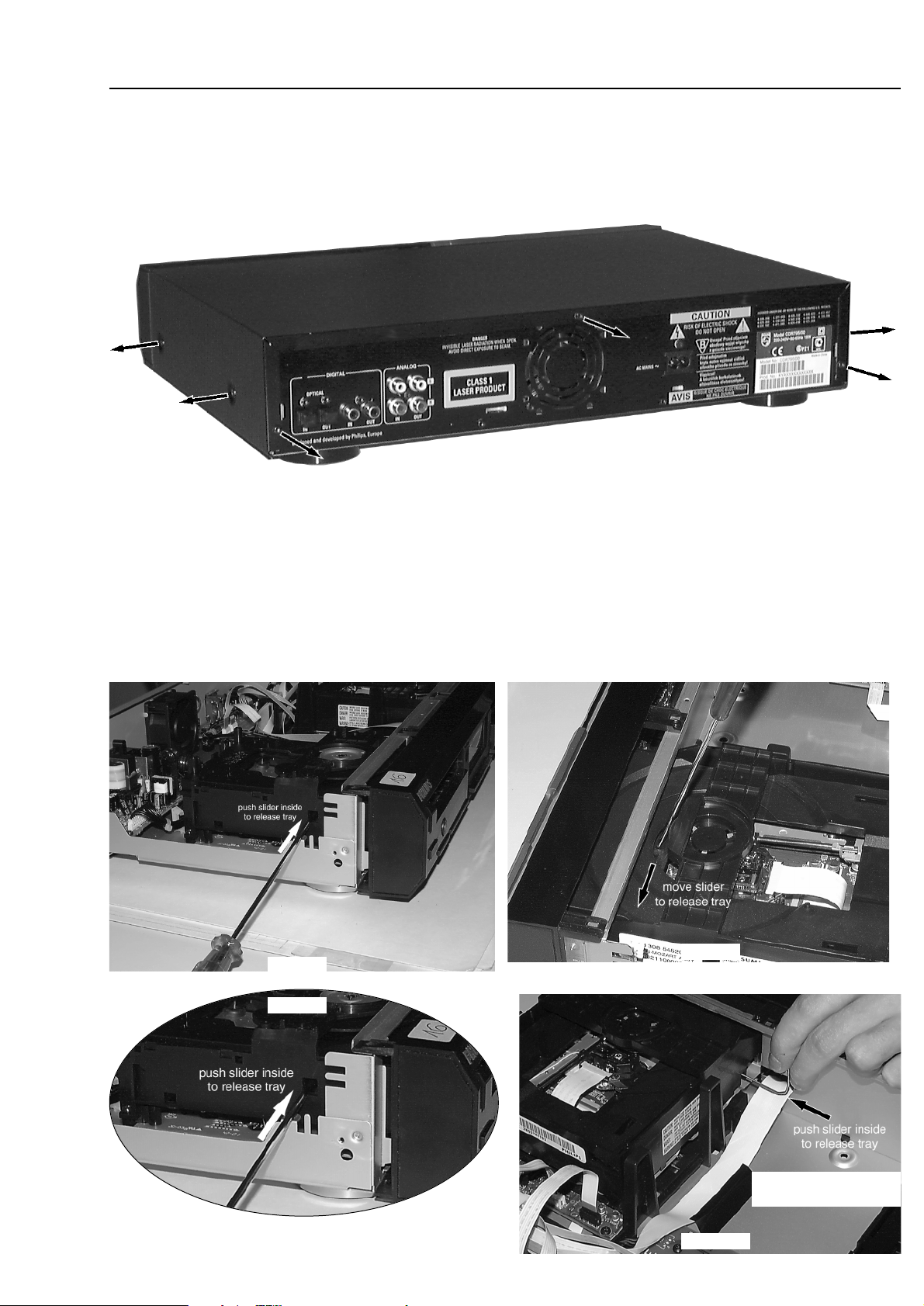
DISMANTLING INSTRUCTIONS
Dismantling the
Top Cover
picture 2
• Remove 7 (9) screws as shown in picture 2.
• Raise top cover at the rear and pull it backwards.
remark: in some production batches the top cover
may be fixed with 5 screws at the rear side.
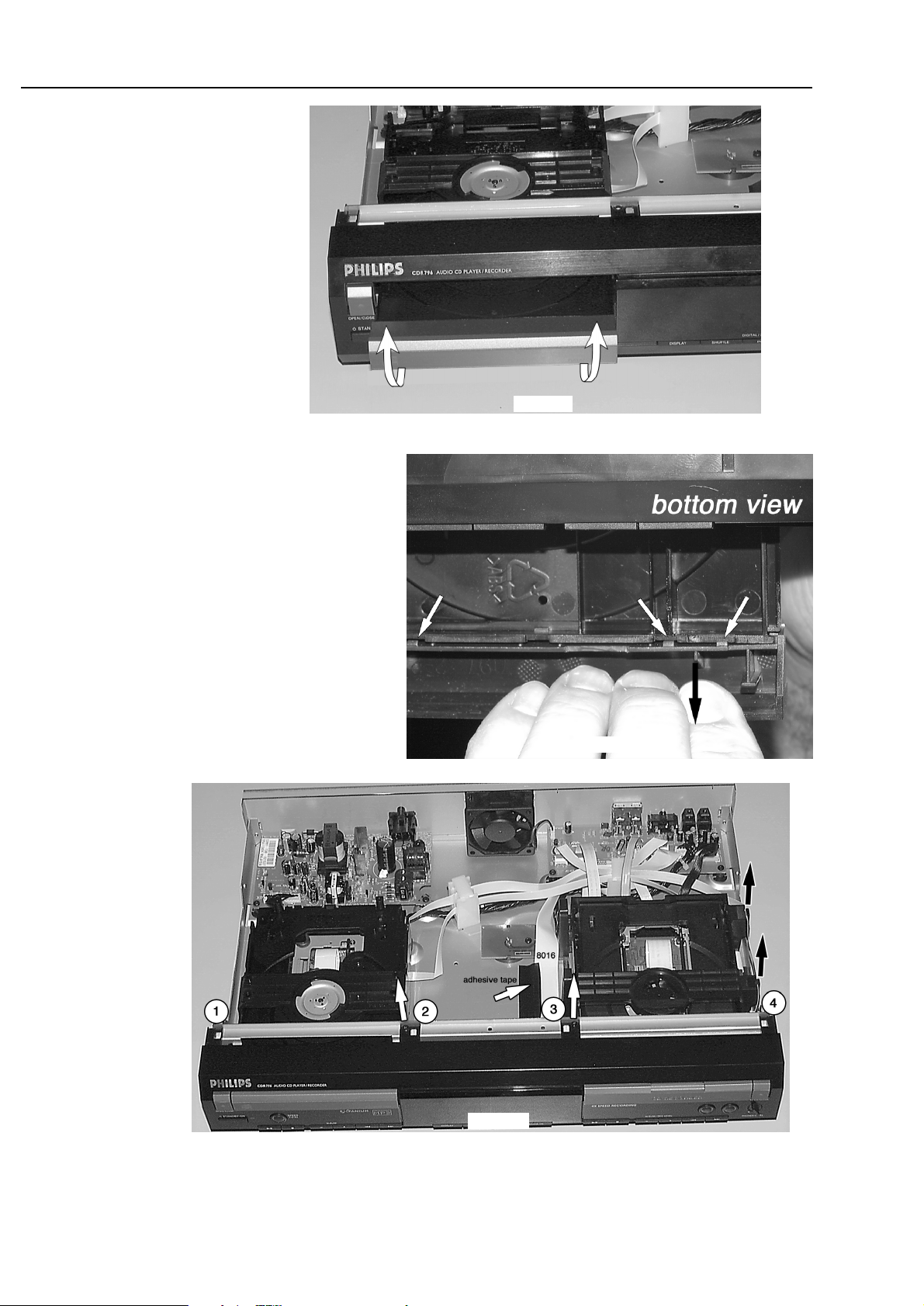
Dismantling the
Tray Covers
To dismantle the ornamental cover, the tray has to be moved out first.
This can either be done by activating the Open/Close-key or manually.
In order to avoid unnecessary loading it is recommended to move the tray out manually a few centimetres.
To release the tray manually proceed as shown in pictures 3, 4, 5 and 6. The tray will move out a little.
Afterwards it can be pulled out as far as convenient.
Release tray of CD Loader Release tray of CDR module
picture 4
picture 5
detail
picture 3
picture 6
or
use a short screwdriver
or a paper clip
Page 10
4-2
DISMANTLING INSTRUCTIONS
Dismantling the
Front Cabinet
picture 9
• Remove top cover and ornamental covers from the trays first →see description above and on page 4-1.
• Move trays back to
closed
position.
• Loosen 2 screws as shown in picture 9.
• Remove adhesive tape from cable 8016 and take cable to Headphone Board out of its guidings on the right
side of the CDR support.
• Release 4 catches on top (as shown in picture 9) first, then 2 catches on bottom (see picture 10).
• To release the cover from the catch on the tray, pull it
frontwards on bottom side as shown in picture 7 and 8.
• Pull the cover up.
picture 7
Dismantling the
Tray Covers
continued
picture 8
Dismantling the ornamental cover
from the
CDR-tray
functions in the same manner.
Page 11

4-3
DISMANTLING INSTRUCTIONS
Dismantling the
Front Cabinet
continued
picture 12
picture 10
picture 11
• Pull front cabinet forwards.
As the lug fits very tight in the bottom it is recommended to
make use of a screwdriver (see picture 11).
• Place front cabinet as shown in picture 12.
Page 12
4-4
DISMANTLING INSTRUCTIONS
• For proper mounting it is necessary that the pins
on the front side (see picture 14) are put into the
feed holes on the front cabinet ( see picture 15).
• Move the module frontwards until the guiding pins
at the rear slip into the holes on the bottom.
• Fix the module with 2 screws at the rear
(see picture 13).
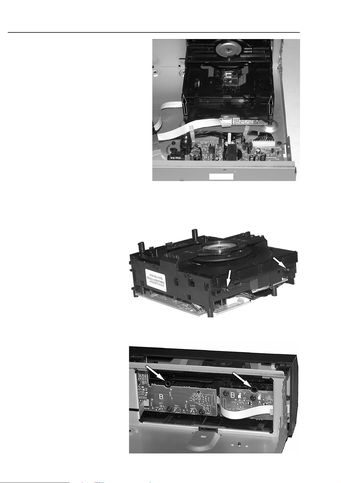
Dismantling the
CD module
• Remove top cover and ornamental cover from the tray first
→ see description on pages 4-1 and 4-2.
• Loosen 2 screws at the rear side →see picture 13.
• Move the complete module backwards.
• Pull the module on rear side up and turn it out.
• Put the module to a proper service position.
→ see also chapter SERVICE HINTS.
picture 13
picture 14
picture 15
Mounting the
CD module
Page 13
4-5
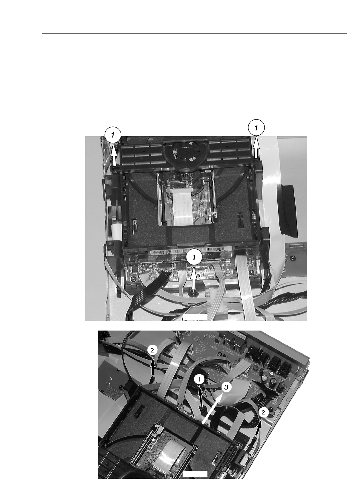
DISMANTLING INSTRUCTIONS
Dismantling the
CDR module
• Remove top cover and ornamental cover from the tray first
→ see description on pages 4-1 and 4-2.
• move tray back to
closed
position.
• to dismantle the complete module:
-loosen 3 screws to bottom cabinet (see picture 16
1)
-disengage catches (see picture 17
2)
-move module backwards
3 until catches to bottom cabinet
become free and pull it up.
picture 16
picture 17
Page 14
4-6
DISMANTLING INSTRUCTIONS
Dismantling the
CDR module
continued
• to dismantle the Loader module:
-move tray completely out.
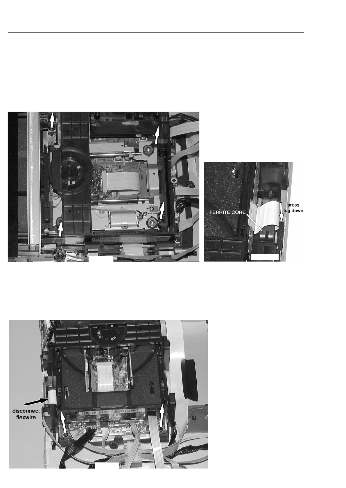
-loosen 4 screws to frame as shown in picture 18.
attention: flex wire to Mozart Board is too short for simple fetching the loader out. It is advised either
to dismantle the complete module as described on page 4-5 and to move it a few centimetres back
or to loosen ferrite core as shown in picture 18a.
- put the module to a proper service position.
→ see also chapter SERVICE HINTS.
• to dismantle the MOZART Board:
-loosen 2 screws to frame as shown in picture 19.
-unlock flex foil connector and disconnect flex wire.
-pull the board out of it´s guidings (backwards).
- place the Mozart board to a proper service position.
→ see also chapter SERVICE HINTS.
picture 19
picture 18
picture 18a
Press locking lug with a screwdriver down
and move ferrite core out of its guiding.
Turn ferrite core up and move it gently
along the cable.
Page 15

4-7
DISMANTLING INSTRUCTIONS
Dismantling the
Power board
• Remove top cover first →see description on page 4-1.
• Loosen 3 screws as indicated in picture 20.
• Move the board backwards to release the mains socket.
• Lift it on the rear and turn it out.
picture 20
!!
Attention: to fulfil safety requirements after repair it is
absolutely necessary to fix the cables as in
its original condition. See picture 21.
picture 21
Page 16

4-8
Dismantling the
Interface Board
• Remove top cover first →see description on page 4-1.
• Loosen 2 screws from the board and 4 screws from sockets at the
rear plate.
• Move the Interface board backwards to release the sockets and
turn it out (if necessary disengage cable guide).
• place the Interface board to a proper service position.
→ see also chapter SERVICE HINTS.
picture 22
DISMANTLING INSTRUCTIONS
picture 23
Page 17

SERVICE HINTS
5-1
SERVICE TOOLS
TORX T10 screwdriver with shaftlength 150mm ......................................4822 395 50423
TORX screwdriver set SBC 163 ..............................................................4822 295 50145
Audio signal disc SBC 429......................................................................4822 397 30184
Playability test disc SBC444...................................................................4822 397 30245
Test disc 5 (disc without errors) +
Test disc 5A (disc with dropout errors, black spots and fingerprints)
SBC 426/426A ....................................................................4822 397 30096
Burn in test disc (65 min. 1kHz signal at -30dB level without "pause") ...4822 397 30155
HANDLING CHIP COMPONENTS
DEALER MODE
The sets are equipped with a special DEALER MODE.
This mode blocks the trays of the CD - and CDR module to
prevent customers from fetching out CDs from exhibition
sets.
The Dealer mode can be switched on/off as follows:
1) Switch the set with the Remote Control to [Standby]
2) Press the
[DISPLAY] key at least for 5s
→ Display shows
TRAYS LOCKED else UNLOCKED
DEMO MODE
The DEMO MODE displays various features of the set and
will start automatically when no key has been pressed for
several minutes or during Standby mode.
The Demo mode can be switched on/off as follows:
1) Switch the set with the Remote Control to [Standby]
2) Press the
[STOP] key on the set at least for 5s
→ Display shows
DEMO ON else DEMO OFF
Page 18

5-2
SERVICE HINTS
General Service position
For measurements on: Power Board
Intrface Board
For manual release of: CD tray
CDR tray
Service position
Front Board
For dismantling instructions see chapter 4-1 to 4-3
picture 24
picture 25
Page 19

5-3
SERVICE HINTS
Service position
CD Module
picture 27
picture 26
picture 28
For dismantling instructions see chapter 4-4.
Page 20

5-4
picture 29
Service position
MOZART Board
(Back-end)
picture 30
picture 31
SERVICE HINTS
For dismantling instructions see chapter 4-6.
Service position
CDR Module
For dismantling instructions see chapter 4-5.
component side
copper side
Page 21

5-5
SERVICE HINTS
Service position
Power Board
picture 32
For dismantling instructions of the top cover
see chapter 4-1.
All important measurements can be carried
out from the component side without any
further dismantling.
Service position
Interface Board
picture 33
For dismantling instructions of the top cover
see chapter 4-1.
Component side is now accessible without
any further dismantling.
picture 34
To get access to the copper side the board
has to be dismantled and turned to service
position as shown in picture 34.
For dismantling instructions see chapter 4-8.
Page 22

5-6
SERVICE HINTS
Personal Notes:
Page 23

5-75-7
N
Y
KEY TEST
Display shows
Numbers acc. table 2
are indicated as long as a
button is held depressed.
If a button is pressed
on the Remote Control
KEY RC is shown
and the ; flag flashes.
CD
ALBUM -
button
pressed?
CD
STOP
button
pressed?
N
Y
10SHUFFLE
INPUT
ALBUM -
(CDR)
PLAY/PAUSE
(CD)
SPEED
STOP
(CDR)
19
20
21
PLAY/PAUSE
(CDR)
RECORD
KEY KEY CODE
2
3
4 (exit)
5
6
7
8
9
12
15
11
S
(CDR)
ALBUM +
(CDR)
14
13
16
17
ERASE CD
S
(CD)
STOP
(CD)
ALBUM -
(CD)
STANDBY
T
(CDR)
OPEN/CLOSE
(CD)
18
T
(CD)
1
0
ALBUM +
(CD)
DISPLAY
COPY CD
OPEN/CLOSE
(CDR)
KEY KEY CODE
KEY CODES
table 2
SERVICE TESTPROGRAM
VARIOUS TESTS
CDR79x servtest various, 240402
N
Y
FORMAT EEPROM
Display shows
for 2s.
EEPROM is cleared and
default values are stored.
SHUFFLE
button
pressed?
This test should only be used to clear
the EEPROM in case of a µP-"hangup".
Attention: all data are set to default values,
BLACK BOX data are not cleared.
KEY --
DISPLAY
button
pressed?
STOP
button
pressed?
N
N
Y
Y
Display shows
all
segments and flags
for checking open circuits.
see figure 1
All LEDs are switched on.
DISPLAY TEST
fig. 1
N
Y
QUARTZ TEST
Display shows
1220±37Hz can be measur.
on (pin 23 of µP).
STOP
button
pressed?
N
Y
SPEED
button
pressed?
Tact frequency µP
(divided 10MHz)
f
0
10M
NEW
VXX
S
*
To leave Service Testprogram plug mains cord off.
*
In the main menu the sound settings (volume, ...)
and trays work as in normal mode.
Display shows
version number
of the µP - software.
stands for Service mode
stands for Version number
of the software used in the
Front (Display) µP.
To enter Service
Testprogram hold
PLAY & REC
buttons
depressed while
plugging mainscord in.
S-CDR795-VXX
NY
EXIT
END-USER DIAGNOSTICS
Display shows:
FAILED
for 3s.
Display shows:
PASSED
for 3s.
END-USER DIAGNOSTICS
(CDR module)
To enter
END-USER DIAGNOSTICS
hold S & T buttons
on CDR side depressed
while plugging mainscord in.
TEST O.K.?
Display shows for 5s each:
• Software version of
set µP
S
stands for Service mode
VXX
stands for Version
number of the software used
in the Front (Display) µP.
• Software versions of the
CDR module:
MOXXXX
stands for
Software version of
MOZART flash ROM 7101
BXXXX
stands for
Software version of
Basic Engine
flash EPROM 7017
SDRAM TEST 7100
Display shows:
DTST1
CHECKSUM TEST 7101
Display shows:
DTST2
ERASE TEST 7101
Display shows:
DTST3
COMMUNICATION TEST
(UART-BUS)
Display shows:
DTST4
S-CDR795-VXX
MOXXXX BXXXX
NEW
Display shows
for 2s.
EEPROM is cleared
and default values
are stored.
PASS
N
Y
EEPROM TEST
Display shows
ERR
Display shows
Testpattern is written to
address 1
and
read back again
INPUT
button
pressed?
STOP
button
pressed?
Test ok?
N
Y
N
Y
NTC XX
N
Y
TEMPERATURE
(NTC) TEST
Display shows
XX = value in °C
STANDBY
button
pressed?
STOP
button
pressed?
N
Y
STANDBY
button
pressed?
N
Y
Fan is switched on/off
display shows
or
for 2s.
FAN ON
FAN OFF
STEP ALBUM MP3PLAYLIST TOTAL REM REC TRACKTRACKTIME TIME
REP TRACK DISC ALL PROG SHUFF
CDTEXT
EDIT
CD RECORDER
L
R
CD PLAYER
8X4X
2X1X
LINEDIG
OPTMIC
REC
CD RW
FINALIZE
SERVICE TESTPROGRAM
VARIOUS TESTS
Page 24

5-8 5-8
CDR
DC-ERASE MODE
SERVICE TESTPROGRAM
CDR MODULE
DC-ERASE
finished?
N
Y
BURN IN MODE
CDR MODULE
Display shows:
HH BI RE FE
DC-ERASE MODE
starts.
Record complete disc
from analog source
with normal speed.
Display shows:
HH BI RE FE
Complete disc
recorded?
N
Y
Error detected?
N
Y
Finalize disc
with double speed.
Display shows:
HH BI RE FE
HH stands for the number of hours
the test was running
BI stands for Burn In test
RE number of errors detected during
DC erase and write mode
FE number of errors detected during
Finalizing the disc
CDR79x servtest CDR module, 240402
Y
Disc erased?
N
Y
N
Y
Complete disc will be
erased with 4x speed.
(starting from PMA-area
up to and including
ATIP leadout area)
The display shows the
countdown of the
remaining time required
to complete the operation:
ER mm ss
Display shows:
PASSED
mm: remaining minutes
ss: remaining seconds
STOP
button
pressed?
Exit DC-ERASE Mode
Note: With the DC-Erase mode the CD-RW can be
changed back in its original state, like a new disc.
Stopping the erase-function by switching power off
will leave the disc in an unpredictable status!
TEST O.K.?
NN
Y
YY
CDR
ELECTRICAL TEST
Insert CD-DA disc
before starting the test
MODULE INFORMATION
MOZART BOARD DIAGNOSTIC
CDR - LOADER TEST
SDRAM TEST 7100
Display shows:
DTST1
CHECKSUM TEST 7101
Display shows:
DTST2
ERASE TEST 7101
Display shows:
DTST3
COMMUNICATION TEST
(UART-BUS)
Display shows:
DTST4
Display shows:
DERR
n
n=number of failed test
Display shows next error
CDR
T button
pressed?
N
Y
Y
Y
all errors shown?
N
N
N
TEST O.K.?
NN
Y
Y
Display shows:
BERR 1
Display shows:
PASSED
for 3s
The test is performed by
playing 5s at beginning,
5s in the middle and 5s at
the end of the disc.
Display shows actual
playing time.
Note: The BURN-IN mode is an endless cycle of
*
DC erase, to erase the CD-RW disc with max. laser power
*
Recording a CD-RW disc with speed N=1
*
and Finalizing with double speed
This test is intended to check the quality of a CDR loader and
to detect intermittent failures.
Exit CDR electrical Test Exit CDR electrical Test
Display shows for 5s:
MO XXXX BXXXX
• MO xxxx stands for
Software version of
MOZART
(flash ROM 7101)
• Bxxxx stands for
Software version of
Basic engine processor
(flash EPROM 7017)
CDR
T button
pressed?
CDR
T button
pressed?
CDR
T button
pressed?
CDR
T button
pressed?
S
*
To leave Service Testprogram plug mains cord off.
*
In the main menu the sound settings (volume, ...)
and trays work as in normal mode.
Display shows
version number
of the µP - software.
To enter Service
Testprogram hold
PLAY & REC
buttons
depressed while
plugging mainscord in.
S-CDR795-VXX
CDR
ALBUM +
button
pressed?
N
Y
ERASE CD
button
pressed?
N
Y
RECORD
button
pressed?
N
Y
VXX
stands for Service mode
stands for Version number
of the software used in the
Front (Display) µP.
SERVICE TESTPROGRAM
CDR MODULE
Page 25

5-95-9
SERVICE TESTPROGRAM
CD MODULE
CDR79x CD servtest, 240402
OPEN/CLOSE
button
pressed?
N
Y
N
Y
CD
PLAY
button
pressed?
N
Y
CD
MECHANICAL TEST
SLIDE TESTFOCUS TESTTRAY TEST TURNTABLE
TEST
Display shows:
SLIDE
for visual inspection only
OPEN/CLOSE
button
pressed?
N
Y
Y
N
Y
N
Slide moves
continuously in/out.
Display shows:
CD ME TEST
Display shows:
OPEN
(even when tray is blocked)
Tray opens.
Display shows:
CLOSE
(even when tray is blocked)
Tray closes.
Slide moves to inner
position.
N
Y
STOP
button
pressed?
Exit CD Mech. Tests
Objective moves
continuously up/down.
Display shows:
FOCUS
N
Y
CD
ALBUM -
button
pressed?
CD
ALBUM +
button
pressed?
N
Y
Turntable motor
is switched on.
Display shows:
DISC
Focus servo
is switched off.
Turntable motor
is switched off.
Move slide manually backwards to get view of the pickup.
It is recommended to enter the mech. tests
in the sequence as drawn below.
Otherwise it might happen that the one
or the other test will not be activated electrically.
2)
2)
2)
CD
PLAY
button
pressed?
CD
ALBUM -
button
pressed?
CD
ALBUM +
button
pressed?
CD
LOADER TEST
TEST O.K.?
NN
Y
Y
Display shows:
BERR 1
Display shows:
PASSED
for 3s
CD
T button
pressed?
The test is performed by
playing 5s at beginning,
5s in the middle and 5s at
the end of the disc.
Display shows actual
playing time.
N
Y
CD
ALBUM +
button
pressed?
Exit CD electrical Test Exit CD electrical Test
Insert CD-DA disc
before starting the test
VXX
S
*
To leave Service Testprogram plug mains cord off.
*
In the main menu the sound settings (volume, ...)
and trays work as in normal mode.
Display shows
version number
of the P - software.
stands for Service mode
To enter Service
Testprogram hold
PLAY & REC
buttons
depressed while
plugging mainscord in.
S-CDR795-VXX
CD
S button
pressed?
N
Y
stands for Version number
of the software used in the
Front (Display) P.
SERVICE TESTPROGRAM
CD MODULE
Page 26

6-1 6-1
1307
1310
17
1304
51
1303
71
1309
15
7324F
74LVU04D
+IC
1314B
DIG IN
7312
OPT. IN
1315B
+F
+12V
-F
-30V
+5V
+5V
+5V EVER
+F
-F
-30V
+5V EVER
+12V
+5V +ICV_AMP1+ -12V
0054
16
V_AMP1-
HP_L
HP_R
ANA IN_R
ANA OUT_L
EBU IN COAX
ANA OUT_R
ANA IN_L
-12V
+12V
LM833D
V_AMP1+
V_AMP1-
1315A
1314A
DIGITAL
OUT
7324E
74LVU04D
+IC
7324A-D
5300
7320
74LVU04D
+IC
+5V
1306
13
1391
13
1301
12
NTC
10k
FAN
FAN CONTROL
provisional
INTERFACE BOARD
ANALOG
OUT
LINE IN
15 1
1308
91
POWER_ON
POWER_ON
FAN
UL SW Info
NTC
EBU IN OPT.
EBU OUT
+5V
NC
NC
+12V
+5V
+5V
+12V
LEVEL SHIFT
BUFFER
UL_SW Info
UL_DRAWER OUT
UL_DRAWER IN
UL_SPEEDSELECT
UL_DRAWER OUT
UL_DRAWER IN
UL_SPEEDSELECT
7313
OPT.OUT
CON1
CN101
12 1
8
1
(Supply) ON/OFF
+5V EVER
-F1
+F1
-30V
+5V
+12V
EBU IN CD10
+5V
AUDIO SIGNAL INTERFACE
DIGITAL IN / OUTCONTROL INTERFACE
SUPPLY INTERFACE
CD INTERFACE
RESET CD10
CD10 SDA
CD10 SCL
CD10 RAB
CD10 SILD
-12V
CD - MODULE
for details see
separate block diagram
SWITCHED MODE
POWER SUPPLY
for details see
separate block diagram
CDR MODULE
for details see
separate block diagram
HEADPHONE-
MICROPHONE
BOARD
14021007 1203
1205
176115
1501
+12V
-12V
HP_L
HP_R
7500
3502
+12V
-12V
NJM4556AM
HEAD-
PHONE
I2C DATA
I2C CLK
RESET
EBU OUT
EBU EXT. IN
EBU IN OPT.
ANALOG IN (REC) L
ANALOG IN (REC) R
ANALOG OUT (PB) R
ANALOG OUT (PB) L
8
1
SPDIF (EBU)
CD10_RESET
SDA
SICL
RAB
SILD
1802
IRQ
1805
91
SW Info
+5V
RIGHT
SDA
+10V
1214
16
+5V
+5V
+12V
TRAY OUT
TRAY IN
SPEEDSELECT
1503
1505
OPEN/CLOSE
CDR
12
KEY2·
16
1316
61
1500
CDR79x, 080502
DISPLAY BOARD
LIGHTGUIDE BOARD
KEY BOARD
7414
7409
7406
7416
6429
6431
MICROPROCESSOR
M30218MAFP
7403
7450 7451
6450 6451
7405
7402
5VST
+5VST
+5V
RC5
KEY 1
KEY 0
KEY 2
2
KEY MATRIX
RESET
EEPROM
RESET
1416
1414
1
4
4
1
1460
-30V
+F-F
-30V
3V3
1
3
30
40 - 881689
63
VCC1
VCC2
99 VREF
100 AVCC
97AVSS
65VSS1
14VSS2
VEE
1400
10MHz
13929190 15
12
+5VST
I2C DATA CDR
I2C CLK CDR
+P
+P
+5V
23
1
1, 2 54, 55
3
4
2
21
19
20
5
8
6
LED Drawer CDR
LED Drawer REC
LED Copy
LED REC
LED red
LED blueLED blue
REC COPY
LED red
+5V
+5V
+5V
blue
Rec/Pb indication
red
+5V
66
1
KEY0·
KEY2·
KEYKEY
KEY
KEY
KEY0·
LED ON/OFF
LED SpeedLED Speed
IR EYE
0060
1
LED ON/OFF
POWER_ON
NTC
f
0
1418
+F -F
-30V +5V +5VST
FAN
PDWN
UL_SW Info
UL_DRAWER OUT
UL_DRAWER IN
UL_SPEEDSELECT
IRQ CDR
IRQ CDR
RESET CDR
I2C CLK CDR
RESET CDR
I2C DATA CDR
1417
+5VST
+P
+P
STANDBY SPEED
KEY MATRIX
15 11 6
I2C BUS
+5V
1415
12
+5V
STEP ALBUM MP3PLAYLIST TOTAL REM REC TRACKTRACKTIME TIME
REP TRACK DISC ALL PROG SHUFF
CDTEXT
EDIT
CD RECORDER
L
R
CD PLAYER
8X4X
2X1X
LINEDIG
OPT MIC
REC
CD RW
FINALIZE
I2C BUS
BLOCK DIAGRAM
Page 27

6-26-2
MOZART
IC
CORE
SUPPLY
I/O
SUPPLY
SUPPLY
SUPPLY
PLL
OSC
JTAG/BDM
SDRAM
2MB
1MB
FLASH
CONTROL
ADRESS
DATA
CONTROL
EBUIN2
I2S
1 IN/OUT
/2
74LV74D
MCF5248
7100
7101
7000
7004
DC/DC
7201
DAC ADC
OPAMP
circuitry
Potmeter
ANALOG
SWITCH
3
I2S2 I2S3
3
7312
7301
7401
7402
7311
7300
16
20
8
3
DC/DC
6204
GND
DC/DC
DC/DC
DC/DC
DC/DC
7202
7200
7208
7209
+5V
+12V
3V3
2V5
-12V
-8VA
-5VA
-8VA
SPDIF / EBU1 (PB)
Reset CD10
SDA,SICL,Rab, Sild
PWR ON RST
CLK 16
PLAYBACK
ROUTING
FREYA EAN
FREYA EAN
Mute, Attenuation, Deemphasis
RS232
CD TEXT
I2S1(in/out)
EBU2 (Pb)
1201
1205
1214
C
D
M
O
D
U
L
E
OPAMP
circuitry
7401
7400
7400
1203
1215
13051304
1402
1303
+5VA
+8VA
"MOZART" BOARD CDR2001
EBU Dig_Opt Out
EBU4 Ext INI
Pro Dig Out
EBU3 opt IN
EBU3 COAX
BUFFER
ADC CLKDAC CLK
ZERO
A_Left_In
A_Right_In
A_Out_Left
A_Out_Right
+8VA-8VA
INTERFACE BOARD
D
I
S
P
L
A
Y
B
O
A
R
D
I2C
IRQ FRONT
VCXO
FILTER
Xtrim
CLK 33,86MHz
2V5
GND 3V3
3V3 3V3
GND
GND GND
1007 1417
1 23
4
5
5
6
FLEX
36p
FLEX
8p
FLEX
17p
FLEX
7p
+5V
IO CLK 16
I2S
1
KILL
I2S
4
PWR ON RST
MUTE, ATT,
DEEMP.
EBU EXT INI
EBU EXT INI
EBU DIG
OPT OUT
PRO DIG OUT
EBU IN FREYA
PWR ON RST
I2C
IRQ FRONT
2
4
4
3
4
3
FREYA CLK
2
7010
Kill
KILL
circuitry
7002
1005
B
A
S
I
C
E
N
G
I
N
E
Mute,
Deem-
phasis
Kill out
FLEX
CONTROL
INTERFACE
AUDIO SIGNAL
INTERFACE
SEPARATE AD/DA
INTERFACE
DIGITAL
INTERFACE
6p
I2S4 IN
EBU DIG
OPT OUT
OPAMP
circuitry
6202
CD R/W
I2S
INTERFACE
Mozart CDR79x, 010402
1802
COPY ANALOG
0054
BLOCK DIAGRAM
CDR MODULE
Page 28

6-3 6-3
5
6
3
4
2
8
7
RAB
1802
RESET
SDA
SPDIF
GND
1
GND
Communication CD10
with CDR Module-µP
Digital Audio
SICL
SILD
SPEEDSEL
Low = 4x speed
Low = 2x speed
High = 1x speed
High amplification
(4x speed)
Low amplification
(1x and 2x speed)
CDR Version
VAM2201, VAM2202, VAM2204
7802
7803
V5EQSEL
62
12
1805
6
7
8
9
2
3
4
5
1
NC
NC
38
RESET
SPEEDSEL
SPEEDSEL
Control
CDR Version
to CDR Module
1205
to Interface Board
1308
SDA
VCC
DOBM
D1-D5
D2-D4
1806
LD ONLD ON
LD
MON
CD/RW
HF IN
V1
D1
D2
D3
D4
R1,R2
MOT1
SIGNAL PROCESSOR
CD10
SAA7324 (SAA7325)
TRAY
MOTOR
SL
RA
FO
DIODES
PHOTO
D3D2
D5D1
D4
INNER SWITCH
SW INFO
TRAY OUT
TRAY IN
LASER &
MONITOR
DIODE
TURNTABLE
MOTOR
DISC
CD MECHANISM
TRAY
MAINBOARD
7801
+3,3V
7802
LASER CONTROL
&
HF AMPLIFIER
TZA1024
(TZA1025)
42
40
39
5,17,21,52,57
64
1
13
+5V
+8V
2
+8V
16,17,20
4
5
7
V4
61
2
ISLICE
3
63 51
8
7
6
2
5
1
3
11
6,14
6...12
25...31
4
2
1
4
3
2
1
4
3
+3,3V
SCL
SILD
Blockdiagram Universal Loader 2002 02 12
+5V
+3,3V
7816
+5V
+A
+8V
7820
6802
BLOCK DIAGRAM Universal Loader
FOCUS
MOTOR
RADIAL
MOTOR
SLIDE
MOTOR
MOTOR
TURNTABLE
55
54
56
59
34
32
33
5
4
13
14
23
24
3
15
19
7819
M63000
DISC+
DISC-
SLI-
SLI+
TRA-
TRA+
FOC-
FOC+
MOT2
6021
1830
Standby
36
TRAY
SWITCH
REF (3,2V)
+5V
TRAY OUT
SW INFO
TRAY IN
TRAY OUT
SW INFO
TRAY IN
+10V
GND
Supply
7815
TCA0372
10
41
RAB
BLOCK DIAGRAM
CD MODULE
Page 29

6-46-4
D207
Q202
BLOCK DIAGRAM
SWITCHED MODE POWER SUPPLY /
European & USA version (/00 & /17)
CN101
MAINS SOCKET
F101
T2A
Lightning
Protection
L101, L102
EMI-filter
T102
6,8V
22V
+5V EVER
overvoltage
protection
Q151
PC151
PC102
switch on/off
regulation
regulation
IC251
D251
D252
Q152
R152
C105
C251
D201
D206
C206
CON1
1
12
ON/OFF
+5V EVER
+F1
-F1
-30V
+5V
+12V
-12V
Q251
Q202
22V
T101
27V
+12V
overvoltage
protection
C208
D203
C204
-12V
C202
D202
C201
+5V
+5V
IC201
Q101
Q104
on/off
switching
transistor
reference
PC101
Q103
R222
R209
D204
D208
C205
-30V
+F
-F
switching
transistor
reference
Blockdiagram SMPS CDR8xx, 040901
BLOCK DIAGRAM
POWER SUPPLY
Page 30

6-5 6-5
LED_red
FFC SIDE ENTRY
EH TOP ENTRY
EH SIDE ENTRY
DIPMATE
BOARD to BOARD JQ
FFC TOP ENTRY
LEGEND
PH TOP ENTRY
PH SIDE ENTRY
XH SIDE ENTRY
FLASH TOP ENTRY
FFC TOP ENTRY
CABLE 1 to n
1mm PITCH
FFC SIDE ENTRY
1mm PITCH
1203
+F
-F
-30V
+5Vever
ON/OFF
+12V
+12V
GND
GND
+5V
+5V
-12V
112
CON1
GND
CD10 SDA
CD10 SICL
CD10 RAB
CD10 SILD
Reset CD10
EBU IN CD10
EBUGND
1802
+5V
EBUOUT
EBUINOpt./GNDD
EBUINCoax
GNDD
5
ANA OUT LEFT
GND A
ANA OUT RIGHT
GND A
ANA IN RIGHT
GND A
ANA IN LEFT
171618
1402
+5V
+5V
GNDD
GNDD
GNDS
+12V
6
1214
GNDD/Shield
I2C-Data
GNDD
I2CClock
Reset
IRQREQ
11
1007
GND
SDA
SICL
RAB
SILD
CD10_RESET
SPDIF(EBU)
SPDIFGND
1
8
1205
(SDA)
Speed_select
TRAY IN
TRAY OUT
SW_INFO
+10V
GND
+5V
(RIGHT)
91
1805
1416
1
6
GND
I2C_Data
GND
I2C_CLK
Reset
IRQ CDR
16
1417
UL_Speedselect
UL_Drawer_in
UL_Drawer_out
UL_SW_INFO
PDWN
Fan
Power_ON
GND
GND
+5V_ever
+5V
NTC
-30V
-F
+F
115
1
4
1
4
1418
Flash_TxD
Flash_RxD
Flash_SCLK
Flash_BUSY
Flash_VPP
GND_D
RESET
+P
1
flash connector
8
1413
+5V
+5V
LED_blue
GND
1414
LED_blue
LED_red
GND
1460
HP RIGHT
+12V
HP LEFT
-12V
GND
GND
1500
0060
8007 (480mm)
HR(5p+7p)-HR12p
10x twisted
8004 (140mm)
OP-PH/6p
CD R/W MODULE 2001
MOZART BOARD
componentside view
KEY BOARD
copperside view
HEADPHONE
BOARD
componentside
view
SWITCHED MODE
POWER SUPPLY
componentside view
6
1
1
LIGHTGUIDE BOARD
copperside view
CD MODULE
UL-CDR/MP3/BASIC
MAIN BOARD
componentside view
LED ON/OFF
LED SPEED
GND_Key
Key 0«
+5V
GND_D
LED ON/OFF
LED SPEED
GND_Key
Key 0«
+5V
GND_D
1
6
8012 (340mm)
1
2
1415
Key 2«
GND
Key 2«
GND
1503
8017 (140mm)
HR-HR/2p
13141315
NTC
HP RIGHT
+12V
HP LEFT
-12V
GND
GND
NC
UL_Speedselect
UL_Drawer_in
UL_Drawer_out
UL_SW_INFO
+10V
GND
+5V
NC
1308
+5V
EBUOUT
EBUINOpt./GNDD
EBUINCoax
GNDD
15
7 13
1306
13
1391
ANA
OUT LEFT
GND A
ANA OUT
RIGHT
GNDAANA IN RIGHT
GND A
ANA
IN LEFT
116
19
1303
1316
+5V
+5V
GNDD
GNDD
GNDS
+12V
16
0054
UL_Speedselect
UL_Drawer_in
UL_Drawer_out
UL_SW_INFO
+5V
Fan
Power_ON
GND
GND
GND
+5V_ever
+5V
NTC
NTC
-30V-F+F
115
1307
+F
-F
-30V
+5Vever
ON/OFF
+12V
+12V
GND
GND
+5V
+5V
-12V
1715
1310
1309
1
1301
7313 7312
Optical
IN
Optical
OUT
Digital
IN/OUT
Line
IN/OUT
8009 (180mm)
HR-HR/3p
1304
FAN
INTERFACE BOARD
componentside view
DISPLAY BOARD
copperside view
8016 (360mm)
FFC1,25/15p/ AD
8008 (340mm)
FFC1,25/6p/BD
8001(140mm)
PH-PH/5p
8003 (140mm)
FFC1,25/7p/BD
8015 (340mm)
FFC1,0/ 8p/ AD
8014 (360mm)
FFC1,25/9p/ AD
wiring diagram CDR79x, 080502
FFC1,25/6p/ BD
8006 (60mm)
FFC1,0/ 4p/ BD
8005 (120mm)
FFC1,25/6p/ AD
WIRING DIAGRAM
For service code numbers of flexfoil cables see mechanical partslist.
Page 31

7-17-1
-30,7V -29,2V
-29,9V
4,8±0,45V
floating
4,5/0V
5±0,25V
5±0,25V
12
+0,6
/
-1,2
V
-11,5
+1,5
/
-1,1
V
-29,3±2,2V
typ.-25V
typ.-20V
300V
300V
5V
5V
5V
4V
5V
4V
12V
-12V
-32V
-20V
-25V
2,5V
2,5V
1,2V
0V
4,5V
300V
1,9V
1,9V
0,1V
16,5V
-0,3V
0,2V
0,2V
1,1V
1,1V
6V
1,1V
. . . V DC VOLTAGES MEASURED IN
STOP MODE
UNLESS STATED OTHERWISE
MAINS VOLTAGE 230V (120V
USA
)
PRIMARY MEASURED AGAINST
JUNCTION D103/D104
EVM
V
Switched Mode Power Supply / EU + USA version (/00/17)
to Interface Board
0052/0053
.......
USA
for USA version only
LEGEND
Switched Mode Power Supply, EU+USA versions, 300701
(SRA1134EK+SRA1133UC combined)
EU version USA version
22
USA
470k
USA
470k
USA
2200pF
USA
10
USA
1000pF
USA
220/200
USA
33n/400
USA
100p/1k
USA
0,01/50
USA
2200p/50
USA
220/1
USA
180k
USA
27k
USA
18k
USA
180k
USA
30V
27V
22V
6,8V
3V
22V
for orientation only
POWER BOARD / copper side view
USA and European version
SMPS CDR8xx,EU+USA, 300701
SRA1134EK+SRA1133UC
R111
R202
R203
R210
R204
C110
C113
R153
R156
R256
R257
R252
R212
R213
R254R253
C207
C152
C153
C109
POWER BOARD / component side view
USA and European version
L102
L101
R101
C102
C101
CN101
Z101
F101
R114
R104
R106
Q103
Q101
D110
R102
R151
R155
Q152
Q151
R152
D151
D153
R103
D109
D203
R222(R221
USA
)
R201
IC201
D108
R117
R112
R115
D111
R120
C108
Q104
R108
C105
D101
D103
D104
D102
R158
T101
T102
R119
C11
R154
C111
PC151
PC101
PC102
D201
C201
C202
C203
L201
L202
D202
C208
C210
C205
C253
C211
C254
C251
IC251
L204
Q202
Q251
L251
R251
D207
R220
R255
CON 1
C206
L203
D208
D251
D252
D204
C204
D206
R205
R209
SMPS CDR8xx,EU+USA, 300701
SRA1134EK+SRA1133UC
Page 32

7-2 7-2
1427 F11
1428 I10
1429 F12
1432 H10
1433 I10
1434 F13
1435 F13
1436 G10
1438 F10
1439 G10
1441 G10
2410 E10
2411 D11
2412 E11
567
I2C_Data
DISPLAY BOARD
GND
IR EYE
8 9 10 11 12 13 14
3424 H8
3425 H6
3426 G7
1422 G11
1423 G11
1424 G11
1425 H10
1426 H10
E
F
G
I2C_CLK
GND
EEPROM
2400 H4
2401 H4
2404 F10
2405 F11
2406 D10
2407 D9
2408 E9
2409 E10
3455 H10
3456 H10
3457 I10
2413 A4
Flash connector for
RESET
34
2422 F12
2423 E12
2424 D12
GND
2426 D13
3400 B1
3401 C1
3402 C1
3403 C1
3404 C1
3405 C1
3406 F2
3408 D1
3410 D1
3412 D2
3413 D1
3420 G4
3421 H4
3423 G5
3505 I7
3427 H7
A
B
C
D
3434 G6
3435 H7
3436 H7
1007
from Headphone Board to/from CD-RW Module
3437 H7
3438 G3
3439 H3
3440 H3
3442 G9
3443 E9
3444 F9
3445 F9
3446 F9
3447 F9
3448 F9
3449 F10
3450 F10
3451 G10
3452 G10
3453 G10
3454 H10
7409 H1
7412 H12
7413 G13
3458 I10
2414 A9
2415 B11
2416 H1
2418 C11
2420 D12
3464 G11
3465 F12
3466 F12
IRQ
3467 F13
3471 D10
3472 E11
3473 E11
3474 A4
3475 A9
3477 I8
3478 I7
3479 H11
3480 G13
3484 I2
3485 I2
3486 I2
3487 I2
3488 B13
3494 F12
3495 H12
3496 G12
3499 F9
F423 C13
F424 C13
F425 C13
3506 I6
3428 H7
3429 G7
3430 F9
3431 H4
3433 G5
3517 H6
3518 H6
3519 H6
flash version of uP only
3520 H6
3521 F2
3522 F2
3523 F2
3524 F2
5400 B11
6400 A10
6429 I7
6431 I8
6434 F9
7402 A9
7403 H3
7405 D11
7406 I8
F453 H13
F454 G13
F455 H13
7414 B8
3459 I10
3460 F11
3461 F11
3462 G11
3463 G11
F404 F3
F405 G3
F406 A9
0060
GND
1503
10MHz
F407 D9
F408 E9
F409 H4
F410 A4
F411 G4
F412 A13
F413 A13
F414 A13
F415 A13
F416 A13
F417 B13
F418 B13
F419 B13
F420 B13
F421 B13
F422 B13
F426 G5
3508 E2
3509 E2
3510 D10
3513 H1
3516 B11
F432 I6
F433 G11
F434 G10
LED SPEED
LED ON/OFF
1460
Key2«
to/from Interface Board
UL Speedselect
UL Drawer in
UL Drawer out
UL SW Info
+5V
F435 G10
F436 H10
F437 I7
F438 H10
F440 I10
F442 I10
F444 I10
F452 G13
F456 H13
7416 I6
F400 F2
F401 F3
F402 F2
F403 F3
F462 D13
F463 D13
F464 D13
+5V
REC
to/from Key Board
COPY
1307
F465 D13
F466 D13
F427 G4
F428 F10
F429 F11
F430 G10
F431 G11
F457 I13
F458 F13
F459 I13
F460 I13
F461 I13
Power Down
12
5678910111213143412
Reset
LED blue
LED red
H
I
E
F
G
A
B
C
D
H
I
1414 G13
1415 F13
1416 H13
1400 E9
1413 F1
1417 D13
1418 A13
6400
BZX79-B3V3
SHUFFLE
1439
1
2
3
4
5
6
1
2
3
4
5
6
7
8
FE-ST-VK-N
1417
1413
FE-BT-VK-N
D
100K
3442
3509
10K
10K
3508
10n
2410
D
65 14
10
11
1513
4
8
6
2726252423
302928
34
1663 8999 82 81
80
79
2221201918
17
12
33
735
4847
84
46454443424140393837
83
3635
64
62
61
60
59
58
578556
55
545352515049
87
78
77
76
75
74
73
72
71
70
698668
67
66
98 96 95 94 93 92 91 90 100
97 32931
1
2
88
7414
2412
1424
10n
1415
EH-B
1
2
1n
2404
3522
100R
3485
470R
100R
3523
3408
68K
D
F462
1K
3440
DISPLAY
1438
F444
F427
3466
270R
3467
390R
3475
10K
D
F460
F455
F453
100R
3521
F465
ERASE CD
1436
D
3516
2R2
F407
3427
470R
1428
<<
CDR
47p
2426
341268K
D
10K
3478
CSTS
1400
3420
1K
3524
100R
220R
3461
F422
D
3445
470R
D
68K
3410
150R
3480
COPY
1435
F414
+5V
BC847B
7416
3425
470R
3455
1K2
D
2423
47p
F410
4K7
3496
D
2
3
4
D
470R
3513
to_LIGHTGUIDE_PCB
FMN
1414
1
F405
3495
10K
GNDK2GNDK0
390R
3429
470R
3451
270R
3452
68K
3403
470R3430
D
3454
820R
F406
F408
3494
2K7
3402
68K
470R
3446
470R
3444
68K
3404
2K7
3460
GNDK2
F434
D
D
2406
100n
D
68K
3400
D
3456
1K8
6K8
3488
D
470R
3477
D
3459
150R
F416
F421
560R
3464
D
F418
D
F431
D
F425
2420
10n
22u
2413
3453
560R
3406
10K
3457
3K9
BC847B
7406
2408
15p
6431
LST770-KL
(red)
LST770-KL
(red)
4K7
3518
3473
220K
1N4148
6434
3487
4K7
100n
2416
D
D
F412
1n
2422
2400
100n
BC847B
7413
3438
100R
F400
3443
470R
3405
68K
MT
4
OUT
1
2
VSUP
4K7
3486
7403
GND
3
220R
3423
470n
2411
10K
3506
3465
220R
7412
BC847B
F432
F437
2415
47u
6429
1n
2405
150R
3479
F440
REC
1434
5400
2u2
F417
F401
F452
F402
F454
GNDK1
3519
4K7
GNDK1
D
3448
470R
F404
11
12
13
14
15
2
3
4
5
6
7
8
9
8
VCC
4
VSS
7
WC_
FFC
1418
1
10
M24C01
7409
1
E0
2
E1
3
E2
6
SCL
5
SDA
470R
3484
F461
2R2
3474
D
D
1422
3517
4K7
2K7
D
F438
3449
F419
470R
3434
F423
1423
47u
2414
3428
470R
GNDK0
470R
3435
F433
ALBUM -
CDR
ALBUM +
CDR
ALBUM +
CD
ALBUM -
CD
1432
F457
1433
470R
3436
47p
2424
270R
3462
F403
INPUT
1441
F428
F459
3510
10K
D
D
220R
F463
1K
3421
3450
3401
68K
F430
3426
1K
F409
2407
100n
F413
D
D
F415
470R
3447
100R
3424
F436
3505
470R
KEY LIGHTING
D
F424
F435
3458
D
D
10K
D
1429
CDR
>>
220K
3472
1427
>>
CD
<<
CD
PLAY/PAUSE
CDR
1425
15p
2409
47u
2418
F442
D
F456
F464
FE-ST-VK-N
1416
1
2
3
4
5
6
+5V
470R
3437
F429
1K
3499
F426
4K7
3520
D
F411
BC847B
7405
789
10K
3439
40414243444546474849 550515455 624252627282930313233343536373839 10111213141516171819220212223
D
7402
1
F466
68K
3413
2401
2n2
390R
3463
3433
220R
1K
3471
D
F420
F458
1426
STOP CDR
470R
3431
I2C_Data_CDR
I2C_Clk_CDR
RESET
+uP
LED_REC
LED_ON_OFF
LED_Speed
Key0
+5VST
GND
+uP
PDWN
P34
G8
G6
G4
G2
G1
G7
P11
P13
P15
P17
P19
P21
P22
P24
P26
P28
P30
P32
LED_DRAWER_REC
LED_DRAWER_CDR
G3G4G2
G1
-30V
IRQ_CDR
P3
P4
P5
P6
P7
P8
P17
P18
P19
P20
P21
P22
P23
P24
P25
P26
P27
P28
P29
P30
P31
P32
P33
P34
G8
G6
G5
P2
P4
P6
P9
P23
Key2
Fan
LED_DRAWER_CDR
LED_COPY
NTC
+5V
LED_COPY
Key1
Key2
Key0
+uP
P1
P2
I2C_Data_CDR
I2C_Clk_CDR
+uP
+uP
+uP
+5VST
+uP
+uP
+uP
UL_SW_Info
UL_Drawer_out
UL_Drawer_in
UL_Speedselect
LED_Speed
LED_ON_OFF
UL_Speedselect
Key0
Key1
P7
P8
P10
P12
P14
P16
P18
P20
P25
P27
P29
P31
P33
G7
G5
G3
GND-Key
+5V
Reset_CDR
+uP
-F
-F
+F
+F
PDWN
Fan
Fan
Power_ON
Power_ON
GND
GND
UL_Drawer_in
UL_Drawer_out
UL_SW_Info
LED_REC
Power_ON
IRQ_CDR
LED_DRAWER_REC
I2C_Clk_CDR
Reset_CDR
I2C_Data_CDR
+5V
+uP
P1
P3
P5
+uP
-30V
+F -F
+5VST
+uP
-30V
RESET
FLASH RESET to 1413
P11
P12
P13
P14
P15
P16
P9
P10
+5V_ever
+5VST
+5V
NTC
NTC
-30V
-30V
PORT 5
P50
P51
P52
P53
P54
P55
P56
P57
P101
P102
P103
P104
P105
P106
P107
P94
PORT P4 PORT P3 PORT P2
PORT P1
P95
P96
P97
P60
P61
P62
P63
P64
P65
P66
P67
P100
P93
P92
P91
P90
PORT P8
P87
P32
P34
P35
P36
P33
P00
P30
FTD DRIVER
RAM
P31
PORT P0
P85
P86
P47
P46
P45
P44
P43
P42
P41
P40
P02
P03
P01
PORT P6PORT P10
PORT P9
P04
P05
P06
P84
P83
P82
P81
P80
PORT 7
P77
P76
P75
P74
P73
P72
P71
P70
P27
P26
P25
P24
P23
P22
P21
P20
P37
P07
P10
P11
P12
P13
P14
P15
P16
P17
VREF
VSS1
VSS2
XCIN
XCOUT
XIN
XOUT
SIN2
SOUT2
SRDY2
SSTB2
TA0IN|TA3OUT
TA1IN|TA4OUT|TXD1
TA2IN|TA0OUT|RXD1
TA3IN|TA1OUT|CLK1
TA4I|TA2O|CTS1|RTS1|CLSK1
TB0IN
TB1IN
TB2IN
TXD0|FLD52
VCC1
VCC2
VEE
FLD5
FLD50
FLD51
FLD6
FLD7
FLD8
FLD9
INT0_
INT1_
INT2_
INT3_
INT4_
INT5_
RESET_
RXD0|FLD53
SBUSY2
SCLK21
FLD36
FLD37
FLD38
FLD39
FLD4
FLD40
FLD41
FLD42
FLD43
FLD44
FLD45
FLD46
FLD47
FLD48
FLD49
FLD21
FLD22
FLD23
FLD24
FLD25
FLD26
FLD27
FLD28
FLD29
FLD3
FLD30
FLD31
FLD32
FLD33
FLD34
FLD35
CTS0|RTS0|FLD55
DA0|CLKOUT|DIMOUT
DA1|SCLK22
FLD0
FLD1
FLD10
FLD11
FLD12
FLD13
FLD14
FLD15
FLD16
FLD17
FLD18
FLD19
FLD2
FLD20
M30218MAFP
AN0
AN1
AN2
AN3
AN4
AN5
AN6
AN7
AVCC
AVSS
CLK0|FLD54
CNVSS
ROM
CPU
CLOCK
Display CDR79x, 260302
STEP ALBUM MP3PLAYLIST TOTAL REM REC TRACKTRACKTIME TIME
REP TRACK DISC ALL PROG SHUFF
CDTEXT
EDIT
CD RECORDER
L
R
CD PLAYER
8X4X
2X1X
LINEDIG
OPT MIC
REC
CD RW
FINALIZE
EVM
. . . V VDC VOLTAGES MEASURED IN
STOP MODE
UNLESS STATED OTHERWISE
... /...V on/off
4,8V
4,8V
5V
5V
5V
5V
5V5V5V
5V
3,3V
5/0V
5/0V
5/0V
5/0V
5/0V
5/0V
-12V
-12V
5V
5V
5V
5V
typ. 5V
typ. 5V
typ. 5V
5V
5V
5V
3V at 22 C
(switching threshold
typ. 2,1V on, 2,3V off)
5V
5V
4,9/0V
4,5V
5V
3,3V
5V
5V
5 –0,25V
-29,3 –2,2V
typ. -25V
typ. -20V
5 –0,25V
typ. -30V
0V
5V
5V
5/0V
5V
3V
2,5V
5V
5V
2,3V
-27V
-27V
-27V
-27V
-27V
-27V
-27V
-27V
-27V
-27V
-27V
2,5V
-12V
-12V
-12V
-12V
-12V
-12V
-12V
-12V
-12V
-12V
-12V
-12V
-12V
-12V
-12V
-12V
-12V
-12V
-12V
-12V
-12V
-12V
-12V
-12V
-12V
-12V
-12V
-12V
-12V
-12V
-12V
-12V
-30V
5V
5V
5V
5V
0V
Communication
0,7/0V
0,7/0V
pins 41-88 measured in
ServiceTestprogram - DISPLAY TEST
(all segments and flags on)
Use service testprogram: QUARTZ TEST
oscillator frequency can be measured
at this point (10 MHz. divided to 1220 Hz)
f
o
4,8 –0,45V
floating
0,8/0V
4,9/0V
4,7/0V
0,4V
5V
0V
1,6V
0V
5V
5V
0,8/0V
Page 33

7-37-3
3103 303 3483.2
2002-02-01
1400 B6
1413 A5
1414 C11
1415 A16
1416 B1
1417 A13
1418 A10
1422 A1
1423 A2
1424 A3
1425 A11
1426 A12
1427 A3
1428 A15
1429 A16
1432 A13
1433 A14
1434 A16
1435 A15
1436 A9
1438 A6
1439 A7
1441 A8
2413 C4
2414 C10
2415 A8
2418 A11
3474 B10
3495 C9
3496 C9
3516 A11
5400 B8
6400 B10
6434 B8
7402 C7
7403 C4
9401 A2
9402 B3
9403 B10
9404 A4
9405 C5
9406 B5
9407 B5
9408 B5
9409 A5
9410 B5
9411 A5
9412 A5
9413 A6
9414 A7
9415 A8
9416 B8
9417 A9
9418 B9
9419 B9
9420 B9
9421 B9
9422 B10
9424 A10
9425 B10
9426 A11
9427 B12
9428 B14
9430 B10
9431 A7
9432 A9
9433 B9
DISPLAY BOARD / copperside view
f
0
Signal can also be measured on CDR module 1007/2
without any dismantling of the front cabinet
2400 B4
2401 B5
2404 A7
2405 A4
2406 B8
2407 A7
2408 B6
2409 B6
2410 A6
2411 A5
2412 B6
2416 B5
2420 A13
2422 A16
2423 A13
2424 A13
2426 A13
3400 C7
3401 C7
3402 C6
3403 C6
3404 C6
3405 C6
3406 A5
3408 C6
3410 C6
3412 C5
3413 C5
3420 B6
3421 B6
3423 B6
3424 A7
3425 B6
3426 A7
3427 A6
3428 A6
3429 A7
3430 B9
3431 B5
3433 B6
3434 B6
3435 A6
3436 A6
3437 A7
3438 B4
3439 B4
3440 B4
3442 B9
3443 B8
3444 B7
3445 B8
3446 B7
3447 A7
3448 A7
3449 B8
3450 A6
3451 A6
3452 A7
3453 A9
3454 A11
3455 A12
3456 A13
3457 A14
3458 A14
3459 A6
3460 A5
3461 A3
3462 A3
3463 A2
3464 A1
3465 A16
3466 A16
3467 A16
3471 A6
3472 A5
3473 B5
3475 B10
3477 A16
3478 B16
3479 A5
3480 B8
3484 B5
3485 B5
3486 B5
3487 B5
3488 B8
3494 B8
3499 B7
3505 B15
3506 B15
3508 A5
3509 A5
3510 A6
3513 B5
3517 A6
3518 A6
3519 B6
3520 B6
3521 A4
3522 A4
3523 A5
3524 A5
4401 A7
4402 A8
4404 B6
4405 B5
4406 A5
4408 A12
4409 B8
4410 A16
4411 A5
6429 B16
6431 B16
7405 A6
7406 B16
7409 B5
7412 C10
7413 C10
7414 B7
7416 B15
ALBUM -
ALBUM +
LED ON/OFF
LED SPEED
GND
GND
KEY0’
+5V
DISPLAY
SHUFFLE
INPUT
ERASE CD
ALBUM -
ALBUM +
IRQ
RESET
I2C CLK
GND
I2C DATA
GND
UL SPEED SEL
UL DRAWER IN
UL DRAWER OUT
UL SW INFO
MUTE
FAN
POWER ON
GND
GND
+5V ever
+5V
NTC
-30V-F+F
13
24
f
0
Display Board CDR79x .2, 030402
Signal can also be measured on CDR module 1007/2
without any dismantling of the front cabinet
COPY CDREC
ALBUM -
ALBUM +
REC
COPY
IRQ
RESET
I2C CLK
GND
I2C DATA
GND
Key 2’
GND
Page 34

7-4 7-4
REC
DISPLAY GRID ASSIGNMENT
1p
30
29
2d 2d
2a
-
28
27
1f
1b
1m
1c
1e
1r
13
12
11
1g
1n
2f 2f
2b 2b
1d
-
2h
2j
2k 2k
2a
1g
1f
1b
1m
1c
1e
1r
1n
1d
1p
6
5
44 45 46 47 48 49 50 51
G8 G7 G6 G5 G4 G3 G2 G1
2d 2d LINE 2d - B1
2r 2r OPT 2r FINALIZE B4
2e 2e 2e B5
2c 2c 2c B6
2g 2g 2g B7
2m 2m 2m - B8
2f 2f 2X 2f W B9
2b
2b
1X 2b R B10
2k
2k
8X 2k CD B11
2j 2j 4X 2j - B12
2h 2h S3 2h S2 S1
2a 2a - 2a - B13
1d 1d d 1d d B15
1n 1n n 1n n B16
1p 1p p 1p p B17
1r 1r r 1r r B18
1e 1e e 1e e B19
1h 1h 1h 1h h 1h h DISC
1j 1j 1j 1j j 1j j TRACK
1k 1k 1k 1k k 1k k REP
1a 1a 1a 1a a 1a a ALL
STEP
PLAYLIST TIME
;
- REC - SHUFF
- ------CD
- ------TEXT
- ------EDIT
1c 1c c 1c c B20
1g 1g g 1g g B21
1m 1m m 1m m B22
1f 1f f 1f f B23
1b 1b b 1b b B24
- - B14
MP3 TRACK TOTAL REM TRACK TIME PROG
2p 2p DIG 2p B3
2n 2n MIC 2n B2
24
23
15
8
9
18
19
26
20
7
Pin
14
25
10
16
17
21
22
2m
2g
2c
2e 2e
2r
2p
2r
2p
2h
2j
2m
2g
2c
2n 2n
31
32
33
34
35
36
37
38
P4
P3
P2
P1
P14
P13
P12
P7
P6
P25
P24
P16
P9
P10
P19
P20
P27
P28
P29
P30
P31
P32
P33
P34
P21
P8
P15
P26
P11
P5
P17
P18
P22
P23
ALBUM
Display grid assignment CDR79x, 030402
L
R
CD RECORDERCD PLAYER
STEP ALBUM MP3PLAYLIST TOTAL REM REC TRACKTRACKTIME TIME
REP TRACK DISC ALL PROG SHUFF
CDTEXT
EDIT
CD RECORDER
L
R
CD PLAYER
8X4X
2X1X
LINEDIG
OPTMIC
REC
CD RW
FINALIZE
a
g
m
h
j
k
n
p
r
b
c
d
e
f
G8 G7 G6 G5 G3G4 G2
G1G4
2
1
2
1
2
1
2
1
2
1
S1
S3 S2
B1 B12
B13 B24
Page 35

7-57-5
3553 A3
3554 A4
3555 C2
3556 C4
3557 C2
3558 C3
6450 B2
6451 B4
7450 C3
7451 C4
F470 B1
F471 B1
F472 A1
F473 A1
F474 A1
F475 A1
KEY BOARD
STANDBY
SPEED
(key lighting)
to / from Display Board
1416
1234
1234
A
B
C
A
B
C
1450 A3
0060 A1
1451 A2
1452 A3
1453 A4
1454 A4
3550 A2
3551 A2
3552 A3
390R
3555
3557
10K
D
KEY
3556
82R
1453
PLAY/PAUSE
CD
10K
3558
3554
10K
3552
1K8
3553
3K9
3551
1K2
3550
820R
1450
O/C_CD
F473
SPEED
STANDBY-ON
1451
1454
STOP CD
1452
1
2
3
4
5
6
F470
0060
FE-ST-VK-N
F472
F471
F475
D
F474
D
6450
6451
BC847B
7451
+5V +5V
LED_ON/OFF
LED_SPEED
KEY_0
+5V
7450
BC847B
LST770-KL
LBT776-K1L1
Key Board CDR79x, 260302
red blue
EVM
. . . V VDC VOLTAGES MEASURED IN
STOP MODE
UNLESS STATED OTHERWISE
... /...V on/off
5 –0,25V
5 –0,25V
4,7V/0V
4,9V/0V
0,7V/0V on=0,1V
0,7V/0V on=0,1V
3103 303 3483.2
KEY Board / copperside view
Key Board stage .2 CDR79x, 030402
0060 A1
1450 B1
1451 A1
1452 A3
1453 A3
1454 A4
3550 A2
3551 B2
3552 B2
3553 A3
3554 A3
3555 A2
3556 B3
3557 A1
3558 B2
6450 B2
6451 B3
7450 A2
7451 A3
9451 A2
9452 B3
F482 D2F480 C2
F481 C2
1414
blue
3x LBT776-K1L1
123456
123
A
B
C
D
A
B
C
D
1460 C2
3570 C5
3571 C5
from Display Board
red
4x LST770-KL
LIGHTGUIDE BOARD
(Rec. Indicator)
3572 C6
3573 B3
3574 B3
3575 B4
3576 B4
6462 B3
6463 C5
6464 B3
6465 C5
6466 B4
6468 C6
6469 B4
F481
456
F480
F482
390R
3575
3576
390R
3574
390R
120R
3572
390R
3573
3570
270R
270R
3571
6469
6465
6468
6464
6466
6463
6462
3
4
FMN
1460
2
1
+5V
+5V
LED_red
+5V
LED_blue
Lightguide Board CDR79x, 270302
EVM
. . . V VDC VOLTAGES MEASURED IN
STOP MODE
UNLESS STATED OTHERWISE
5 –0,25V
on=1,6V
on=0,4V
Lightguide Board/ copperside view
LED red
LED blue
GND
+5V
1460
RedRedRedRed Blue Blue Blue
Lightguide Board stage .2 CDR79x, 270302
1460 A1
3570 D1
3571 D1
3572 E1
3573 E1
3574 C1
3575 D1
3576 E1
4461 A1
4463 A1
6462 E1
6463 D1
6464 C1
6465 D1
6466 D1
6468 E1
6469 E1
4461
4463
3574
3571
3575
3573 3572 3576
3570
Page 36

7-6 7-6
ADC
CLOCK
CONTROL
ADC
DIGITAL
INTERFACE
DECIMATION
FILTER
DC-CANCEL
FILTER
IR
DRIVER
t
78910
LEFEL SHIFT
* CDR79x only
UL_Speedselect
1315-A C12
1315-B G1
1316 B6
2300 A11
2302 B4
F
G
H
I
EBU_OUTENGINE/GND D
-12V
*
2304 C3
2305 B11
2306 B10
2308 B8
2309 B8
2310 C10
2311 C10
GND
ANALOG
OUT
123456
2328 G12
2329 H11
2330 F11
2331 F11
-F
ANA OUT RIGHT
+12V
optional
1309 D1
1310 E1
1314-A I12
1314-B I2
1303 D12
1304 G12
1305 A12
1306 D4
1307 B1
1308 A1
A
B
C
D
E
F
G
H
I
A
B
C
D
E
3306 C2
3307 C3
3308 B10
3309 D3
ON/OFF
GND A
UL_Drawer_out
GND D
2314 F2
2315 E3
2316 D6
2318 D12
2319 D11
2320 E7
2321 F2
2322 F3
2324 G2
2325 E6
2326 F6
2327 G3
3310 E3
3311 D11
3312 F3
3313 D11
GND A
-30V
GND S
EBU OUT
ANA IN LEFT
11 12 13
78910123456 11 12 13
2344 H2
2345 B7
2346 B7
2347 A12
2348 C12
2349 C10
3300 A8
3301 A8
3302 B3
3303 B8
3304 C3
3305 B8
3319 F7
3330 H11
3331 H3
3334 H10
MUTE
GND D
KILL
GND D
+F
IIS_CLK4
UL_Drawer_in
from/to HEADPHONE BOARD 1500
GND D
UL_Drawer_out
2312 C9
2313 C9
PWR_ON_RESET
+10V
GND A
+5V
UL_Drawer_in
IIS_WLK1/GND D
2338 I2
2339 I6
2340 I10
2341 I11
2342 I11
2343 I10
MICROPHONE ADC
+5V
3314 E7
3315 F3
3316 E5
3317 F5
3318 G3
DIG. IN
+F
ANA IN RIGHT
OPTICAL OUT
1316 for CDR79x = 6 pin
PROF_DIG_OUT/GND D
from/to POWER SUPPLY
GND
UL_SW_INFO
GND
+5V
GND
CLK_16
FAN CONTROL
ANALOG IN BUFFER
NTC
Power_ON
from/to FRONT BOARD 1418
ANA OUT LEFT
UL_SW_INFO
F304 B3
F305 B12
EBU IN Optical / GND D
+5V
IIS_DATA1/GND D
+5V_ever
DIG. OUT
2336 H3
NTC 10K
3335 H3
F320 H2
F321 G2
F322 E11
F324 H2
F325 H5
F326 H2
F327 I6
+5V
EBU IN Coax
NC
GND D
3355 I11
4305 D7
4306 E7
4307 B7
5300 I11
GND
+5V ever
UL_Speedselect
GND D
M
GND MIC
GND
IIS_CLK1/GND D
F306 B7
F307 B7
-F
HP LEFT
IIS_DATA4
DEEMP
7312 I1
7313 H12
7320-A E6
7320-B F6
7321 B3
optional
+5V
MIC LEFT
ANALOG IN
+12V
NC
PowerDown
EBU_CD10
-30V
F318 F4
F319 G2
F328 I2
F329 I5
7322 A9
provisional only
1302 provisional only
7324-D I9
7324-E I8
7324-F H4
F300 A12
-12V
F341 E2
F308 E4
MIC RIGHT/GND
+5V
6300 E3
6301 F3
F313 F4
F314 E11
F315 D11
F316 E11
F317 F2
IIS_WLK4
F330 H11
7323 C3
7324-A G9
7324-B H9
7324-C I9
F335 D4
F336 G4
F337 E2
F338 E2
F339 E2
F340 E2
F309 D11
F310 E11
F311 E2
F312 D11
3352 C10
3353 C11
3354 I6
3391 D4
Fan
F331 H12
F332 I12
F333 I12
F334 I2
OPTICAL IN
from/to CD module
HP RIGHT
HP LEFT
HP RIGHT
GND
FAN
INTERFACE BOARD
+12V
+12V
provisional only
3337 H2
3338 H3
3339 H7
3340 I7
3342 I2
3343 I10
3344 I2
3345 I2
3346 H4
3347 H4
3348 E5
3349 F5
3351 A9
47K
3319
DIG
ANA2
DIG
F335
F313
1
2
F321
DIG
1301
EH-B
DIG
SCN
F332
100n
2342
100R
3335
YKC21-3699
6
4
5
F336
DIG
1315-B
2327
100u
1
7
14
2
220u
2302
3351
47R
7324-A
74LVU04D
47u
2306
2330
100n
F330
ANA1
ANA1
DIG
F300
47u
2310
ANA1
ANA1
EBU2
2315
100u
2329
4u7
3353
47R
33p
2345
BZX79-B3V3
6301
DIG
47R
3311
100n
2331
220R
3315
100n
2340
1u
2322
47K
3301
100n
2305
56
47R
3313
3307
3391
22R
7324-C
74LVU04D
6
7
8
9
ANA1
DIG
FE-BT-VK-N
1
10
11
12
13
14
15
2
3
4
5
F318
DIG
1307
F308
1
2
3
ANA1
5
6
1306
EH-B
2n2
0054
DIPMATE
1
2
3
4
F307
ANA1
2319
3347
560R
3330
47R
2K2
3304
DIG
3340
470R
100R
3312
ANA1
F305
ANA1
3309
220R
F301
DIG
YKC21-3699
1315-A
3
1
2
BZX79-B3V3
6300
ANA1
F312
F327
F304
3337
100R
DIG
33p
2309
F311
F316
1
VINR3
VREF
2
VREFN
4
VREFP
5
VSSA
15
VSSD
10
WS12
7322
UDA1360TS
BCK11
DATAO
13
FSEL14
PWON7
SFOR6
SYSCLK8
VDDA16VDDD
9
VINL
LM833D
7320-A
3
2
1
8
4
7324-F
74LVU04D
13 12
F320
ANA2
DIG
ANA1
470u
2321
100n
2336
F315
3343
560R
2324
470u 470u
2314
17
2
3
4
5
6
7
8
9
GND_S
FMN
1305
1
10
11
12
13
14
15
16
47n
F317
150p
2326
47K
3345
560R
ANA1
3314
150R
3310
10K
3306
33p
2346
220u
2304
7320-B
LM833D
5
6
7
3K3
3302
ANA1
F326
2348
100n
DIG
ANA1
EBU2
BC557B
7321
10n
2328
DIG
150p
2325
47K
3348
F319
4
3
100n
2338
1314-B
YKC21-3421
5
5
3339
2K2
DIG
DIG
PH-B
1304
1
2
3
4
4305
4306
2349
100n
100n
2344
ANA2
F302
1
47R
3308
F322
1314-A
YKC21-3421
5
2
47K
3300
7324-B
34
74LVU04D
3346
1K
F331
F329
4307
F333
F338
DIG
7
F337
FE-BT-VK-N
1303
1
2
3
4
5
6
DIG
F334
3352
47R
ANA2
2313
100n
DIG
F310
74LVU04D
7324-D
98
1K
3317
ANA1
ANA1
DIG
DIG
DIG
DIG
7323
BC847B
3331
10K
ANA1
ANA2
DIG
1302
FE-BT-VK-N
1
2
3
4
5
6
7
8
DIG
2
3
4
5
6
7
8
9
FE-BT-VK-N
1308
1
SCN
100n
2316
2
1
3
3344
1K8
2300
100n
SCN
GP1F32R
7312
F324
100n
2311
DIG
F303
ANA1
ANA1
DIG
ANA1
FE-BT-VK-N
1316
1
2
3
4
5
6
3334
1K
3355
39R
100n
2339
ANA1
3303
8K2
3342
47R
EH-B
1310
1
2
3
4
5
6
7
GND_S
180R
F325
ANA1
3354
3305
8K2
F314
100n
2320
3318
220R
DIG
F341
DIG
33p
2308
3349
47K
7324-E
74LVU04D
11
10
ANA1
DIG
EH-B
1309
1
2
3
4
5
F309
2341
150p
2n2
2318
DIG
F339
F340
DIG
F306
7313
GP1F32T
3
1
2
2343
1n
ANA1
F328
6RG
5300
1
2
34
6
47u
2312
1K
3316
+5V
3338
100K
V_AMP1+
V_AMP1-
+3V3d
+3V3a
+IC
-12V
+12V
+5V
+3V3d
+3V3a
V_AMP1+
V_AMP1-
+3V3a
+3V3a +3V3d
+3V3d
+5V
+IC
+5V
+5V
+12V
+5V
+5V
+12V
-12V
+12V
+12V
+12V
+5V
+3V3d
INTERFACE CDR79x, 260302
1203
1214 1402
from/to CD R/W module
from/to CD R/W module 1215
5,6/12V
4,9/12V
1,1/0V
0/12V
0,7/0V
4,9/0V
4,5V
typ. 3V at 22¡C
switching threshold in Stop mode
typ. 2,1V on / 2,3V off
5–0,25V
12
+0,6
/
-1,2
V
12V
11V
-12V
-11V
4,6V
1,1V 1,2V
1,1V 1,1V
1,2V
2,5V
1,2V
4,8V
3,3V
3,3V
3,4V
0V
11V
1,7V
1,7V
1,7V
1,7V
1,7V
1,7V
0V
0V
1,7V
1,7V
1,7V
1,6V
3,3V
3,3V3,4V
3,4V
-11V
0V
0V
0V
0V
0V
5V
2,5V
-11,5
+1,5
/
-1,1
V
EVM
DC VOLTAGES MEASURED IN
STOP MODE
UNLESS STATED OTHERWISE
.../... on/off
V
. . . V
Page 37

7-77-7
3103 303 3484.2
2002-02-01
15
682
1
2
71
62
113
15
1
1
131
42
1
1
25
153
3
64
6
3
17
1310
1309
1307
1308
0054
9319
9302
2321 2324
2314
2329
2322
9320
9312
9304
3309
1304
1306
1305
1303
9310
9315
9317
9316
2304
7321
1301
2302
1316
9303
9308
9305
6300
6301
2318
2319
2315
2327
2312
2306
2310
9301
9318
3351
3307
1302
9309
9311
9313
FAN
NTC
9307
5300
3315
3330
7312
OPT. INOPT. OUTDIGITAL IN/OUTANALOG IN/OUT
7313
13141315
3318
3342
9314
6
5
2
1
2
15
14
17
16
7
1
82
9
INTERFACE Board / componentside view
Interface Board CDR79x, 110402
0054 A8
1301 C1
1302 A1
1303 A2
1304 B5
1305 A3
1306 A5
1307 A5
1308 B5
1309 B6
1310 B8
1314 C6
1315 C4
1316 A1
2302 B1
2304 C1
2306 B2
2310 B2
2312 B3
2314 B7
2315 B4
2318 C3
2319 C3
2321 B7
2322 B6
2324 B8
2327 B3
2329 B7
3307 B1
3309 B5
3315 B7
3318 B8
3330 C8
3342 C8
3351 B3
5300 B6
6300 B4
6301 B3
7312 C7
7313 C7
7321 B1
9301 A5
9302 A7
9303 B5
9304 B6
9305 B4
9307 A4
9308 A4
9309 C3
9310 B1
9311 C2
9312 C6
9313 C2
9314 A7
9315 B1
9316 B2
9317 B2
9318 B3
9319 A7
9320 A7
This assembly drawing shows a summary of all possible versions.
For components used in a specific version see schematic diagram respectively partslist.
GND D
EBU IN Coax
EBU IN Opt.
EBU OUT
+5V
3103 303 3484.2
2002-02-01
INTERFACE Board / copperside view
Interface Board CDR79x, 110402
This assembly drawing shows a summary of all possible versions.
For components used in a specific version see schematic diagram respectively partslist.
0054 A8
1301 C1
1302 A1
1303 A2
1304 B5
1305 A3
1306 A5
1307 A5
1308 B5
1309 B6
1310 B8
1314 C6
1315 C4
1316 A1
2302 B1
2304 C1
2306 B2
2310 B2
2312 B3
2314 B7
2315 B4
2318 C3
2319 C3
2321 B7
2322 B6
2324 B8
2327 B3
2329 B7
3307 B1
3309 B5
3315 B7
3318 B8
3330 C8
3342 C8
3351 B3
5300 B6
6300 B4
6301 B3
7312 C7
7313 C7
7321 B1
9301 A5
9302 A7
9303 B5
9304 B6
9305 B4
9307 A4
9308 A4
9309 C3
9310 B1
9311 C2
9312 C6
9313 C2
9314 A7
9315 B1
9316 B2
9317 B2
9318 B3
9319 A7
9320 A7
1
2
1
1
1
1
2
1
2
8
6
1
26
71
268
75
14
15
5
1
1
1
17
216
3
5
7
1313
42
1
1
2
5
1
53
3
64
6
1310
1309
1307
1308
0054
9319
9302
2321
2324
2314
2329
2322
9320
9312
9304
3309
1304
1306
1305
1303
9310
9315
9317
9316
2304
7321
1301
2302
1316
9303
9308
9305
6300
6301
2318
2319
2315
2327
2312
2306
2310
9301
9318
3351
1302
9309
9311
9313
3307
FAN
NTC
9307
5300
3315
3330
7312
OPT. INOPT. OUTDIGITAL IN/OUTANALOG IN/OUT
731313141315
3318
3342
9314
6
2331 2330
3304
7323
2300 B3
2305 B2
2308 B2
2309 B2
2311 B2
2313 B3
2316 B4
2320 B4
2325 B4
2326 C4
2328 B5
2330 B8
2331 B7
2336 C6
2338 C8
2339 B5
2340 B6
2341 C6
2342 C6
2343 C5
2344 C6
2345 B2
2346 B2
2347 A3
2348 B3
2349 A2
3300 B3
3301 B3
3302 C1
3303 B2
3304 C1
3305 B1
3306 B1
3308 B3
3310 B3
3311 C3
3312 B3
3313 C3
3314 B4
3316 B4
3317 C4
3319 B4
3331 B5
3334 C6
3335 B6
3337 C6
3338 B6
3339 C5
3340 C5
3343 C5
3344 B5
3345 B5
3346 B5
3347 B5
3348 C5
3349 C4
3352 B3
3353 B3
3354 B5
3355 C6
4301 A8
4302 B4
4303 C5
4304 B3
4305 B4
4306 C4
4307 A1
7320 B4
7322 B3
7323 B1
7324 B5
Page 38

7-8 7-8
F514 B8
F515 A8
F516 A8
F517 A8
F518 A8
F519 E9
F520 E9
3509 C6
3511 C3
3514 C4
3515 D5
7500-B C4
9502 B9
F500 B2
F501 B2
F502 B3
F503 C3
F504 B3
F505 C3
F506 A4
F507 B4
F508 B5
F509 C5
F510 C5
F511 A5
F512 C7
F513 A7
HEADPHONE
connection to bracket
2502 B5
2505 B4
2506 C6
2507 B8
2508 C5
2509 C3
2510 C3
2511 C9
2512 C9
2513 D9
3500 A4
3501 A6
3502-A C7
3502-B B7
3503 B3
3504 B3
3505 B5
1316
HEADPHONE
SOCKET
connection to
cabinet contact-spring
3506 B4
3507 B4
3508 B5
HEADPHONE BOARD
3512 C3
3513 C5
RIGHT
connection to cabinet
3516 E8
7500-A A4
3456789
123456789
LEFT
HEADPHONE
LEVEL
open/close CDR
A
B
2503 B3
2504 B3
C
D
E
A
B
C
D
E
1500 A9
1501 A1
1502 C8
1503 D9
1505-1 D8
1505-2 E8
2500 A4
2501 A6
key2
INTERFACE BOARD
AMPLIFIER
10K
3506
12
to / from
1415
to DISPLAY BOARD
34
3507
10R
F504
2
3
F501
F500
F508
1501
HLJ1540
1
1500
1
2
3
4
5
6
390p
2510
FE-ST-VK-N
470p
2502
7500-B
NJM4556AM
5
6
7
3n3
2503
10K
1K
3509
3502-B
10K
5
4
6
3514
3502-A
10K
2
1
3
F505
F519
F509
12
100R
3504
1505-1
SKHVLJD010
3503
22R
9502
KEY
4K7
F503
3508
F513
F515
F518
2509
3n3
F511
1
3513
F506
F517
10K
2501
4u7
F516
3501
1K
470p
3500
10R
2511
provisional
100n
2508
4
NJM4556AM
7500-A
3
2
1
8
F520
F510
4u7
2506
3505
F512
10K
F502
F507
1503
1
2
F514
1502
EH-S
100n
2507
390p
2500
47u
2504
2505
47u
3515
4K7
3511
22R 100R
3512
3516
560R
Headphone CDR79x, 050402
2513
100n
100n
2512
+12V
-12V
HP_R
HP_L
+12V
-12V
EVM
. . . V VDC VOLTAGES MEASURED IN
STOP MODE
UNLESS STATED OTHERWISE
0V
0V
12V
-10,9V
0V
0V
0V
typ. +12V
typ. -11,5V
0V
0V
0V
12
+0,6
/
-1,2
V
-11
+1,5
/
-1,1
V
3103 303 3485.2
2002-02-01
HEADPHONE Board / componentside view
Headphone Board CDR79x, 050402
1500 B1
1501 A3
1502 C2
1503 C1
1505 C3
2500 B2
2501 B2
2505 B2
2506 A3
3500 B1
3502 B3
3507 B1
9501 B1
9502 C1
HEADPHONE
SOCKET
HP LEVEL
OPEN/CLOSE
CDR
3103 303 3485.2
2002-02-01
2502 B2
2503 A3
2504 B2
2507 C2
2508 B2
2509 A3
2510 B2
2511 C3
2512 A3
2513 A3
3501 B3
3503 A2
3504 B2
3505 B2
3506 B2
3508 B2
3509 B3
3511 A2
3512 B1
3513 B2
3514 A2
3515 A2
3516 C2
4503 C3
4506 A2
4509 A3
7500 B2
HEADPHONE Board / copperside view
Headphone Board CDR79x, 050402
1500 B1
1501 A3
1502 C2
1503 C1
1505 C3
2500 B2
2501 B2
2505 B2
2506 A3
3500 B1
3502 B3
3507 B1
9501 B1
9502 C1
HP LEVEL
HEADPHONE
SOCKET
Page 39

8-1
TABLE OF CONTENTS
Abbreviations ....................................................................8-2
Blockdiagram ....................................................................8-3
Component Layout CD Board...........................................8-4
Circuit Diagram .................................................................8-5
Exploded View ..................................................................8-6
Mechanical Partslist..........................................................8-6, 10-2
Electrical Partslist..............................................................10-7
Universal Loader
(Single Disc Tray Loader)
Layout stage .5
The following steps have to be done when replacing the CD mechanism:
1. Disconnect flexfoil cable from the old CD drive
2. Put a paperclip onto the flexfoil cable to short-circuit the contacts (fig.1)
3. Remove the old CD drive
4. Remove paperclip from the flexfoil cable and connect it to the new CD drive
CHARGED CAPACITORS ON THE SERVO BOARD MAY DAMAGE THE CD DRIVE ELECTRONICS WHEN
CONNECTING A NEW CD MECHANISM. THAT´S WHY, BESIDES THE SAFETY MEASURES LIKE
• SWITCH OFF POWER SUPPLY
• ESD PROTECTION
ADDITIONAL ACTIONS MUST BE TAKEN BY THE REPAIR TECHNICIAN.
fig.1
Emergency open
Service hints
In case of a Supply fault, the tray can be opened manually.
1. Remove the top cover of the set to get access to the CD Module.
2. proceed as shown in picture below.
CAUTION
8-1
Page 40

8-2 8-2
Dismantling of Tray
Service hints
1. Open the tray and release 2 catches as
shown in fig. 2
2. Pull tray out.
fig.2
Assembling of Tray
1. Check if slider is on the right side → see
picture below.
2. If necessary - move slider to the right end
position first.
3. Insert the Tray.
Laser Power Control & HF Amplifier (ADALAS) TZA1024/TZA1025
Pin Name Direction Description
1 LD HF-preamp → CD-drive current output to laser diode
2 VCCL +5V laser supply voltage
3 CFIL → HF-preamp external filter capacitor
4 MON CD-drive → HF-preamp laser monitor diode input
5 DIN CD-drive → HF-preamp central diode input
6 GND GND ground
7 PWRON CD10 → HF-preamp power-on select input
8 CMFB VrefCD10 (+3,3V / 2) common mode feedback voltage input
9 RFFB → HF-preamp external RF feedback resistor
10 RFEQO HF-preamp → RF amplifier output
11 CDRW CD10 → HF-preamp gain select input for CDDA/CDRW
12 EQSEL CD10 → HF-preamp equalizer/speed select input
13 VCC2 +3,3V supply voltage
14 RGADJ GND external laser supply gain adjust resistor
SIGNAL PROCESSOR (CD10) SAA7325
Pin Name Direction Description
1 HFREF → CD10 comparator common mode input
2 HFIN → CD10 comparator signal input
3 ISLICE CD10 → current feedback from data slicer
4 VSSA1 GND analog ground 1
5 VDDA1 +3,3V analog supply voltage 1
6 IREF CD10 → reference current output pin
7 VRIN CD10 → reference voltage for servo ADC’s
8 D1 CD-drive → CD10 unipolar current input (central diode signal input)
9 D2 CD-drive → CD10 unipolar current input (central diode signal input)
10 D3 CD-drive → CD10 unipolar current input (central diode signal input)
11 D4 CD-drive → CD10 unipolar current input (central diode signal input)
12 R1 CD-drive → CD10 unipolar current input (satellite diode signal input)
13 R2 CD-drive → CD10 unipolar current input (satellite diode signal input)
14 VSSA2 GND analog ground 2
15 CROUT CD10 → X-TAL crystal/resonator output
16 CRIN X-TAL → CD10 crystal/resonator input
17 VDDA2 +3,3V analog supply voltage 2
18 LN CD10 → DAC left channel differential output - negative
19 LP CD10 → DAC left channel differential output - positive
20 VNEG GND DAC negative reference input
21 VPOS +3,3V DAC positive reference input
22 RN CD10 → DAC right channel differential output - negative
23 RP CD10 → DAC right channel differential output - positive
24 SELPLL CD10 → selects whether internal clock multiplier PLL is used
25 TEST1 GND test control input 1; this pin should be tied low
26 CL16 CD10 → NPC 16.9344 MHz system clock output
27 DATA CD10 → NPC serial data output (3-state)
28 WCLK CD10 → NPC word clock output (3-state)
29 SCLK CD10 → NPC serial bit clock output (3-state)
30 EF CD10 → NPC C2 error flag output (3-state)
31 TEST2 GND test control input 2; this pin should be tied low
32 KILL CD10 → Mute control kill output (programmable; open-drain)
33 VSSD1 GND digital ground 2
34 V2/V3 CD10 → NPC versatile I/O: input versatile pin 2 or output versatile pin 3 (open-drain)
35 WCLI NPC → CD10 word clock input (for data loopback to DAC)
36 SDI NPC → CD10 serial data input (for data loopback to DAC)
37 SCLI NPC → CD10 serial bit clock input (for data loopback to DAC)
38 RESETn µP → CD10 power-on reset input (active low)
39 SDA µP ↔ CD10 microcontroller interface data I/O line (open-drain output)
40 SCL µP → CD10 microcontroller interface clock line input
41 RAB µP → CD10 microcontroller interface R/W and load control line input (4-wire bus mode)
42 SILD µP → CD10 microcontroller interface R/W and load control line input (4-wire bus mode)
43 STATUS CD10 → servo interrupt request line/decoder status register output (open-drain)
44 TEST3 GND test control input 3; this pin should be tied low
45 RCK → CD10 subcode clock input
46 SUB CD10 → P-to-W subcode bits output (3-state)
47 SFSY CD10 → µP subcode frame sync output (3-state)
48 SBSY CD10 → NPC subcode block sync output (3-state)
49 CL11/4 CD10 → 11.2896 MHz or 4.2336 MHz (for microcontroller) clock output
50 VSSD2 GND digital ground 3
51 DOBM CD10 → bi-phase mark output (externally buffered; 3-state)
52 VDDD1P +3,3V digital supply voltage 2 for periphery
53 CFLG CD10 → correction flag output (open-drain)
54 RA CD10 → servo driver radial actuator output
55 FO CD10 → servo driver focus actuator output
56 SL CD10 → servo driver slide control output
57 VDDD2C +3,3V digital supply voltage 3 for core
58 VSSD3 GND digital ground 4
59 MOTO1 CD10 → servo driver motor output 1; versatile (3-state)
60 MOTO2 CD10 → motor output 2; versatile (3-state)
61 V4 CD10 → HF-preamp versatile output pin 4
62 V5 CD10 → HF-preamp versatile output pin 5
63 V1 innerswitch → CD10 versatile input pin 1
64 LDON CD10 → HF-preamp laser drive on output (open-drain)
Abbreviations
Page 41

8-38-3
5
6
3
4
2
8
7
RAB
1802
RESET
SDA
SPDIF
GND
1
GND
Communication CD10
with CDR Module-µP
Digital Audio
SICL
SILD
SPEEDSEL
Low = 4x speed
Low = 2x speed
High = 1x speed
High amplification
(4x speed)
Low amplification
(1x and 2x speed)
CDR Version
VAM2201, VAM2202, VAM2204
7802
7803
V5EQSEL
62
12
1805
6
7
8
9
2
3
4
5
1
NC
NC
38
RESET
SPEEDSEL
SPEEDSEL
Control
CDR Version
to CDR Module
1205
to Interface Board
1308
SDA
VCC
DOBM
D1-D5
D2-D4
1806
LD ONLD ON
LD
MON
CD/RW
HF IN
V1
D1
D2
D3
D4
R1,R2
MOT1
SIGNAL PROCESSOR
CD10
SAA7324 (SAA7325)
TRAY
MOTOR
SL
RA
FO
DIODES
PHOTO
D3D2
D5D1
D4
INNER SWITCH
SW INFO
TRAY OUT
TRAY IN
LASER &
MONITOR
DIODE
TURNTABLE
MOTOR
DISC
CD MECHANISM
TRAY
MAINBOARD
7801
+3,3V
7802
LASER CONTROL
&
HF AMPLIFIER
TZA1024
(TZA1025)
42
40
39
5,17,21,52,57
64
1
13
+5V
+8V
2
+8V
16,17,20
4
5
7
V4
61
2
ISLICE
3
63 51
8
7
6
2
5
1
3
11
6,14
6...12
25...31
4
2
1
4
3
2
1
4
3
+3,3V
SCL
SILD
Blockdiagram Universal Loader 2002 02 12
+5V
+3,3V
7816
+5V
+A
+8V
7820
6802
BLOCK DIAGRAM Universal Loader
FOCUS
MOTOR
RADIAL
MOTOR
SLIDE
MOTOR
MOTOR
TURNTABLE
55
54
56
59
34
32
33
5
4
13
14
23
24
3
15
19
7819
M63000
DISC+
DISC-
SLI-
SLI+
TRA-
TRA+
FOC-
FOC+
MOT2
6021
1830
Standby
36
TRAY
SWITCH
REF (3,2V)
+5V
TRAY OUT
SW INFO
TRAY IN
TRAY OUT
SW INFO
TRAY IN
+10V
GND
Supply
7815
TCA0372
10
41
RAB
Page 42

8-4 8-4
Tray Motor
Tray Switch
1831
1830
14
1
3
2
5
4
1832
1800 D4
1801 C1
1802 A5
1804 A4
1805 C6
1806 D1
1810 D5
1811 A4
1812 D1
1830 A1
1831 B1
1832 B1
1840 E6
2800 D5
2815 E3
2817 D3
2818 C4
2819 C4
2835 B5
2836 B5
2840 D6
2841 D5
2850 E3
2857 E1
2864 D2
2866 D6
2873 D5
2874 E6
2875 D6
3820 E3
3893 E2
3916 D2
6800 E2
6805 E2
7815 C1
7819 E2
7820 E5
9802 A5
9803 A5
9804 A5
9805 A5
9806 A5
9807 A6
9808 A6
9809 A6
9810 A6
9811 B6
9812 B6
9813 B6
9814 B6
9815 B6
9816 B6
9821 B5
9822 B5
9823 B5
9825 B4
9826 C6
9827 C6
9828 C4
9829 D4
9830 D4
9832 D4
9834 D4
9835 D4
9836 E4
9837 E4
9838 E4
9839 E4
9840 E4
9841 E2
9844 E3
9847 B4
9848 D2
9850 E1
9851 E2
9852 E2
9853 D1
9854 E1
9855 E4
9856 D2
9857 D2
2801 E5
2802 D5
2803 D4
2804 D4
2805 D4
2806 D4
2807 D5
2808 D5
2809 D5
2810 C5
2811 C5
2812 C4
2813 D4
2814 E3
2816 D4
2820 C4
2821 C4
2822 C4
2823 C4
2824 C4
2825 C4
2828 D3
2829 D4
2831 D3
2832 D3
2833 D3
2834 C4
2837 C5
2838 C5
2839 C5
2842 D5
2843 D5
2844 D5
2845 D5
2846 B5
2847 D2
2848 B5
2849 E2
2851 B4
2852 D1
2853 D1
2854 D1
2856 E1
2858 C5
2865 D6
2867 E6
2868 C6
2869 E6
2870 D6
2871 E6
2872 D6
2876 D2
2877 D2
2878 C1
2879 C6
2880 B5
2882 D5
2883 E5
2884 E5
3800 D5
3801 D5
3802 D4
3803 D4
3804 D4
3805 D4
3806 D5
3807 D4
3808 D5
3809 D4
3810 D4
3811 D4
3814 D5
3815 D5
3816 D5
3817 D5
3818 D4
3819 D4
3821 D4
3822 D4
3823 D4
3824 D4
3825 D4
3826 D4
3827 D3
3828 D4
3829 C4
3830 C4
3831 C4
3832 C4
3833 C4
3834 C4
3835 C4
3836 C3
3839 E3
3840 D3
3841 D3
3842 D3
3843 D3
3844 D3
3845 D3
3846 D3
3847 C3
3848 D3
3849 D3
3850 D3
3851 C4
3856 A4
3857 B5
3858 B5
3862 A6
3863 B5
3864 B5
3865 B5
3866 B5
3867 B5
3868 B6
3869 B5
3870 C6
3871 E2
3872 C6
3873 C6
3874 C6
3875 C6
3876 C6
3877 D6
3878 D5
3879 D2
3880 B5
3881 E2
3882 E2
3883 B4
3884 E3
3885 A4
3886 B4
3887 B4
3889 B4
3890 D1
3891 A4
3892 E1
3894 C5
3895 C4
3896 D1
3907 B5
3908 B5
3909 A4
3910 C2
3911 D2
3912 D1
3913 C2
3914 D2
3915 D2
3917 D2
3923 D6
3924 D6
3925 D6
3926 D5
3927 D5
3928 D6
3929 D6
3930 D6
3931 D6
3933 D6
3934 D6
3935 E6
3936 D6
3937 D6
3938 D6
3939 D6
3940 D6
3941 C5
3942 C6
3943 A6
3944 E3
3950 B5
3951 B5
3952 B5
3953 D2
3954 D2
3955 D2
3958 E6
3959 C6
3960 C6
3961 C6
3962 C6
3963 E3
3964 D1
3965 D1
3980 D2
3981 D2
3982 D1
3983 C1
4800 D3
4801 C4
4802 E5
4803 A4
4804 A5
4805 D2
4806 D1
4810 D5
4811 A5
4812 A5
4813 A6
4814 A5
4815 C6
4816 B6
4818 C4
4819 C4
4820 C3
4821 D2
4822 E4
4823 E4
4824 E4
4825 C4
4826 B6
4827 A5
4829 D2
4830 D2
4831 C6
4832 C6
4833 C6
4834 C6
4835 B6
4836 A5
4837 A5
4838 A5
4839 D3
4841 A5
4842 C4
4843 D5
4844 B6
4845 A5
4846 A4
4847 C1
4848 D1
4849 D5
4850 D5
4851 C6
4852 C4
4853 A6
4854 D6
4855 D6
4856 B4
4857 B4
4858 D3
4859 A6
4861 B5
4862 B5
4863 C6
4864 E2
4865 E2
4866 E2
4867 A5
4868 B5
4869 B5
4871 D1
4899 D3
6802 D6
6804 D2
7800 D4
7801 E3
7802 C4
7803 C3
7804 D3
7805 D3
7806 D3
7807 D3
7808 C4
7811 C5
7812 D6
7816 D6
7817 B5
7818 B5
Mapping SMD parts HMC parts
This assembly drawing shows a summary
of all possible versions.
For components used in a specific version
see schematic diagram respectively partslist.
Universal Loader Layout stage .5 2002-01-28
CD Board Copperside view
(Universal Loader)
Page 43

8-58-5
INTERFACE
VERSATILE
DEMOD
EFM
PLL
DIG.
STAGES
OUTPUT
CONTROL
MOTOR
KILL
INTERF.
LOOPBACK
SER. DATA
INTERF.
VERSAT.
INTERFACE
SER. DATA
BITSTREAM DAC
TIMING
INTERFACE
MICROCONTROLLER
PROCESSOR
AUDIO
PROCESSING
PRE-
FUNCTION
CONTROL
SRAM
ADDR
INTERF.
EBU
DET.
PEAK
CORR.
ERROR
PROCESSOR
SUBCODE
END
FRONT
VREF GEN.
ADC
V/I
V/I
Vgap
1x
4x
2x
231 4 5 6 7 8 9 101112131415
123456789101112131415
F
SLIDE
R1 (CD10)
A
B
C
D
E
F
G
H
I
J
A
B
C
D
E
F
G
H
I
J
D4 (CD10)
MON
A
C
+
D
to 7801 & 7819
HF-Amplifier
Quad speed equalisation
D2 (CD10)
GND
F+
D
T+
VREF
Laser power control
E
FOCUS
LD
VCC
A
D
B
CD Board
DISC
E
TRACK
8.46 MHz
D1 (CD10)
D3 (CD10)
B
T-
+
INNERSW.
ESD sensitive lines!
GND
R2 (CD10)
MCD1B
CD Drive
C
_
_
F
side entry connector
F-
15K
3811
15K
3808
15K
3810
2807
220p
1K
3825
3823
68K
3863
470R(5x)
3824
4K7
3856
22K
3868
2840
0u47
470R
390p
2806
3829
68p
2825
2819
4u7
33p
2844
330p
2802
100n
2843
+3.3V
3809
15K
3816
10K
VSSD3
WCLI 35
WCLK
28
2812
220p
V1
V2|V3 34
V4
6162
V5
VDDA1
5
VDDA2
17
VDDD1P
52
VDDD2C
57
VNEG
20
VPOS
21
VRIN
7
4
VSSA1
14 VSSA2
33VSSD1
VSSD2
5058
SBSY 48
SCL 40
SCLI 37
SCLK
29
SDA 39
SDI 36
SELPLL
24
SFSY 47
SILD 42
56
SL
STATUS 43
SUB 46
25
TEST1
31
TEST2
TEST3 44
63
ISLICE
3
KILL
32
LDON
LDON
64
LN
18LP19
MOTO159MOTO2
60
R112
R213
RA
54
41RAB
RCK 45
RESETn 38
RN
22 23
RP
CL11|4
49
26
CL16
CRIN16
CROUT15
8
D1
D2
9
D3
10
11
D4
DATA
27
51
DOEM EF
30
55
FO
HFIN
2
HFREF1
6
IREF
+5V
7811
SAA7325
CFLG
53
3803
3K3
3819
10K
2803
390p
8M4672
AT-49
1810
5
6
1801
PH-S
1
2
3
4
3K3
3802
3806
22K
3878
120R
10K (2x)
+3.3V
+3.3V
3862
3835
22K
2811
220p
3814
10K
3864
2815
120R
3877
4u7
4u7
7800
BC847B
2800
2824
47n
390p
2805
15R
3801
15R
3857
3K3
3805
+3.3V
3867
3821
4R7
10K
3827
33p
2845
33R
3858
1831
1832
22K
3807
3K3
3804
2821
1K
3826
220n
2813
390p
2804
2816
47n
27p
2837
3831
100R
+3servo
330p
2801
2810
47n
2820
220p
3818
10K
47u
2836
3815
10K
100R
3828
2858
100n
CDRW
3
CFIL
CMFB
8
5
DIN
12
EQSEL
6
GND
1
LD
4
MON
7
PWRON
10
RFEQO
9
RFFB
14
RGADJ
13
VCC2
2
VCCL
TZA1024/ TZA1025
7801
11
2835
47u
3873
10K
1n
+3servo
2838
3865
1802
1805
3832
27K
4u7
2817
2814
4n7
+3.3V
+5V
7
8
9
+3.3V
2839
1n5
1
10
11
12
13
14
15
16
2
3
4
5
6
1800
15R
3800
3866
3817
10K
220p
2808
3820
4R7
3822
22K
1n5
2842
2809
220p
LDON
VrefCD10
VrefCD10
VrefCD10
M2
M1
SLIDE
FOCUS
TRACK
SLI+
Innersw
VrefCD10
FOC+
TRA+
TRAFOC-
HFIN
RAB
SICL
SILD
SDA
SLI-
DISDIS+
PORE
PORE
SILD
SPDIF
RAB
SICL
To CDR Module (1205)To Interface Board (1308)
SDA
DOBM
Innersw
3883
10K
+3.3V
100R
3908
470R
3907
2880
SPDIF
+3.3V
M1
M2
TRACK
SLIDE
FOCUS
3879
18K
3886
1K
1n
2847
Vref Vref
Vref IN
3894
82K
3891
100K
5
4
32
33
23
24
13
14
25
26
35
27
28
29
30
6789101112
3892
15K
220n
2856
Vref Vref
+8V
+3Servo
Vref
3895
27K
3889
27K
3890
8K2
3896
8K2
47n
2854
47n
2852
100n
2853
Vref Vref
3887
82K
+3.3V
3880
10K
3881
10K
3885
1K
LDON
3884
1K
17
3
34
1
2
19
21
22
15
20
16
3882
22K
1n
2849
1n
2848
Vref Vref
3869
10K
3871
10K
1n
2846
47n
2851
Servo Driver
M630007819
Motor Driver
VCC
VCC
REG. Vref
36
18
NC
Standby
2857
220u
2850*
47u
TRA-
SLI-
DISC-
DISC+
SLI+
FOC+
TRA+
FOC-
31
REG
+
-
+
+
+
+
-
-
-
-
TRAY OUT
TRAY IN
SW_INFO
SW_INFO
TRAY IN
TRAY OUT
+A
+5V
SPEEDSEL
SPEEDSEL
Universal Loader CDR Version 2002 01 14
1800 D1
1801 G1
1802 E15
1805 H15
1806 H13
1810 B10
1830 H13
1831 H13
1832 H13
2800 C1
2801 A5
2802 A5
2803 B5
2804 B5
2805 B5
2806 C5
2807 A5
2808 A5
2809 B5
2810 B5
2811 B5
2812 C5
2813 D4
2814 E4
2815 E4
2816 E3
2817 E6
2818 E7
2819 E10
2820 D10
2821 E9
2822 E9
2824 F10
2825 F10
2828 H7
2829 H7
2831 I7
2832 I9
2833 H9
2835 F12
2836 G13
2837 E14
2838 D14
2839 B11
2840 B11
2842 B11
2843 B10
2844 B10
2845 B10
2846 H5
2847 G4
2848 G5
2849 G4
2850 I4
2851 J4
2852 I4
2853 I4
2854 I5
2856 J5
2857 H4
2858 F12
2864 I13
2868 I15
2876 J15
2877 I13
2878 J13
2880 F14
2883 H14
2884 H15
3800 C1
3801 C1
3802 C3
3803 C3
3804 C3
3805 C4
3806 A4
3807 A4
3808 B4
3809 B4
3810 B4
3811 C4
3814 A5
3815 A5
3816 B5
3817 B5
3818 B5
3819 C5
3820 E4
3821 E2
3822 E2
3823 E3
3824 F3
3825 E7
3826 E7
3827 D6
3828 E7
3829 D9
3831 E9
3832 E10
3833 E8
3835 E10
3836 F7
3839 I8
3840 H7
3841 H7
3842 H8
3843 J8
3844 H9
3845 I7
3846 H7
3848 I9
3849 H8
3850 H8
3856 G10
3857 G12
3858 G13
3862 C15
3863 D14
3864 D14
3865 D14
3866 D14
3867 D14
3868 C14
3869 H5
3871 H5
3873 B14
3877 B11
3878 B10
3879 G5
3880 G5
3881 G5
3882 G5
3883 F10
3884 H4
3885 J4
3886 J4
3887 I5
3889 I5
3890 I5
3891 J5
3892 J5
3894 I5
3895 I5
3896 I4
3907 F13
3908 F14
3910 J14
3911 I14
3912 H13
3913 J13
3914 I14
3915 I14
3923 G15
3924 G15
3944 H7
3953 I15
3954 J15
3955 I15
3963 H7
3980 J14
3981 J14
3982 I13
3983 J13
6802 G15
6804 J15
7800 F3
7801 E5
7802 E9
7803 F8
7804 H7
7805 H8
7806 H8
7807 I8
7811 D12
7815A I13
7815B J13
7816 G15
7819 F3
7820 H15
MC7808CT
voltage stab.
BZX284
C3V9
6802
7816
BC847B
3923
100R
2884
1u
2
GND
IN
1
1
2
3
4
5
6
7
8
1
2
3
4
5
6
7
8
9
OUT
3
1u
2883
7820
33R
3924
+8V
+5V
+3.3V
6804
BZX284-C5V1
2876
47n
TRAY-MOTOR
8
7
1
TCA0372
7815-A
3911
56K
3910
56K
3912
56K
3913
56K
+8V
4
7815-B
TCA0372
6
5
3
2
2877
100n
2878
100n
47R
3982
10K
3981
10K
3953
10K
3955
10K
3954
220R
3914
220R
3915
15K
3980
47R
3983
47u
2864
M
1830
1234
1234
1806
820p
3n3
2822
100p
47K
3833
BC847B
7802
100K
3836
BC847B
7803
SPEEDSEL
3963
22R
3844
330R
3850
330K
3849
330K
2832
2n2
2833
1n5
3K9
3845
3840
1K5
2829
1u
1K
3842
BFS20
7804
12p
2828
27p
2831
3944
22R
7805
BC857C
3848
1K
3841
1K2
3846
4K7
3843
22K
22K
3839
BC847C
7807
7806
BC847B
SPEEDSEL
SPEEDSEL
Focus search
2V
+
-
1s
->Laser damaged!
U >400mV
1.5V
1.5V
1.4V
1.5V
1.5V
3.0V
3.2V
3.2V
3.2V 3.2V
3.3V
5.0V
8.0V
10.8V..13.2V
4.1V
4.0V
2.8V
4.5V
1.6V 1.7V
1.7V
3.3V
8V
1.5V
1.5V
0V
0.2V
1.5V
1.6V
1.6V
1.9V
1.5V
2.8V
1V
2.7V 2.7V
0.6V at 1x
0.6V at 2x
0V at 4x
4.4V at 1x and 2x
2.1V at 4x
2.3V at 1x and 2x
0V at 4x
2.0V
0.8V
0.2V
4.7V
1V
2.8V
BACD
0.7V
1.6V
3.0V
0V for single speed
3.2V for double speed
1.4V for quad speed
800mVpp
TB = 0.5µs/div
EYE-PATTERN
800mVpp
TB = 0.5µs/div
EYE-PATTERN
for CD_RW: 3V
for CD_DA: 0V
0V for CD DA
3V for CD RW
Σ (A-D)
3V
0V
1,6V
SPEEDSEL
from µP
used
speed
V5
from CD10
H (5V)
H (5V)
L (0V)
L (0V)
H (3,3V)
x
1x
2x
4x
8V 5,1V
EVM
V
DC voltages measured in
PLAY MODE
with following conditions:
"+A" = 11,6V
"+5V" = 5V
...V
Tray stop
Tray stop
Moving in
Moving out
5V
0V
0V
5V
5V
0V
5V
0V
TRAY IN
TRAY OUT
Page 44

8-6 8-6
230
206
204
203
205
201
211
210
202
207
220
223
223
240
221
222
222
4x
MECHANICAL PARTS
–––––––––––––––––––––––––––––––––––––––––––––––––––––
202 3103 304 71780 DRAWER
203 3103 304 71800 SLIDER
204 3103 304 71820 PULLEY GEARWHEEL
205 3103 304 71830 GEARWHEEL
206 3103 304 71910 DRIVING BELT
207 3103 308 54160 MOTOR ASSY
210 3103 301 06660 SPRING SUPPORT
220 3103 304 71790 SUPPORT CD
222 4822 529 10387 RUBBER DAMPER CD DRIVE, FRONT
223 4822 529 10387 RUBBER DAMPER CD DRIVE, FRONT
230 3103 308 11940 CLAMPER ASSY DA11
240 3103 309 05350 CD DRIVE MCD1B
Exploded view
U
NIVERSALLOADER
Only those parts of which a service code number
is stated are normal service parts.
Page 45

10-110-1
EV CDR79x, 240402
CDR "MOZART" BOARD
CD MODULE
NTC
SWITCHED MODE
POWER SUPPLY
INTERFACE BOARD
L
IG
H
T
G
U
ID
E
B
O
A
R
D
DISPLAY BOARD
KEY BOARD
HEADPHONE
BOARD
CD-R/W MODULE
121
131
2x
132
2x
204
200
202
205
224
101
1006
1006
1003
1007
1005
1003
1101
1002
1108
1110
138
301
8020
1006
1004
102
109
2x
109
2x
106
108
107
207
260
104
114
113
111
112
105
134
130
206
110
208
M3x6
2x
M3x6
4x
M3x10
M3x6
3x
M3x6
M3x6
2x
M3x18
2x
M3x18
2x
M3x6
2x
M3x18
2x
Pl. Torx
3x10
2x
Pl. Torx
3x10
3x
Torx Washer
M3x6
4x
Pl. Torx
3x10
9x
Pl. Torx
3x10
4x
Pl. Torx
3x10
2x
Pl. Torx
3x10
4x
Pl. Torx
3x10
2x
Pl. Torx
3x10
Pl. Torx
3x10
2x
Pl. Torx
3x10
2x
252
2x
135
2x
136
4x
137
2x
318
385
312
2x
1007
1005
RC283105/01
P
R
O
G
R
A
M
T
R
.
I
N
C
R
.
T
I
M
E
R
R
E
C
A
L
B
U
M
A
L
B
U
M
C
D
C
D
R
D
I
S
P
L
A
Y
S
H
U
F
F
L
E
R
E
P
E
A
T
C
D
T
E
X
T
D
I
M
EXPLODED VIEW /
apparatus
Page 46

MECHANICAL PARTSLIST
CD LOADER
10-2 10-2
MECHANICAL PARTS
–––––––––––––––––––––––––––––––––––––––––––––––––––––
121 3104 120 00290 WORDMARK PHILIPS
131 4822 462 11174 FOOT, SILVER
132 4822 462 42158 FOOT, BLACK
200 3103 308 12840 FRONT ASSY CDR795, BLACK
200 3103 308 12850 FRONT ASSY CDR796, SILVER
202 3103 308 12590 DISPLAY-WINDOW, PRINTED
204 3103 308 12620
ORNAMENT.COVER CD TRAY, CDR795
204 3103 308 12960
ORNAMENT.COVER CD TRAY, CDR796
205 3103 308 12630
ORNAMENT.COVER CDR TRAY,CDR795
205 3103 308 12970
ORNAMENT.COVER CDR TRAY,CDR796
224 3103 304 72550 KNOB VOLUME, CDR795
224 3103 308 12980 KNOB VOLUME, CDR796
MISCELLANEOUS
–––––––––––––––––––––––––––––––––––––––––––––––––––––
312 3103 308 92610 AUDIO CABLE STEREO CINCH 1.5m
318 3139 238 01920
REMOTE CONTR. RC283105/01 BLACK
385! 2422 070 98151 MAINS CORD, EUROPE
385! 2422 070 98152 MAINS CORD, USA
1005! 3103 308 53880 POWER BOARD, SMPS CDR8xx/00
1005! 3103 308 53890 POWER BOARD, SMPS CDR8xx/17
1007 3103 308 52950 FAN, KD120 6PTS 3 - C112
8003 4822 320 12703 FLEXFOIL CABLE, 7P, 140mm, BD
8005 3103 308 92970 FLEXFOIL CABLE 6P, 120mm AD
8006 3103 308 92980 FLEXFOIL CABLE 4P, 60mm BD
8008 3139 110 34680 FLEXFOIL CABLE, 6P, 340mm BD
8012 3139 110 34680 FLEXFOIL CABLE, 6P, 340mm BD
8014 3103 308 93000 FLEXFOIL CABLE, 9P, 360mm AD
8015 3139 110 53540 FLEXFOIL CABLE, 8P, 340mm AD
8016 3103 308 93020 FLEXFOIL CABLE, 15P, 360mm AD
8020 3104 157 11780 FLEXFOIL CABLE, 36P, 77mm BD
202 3103 304 71780 DRAWER
203 3103 304 71800 SLIDER
204 3103 304 71820 PULLEY GEARWHEEL
205 3103 304 71830 GEARWHEEL
206 3103 304 71910 DRIVING BELT
207 3103 308 54160 MOTOR ASSY
210 3103 301 06660 SPRING SUPPORT
220 3103 304 71790 SUPPORT CD
222 4822 529 10387
RUBBER DAMPER CD DRIVE, FRONT
223 4822 529 10387
RUBBER DAMPER CD DRIVE, FRONT
230 3103 308 11940 CLAMPER ASSY DA11
240 3103 309 05350 CD DRIVE MCD1B
MECHANICAL PARTSLIST
APPARATUS
Only those parts of which a service code number
is stated are normal service parts.
Page 47

10-3
MISCELLANEOUS
–––––––––––––––––––––––––––––––––––––––––––––––––––––
1413 4822 265 11515 FFC-CONNECTOR, 8P, TOP ENTRY
1414 2422 025 16979 FFC-CONNECTOR 4P, SIDE ENTRY
1416 4822 265 11207 FFC-CONNECTOR, 6P, SIDE ENTRY
1417 4822 265 11207 FFC-CONNECTOR, 6P, SIDE ENTRY
1418 4822 265 10979
FFC-CONNECTOR, 15P, SIDE ENTRY
1422 4822 276 13114 TACT SWITCH
1423 4822 276 13114 TACT SWITCH
1424 4822 276 13114 TACT SWITCH
1425 4822 276 13114 TACT SWITCH
1426 4822 276 13114 TACT SWITCH
1427 4822 276 13114 TACT SWITCH
1428 4822 276 13114 TACT SWITCH
1429 4822 276 13114 TACT SWITCH
1432 4822 276 13114 TACT SWITCH
1433 4822 276 13114 TACT SWITCH
1434 4822 276 13114 TACT SWITCH
1435 4822 276 13114 TACT SWITCH
1436 4822 276 13114 TACT SWITCH
1438 4822 276 13114 TACT SWITCH
1439 4822 276 13114 TACT SWITCH
1441 4822 276 13114 TACT SWITCH
7402 3103 308 54540 DISPLAY, FTD CDR79x
7403 4822 130 10165 GP1U28XP, IR EYE
CAPACITORS
–––––––––––––––––––––––––––––––––––––––––––––––––––––
2400© 2238 586 59812 100nF 10% 50V
2401© 4822 126 14238 2,2nF 10% 50V
2404© 5322 126 11578 1nF 10% 63V
2405© 5322 126 11578 1nF 10% 63V
2406© 2238 586 59812 100nF 10% 50V
2407© 2238 586 59812 100nF 10% 50V
2408© 4822 122 33752 15pF 5% 50V
2409© 4822 122 33752 15pF 5% 50V
2410© 5322 126 11583 10nF 10% 63V
2411© 3198 017 44740 470nF 20% 10V
2412© 5322 126 11583 10nF 10% 63V
2413 3198 029 52290 22µF 20% 50V
2414 4822 124 41751 47µF 20% 16V
2415 4822 124 81286 47µF 20% 16V
2416© 2238 586 59812 100nF 10% 50V
2418 4822 124 40433 47µF 20% 25V
2420© 5322 126 11583 10nF 10% 63V
2422© 5322 126 11578 1nF 10% 63V
2423© 4822 122 33777 47pF 5% 63V
2424© 4822 122 33777 47pF 5% 63V
2426© 4822 122 33777 47pF 5% 63V
RESISTORS
–––––––––––––––––––––––––––––––––––––––––––––––––––––
3400© 4822 051 30683 68kΩ 5% 0,06W
3401© 4822 051 30683 68kΩ 5% 0,06W
3402© 4822 051 30683 68kΩ 5% 0,06W
3403© 4822 051 30683 68kΩ 5% 0,06W
3404© 4822 051 30683 68kΩ 5% 0,06W
3405© 4822 051 30683 68kΩ 5% 0,06W
3406© 4822 051 30103 10kΩ 5% 0,06W
3408© 4822 051 30683 68kΩ 5% 0,06W
3410© 4822 051 30683 68kΩ 5% 0,06W
3412© 4822 051 30683 68kΩ 5% 0,06W
3413© 4822 051 30683 68kΩ 5% 0,06W
3420© 4822 051 30102 1kΩ 5% 0,06W
3421© 4822 051 30102 1kΩ 5% 0,06W
3423© 4822 051 30221 220Ω 5% 0,06W
RESISTORS
–––––––––––––––––––––––––––––––––––––––––––––––––––––
3424© 4822 051 30101 100Ω 5% 0,06W
3425© 4822 051 30471 470Ω 5% 0,06W
3426© 4822 051 30102 1kΩ 5% 0,06W
3427© 4822 051 30471 470Ω 5% 0,06W
3428© 4822 051 30471 470Ω 5% 0,06W
3429© 4822 051 30471 470Ω 5% 0,06W
3430© 4822 051 30471 470Ω 5% 0,06W
3431© 4822 051 30471 470Ω 5% 0,06W
3433© 4822 051 30221 220Ω 5% 0,06W
3434© 4822 051 30471 470Ω 5% 0,06W
3435© 4822 051 30471 470Ω 5% 0,06W
3436© 4822 051 30471 470Ω 5% 0,06W
3437© 4822 051 30471 470Ω 5% 0,06W
3438© 4822 051 30101 100Ω 5% 0,06W
3439© 4822 051 30103 10kΩ 5% 0,06W
3440© 4822 051 30102 1kΩ 5% 0,06W
3443© 4822 051 30471 470Ω 5% 0,06W
3444© 4822 051 30471 470Ω 5% 0,06W
3445© 4822 051 30471 470Ω 5% 0,06W
3446© 4822 051 30471 470Ω 5% 0,06W
3447© 4822 051 30471 470Ω 5% 0,06W
3448© 4822 051 30471 470Ω 5% 0,06W
3449© 4822 051 30272 2,7kΩ 5% 0,06W
3450© 4822 051 30221 220Ω 5% 0,06W
3451© 4822 051 30271 270Ω 5% 0,06W
3452© 4822 051 30391 390Ω 5% 0,06W
3453© 4822 051 30561 560Ω 5% 0,06W
3454© 4822 117 12968 820Ω 5% 0,06W
3455© 4822 117 11817 1,2kΩ 1% 0,06W
3456© 4822 117 12903 1,8kΩ 1% 0,06W
3457© 4822 051 30392 3,9kΩ 5% 0,06W
3458© 4822 051 30103 10kΩ 5% 0,06W
3459© 4822 051 30151 150Ω 5% 0,06W
3460© 4822 051 30272 2,7kΩ 5% 0,06W
3461© 4822 051 30221 220Ω 5% 0,06W
3462© 4822 051 30271 270Ω 5% 0,06W
3463© 4822 051 30391 390Ω 5% 0,06W
3464© 4822 051 30561 560Ω 5% 0,06W
3465© 4822 051 30221 220Ω 5% 0,06W
3466© 4822 051 30271 270Ω 5% 0,06W
3467© 4822 051 30391 390Ω 5% 0,06W
3471© 4822 051 30102 1kΩ 5% 0,06W
3472© 4822 117 12891 220kΩ 1% 0,06W
3473© 4822 117 12891 220kΩ 1% 0,06W
3474! 4822 052 10228 2,2Ω 5% 0,33W
3475© 4822 051 30103 10kΩ 5% 0,06W
3477© 4822 051 30181 180Ω 5% 0,06W
3478© 4822 051 30103 10kΩ 5% 0,06W
3479© 4822 051 30151 150Ω 5% 0,06W
3480© 4822 051 30151 150Ω 5% 0,06W
3484© 4822 051 30471 470Ω 5% 0,06W
3485© 4822 051 30471 470Ω 5% 0,06W
3486© 4822 051 30472 4,7kΩ 5% 0,06W
3487© 4822 051 30472 4,7kΩ 5% 0,06W
3488© 4822 051 30682 6,8kΩ 5% 0,06W
3494© 4822 051 30272 2,7kΩ 5% 0,06W
3495 4822 050 21003 10kΩ 2% 0,25W
3496© 4822 051 30472 4,7kΩ 5% 0,06W
3499© 4822 051 30102 1kΩ 5% 0,06W
3505© 4822 051 30181 180Ω 5% 0,06W
3506© 4822 051 30103 10kΩ 5% 0,06W
3509© 4822 051 30103 10kΩ 5% 0,06W
3510© 4822 051 30103 10kΩ 5% 0,06W
ELECTRICAL PARTSLIST
DISPLAY BOARD
Page 48

RESISTORS
–––––––––––––––––––––––––––––––––––––––––––––––––––––
3513© 4822 051 30471 470Ω 5% 0,06W
3516! 4822 052 10228 2,2Ω 5% 0,33W
3517© 4822 051 30472 4,7kΩ 5% 0,06W
3518© 4822 051 30472 4,7kΩ 5% 0,06W
3519© 4822 051 30472 4,7kΩ 5% 0,06W
3520© 4822 051 30472 4,7kΩ 5% 0,06W
3521© 4822 051 30101 100Ω 5% 0,06W
3522© 4822 051 30101 100Ω 5% 0,06W
3523© 4822 051 30101 100Ω 5% 0,06W
3524© 4822 051 30101 100Ω 5% 0,06W
4401© 4822 051 20008 CHIP JUMPER 0805
4402© 4822 051 30008 CHIP JUMPER 0603
4404© 4822 051 30008 CHIP JUMPER 0603
4405© 4822 051 30008 CHIP JUMPER 0603
4406© 4822 051 30008 CHIP JUMPER 0603
4408© 4822 051 30008 CHIP JUMPER 0603
4409© 4822 051 30008 CHIP JUMPER 0603
4410© 4822 051 30008 CHIP JUMPER 0603
4411© 4822 051 30008 CHIP JUMPER 0603
COILS
–––––––––––––––––––––––––––––––––––––––––––––––––––––
1400 2422 540 98526 RESONATOR 10MHz
5400 4822 157 62552 2,2µH
DIODES
–––––––––––––––––––––––––––––––––––––––––––––––––––––
6400 3198 010 53380 BZX79-B3V3
6429© 9322 147 85685 LST770-KL, RED
6431© 9322 147 85685 LST770-KL, RED
6434 4822 130 30621 1N4148
TRANSISTORS
–––––––––––––––––––––––––––––––––––––––––––––––––––––
7405© 5322 130 60159 BC846B
7406© 5322 130 60159 BC846B
7412© 5322 130 60159 BC846B
7413© 5322 130 60159 BC846B
7416© 5322 130 60159 BC846B
INTEGRATED CIRCUITS
–––––––––––––––––––––––––––––––––––––––––––––––––––––
7409© 9965 000 04931 M24C01-WMN6, EEPROM
7414© 3103 308 84560 M30218FCFP, uP FLASH PROG. V12
MISCELLANEOUS
–––––––––––––––––––––––––––––––––––––––––––––––––––––
0060 4822 265 11207 FFC-CONNECTOR, 6P, SIDE ENTRY
1450 4822 276 13114 TACT SWITCH
1451 4822 276 13114 TACT SWITCH
1452 4822 276 13114 TACT SWITCH
1453 4822 276 13114 TACT SWITCH
1454 4822 276 13114 TACT SWITCH
RESISTORS
–––––––––––––––––––––––––––––––––––––––––––––––––––––
3550© 4822 117 12968 820Ω 5% 0,06W
3551© 4822 117 11817 1,2kΩ 1% 0,06W
3552© 4822 117 12903 1,8kΩ 1% 0,06W
3553© 4822 051 30392 3,9kΩ 5% 0,06W
3554© 4822 051 30103 10kΩ 5% 0,06W
3555© 4822 051 30391 390Ω 5% 0,06W
3556© 4822 117 13501 82Ω 5% 0,6W
3557 4822 050 21003 10kΩ 2% 0,25W
3558 4822 050 21003 10kΩ 2% 0,25W
DIODES
–––––––––––––––––––––––––––––––––––––––––––––––––––––
6450© 9322 147 85685 LST770-KL, RED
6451© 9322 147 83685 LBT776-K1L1, BLUE
TRANSISTORS
–––––––––––––––––––––––––––––––––––––––––––––––––––––
7450© 5322 130 60159 BC846B
7451© 5322 130 60159 BC846B
MISCELLANEOUS
–––––––––––––––––––––––––––––––––––––––––––––––––––––
1460 2422 025 16979 FFC-CONNECTOR, 4P, SIDE ENTRY
RESISTORS
–––––––––––––––––––––––––––––––––––––––––––––––––––––
3570© 4822 051 30479 47Ω 5% 0,06W
3571© 4822 051 30479 47Ω 5% 0,06W
3572© 4822 051 30479 47Ω 5% 0,06W
3573© 4822 051 30121 120Ω 5% 0,06W
3574© 4822 051 30121 120Ω 5% 0,06W
3575© 4822 051 30121 120Ω 5% 0,06W
3576© 4822 051 30121 120Ω 5% 0,06W
4461© 4822 051 30008 CHIP JUMPER 0603
4463© 4822 051 30008 CHIP JUMPER 0603
DIODES
–––––––––––––––––––––––––––––––––––––––––––––––––––––
6462© 9322 147 85685 LST770-KL, RED
6463© 9322 147 83685 LBT776-K1L1, BLUE
6464© 9322 147 85685 LST770-KL, RED
6465© 9322 147 83685 LBT776-K1L1, BLUE
6466© 9322 147 85685 LST770-KL, RED
6468© 9322 147 83685 LBT776-K1L1, BLUE
6469© 9322 147 85685 LST770-KL, RED
10-4
ELECTRICAL PARTSLIST
DISPLAY BOARD
ELECTRICAL PARTSLIST
KEY BOARD
ELECTRICAL PARTSLIST
LIGHTGUIDE BOARD
Page 49

ELECTRICAL PARTSLIST
HEADPHONE BOARD
MISCELLANEOUS
–––––––––––––––––––––––––––––––––––––––––––––––––––––
1500 4822 265 11207 FFC-CONNECTOR, 6P, SIDE ENTRY
1501 4822 267 31453 HEADPHONE SOCKET 6,3mm
1505 2422 128 03032 TACT SWITCH
CAPACITORS
–––––––––––––––––––––––––––––––––––––––––––––––––––––
2500 4822 124 81286 47µF 20% 16V
2501 4822 124 12032 4,7µF 20% 50V
2502© 4822 126 13881 470pF 5% 50V
2503© 5322 126 11579 3,3nF 10% 63V
2504© 4822 126 14315 390pF 5% 50V
2505 4822 124 81286 47µF 20% 16V
2506 4822 124 12032 4,7µF 20% 50V
2507© 2238 586 59812 100nF 10% 50V
2508© 4822 126 13881 470pF 5% 50V
2509© 5322 126 11579 3,3nF 10% 63V
2510© 4822 126 14315 390pF 5% 50V
2511© 2238 586 59812 100nF 10% 50V
2512© 2238 586 59812 100nF 10% 50V
2513© 2238 586 59812 100nF 10% 50V
RESISTORS
–––––––––––––––––––––––––––––––––––––––––––––––––––––
3500! 4822 052 10109 10Ω 5% NFR
3501© 4822 051 30102 1kΩ 5% 0,06W
3502 4822 101 21199 POTMETER 2x10KΩ
3503© 4822 117 12139 22Ω 5% 0,06W
3504© 4822 051 30101 100Ω 5% 0,06W
3505© 4822 051 30103 10kΩ 5% 0,06W
3506© 4822 051 30103 10kΩ 5% 0,06W
3507! 4822 052 10109 10Ω 5% NFR
3508© 4822 051 30472 4,7kΩ 5% 0,06W
3509© 4822 051 30102 1kΩ 5% 0,06W
3511© 4822 117 12139 22Ω 5% 0,06W
3512© 4822 051 30101 100Ω 5% 0,06W
3513© 4822 051 30103 10kΩ 5% 0,06W
3514© 4822 051 30103 10kΩ 5% 0,06W
3515© 4822 051 30472 4,7kΩ 5% 0,06W
3516© 4822 051 30561 560Ω 5% 0,06W
4503© 4822 051 30008 CHIP JUMPER 0603
4506© 4822 051 30008 CHIP JUMPER 0603
4509© 4822 051 30008 CHIP JUMPER 0603
INTEGRATED CIRCUITS
–––––––––––––––––––––––––––––––––––––––––––––––––––––
7500© 4822 209 31378 NJM4556M, 2-FOLD OP-AMP.
10-5
Page 50

MISCELLANEOUS
–––––––––––––––––––––––––––––––––––––––––––––––––––––
1303 4822 267 10953 FFC-CONNECTOR, 7P, TOP ENTRY
1307 4822 265 10981 FFC-CONNECTOR, 15P, TOP ENTRY
1308 2422 025 14518 FFC-CONNECTOR, 9P, TOP ENTRY
1314 4822 267 31448 CINCH SOCKET, 2-FOLD
1315 4822 265 11151 CINCH SOCKET, 4-FOLD
1316 4822 267 10731 FFC-CONNECTOR, 6P, TOP ENTRY
7312 4822 218 11487 OPTICAL CONNECTOR, GP1F32R
CAPACITORS
–––––––––––––––––––––––––––––––––––––––––––––––––––––
2302 4822 124 40196 220µF 20% 16V
2304 4822 124 40196 220µF 20% 16V
2314 4822 124 80791 470µF 20% 16V
2315 4822 124 40207 100µF 20% 25V
2316© 2238 586 59812 100nF 10% 50V
2318 4822 121 70654 2,2nF 10% 50V
2319 4822 121 70654 2,2nF 10% 50V
2320© 2238 586 59812 100nF 10% 50V
2321 4822 124 80791 470µF 20% 16V
2322 4822 124 21913 1µF 20% 63V
2324 4822 124 80791 470µF 20% 16V
2325© 4822 122 33753 150pF 5% 50V
2326© 4822 122 33753 150pF 5% 50V
2327 4822 124 40207 100µF 20% 25V
2328© 5322 126 11583 10nF 10% 63V
2329 4822 124 40769 4,7µF 20% 100V
2330© 2238 586 59812 100nF 10% 50V
2331© 2238 586 59812 100nF 10% 50V
2336© 2238 586 59812 100nF 10% 50V
2338© 2238 586 59812 100nF 10% 50V
2339© 2238 586 59812 100nF 10% 50V
2340© 2238 586 59812 100nF 10% 50V
2341© 4822 122 33753 150pF 5% 50V
2342© 2238 586 59812 100nF 10% 50V
2343© 3198 016 31020 1nF 5% 25V
2344© 2238 586 59812 100nF 10% 50V
RESISTORS
–––––––––––––––––––––––––––––––––––––––––––––––––––––
3302© 4822 051 30332 3,3kΩ 5% 0,06W
3304© 4822 051 30222 2,2kΩ 5% 0,06W
3306© 4822 051 30103 10kΩ 5% 0,06W
3307! 4822 052 10229 22Ω 5% 0,33W
3309 4822 116 83872 220Ω 5% 0,5W
3311© 4822 051 30479 47Ω 5% 0,06W
3313© 4822 051 30479 47Ω 5% 0,06W
3314© 4822 117 12925 47kΩ 1% 0,06W
3315 4822 116 83872 220Ω 5% 0,5W
3316© 4822 051 30102 1kΩ 5% 0,06W
3317© 4822 051 30102 1kΩ 5% 0,06W
3318 4822 116 83872 220Ω 5% 0,5W
3319© 4822 117 12925 47kΩ 1% 0,06W
3330 4822 116 52195 47Ω 5% 0,5W
3331© 4822 051 30103 10kΩ 5% 0,06W
3334© 4822 051 30102 1kΩ 5% 0,06W
3335© 4822 051 30101 100Ω 5% 0,06W
3337© 4822 051 30101 100Ω 5% 0,06W
3338© 4822 117 13632 100kΩ 1% 0,06W
3339© 4822 051 30222 2,2kΩ 5% 0,06W
3340© 4822 051 30471 470Ω 5% 0,06W
3342 4822 116 52195 47Ω 5% 0,5W
3343© 4822 051 30561 560Ω 5% 0,06W
3344© 4822 117 12903 1,8kΩ 1% 0,06W
3345© 4822 051 30561 560Ω 5% 0,06W
RESISTORS
–––––––––––––––––––––––––––––––––––––––––––––––––––––
3347© 4822 051 30561 560Ω 5% 0,06W
3346© 4822 051 30102 1kΩ 5% 0,06W
3348© 4822 117 12925 47kΩ 1% 0,06W
3349© 4822 117 12925 47kΩ 1% 0,06W
3354© 4822 051 30181 180Ω 5% 0,06W
3355© 2120 108 91909 39Ω 5%
3391 4822 117 12063 10kΩ NTC
4301© 4822 051 30008 CHIP JUMPER 0603
4302© 4822 051 30008 CHIP JUMPER 0603
4303© 4822 051 30008 CHIP JUMPER 0603
4307© 4822 051 30008 CHIP JUMPER 0603
COILS
–––––––––––––––––––––––––––––––––––––––––––––––––––––
5300 2422 536 00019 TRANSFORMER, DIGITAL OUT
TRANSISTORS
–––––––––––––––––––––––––––––––––––––––––––––––––––––
7321 4822 130 44568 BC557B
7323© 5322 130 60159 BC846B
INTEGRATED CIRCUITS
–––––––––––––––––––––––––––––––––––––––––––––––––––––
7313 4822 130 10845 LED (OPTICAL OUT)
7320© 4822 209 30095 LM833D, 2-FOLD OP-AMP.
7324© 4822 209 17235 74LVU04D, 6-FOLD INVERTER
10-6
ELECTRICAL PARTSLIST
INTERFACE BOARD
Page 51

MISCELLANEOUS
–––––––––––––––––––––––––––––––––––––––––––––––––––––
1800 2422 025 12133
FFC-CONNECTOR, 16P, SIDE ENTRY
1802 2422 025 16833 FFC-CONNECTOR, 8P, SIDE ENTRY
1805 4822 265 11531 FFC-CONNECTOR, 9P, SIDE ENTRY
1832 2422 129 16655 LEAF SWITCH 1P
8000 3103 308 92850 FLEXFOIL CABLE, 16P, 100mm BD
CAPACITORS
–––––––––––––––––––––––––––––––––––––––––––––––––––––
2800 4822 124 22726 4,7µF 20% 35V
2801© 4822 126 14241 330pF 5% 50V
2802© 4822 126 14241 330pF 5% 50V
2803© 4822 126 14315 390pF 5% 50V
2804© 4822 126 14315 390pF 5% 50V
2805© 4822 126 14315 390pF 5% 50V
2806© 4822 126 14315 390pF 5% 50V
2807© 4822 126 13883 220pF 5% 50V
2808© 4822 126 13883 220pF 5% 50V
2809© 4822 126 13883 220pF 5% 50V
2810© 4822 126 13883 220pF 5% 50V
2811© 4822 126 13883 220pF 5% 50V
2812© 4822 126 13883 220pF 5% 50V
2813© 4822 126 13879 220nF 20% 16V
2814© 4822 126 13193 4,7nF 10% 63V
2815 4822 124 22726 4,7µF 20% 35V
2816© 3198 024 44730 47nF 5% 50V
2817 4822 124 22726 4,7µF 20% 35V
2819 4822 124 22726 4,7µF 20% 35V
2820© 3198 024 44730 47nF 5% 50V
2821© 3198 016 38210 820pF 10% 25V
2822© 5322 126 11579 3,3nF 10% 63V
2824© 3198 024 44730 47nF 5% 50V
2825© 4822 126 13956 68pF 5% 63V
2828© 4822 126 11663 12pF 5% 50V
2829© 4822 126 14043 1µF 20% 16V
2831© 4822 126 11669 27pF 10% 50V
2832© 4822 126 14238 2,2nF 10% 50V
2833© 4822 126 14247 1,5nF 10% 50V
2835 4822 124 12362 47µF 20% 4V
2836 4822 124 12362 47µF 20% 4V
2837© 4822 126 11669 27pF 10% 50V
2838© 5322 126 11578 1nF 10% 63V
2839© 2238 916 11552 1,5nF 5% 25V
2840 5322 124 41948 0,47µF 20% 50V
2842© 2238 916 11552 1,5nF 5% 25V
2843© 4822 126 14305 100nF 10% 16V
2844© 2222 867 15339 33pF 5% 50V
2845© 2222 867 15339 33pF 5% 50V
2846© 3198 016 31020 1nF 5% 25V
2847© 3198 016 31020 1nF 5% 25V
2848© 3198 016 31020 1nF 5% 25V
2849© 3198 016 31020 1nF 5% 25V
2851© 3198 024 44730 47nF 5% 50V
2852© 3198 024 44730 47nF 5% 50V
2853© 4822 126 14305 100nF 10% 16V
2854© 3198 024 44730 47nF 5% 50V
2856© 4822 126 13879 220nF 20% 16V
2857 4822 124 80144 220µF 20% 25V
2858© 4822 126 14305 100nF 10% 16V
2864 4822 124 81286 47µF 20% 16V
2868© 3198 024 44730 47nF 5% 50V
2876© 3198 024 44730 47nF 5% 50V
2877© 4822 126 14305 100nF 10% 16V
2878© 4822 126 14305 100nF 10% 16V
2880© 4822 122 31765 100pF 5% 50V
2883© 4822 126 14043 1µF 20% 16V
2884© 4822 126 14043 1µF 20% 16V
RESISTORS
–––––––––––––––––––––––––––––––––––––––––––––––––––––
2823© 4822 051 30008 CHIP JUMPER 0603
3800© 4822 051 20159 15Ω 5% 0,1W
3801© 4822 051 20159 15Ω 5% 0,1W
3802© 4822 051 30332 3,3kΩ 5% 0,06W
3803© 4822 051 30332 3,3kΩ 5% 0,06W
3804© 4822 051 30332 3,3kΩ 5% 0,06W
3805© 4822 051 30332 3,3kΩ 5% 0,06W
3806© 4822 051 30223 22kΩ 5% 0,06W
3807© 4822 051 30223 22kΩ 5% 0,06W
3808© 4822 051 30153 15kΩ 5% 0,06W
3809© 4822 051 30153 15kΩ 5% 0,06W
3810© 4822 051 30153 15kΩ 5% 0,06W
3811© 4822 051 30153 15kΩ 5% 0,06W
3814© 4822 051 30103 10kΩ 5% 0,06W
3815© 4822 051 30103 10kΩ 5% 0,06W
3816© 4822 051 30103 10kΩ 5% 0,06W
3817© 4822 051 30103 10kΩ 5% 0,06W
3818© 4822 051 30103 10kΩ 5% 0,06W
3819© 4822 051 30103 10kΩ 5% 0,06W
3820! 4822 052 10478 4,7Ω 5% NFR25
3821© 4822 117 13608 4,7Ω 5% 0,06W
3822© 4822 051 30223 22kΩ 5% 0,06W
3823© 4822 051 30683 68kΩ 5% 0,06W
3824© 4822 051 30472 4,7kΩ 5% 0,06W
3825© 4822 051 30102 1kΩ 5% 0,06W
3826© 4822 051 10102 1kΩ 2% 0,25W
3827© 4822 051 30103 10kΩ 5% 0,06W
3828© 4822 117 11373 100Ω 1% 0,1W
3829© 4822 051 30471 470Ω 5% 0,06W
3831© 4822 051 30101 100Ω 5% 0,06W
3832© 4822 051 30273 27kΩ 5% 0,06W
3833© 4822 117 12925 47kΩ 1% 0,06W
3834© 4822 051 30008 CHIP JUMPER 0603
3835© 4822 051 30223 22kΩ 5% 0,06W
3836© 4822 117 13632 100kΩ 1% 0,06W
3839© 4822 051 30223 22kΩ 5% 0,06W
3840© 4822 051 30152 1,5kΩ 5% 0,06W
3841© 4822 117 11817 1,2kΩ 1% 0,06W
3842© 4822 051 30102 1kΩ 5% 0,06W
3843© 4822 051 30223 22kΩ 5% 0,06W
3844© 4822 051 30331 330Ω 5% 0,06W
3845© 4822 051 30392 3,9kΩ 5% 0,06W
3846© 4822 051 30472 4,7kΩ 5% 0,06W
3848© 4822 051 30102 1kΩ 5% 0,06W
3849© 4822 051 30334 330kΩ 5% 0,06W
3850© 4822 051 30334 330kΩ 5% 0,06W
3856© 4822 051 30223 22kΩ 5% 0,06W
3857© 4822 051 20159 15Ω 5% 0,1W
3858© 4822 051 20339 33Ω 5% 0,1W
3862© 4822 051 30103 10kΩ 5% 0,06W
3863© 4822 051 30471 470Ω 5% 0,06W
3864© 4822 051 30471 470Ω 5% 0,06W
3865© 4822 051 30471 470Ω 5% 0,06W
3866© 4822 051 30471 470Ω 5% 0,06W
3867© 4822 051 30471 470Ω 5% 0,06W
3868© 4822 051 30103 10kΩ 5% 0,06W
3869© 4822 051 30103 10kΩ 5% 0,06W
3871© 4822 051 30103 10kΩ 5% 0,06W
3873© 4822 051 30103 10kΩ 5% 0,06W
3877© 4822 051 30121 120Ω 5% 0,06W
3878© 4822 051 20121 120Ω 5% 0,1W
3879© 4822 051 30183 18kΩ 5% 0,06W
3880© 4822 051 30103 10kΩ 5% 0,06W
3881© 4822 051 30103 10kΩ 5% 0,06W
3882© 4822 051 30223 22kΩ 5% 0,06W
10-7
ELECTRICAL PARTSLIST
CD LOADER
Page 52

ELECTRICAL PARTSLIST
CD LOADER
10-8
RESISTORS
–––––––––––––––––––––––––––––––––––––––––––––––––––––
3883© 4822 051 30103 10kΩ 5% 0,06W
3884© 4822 051 30102 1kΩ 5% 0,06W
3885© 4822 051 30102 1kΩ 5% 0,06W
3886© 4822 051 30102 1kΩ 5% 0,06W
3887© 4822 117 12864 82kΩ 5% 0,06W
3889© 4822 051 30273 27kΩ 5% 0,06W
3890© 4822 117 12902 8,2kΩ 1% 0,06W
3891© 4822 117 13632 100kΩ 1% 0,06W
3892© 4822 051 30153 15kΩ 5% 0,06W
3894© 4822 117 12864 82kΩ 5% 0,06W
3895© 4822 051 30273 27kΩ 5% 0,06W
3896© 4822 117 12902 8,2kΩ 1% 0,06W
3907© 4822 051 30471 470Ω 5% 0,06W
3908© 4822 051 30101 100Ω 5% 0,06W
3910© 2322 704 65603 56kΩ 1% 0,06W
3911© 2322 704 65603 56kΩ 1% 0,06W
3912© 2322 704 65603 56kΩ 1% 0,06W
3913© 2322 704 65603 56kΩ 1% 0,06W
3914© 4822 117 11503 220Ω 5% 0,1W
3915© 4822 117 11503 220Ω 5% 0,1W
3923© 4822 117 11373 100Ω 1% 0,1W
3924© 4822 051 20339 33Ω 5% 0,1W
3944© 4822 051 20229 22Ω 5% 0,1W
3953© 4822 051 30103 10kΩ 5% 0,06W
3954© 4822 051 30103 10kΩ 5% 0,06W
3955© 4822 051 30103 10kΩ 5% 0,06W
3963© 4822 051 20229 22Ω 5% 0,1W
3964© 4822 051 20008 CHIP JUMPER 0805
3965© 4822 051 20008 CHIP JUMPER 0805
3980© 4822 051 30153 15kΩ 5% 0,06W
3981© 4822 051 30103 10kΩ 5% 0,06W
3982© 4822 051 30479 47Ω 5% 0,06W
3983© 4822 051 30479 47Ω 5% 0,06W
4804© 4822 051 20008 CHIP JUMPER 0805
4806© 4822 051 20008 CHIP JUMPER 0805
4815© 4822 051 20008 CHIP JUMPER 0805
4816© 4822 051 20008 CHIP JUMPER 0805
4818© 4822 051 20008 CHIP JUMPER 0805
4819© 4822 051 20008 CHIP JUMPER 0805
4820© 4822 051 20008 CHIP JUMPER 0805
4821© 4822 051 20008 CHIP JUMPER 0805
4822© 4822 051 20008 CHIP JUMPER 0805
4823© 4822 051 20008 CHIP JUMPER 0805
4824© 4822 051 20008 CHIP JUMPER 0805
4825© 4822 051 20008 CHIP JUMPER 0805
4826© 4822 051 20008 CHIP JUMPER 0805
4827© 4822 051 20008 CHIP JUMPER 0805
4829© 4822 051 20008 CHIP JUMPER 0805
4830© 4822 051 20008 CHIP JUMPER 0805
4831© 4822 051 20008 CHIP JUMPER 0805
4832© 4822 051 20008 CHIP JUMPER 0805
4833© 4822 051 20008 CHIP JUMPER 0805
4834© 4822 051 20008 CHIP JUMPER 0805
4836© 4822 051 20008 CHIP JUMPER 0805
4837© 4822 051 20008 CHIP JUMPER 0805
4838© 4822 051 20008 CHIP JUMPER 0805
4839© 4822 051 20008 CHIP JUMPER 0805
4842© 4822 051 20008 CHIP JUMPER 0805
4843© 4822 051 20008 CHIP JUMPER 0805
4844© 4822 051 20008 CHIP JUMPER 0805
4845© 4822 051 20008 CHIP JUMPER 0805
4846© 4822 051 20008 CHIP JUMPER 0805
4847© 4822 051 20008 CHIP JUMPER 0805
4848© 4822 051 20008 CHIP JUMPER 0805
4849© 4822 051 20008 CHIP JUMPER 0805
RESISTORS
–––––––––––––––––––––––––––––––––––––––––––––––––––––
4850© 4822 051 20008 CHIP JUMPER 0805
4851© 4822 051 20008 CHIP JUMPER 0805
4852© 4822 051 20008 CHIP JUMPER 0805
4854© 4822 051 20008 CHIP JUMPER 0805
4855© 4822 051 20008 CHIP JUMPER 0805
4856© 4822 051 20008 CHIP JUMPER 0805
4857© 4822 051 20008 CHIP JUMPER 0805
4858© 4822 051 20008 CHIP JUMPER 0805
4861© 4822 051 20008 CHIP JUMPER 0805
4862© 4822 051 20008 CHIP JUMPER 0805
4864© 4822 051 20008 CHIP JUMPER 0805
4865© 4822 051 20008 CHIP JUMPER 0805
4866© 4822 051 20008 CHIP JUMPER 0805
4867© 4822 051 20008 CHIP JUMPER 0805
4868© 4822 051 20008 CHIP JUMPER 0805
4869© 4822 051 20008 CHIP JUMPER 0805
4871© 4822 051 20008 CHIP JUMPER 0805
COILS
–––––––––––––––––––––––––––––––––––––––––––––––––––––
1810 2422 543 01068 RESONATOR 8MHZ
DIODES
–––––––––––––––––––––––––––––––––––––––––––––––––––––
6802© 9322 129 34685 BZX284-C3V9
6804© 9340 548 52115 BZX284-C5V1
TRANSISTORS
–––––––––––––––––––––––––––––––––––––––––––––––––––––
7800© 4822 130 60511 BC847B
7802© 4822 130 60511 BC847B
7803© 4822 130 60511 BC847B
7804© 5322 130 42718 BFS20
7805© 5322 130 42756 BC857C
7806© 4822 130 60511 BC847B
7807© 5322 130 42755 BC847C
7816© 4822 130 60511 BC847B
INTEGRATED CIRCUITS
–––––––––––––––––––––––––––––––––––––––––––––––––––––
7801© 4822 209 17286 TZA1024T/N1, HF-Amplifier
7811© 9352 684 20557 SAA7325H/T/M2B, Signal Processor
7815 4822 209 62059 TCA0372DP1, 2-FOLD OP-AMP.
7819© 9322 158 56682 M63000SP, Motor driver
7820 4822 209 72554 MC7808CT 8V Regulator
 Loading...