


INTEGRATED CIRCUITS
FB2041
7-bit Futurebus+ transceivers
Product specification
IC19 Data Handbook
1995 May 25
Philips Semiconductors Product specification
ns
ns
I
Supply Current
mA
FB20417-bit Futurebus+ transceiver
DESCRIPTION
The FB2041 is a 7-bit bidirectional BTL transceiver and is intended
to provide the electrical interface to a high performance wired-OR
bus. The FB2041 is an inverting transceiver.
The B-port drivers are Low-capacitance open collectors with
controlled ramp and are designed to sink 100mA. Precision band
gap references on the B-port insure very good noise margins by
limiting the switching threshold to a narrow region centered at 1.55V .
FEA TURES
•7-bit BTL transceiver
•Separate I/O on TTL A-port
•Inverting
•Three separate pairs of driver enables in a 1 bit, 3 bit, 3 bit
arrangement
•Drives heavily loaded backplanes with equivalent load
impedances down to 10Ω.
•Allows incident wave switching in heavily loaded backplane buses
•Reduced BTL voltage swing produces less noise and reduces
power consumption
•Built-in precision band-gap reference provides accurate receiver
thresholds and improved noise immunity
•Compatible with IEEE Futurebus+ or proprietary BTL backplanes
•Controlled output ramp and multiple GND pins minimize ground
bounce
•Each BTL driver has a dedicated Bus GND for a signal return
•Glitch-free power up/power down operation
•Low I
current
CC
•Tight output skew
•Supports live insertion
•Pins for the optional JTAG boundary scan function are provided
•High density packaging in plastic Quad Flatpack
•High drive 100mA BTL open collector drivers on B-port
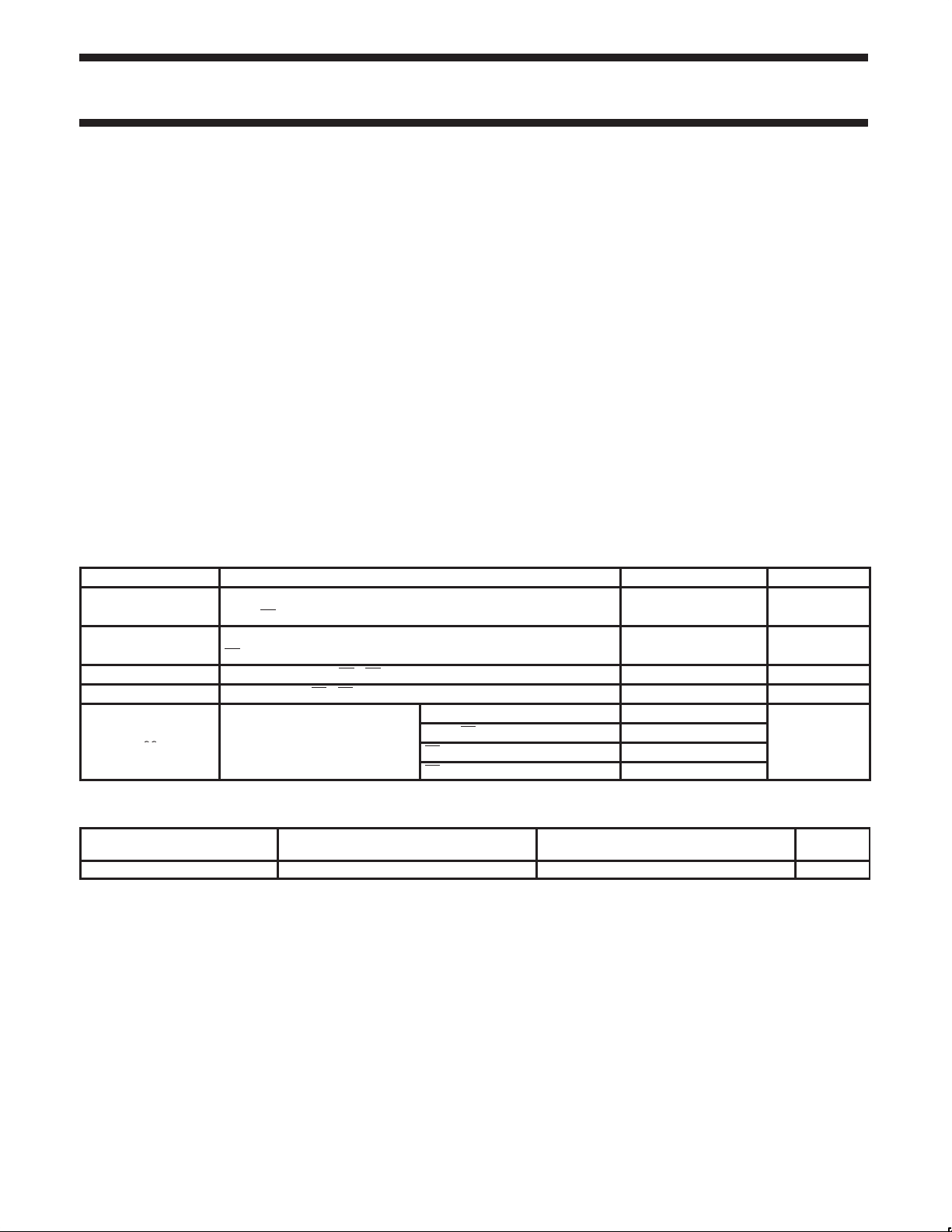
QUICK REFERENCE DATA
SYMBOL PARAMETER TYPICAL UNIT
t
PLH
t
PHL
t
PLH
t
PHL
C
I
OB
OL
CC
Propagation delay 3.7
AIn to Bn 2.7
Propagation delay 3.4
Bn to AOn 3.2
Output capacitance (B0 - B6 only) 6 pF
Output current (B0 - B6 only) 100 mA
Standby 19
pp
AIn to Bn (outputs Low or High) 40
Bn to AOn (outputs Low) 22
Bn to AOn (outputs High) 19
ORDERING INFORMATION
PACKAGE
52-pin Plastic Quad Flatpack FB2041BB CD3207BB SOT379-1
1995 May 25 853-1561 15279
COMMERCIAL RANGE
VCC = 5V±10%; T
= 0 to +70°C
amb
2
INDUSTRIAL RANGE
VCC = 5V±10%; T
= -40 to +85°C
amb
DWG
No.
Philips Semiconductors Product specification
FB20417-bit Futurebus+ transceiver
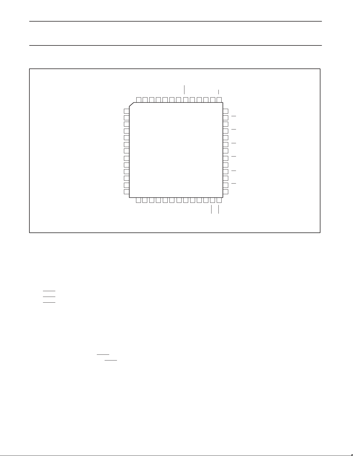
PIN CONFIGURATION
CC
LOGIC V
AI0
AO1
AO0
52 51 50 49 48 47 46 45 44 43 42 41 40
LOGIC GND
LOGIC GND
LOGIC GND
LOGIC GND
LOGIC GND
AI1
AI2
AO2
AO3
AI3
AI4
AO4
AO5
1
2
3
4
5
6
7
8
9
10
11
12
13
14 15 16 17 18 19 20 21 22 23 24 25 26
AI5
7-Bit Transceiver
52-lead PQFP
CC
AO6
LOGIC V
LOGIC GND
The B-port interfaces to “Backplane Transceiver Logic” (See the
IEEE 1194.1 BTL standard). BTL features low power consumption
by reducing voltage swing (1Vp-p, between 1V and 2V) and reduced
capacitive loading by placing an internal series diode on the drivers.
BTL also provides incident wave switching, a necessity for high
performance backplanes.
There are three separate pairs of driver enables in a 1 bit, 3 bit, 3 bit
arrangement. The TTL/BTL output drivers for bit 0 are enabled with
OEA1/OEB1
OEA2/OEB2
OEA3/OEB3
, output drivers for bits 1–2–3 are enabled with
and output drivers for bits 4–5–6 are enabled with
.
The A-port operates at TTL levels with separate I/O. The 3-state
A-port drivers are enabled when OEAn goes High after an extra 6ns
delay which is built in to provide a break-before-make function.
When OEAn goes Low, A-port drivers become High impedance
without any extra delay. During power on/of f cycles, the A-port
drivers are held in a High impedance state when V
is below 2.5V.
CC
The B-port has an output enable, OEB0, which affects all seven
drivers. When OEB0 is High and OEBn
be enabled. When OEB0 is Low or if OEBn
is Low the output driver will
is High, the B-port
drivers will be inactive and at the level of the backplane signal.
CC
B0
TMS (option)
OEB0
OEB1
OEA2
TDO (option)
TCK (option)
BUS V
CC
OEA3
BUS V
TDI (option)
BUS GND
39
38
37
36
35
34
33
32
31
30
29
28
27
OEB2
OEB3
BUS GND
B1
BUS GND
B2
BUS GND
B3
BUS GND
B4
BUS GND
B5
BUS GND
B6
BUS GND
BIAS V
OEA1
FB2041
AI6
LOGIC GND
To support live insertion, OEB0 is held Low during power on/off
cycles to insure glitch free B port drivers. Proper bias for B port
drivers during live insertion is provided by the BIAS V pin when at a
5V level while V
BIAS V pin should be tied to a V
is Low. If live insertion is not a requirement, the
CC
CC
pin.
The LOGIC GND and BUS GND pins are isolated in the package to
minimize noise coupling between the BTL and TTL sides. These
pins should be tied to a common ground external to the package.
Each BTL driver has an associated BUS GND pin that acts as a
signal return path and these BUS GND pins are internally isolated
from each other. In the event of a ground return fault, a “hard” signal
failure occurs instead of a pattern dependent error that may be very
infrequent and impossible to trouble-shoot.
The LOGIC V
and BUS VCC pins are also isolated internally to
CC
minimize noise and may be externally decoupled separately or
simply tied together.
JTAG boundary scan functionality is provided as an option with
signals TMS, TCK, TDI and TDO. When this option is not present,
TMS and TCK are no-connects (no bond wires) and TDI and TDO
are shorted together internally.
1995 May 25
3
Philips Semiconductors Product specification
V
In ut voltage
I
VIHHigh-level in ut voltage
VILLow-level in ut voltage
IOLLow-level out ut current
FB20417-bit Futurebus+ transceiver
PIN DESCRIPTION
SYMBOL PIN NUMBER TYPE NAME AND FUNCTION
AI0 – AI6 51, 2, 3, 8, 9, 14, 18 Input Data inputs (TTL)
AO0 – AO6 50, 52, 4, 6, 10, 12, 16 Output 3-state outputs (TTL)
B0 – B6 40, 38, 36, 34, 32, 30, 28 I/O Data inputs/Open Collector outputs, High current drive (BTL)
OEB0 46 Input Enables the Bn outputs when High
OEB1 45 Input Enables the B0 output when Low
OEB2 25 Input Enables the B1 – B3 outputs when Low
OEB3 26 Input Enables the B4 – B6 outputs when Low
OEA1 47 Input Enables the A0 outputs when High
OEA2 20 Input Enables the A1 – A3 outputs when High
OEA3 24 Input Enables the A4 – A6 outputs when High
BUS GND 41, 39, 37, 35, 33, 31, 29, 27 GND Bus ground (0V)
LOGIC GND 1, 5, 7, 11, 13, 15, 19 GND Logic ground (0V)
BUS V
CC
LOGIC V
CC
BIAS V 48 Power Positive supply voltage
TMS 42 Input Test Mode Select (no-connect)
TCK 44 Input Test Clock (no-connect)
TDI 22 Input Test Data In (shorted to TDO)
TDO 21 Output Test Data Out (TDI)
23, 43 Power Positive supply voltage
17, 49 Power Positive supply voltage
ABSOLUTE MAXIMUM RATINGS
Operation beyond the limits set forth in this table may impair the useful life of the device. Unless otherwise noted these limits are over the
operating free-air temperature range.
SYMBOL
V
CC
IN
I
IN
V
OUT
OUT
T
STG
Supply voltage -0.5 to +7.0 V
p
Input current -18 to +5.0 mA
Voltage applied to output in High output state -0.5 to +V
Current applied to output in AO0 – AO6 48 mA
Low output state B0 – B6 200
Storage temperature -65 to +150 °C
PARAMETER RATING UNIT
AI0 – AI6, OEB0, OEBn, OEAn -1.2 to +7.0 V
B0 – B6 -1.2 to +5.5
CC
RECOMMENDED OPERATING CONDITIONS
SYMBOL
V
CC
I
IK
I
OH
C
OB
T
amb
COMMERCIAL LIMITS
PARAMETER
VCC = 5V±10%;
T
= 0 to +70°C
amb
MIN TYP MAX MIN TYP MAX
Supply voltage 4.5 5.0 5.5 4.5 5.0 5.5 V
p
p
Except B0–B6 2.0 2.0 V
B0 – B6 1.62 1.55 1.62 1.55
Except B0–B6 0.8 0.8 V
B0 – B6 1.47 1.47
Input clamp current -18 -18 mA
High-level output current AO0 – AO6 -3 -3 mA
p
AO0 – AO6 24 24 mA
B0 – B6 100 100
Output capacitance on B port 6 7 6 7 pF
Operating free-air temperature range 0 +70 -40 +85 °C
INDUSTRIAL LIMITS
VCC = 5V±10%;
T
= -40 to +85°C
amb
V
UNIT
1995 May 25
4
Philips Semiconductors Product specification
FB20417-bit Futurebus+ transceiver
FUNCTION TABLE
MODE INPUTS OUTPUTS
AIn Bn* OEB0 OEB1 OEB2 OEB3 OEA1 OEA2 OEA3 AOn Bn*
L — H L L L L L L Z H**
AIn to Bn H — H L L L L L L Z L
L — H L L L H H H L H**
H — H L L L H H H H L
L — H L X X L L L Z H**
AI0 to B0 H — H L X X L L L Z L
L — H L X X H H H L H**
H — H L X X H H H H L
L — H X L X L L L Z H**
AI1 – AI3 to B1 – B3 H — H X L X L L L Z L
L — H X L X H H H L H**
H — H X L X H H H H L
L — H X X L L L L Z H**
AI4 – AI6 to B4 – B6 H — H X X L L L L Z L
L — H X X L H H H L H**
H — H X X L H H H H L
Disable Bn outputs X X L X X X X X X X H**
X X X H H H X X X X H**
Disable B0 outputs X X H H X X X X X X H**
Disable B1 – B3 outputs X X H X H X X X X X H**
Disable B4 – B6 outputs X X H X X H X X X X H**
X L L X X X H H H H Input
Bn to AOn X H L X X X H H H L Input
X L X H H H H H H H Input
X H X H H H H H H L Input
X L L X X X H X X H Input
B0 to AO0 X H L X X X H X X L Input
X L X H H H H X X H Input
X H X H H H H X X L Input
X L L X X X X H X H Input
B1 – B3 to AO1 – AO3 X H L X X X X H X L Input
X L X H H H X H X H Input
X H X H H H X H X L Input
X L L X X X X X H H Input
B4 – B6 to AO4 – AO6 X H L X X X X X H L Input
X L X H H H X X H H Input
X H X H H H X X H L Input
Disable AOn outputs X X X X X X L L L Z X
Disable AO0 outputs X X X X X X L X X Z X
Disable AO1 – AO3 outputs X X X X X X X L X Z X
Disable AO4 – AO6 outputs X X X X X X X X L Z X
NOTES:
H = High voltage level
L = Low voltage level
X = Don’t care
Z = High-impedance (OFF) state
— = Input not externally driven
H** = Goes to level of pull-up voltage
B* = Precaution should be taken to ensure B inputs do not float.
If they do, they are equal to Low state.
Z = High-impedance (OFF) state
— = Input not externally driven
H** = Goes to level of pull-up voltage
B* = Precaution should be taken to ensure B inputs do not float.
If they do, they are equal to Low state.
1995 May 25
5
 Loading...