

Philips BZD142-82, BZD142-68, BZD142-160, BZD142-150, BZD142-130 Datasheet
...
DISCRETE SEMICONDUCTORS
DATA SH EET
ook, halfpage
M3D119
BZD142
ZenBlock
TM
; zener with integrated
blocking diode
Preliminary specification 2000 Dec 19

Philips Semiconductors Preliminary specification
ZenBlockTM; zener with integrated blocking diode
BZD142
FEATURES
• Zener and blocking function in one package
• Glass passivated
• Low leakage current
• Excellent stability
• Available in ammo-pack.
DESCRIPTION
CavityfreecylindricalglasspackagethroughImplotec
TM(1)
MGU216
technology. This package is hermetically sealed and
fatigue free as coefficients of expansion of all used parts
Fig.1 Simplified outline (SOD81) and symbol.
are matched.
(1) Implotec is a trademark of Philips.
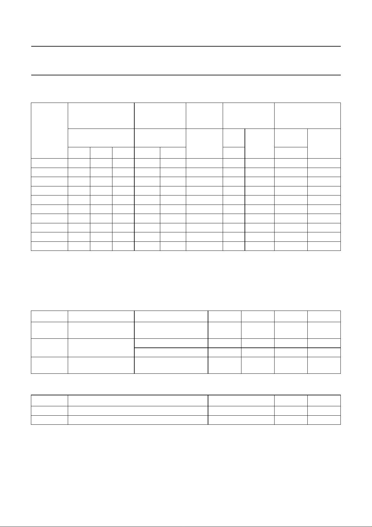
LIMITING VALUES
SYMBOL PARAMETER CONDITIONS MIN. MAX. UNIT
T
stg
T
j
storage temperature −65 +150 °C
junction temperature −65 +150 °C
Zener
P
tot
total power dissipation Ttp=25°C; lead length 10 mm;
− 2.1 W
see Fig.5
Blocking diode
V
E
R
RSM
continuous reverse voltage − 600 V
non-repetitive peak reverse
avalanche energy
L = 120 mH; Tj=T
j(max)
prior to
surge; inductive load switched off
− 10 mJ
2000 Dec 19 2
Philips Semiconductors Preliminary specification
ZenBlockTM; zener with integrated blocking diode
BZD142
ELECTRICAL CHARACTERISTICS ZENER/TVS
Tj=25°C unless otherwise specified.
REVERSE CURRENT
at STAND-OFF
VOLTAGE
IR (µA)
at VR (V)
TYPE
NUMBER
SUFFIX
WORKING VOLTAGE
(1)
VZ(V) at IZ(see Fig.4) SZ(%/K) at I
TEMPERATURE
COEFFICIENT
test
MIN. NOM. MAX. MIN. MAX. MAX. MAX.
TEST
CURRENT
I
(mA)
test
CLAMPING
VOLTAGE
V
(CL)R
(V)
at I
RSM
(A)
(note 2)
68 61 68 75 0.07 0.12 10 94.4 106 5 56
75 68 75 82 0.07 0.12 10 103.5 0.97 5 62
82 74 82 90 0.07 0.12 10 114 0.88 5 68
91 82 91 100 0.07 0.12 5 126 0.79 5 75
100 90 100 110 0.07 0.12 5 139 0.72 5 82
110 99 110 121 0.07 0.12 5 152 0.66 5 91
120 108 120 132 0.07 0.12 5 167 0.60 5 100
130 117 130 143 0.07 0.12 5 185 0.54 5 110
150 135 150 165 0.07 0.12 5 204 0.49 5 120
160 149 160 171 0.07 0.12 5 224 0.45 5 130
Notes
1. To complete the type number the suffix is added to the basic type number, e.g. BZD142-68.
2. Non-repetitive peak reverse current in accordance with
“IEC 60060-1, Section 8”
(10/1000 µs pulse); see Fig.5.
ELECTRICAL CHARACTERISTICS BLOCKING CODE
Tj=25°C unless otherwise specified.
SYMBOL PARAMETER CONDITIONS MIN. TYP. MAX. UNIT
V
(BR)R
reverse avalanche
IR= 0.1 mA 700 −−V
breakdown voltage
I
R
C
d
reverse current VR= 600 V −−5µA
V
= 600 V; Tj= 150 °C −−100 µA
R
diode capacitance f = 1 MHz; VR=0V;
− 15 − pF
see Fig.4
THERMAL CHARACTERISTICS
SYMBOL PARAMETER CONDITIONS VALUE UNIT
R
R
th j-tp
th j-a
thermal resistance from junction to tie-point lead length = 10 mm 60 K/W
thermal resistance from junction to ambient note 1 120 K/W
Note
1. Device mounted on an epoxy-glass printed-circuit board, 1.5 mm thick; thickness of Cu-layer ≥40 µm, see Fig.2.
For more information please refer to the
“General Part of associated Handbook”
.
2000 Dec 19 3
 Loading...