

Philips BZA100 Datasheet

DISCRETE SEMICONDUCTORS
DATA SH EET
M3D184
BZA100
18-fold ESD transient voltage
suppressor
Product specification
Supersedes data of 1996 Mar 21
1997 Dec 02
Philips Semiconductors Product specification
18-fold ESD transient voltage suppressor BZA100
FEATURES
• SO20 SMD package allows 18
separate voltage regulator diodes
in a common anode configuration
• Working voltage: typ. 6.8 V
• Forward voltage: max. 1.3 V
• Maximum reverse peak power
dissipation: 27.5 W at tp=1ms
• Maximum clamping voltage at peak
pulse current: 11 V at 2.5 A
• Low leakage current: max. 2 µA
• ESD rating >8 kV, according
IEC 801-2.
APPLICATIONS
• Where transient overvoltage
protection in voltage and ESD
sensitive equipment is required
such as:
– Computers
– Printers
– Business machines
– Communication systems
– Medical equipment.
DESCRIPTION
18-fold monolitic transient voltage
suppressor. Its 18-fold junction
common anode design protects 18
separate lines using only one
package. This device is ideal for
situations where board space is a
premium.
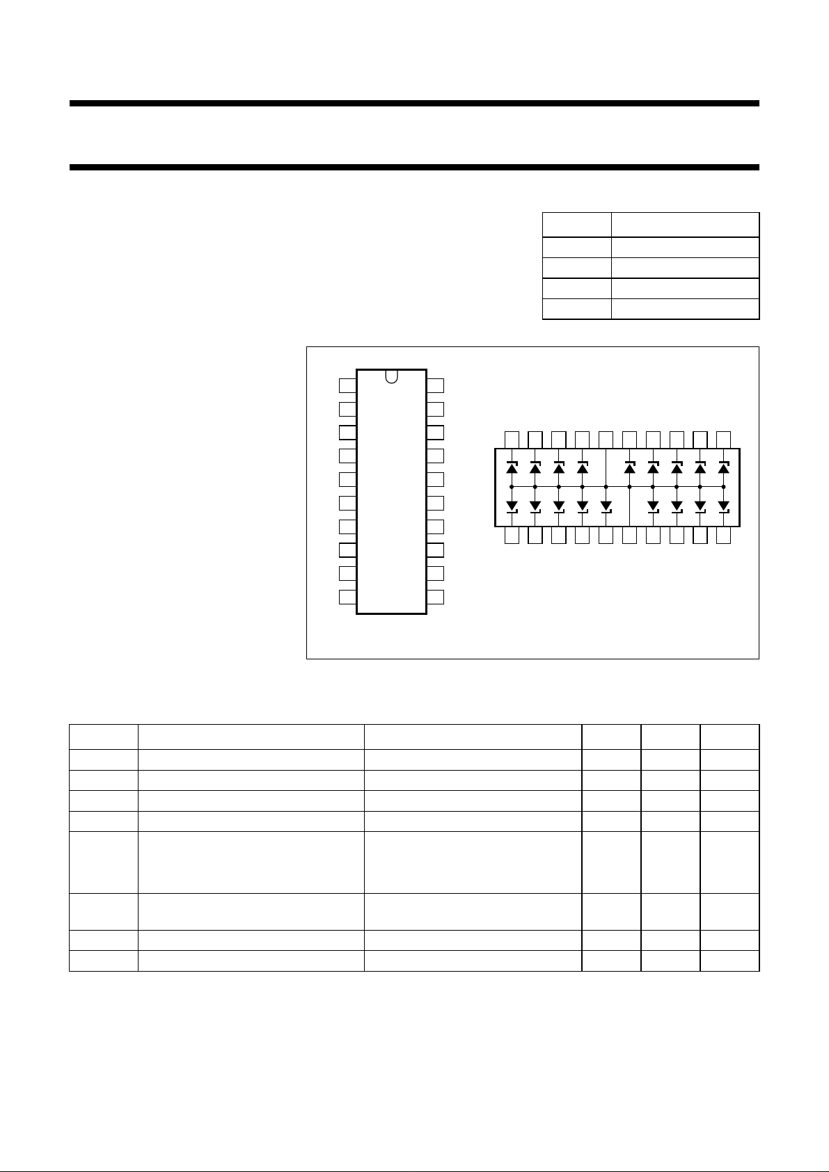
handbook, 4 columns
k
1
1
k
2
2
k
3
3
k
4
4
k
5
5
a
6
1
k
7
6
k
8
7
k
9
8
k
10
9
SO20
k
20
18
k
19
17
k
18
16
k
17
15
a
16
2
k
15
14
k
14
13
k
13
12
k
12
11
k
11
10
Fig.1 Pin configuration for SO20 (SOT163-1) and symbol.
PINNING
PIN DESCRIPTION
1 to 5 cathode (k
6 and 16 common anode (a
7 to 15 cathode (k
17 to 20 cathode (k
19 18 17 16 15 14 13 12 1120
2 3 4 5 6 7 8 9 101
to k5)
1
to k14)
6
to k18)
15
; a2)
1
MBG396
LIMITING VALUES
In accordance with the Absolute Maximum Rating System (IEC 134).
SYMBOL PARAMETER CONDITIONS MIN. MAX. UNIT
I
Z
I
F
I
FSM
I
ZSM
P
tot
P
ZSM
working current − note 1 mA
continuous forward current − 200 mA
non-repetitive peak forward current tp= 1 ms; square pulse − 4A
non-repetitive peak reverse current tp= 1 ms; square pulse; see Fig.2 − 2.5 A
total power dissipation see Fig.3
non-repetitive peak reverse power
up to T
up to T
tp= 1 ms; square pulse; see Fig.4 − 27.5 W
=60°C; note 2 − 1.6 W
s
=25°C; note 3 − 1.25 W
amb
dissipation
T
stg
T
j
storage temperature −65 +150 °C
operating junction temperature − 150 °C
Notes
1. DC working current limited by P
tot max
.
2. One or more diodes loaded; Tsis the temperature at the soldering point.
3. One or more diodes loaded; device mounted on a printed-circuit board with R
= 43.5 K/W.
th a-s
1997 Dec 02 2

Philips Semiconductors Product specification
18-fold ESD transient voltage suppressor BZA100
THERMAL CHARACTERISTICS
SYMBOL PARAMETER CONDITIONS VALUE UNIT
R
th j-s
R
th j-a
ELECTRICAL CHARACTERISTICS
=25°C unless otherwise specified.
T
j
SYMBOL PARAMETER CONDITIONS MIN. TYP. MAX. UNIT
Per diode
V
Z
V
F
V
ZSM
I
R
r
dif
S
Z
C
d
thermal resistance from junction to soldering point one or more diodes loaded 56.5 K/W
thermal resistance from junction to ambient 100 K/W
working voltage IZ = 5 mA 6.4 6.8 7.2 V
forward voltage IF= 200 mA −−1.3 V
non-repetitive peak reverse voltage tp= 1 ms; I
= 2.5 A −−11 V
ZSM
reverse current VR= 5.25 V −−2µA
differential resistance IZ=1mA −−40 Ω
=5mA −−8Ω
I
Z
temperature coefficient of
IZ= 5mA − 3 − mV/K
working voltage
diode capacitance see Fig.5
V
= 0; f = 1 MHz −−120 pF
R
V
= 5.25 V; f = 1 MHz −−60 pF
R
1997 Dec 02 3
 Loading...