

Philips BYW29EX-200 Datasheet
Philips Semiconductors Product specification
Rectifier diodes BYW29EX series
ultrafast, rugged
GENERAL DESCRIPTION QUICK REFERENCE DATA
Glass passivated epitaxial rectifier SYMBOL PARAMETER MAX. MAX. UNIT
diodes in a full pack plastic envelope,
featuring low forward voltage drop, BYW29EX- 150 200
ultra-fast recovery times, soft recovery V
RRM
characteristic and guaranteed reverse voltage
surge and ESD capability. They are V
intendedforuseinswitchedmodepower I
supplies and high frequency circuits in t
general where low conduction and I
switching losses are essential. current
F
F(AV)
rr
RRM
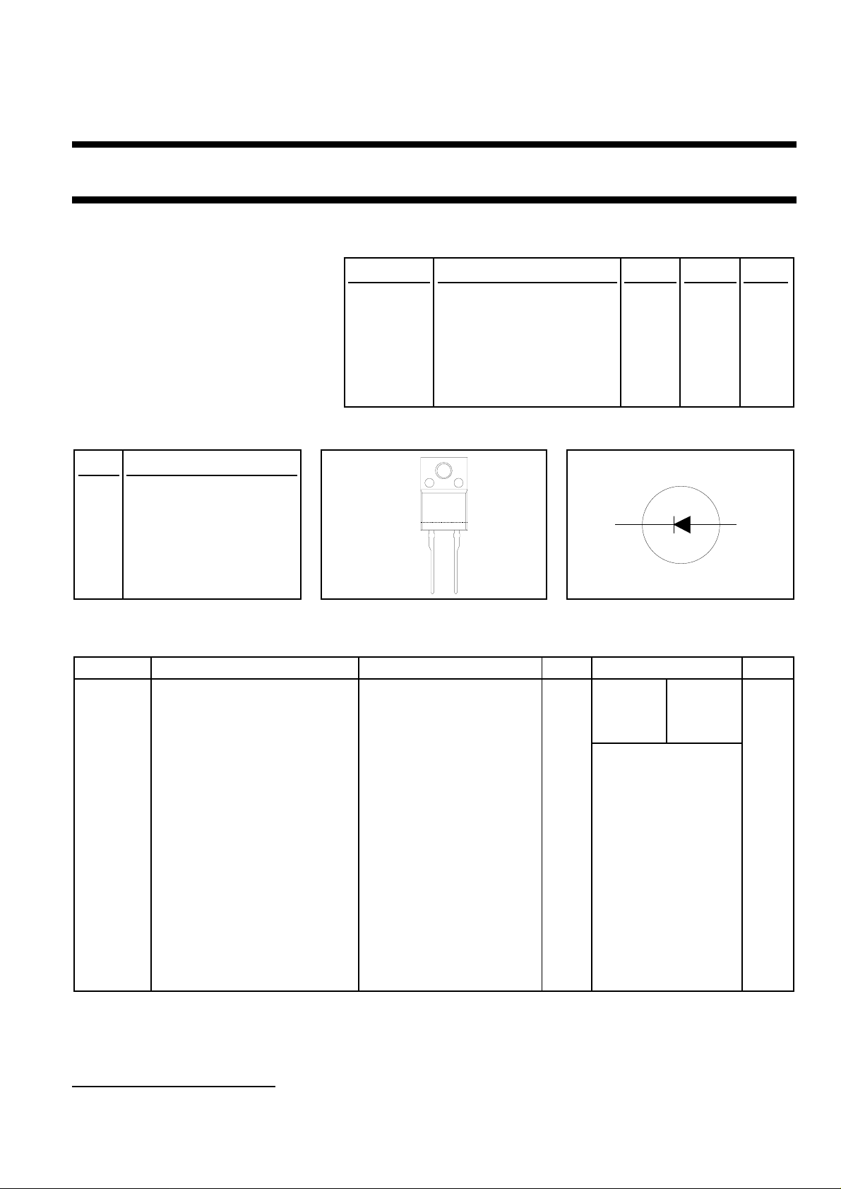
PINNING - SOD113 PIN CONFIGURATION SYMBOL
Repetitive peak reverse 150 200 V
Forward voltage 0.895 0.895 V
Forward current 8 8 A
Reverse recovery time 25 25 ns
Repetitive peak reverse 0.2 0.2 A
PIN DESCRIPTION
case
1 cathode
2 anode
k a
12
case isolated
12
LIMITING VALUES
Limiting values in accordance with the Absolute Maximum System (IEC 134).
SYMBOL PARAMETER CONDITIONS MIN. MAX. UNIT
-150 -200
V
RRM
V
RWM
V
R
I
F(AV)
I
F(RMS)
I
FRM
I
FSM
I2tI
I
RRM
I
RSM
T
stg
T
j
Repetitive peak reverse voltage - 150 200 V
Crest working reverse voltage - 150 200 V
Continuous reverse voltage - 150 200 V
Average forward current
1
square wave; δ = 0.5;
Ths ≤ 106 ˚C - 8 A
sinusoidal; a = 1.57;
Ths ≤ 109 ˚C - 7.3 A
RMS forward current - 11.3 A
Repetitive peak forward current t = 25 µs; δ = 0.5; - 16 A
Ths ≤ 106 ˚C
Non-repetitive peak forward t = 10 ms - 80 A
current t = 8.3 ms - 88 A
sinusoidal; with reapplied
V
2
t for fusing t = 10 ms - 32 A2s
RWM(max)
Repetitive peak reverse current tp = 2 µs; δ = 0.001 - 0.2 A
Non-repetitive peak reverse tp = 100 µs - 0.2 A
current
Storage temperature -40 150 ˚C
Operating junction temperature - 150 ˚C
1 Neglecting switching and reverse current losses
October 1998 1 Rev 1.200

Philips Semiconductors Product specification
Rectifier diodes BYW29EX series
ultrafast, rugged
ESD LIMITING VALUE
SYMBOL PARAMETER CONDITIONS MIN. MAX. UNIT
V
C
Electrostatic discharge Human body model; - 8 kV
capacitor voltage C = 250 pF; R = 1.5 kΩ
ISOLATION LIMITING VALUE & CHARACTERISTIC
Ths = 25 ˚C unless otherwise specified
SYMBOL PARAMETER CONDITIONS MIN. TYP. MAX. UNIT
V
isol
R.M.S. isolation voltage from f = 50-60 Hz; sinusoidal - 2500 V
both terminals to external waveform;
heatsink R.H. ≤ 65% ; clean and dustfree
C
isol
Capacitance from both terminals f = 1 MHz - 10 - pF
to external heatsink
THERMAL RESISTANCES
SYMBOL PARAMETER CONDITIONS MIN. TYP. MAX. UNIT
R
th j-hs
Thermal resistance junction to with heatsink compound - - 5.5 K/W
heatsink without heatsink compound - - 7.2 K/W
R
th j-a
Thermal resistance junction to in free air - 55 - K/W
ambient
STATIC CHARACTERISTICS
Tj = 25 ˚C unless otherwise stated
SYMBOL PARAMETER CONDITIONS MIN. TYP. MAX. UNIT
V
F
I
R
Forward voltage IF = 8 A; Tj = 150˚C - 0.80 0.895 V
IF = 8 A - 0.92 1.05 V
IF = 20 A - 1.1 1.3 V
Reverse current VR = V
VR = V
; Tj = 100 ˚C - 0.2 0.6 mA
RWM
RWM
-210µA
DYNAMIC CHARACTERISTICS
Tj = 25 ˚C unless otherwise stated
SYMBOL PARAMETER CONDITIONS MIN. TYP. MAX. UNIT
Q
s
t
rr1
t
rr2
V
fr
October 1998 2 Rev 1.200
Reverse recovery charge IF = 2 A; VR ≥ 30 V; -dIF/dt = 20 A/µs- 4 11 nC
Reverse recovery time IF = 1 A; VR ≥ 30 V; - 20 25 ns
-dIF/dt = 100 A/µs
Reverse recovery time IF = 0.5 A to IR = 1 A; I
Forward recovery voltage IF = 1 A; dIF/dt = 10 A/µs-1-V
= 0.25 A - 15 20 ns
rec
 Loading...