

Philips BYW29EB-150, BYW29ED-150 Datasheet

Philips Semiconductors Product specification
Rectifier diodes BYW29EB, BYW29ED series
ultrafast, rugged
FEATURES SYMBOL QUICK REFERENCE DATA
• Low forward volt drop VR = 150 V/ 200 V
• Fast switching
• Soft recovery characteristic VF ≤ 0.895 V
• Reverse surge capability
• High thermal cycling performance I
• Low thermal resistance
GENERAL DESCRIPTION
Ultra-fast,epitaxialrectifierdiodes intendedfor useasoutputrectifiers inhighfrequencyswitchedmode powersupplies.
The BYW29EB series is supplied in the SOT404 surface mounting package.
The BYW29ED series is supplied in the SOT428 surface mounting package.
PINNING SOT404 SOT428
k a
tab 3
= 8 A
F(AV)
I
= 0.2 A
RRM
trr ≤ 25 ns
PIN DESCRIPTION
tab
tab
1 no connection
2 cathode
3 anode
tab cathode
1
2
13
123
LIMITING VALUES
Limiting values in accordance with the Absolute Maximum System (IEC 134)
SYMBOL PARAMETER CONDITIONS MIN. MAX. UNIT
BYW29EB/ BYW29ED -150 -200
V
RRM
V
RWM
V
R
I
F(AV)
I
FRM
I
FSM
I
RRM
I
RSM
T
j
T
stg
1. It is not possible to make connection to pin 2 of the SOT428 or SOT404 packages.
Peak repetitive reverse - 150 200 V
voltage
Working peak reverse - 150 200 V
voltage
Continuous reverse voltage - 150 200 V
Average rectified forward square wave; δ = 0.5; Tmb ≤ 128 ˚C - 8 A
current
Repetitive peak forward square wave; δ = 0.5; Tmb ≤ 128 ˚C - 16 A
current
Non-repetitive peak forward t = 10 ms - 80 A
current t = 8.3 ms - 88 A
sinusoidal; with reapplied V
RRM(max)
Peak repetitive reverse tp = 2 µs; δ = 0.001 - 0.2 A
surge current
Peak non-repetitive reverse tp = 100 µs - 0.2 A
surge current
Operating junction - 150 ˚C
temperature
Storage temperature - 40 150 ˚C
November 1998 1 Rev 1.300

Philips Semiconductors Product specification
Rectifier diodes BYW29EB, BYW29ED series
ultrafast, rugged
ESD LIMITING VALUE
SYMBOL PARAMETER CONDITIONS MIN. MAX. UNIT
V
C
Electrostatic discharge Human body model; - 8 kV
capacitor voltage C = 250 pF; R = 1.5 kΩ
THERMAL RESISTANCES
SYMBOL PARAMETER CONDITIONS MIN. TYP. MAX. UNIT
R
R
th j-mb
th j-a
Thermal resistance junction - - 2.7 K/W
to mounting base
Thermal resistance junction SOT404 and SOT428 packages, pcb - 50 - K/W
to ambient mounted, minimum footprint, FR4 board
ELECTRICAL CHARACTERISTICS
Tj = 25 ˚C unless otherwise specified
SYMBOL PARAMETER CONDITIONS MIN. TYP. MAX. UNIT
V
F
I
R
Q
rr
t
rr1
t
rr2
V
fr
Forward voltage IF = 8 A; Tj = 150˚C - 0.8 0.895 V
IF = 8 A - 0.92 1.05 V
IF = 20 A - 1.1 1.3 V
Reverse current VR = V
Reverse recovered charge IF = 2 A; VR ≥ 30 V; -dIF/dt = 20 A/µs-411nC
VR = V
RWM
; Tj = 100˚C - 0.2 0.6 mA
RWM
-210µA
Reverse recovery time IF = 1 A; VR ≥ 30 V; -dIF/dt = 100 A/µs2025ns
Reverse recovery time IF = 0.5 A to IR = 1 A; I
Forward recovery voltage IF = 1 A; dIF/dt = 10 A/µs-1-V
= 0.25 A - 15 20 ns
rec
November 1998 2 Rev 1.300
Philips Semiconductors Product specification
Rectifier diodes BYW29EB, BYW29ED series
ultrafast, rugged
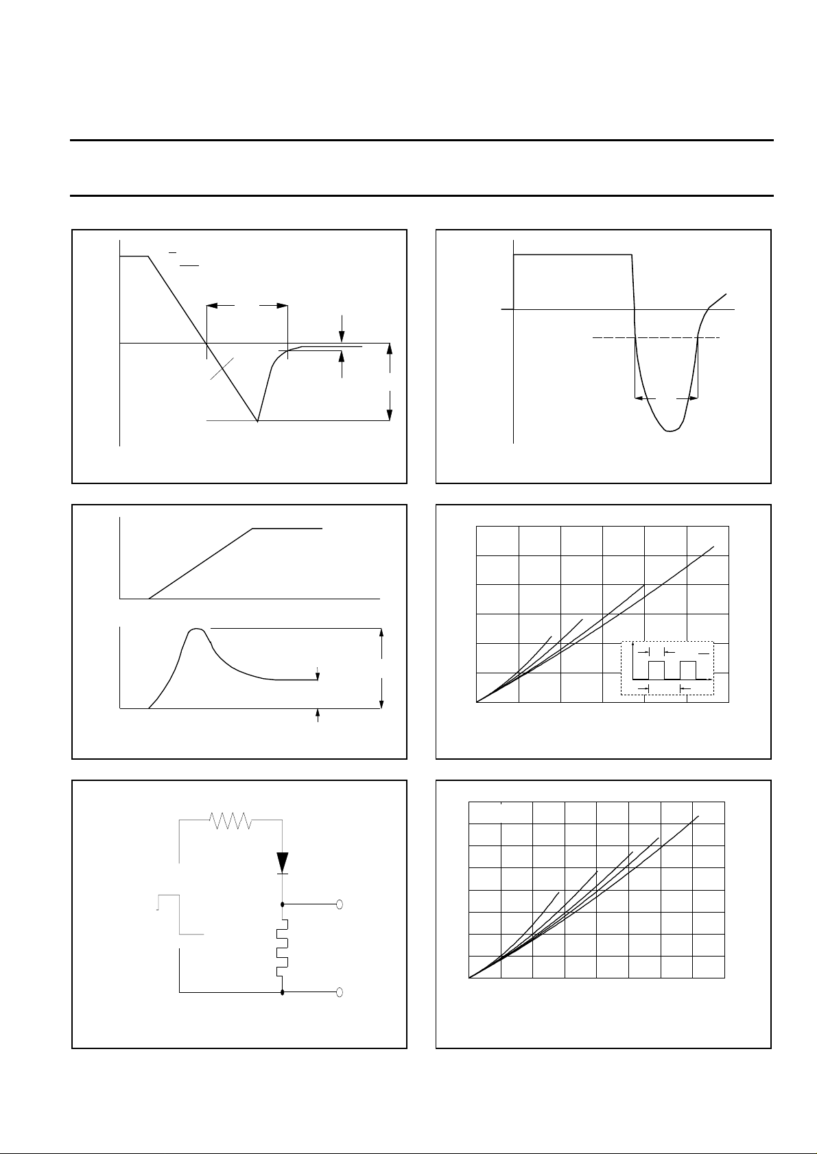
I
F
dI
F
dt
t
rr
time
Q
s
I
R
I
F
I
rrm
Fig.1. Definition of t
, Qs and I
rr1
10%
rrm
100%
time
V
F
V
fr
V
F
time
Fig.2. Definition of V
fr
0.5A
IF
0A
I = 0.25A
rec
IR
trr2
I = 1A
R
Fig.4. Definition of t
PF / W
12
Vo = 0.791 V
Rs = 0.013 Ohms
10
8
6
4
2
0
024681012
0.1
BYW29
0.2
IF(AV) / A
rr2
Tmb(max) / C
D = 1.0
0.5
p
p
t
I
t
D =
T
T
t
Fig.5. Maximum forward dissipation PF = f(I
square current waveform where I
F(AV)
=I
F(RMS)
108
115
122
129
136
143
150
);
F(AV)
x √D.
2.2
F(AV)
Tmb(max) / C
a = 1.57
1.9
.
122
125.5
129
132.5
136
139.5
143
146.5
150
F(AV)
);
R
Voltage Pulse Source
Current
shunt
Fig.3. Circuit schematic for t
D.U.T.
to ’scope
rr2
PF / W
8
Vo = 0.791 V
Rs = 0.013 Ohms
7
6
5
4
3
2
1
0
012345678
BYW29
2.8
4
IF(AV) / A
Fig.6. Maximum forward dissipation PF = f(I
sinusoidal current waveform where a = form
factor = I
F(RMS)
/ I
November 1998 3 Rev 1.300
 Loading...