

Philips BYW29EB-200, BYW29EB-100, BYW29ED-200, BYW29ED-100 Datasheet
Philips Semiconductors Product specification
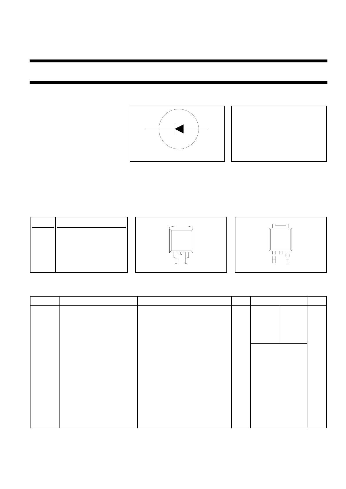
Rectifier diodes BYW29EB, BYW29ED series
ultrafast, rugged
FEATURES SYMBOL QUICK REFERENCE DATA
• Low forward volt drop VR = 150 V/ 200 V
• Fast switching
• Soft recovery characteristic VF ≤ 0.895 V
• Reverse surge capability
• High thermal cycling performance I
F(AV)
= 8 A
• Low thermal resistance
I
RRM
= 0.2 A
trr ≤ 25 ns
GENERAL DESCRIPTION
Ultra-fast,epitaxialrectifierdiodes intendedfor useasoutputrectifiers inhighfrequencyswitchedmode powersupplies.
The BYW29EB series is supplied in the SOT404 surface mounting package.
The BYW29ED series is supplied in the SOT428 surface mounting package.
PINNING SOT404 SOT428
PIN DESCRIPTION
1 no connection
2 cathode
1
3 anode
tab cathode
LIMITING VALUES
Limiting values in accordance with the Absolute Maximum System (IEC 134)
SYMBOL PARAMETER CONDITIONS MIN. MAX. UNIT
BYW29EB/ BYW29ED -150 -200
V
RRM
Peak repetitive reverse - 150 200 V
voltage
V
RWM
Working peak reverse - 150 200 V
voltage
V
R
Continuous reverse voltage - 150 200 V
I
F(AV)
Average rectified forward square wave; δ = 0.5; Tmb ≤ 128 ˚C - 8 A
current
I
FRM
Repetitive peak forward square wave; δ = 0.5; Tmb ≤ 128 ˚C - 16 A
current
I
FSM
Non-repetitive peak forward t = 10 ms - 80 A
current t = 8.3 ms - 88 A
sinusoidal; with reapplied V
RRM(max)
I
RRM
Peak repetitive reverse tp = 2 µs; δ = 0.001 - 0.2 A
surge current
I
RSM
Peak non-repetitive reverse tp = 100 µs - 0.2 A
surge current
T
j
Operating junction - 150 ˚C
temperature
T
stg
Storage temperature - 40 150 ˚C
1. It is not possible to make connection to pin 2 of the SOT428 or SOT404 packages.
k a
tab 3
123
tab
13
tab
2
November 1998 1 Rev 1.300

Philips Semiconductors Product specification
Rectifier diodes BYW29EB, BYW29ED series
ultrafast, rugged
ESD LIMITING VALUE
SYMBOL PARAMETER CONDITIONS MIN. MAX. UNIT
V
C
Electrostatic discharge Human body model; - 8 kV
capacitor voltage C = 250 pF; R = 1.5 kΩ
THERMAL RESISTANCES
SYMBOL PARAMETER CONDITIONS MIN. TYP. MAX. UNIT
R
th j-mb
Thermal resistance junction - - 2.7 K/W
to mounting base
R
th j-a
Thermal resistance junction SOT404 and SOT428 packages, pcb - 50 - K/W
to ambient mounted, minimum footprint, FR4 board
ELECTRICAL CHARACTERISTICS
Tj = 25 ˚C unless otherwise specified
SYMBOL PARAMETER CONDITIONS MIN. TYP. MAX. UNIT
V
F
Forward voltage IF = 8 A; Tj = 150˚C - 0.8 0.895 V
IF = 8 A - 0.92 1.05 V
IF = 20 A - 1.1 1.3 V
I
R
Reverse current VR = V
RWM
-210µA
VR = V
RWM
; Tj = 100˚C - 0.2 0.6 mA
Q
rr
Reverse recovered charge IF = 2 A; VR ≥ 30 V; -dIF/dt = 20 A/µs-411nC
t
rr1
Reverse recovery time IF = 1 A; VR ≥ 30 V; -dIF/dt = 100 A/µs2025ns
t
rr2
Reverse recovery time IF = 0.5 A to IR = 1 A; I
rec
= 0.25 A - 15 20 ns
V
fr
Forward recovery voltage IF = 1 A; dIF/dt = 10 A/µs-1-V
November 1998 2 Rev 1.300
Philips Semiconductors Product specification
Rectifier diodes BYW29EB, BYW29ED series
ultrafast, rugged
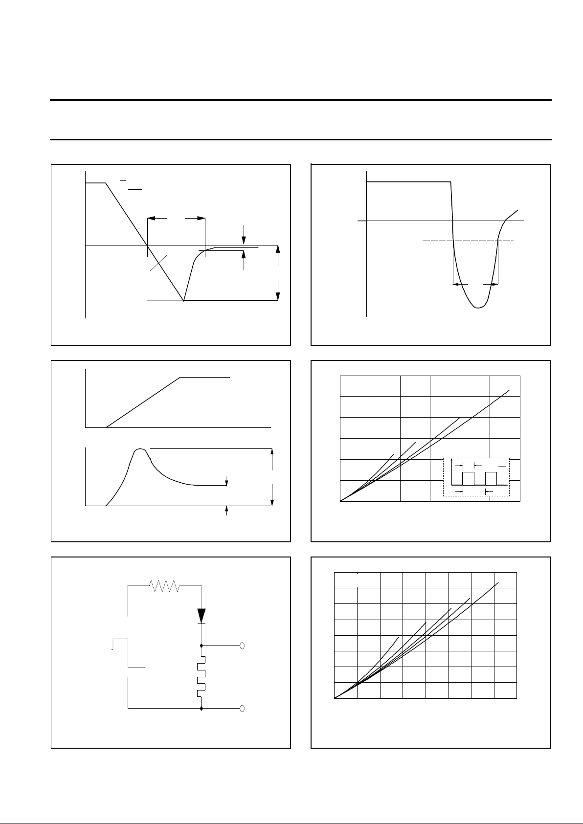
Fig.1. Definition of t
rr1
, Qs and I
rrm
Fig.2. Definition of V
fr
Fig.3. Circuit schematic for t
rr2
Fig.4. Definition of t
rr2
Fig.5. Maximum forward dissipation PF = f(I
F(AV)
);
square current waveform where I
F(AV)
=I
F(RMS)
x √D.
Fig.6. Maximum forward dissipation PF = f(I
F(AV)
);
sinusoidal current waveform where a = form
factor = I
F(RMS)
/ I
F(AV)
.
Q
s
100%
10%
time
dI
dt
F
I
R
I
F
I
rrm
t
rr
I = 1A
R
rec
I = 0.25A
0A
trr2
0.5A
IF
IR
time
time
V
F
V
fr
V
F
I
F
024681012
0
2
4
6
8
10
12
D = 1.0
0.5
0.2
0.1
BYW29
IF(AV) / A
PF / W
D =
t
p
t
p
T
T
t
I
Tmb(max) / C
150
143
136
129
122
115
108
Vo = 0.791 V
Rs = 0.013 Ohms
shunt
Current
to ’scope
D.U.T.
Voltage Pulse Source
R
012345678
0
1
2
3
4
5
6
7
8
a = 1.57
1.9
2.2
2.8
4
BYW29
IF(AV) / A
PF / W
Tmb(max) / C
150
146.5
143
139.5
136
132.5
129
125.5
122
Vo = 0.791 V
Rs = 0.013 Ohms
November 1998 3 Rev 1.300
 Loading...