

Philips BYV29X DATASHEETS

Philips Semiconductors Product specification
Rectifier diodes BYV29F, BYV29X series
ultrafast
FEATURES SYMBOL QUICK REFERENCE DATA
• Low forward volt drop V
= 300 V/ 400 V/ 500 V
R
• Fast switching
• Soft recovery characteristic V
• High thermal cycling performance
• Isolated mounting tab I
k a
12
≤ 1.03 V
F
= 9 A
F(AV)
trr ≤ 60 ns
GENERAL DESCRIPTION
Ultra-fast epitaxial rectifier diodes intended for use in switched mode power supply output rectification, electronic
lighting ballasts and high frequency switching circuits in general.
The BYV29F series is supplied in the SOD100 package.
The BYV29X series is supplied in the SOD113 package.
PINNING SOD100 SOD113
PIN DESCRIPTION
1 cathode (k)
2 anode (a)
tab isolated
case
12
case
12
LIMITING VALUES
Limiting values in accordance with the Absolute Maximum System (IEC 134).
SYMBOL PARAMETER CONDITIONS MIN. MAX. UNIT
BYV29F/BYV29X -300 -400 -500
V
RRM
V
R
I
F(AV)
I
FSM
T
stg
T
j
1 Ths de-rating for thermal stability.
2 Neglecting switching and reverse current losses
Peak repetitive reverse voltage - 300 400 500 V
Continuous reverse voltage Ths ≤ 138˚C
Average forward current
2
square wave; δ = 0.5; - 9 A
1
- 300 400 500 V
Ths ≤ 90 ˚C
Non-repetitive peak forward t = 10 ms - 100 A
current t = 8.3 ms - 110 A
sinusoidal; with reapplied
V
RRM(max)
Storage temperature -40 150 ˚C
Operating junction temperature - 150 ˚C
February 1999 1 Rev 1.400

Philips Semiconductors Product specification
Rectifier diodes BYV29F, BYV29X series
ultrafast
ISOLATION LIMITING VALUE & CHARACTERISTIC
Ths = 25 ˚C unless otherwise specified
SYMBOL PARAMETER CONDITIONS MIN. TYP. MAX. UNIT
V
isol
V
isol
C
isol
THERMAL RESISTANCES
SYMBOL PARAMETER CONDITIONS MIN. TYP. MAX. UNIT
R
th j-hs
R
th j-a
Peak isolation voltage from SOD100 package; R.H. ≤ 65%; clean and - - 1500 V
all terminals to external dustfree
heatsink
R.M.S. isolation voltage from SOD113 package; f = 50-60 Hz; - - 2500 V
all terminals to external sinusoidal waveform; R.H. ≤ 65%; clean
heatsink and dustfree
Capacitance from pin 2 to f = 1 MHz - 10 - pF
external heatsink
Thermal resistance junction to with heatsink compound - - 5.5 K/W
heatsink without heatsink compound - - 7.2 K/W
Thermal resistance junction to in free air. - 55 - K/W
ambient
ELECTRICAL CHARACTERISTICS
Tj = 25 ˚C unless otherwise stated
SYMBOL PARAMETER CONDITIONS MIN. TYP. MAX. UNIT
V
F
I
R
Q
s
t
rr
I
rrm
V
fr
Forward voltage IF = 8 A; Tj = 150˚C - 0.90 1.03 V
IF = 8 A - 1.05 1.25 V
IF = 20 A - 1.20 1.40 V
Reverse current VR = V
Reverse recovery charge IF = 2 A to VR ≥ 30 V; - 40 60 nC
VR = V
RRM
; Tj = 100 ˚C - 0.1 0.35 mA
RRM
- 2.0 50 µA
dIF/dt = 20 A/µs
Reverse recovery time IF = 1 A to VR ≥ 30 V; - 50 60 ns
dIF/dt = 100 A/µs
Peak reverse recovery current IF = 10 A to VR ≥ 30 V; - 4.0 5.5 A
dIF/dt = 50 A/µs; Tj = 100˚C
Forward recovery voltage IF = 10 A; dIF/dt = 10 A/µs - 2.5 - V
February 1999 2 Rev 1.400
Philips Semiconductors Product specification
Rectifier diodes BYV29F, BYV29X series
ultrafast
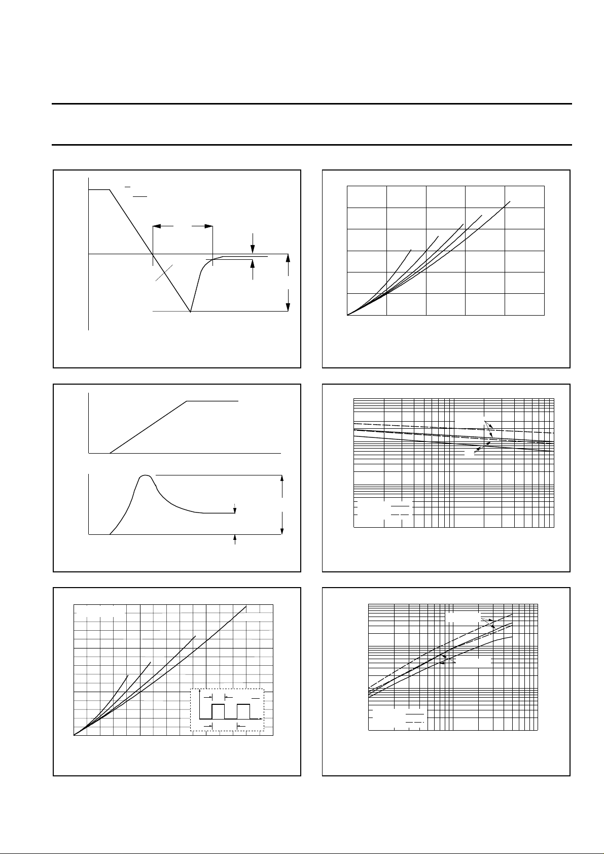
4
BYV29
2.8
IF(AV) / A
F(RMS)
2.2
/ I
IF=10 A
1A
I
F
dI
F
dt
t
rr
time
Q
s
I
R
I
rrm
10%
Fig.1. Definition of trr, Qs and I
100%
rrm
PF / W
12
Vo = 0.89V
Rs = 0.019 Ohms
10
8
6
4
2
0
0246810
Fig.4. Maximum forward dissipation PF = f(I
sinusoidal current waveform where a = form
factor = I
I
F
time
1000
100
trr / ns
F(AV)
Ths(max) / C
1.9
.
a = 1.57
F(AV)
84
95
106
117
128
139
150
);
V
F
V
F
Fig.2. Definition of V
PF / W
15
Vo = 0.8900 V
Rs = 0.0190 Ohms
10
0.1
5
0
0 5 10 15
BYV29
0.5
0.2
IF(AV) / A
fr
Ths(max) / C
D = 1.0
t
p
I
D =
T
Fig.3. Maximum forward dissipation PF = f(I
square wave where I
F(AV)
=I
F(RMS)
x √D.
time
t
p
T
t
67.5
95
122.5
150
F(AV)
10
V
fr
Tj = 25 C
Tj = 100C
1
110
dIF/dt (A/us)
100
Fig.5. Maximum trr at Tj = 25˚C and 100˚C
Irrm / A
10
IF=10A
1
IF=1A
0.1
Tj = 25 C
Tj = 100C
0.01
1
);
Fig.6. Maximum I
10 100
-dIF/dt (A/us)
at Tj = 25˚C and 100˚C.
rrm
February 1999 3 Rev 1.400
 Loading...