

Philips byv143f x DATASHEETS
Philips Semiconductors Product specification
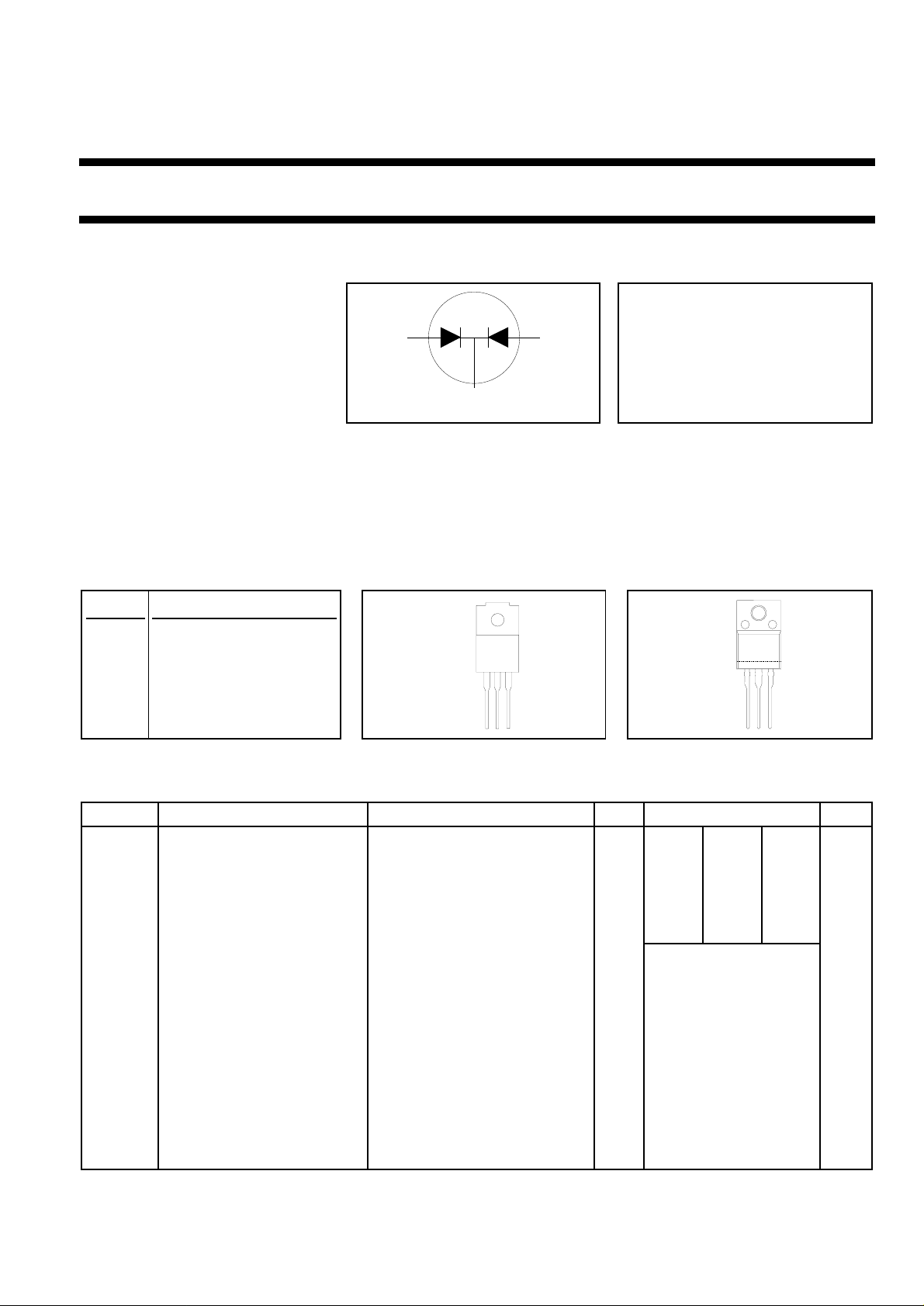
Rectifier diodes BYV143F, BYV143X series
Schottky barrier
FEATURES SYMBOL QUICK REFERENCE DATA
• Low forward volt drop
• Fast switching V
• Reverse surge capability
• High thermal cycling performance I
a1
13
a2
• Isolated package
k
2
GENERAL DESCRIPTION
Dual, common cathode schottky rectifier diodes in a plastic envelope with electrically isolated mounting tab. Intended
for use as output rectifiers in low voltage, high frequency switched mode power supplies.
The BYV143F series is supplied in the SOT186 package.
The BYV143X series is supplied in the SOT186A package.
PINNING SOT186 SOT186A
= 35 V/ 40 V/ 45 V
R
= 20 A
O(AV)
VF ≤ 0.6 V
PIN DESCRIPTION
case
case
1 anode 1 (a)
2 cathode (k)
3 anode 2 (a)
tab isolated
123
123
LIMITING VALUES
Limiting values in accordance with the Absolute Maximum System (IEC 134)
SYMBOL PARAMETER CONDITIONS MIN. MAX. UNIT
BYV143F- 35 40 45
BYV143X- 35 40 45
V
V
V
I
O(AV)
I
FRM
I
FSM
I
RRM
T
T
RRM
RWM
R
j
stg
Peak repetitive reverse - 35 40 45 V
voltage
Working peak reverse - 35 40 45 V
voltage
Continuous reverse voltage Ths ≤ 82 ˚C - 35 40 45 V
Average rectified output square wave; δ = 0.5; - 20 A
current (both diodes Ths ≤ 83 ˚C
conducting)
Repetitive peak forward square wave; δ = 0.5; - 20 A
current per diode Ths ≤ 83 ˚C
Non-repetitive peak forward t = 10 ms - 100 A
current per diode t = 8.3 ms - 110 A
sinusoidal; Tj = 125 ˚C prior to
Peak repetitive reverse pulse width and repetition rate - 1 A
surge; with reapplied V
surge current per diode limited by T
j max
RRM(max)
Operating junction - 150 ˚C
temperature
Storage temperature - 65 175 ˚C
June 1998 1 Rev 1.100
Philips Semiconductors Product specification
Rectifier diodes BYV143F, BYV143X series
Schottky barrier
ISOLATION LIMITING VALUE & CHARACTERISTIC
Ths = 25 ˚C unless otherwise specified
SYMBOL PARAMETER CONDITIONS MIN. TYP. MAX. UNIT
V
isol
V
isol
C
isol
THERMAL RESISTANCES
SYMBOL PARAMETER CONDITIONS MIN. TYP. MAX. UNIT
R
th j-hs
R
th j-a
Peak isolation voltage from SOT186 package; R.H. ≤ 65%; clean and - - 1500 V
all terminals to external dustfree
heatsink
R.M.S. isolation voltage from SOT186A package; f = 50-60 Hz; - - 2500 V
all terminals to external sinusoidal waveform; R.H. ≤ 65%; clean
heatsink and dustfree
Capacitance from pin 2 to f = 1 MHz - 10 - pF
external heatsink
Thermal resistance junction per diode - - 5.7 K/W
to heatsink both diodes - - 4.8 K/W
(with heatsink compound)
Thermal resistance junction in free air - 55 - K/W
to ambient
ELECTRICAL CHARACTERISTICS
Tj = 25 ˚C unless otherwise specified
SYMBOL PARAMETER CONDITIONS MIN. TYP. MAX. UNIT
V
F
I
R
C
d
Forward voltage IF = 15 A; Tj = 125˚C - 0.55 0.62 V
IF = 20 A - 0.65 0.8 V
Reverse current VR = V
VR = V
RWM
; Tj = 100˚C - 15 30 mA
RWM
- 0.12 1.5 mA
Junction capacitance VR = 5 V; f = 1 MHz, Tj = 25˚C to 125˚C - 450 - pF
June 1998 2 Rev 1.100
 Loading...