

Philips BYV118-40, BYV118-35, BYV118B-45, BYV118B-35, BYV118-45 Datasheet
Philips Semiconductors Product specification
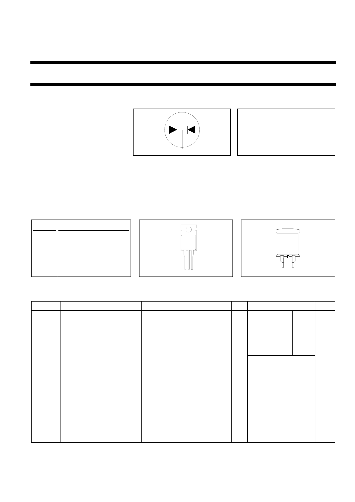
Rectifier diodes BYV118, BYV118B series
Schottky barrier
FEATURES SYMBOL QUICK REFERENCE DATA
• Low forward volt drop V
• Fast switching
• Reverse surge capability I
• High thermal cycling performance
a1
13
a2
• Low thermal resistance V
k
2
= 35 V/ 40 V/ 45 V
R
= 10 A
O(AV)
≤ 0.6 V
F
GENERAL DESCRIPTION
Dual, common cathode schottky rectifier diodes in a conventional leaded plastic package and a surface mounting
plastic package. Intended for use as output rectifiers in low voltage, high frequency switched mode power supplies.
The BYV118 series is supplied in the SOT78 conventional leaded package.
The BYV118B series is supplied in the SOT404 surface mounting package.
PINNING SOT78 (TO220AB) SOT404
PIN DESCRIPTION
1 anode 1 (a)
2 cathode (k)
1
3 anode 2 (a)
tab cathode (k)
tab
123
tab
2
13
LIMITING VALUES
Limiting values in accordance with the Absolute Maximum System (IEC 134)
SYMBOL PARAMETER CONDITIONS MIN. MAX. UNIT
BYV118- 35 40 45
BYV118B- 35 40 45
V
RRM
V
RWM
V
R
I
O(AV)
I
FRM
I
FSM
I
RRM
T
j
T
stg
1. It is not possible to make connection to pin 2 of the SOT404 pckage.
Peak repetitive reverse - 35 40 45 V
voltage
Working peak reverse - 35 40 45 V
voltage
Continuous reverse voltage Tmb ≤ 108 ˚C - 35 40 45 V
Average rectified forward square wave; δ = 0.5; - 10 A
current (both diodes Tmb ≤ 127 ˚C
conducting)
Repetitive peak forward square wave; δ = 0.5; - 10 A
current (per diode) Tmb ≤ 127 ˚C
Non-repetitive peak forward t = 10 ms - 100 A
current per diode t = 8.3 ms - 110 A
sinusoidal; Tj = 125 ˚C prior to
Peak repetitive reverse pulse width and repetition rate - 1 A
surge; with reapplied V
surge current per diode limited by T
j max
RRM(max)
Operating junction - 150 ˚C
temperature
Storage temperature - 65 175 ˚C
May 1998 1 Rev 1.300

Philips Semiconductors Product specification
Rectifier diodes BYV118, BYV118B series
Schottky barrier
THERMAL RESISTANCES
SYMBOL PARAMETER CONDITIONS MIN. TYP. MAX. UNIT
R
th j-mb
R
th j-a
ELECTRICAL CHARACTERISTICS
Tj = 25 ˚C unless otherwise specified
SYMBOL PARAMETER CONDITIONS MIN. TYP. MAX. UNIT
V
F
I
R
C
d
Thermal resistance junction per diode - - 4.5 K/W
to mounting base both diodes - - 3 K/W
Thermal resistance junction SOT78 package in free air - 60 - K/W
to ambient SOT404 package, pcb mounted, minimum - 50 - K/W
footprint, FR4 board
Forward voltage per diode IF = 5 A; Tj = 125˚C - 0.52 0.6 V
IF = 10 A - 0.72 0.87 V
Reverse current per diode VR = V
Junction capacitance per VR = 5 V; f = 1 MHz, Tj = 25˚C to 125˚C - 155 - pF
VR = V
RWM
; Tj = 100˚C - 6 15 mA
RWM
- 0.06 0.5 mA
diode
May 1998 2 Rev 1.300
 Loading...