

Philips by329x DATASHEETS
Philips Semiconductors Product specification
Rectifier diodes BY329X series
fast, soft-recovery
GENERAL DESCRIPTION QUICK REFERENCE DATA
Glass-passivated double diffused SYMBOL PARAMETER MAX. MAX. MAX. UNIT
rectifier diodes in a full pack plastic
envelope featuring low forward BY329X -800 -1000 -1200
voltage drop, fast reverse recovery V
RRM
and soft recovery characteristic. The voltage
devices are intended for use in TV I
receivers, monitors and switched I
F(AV)
FSM
mode power supplies. forward current
t
rr
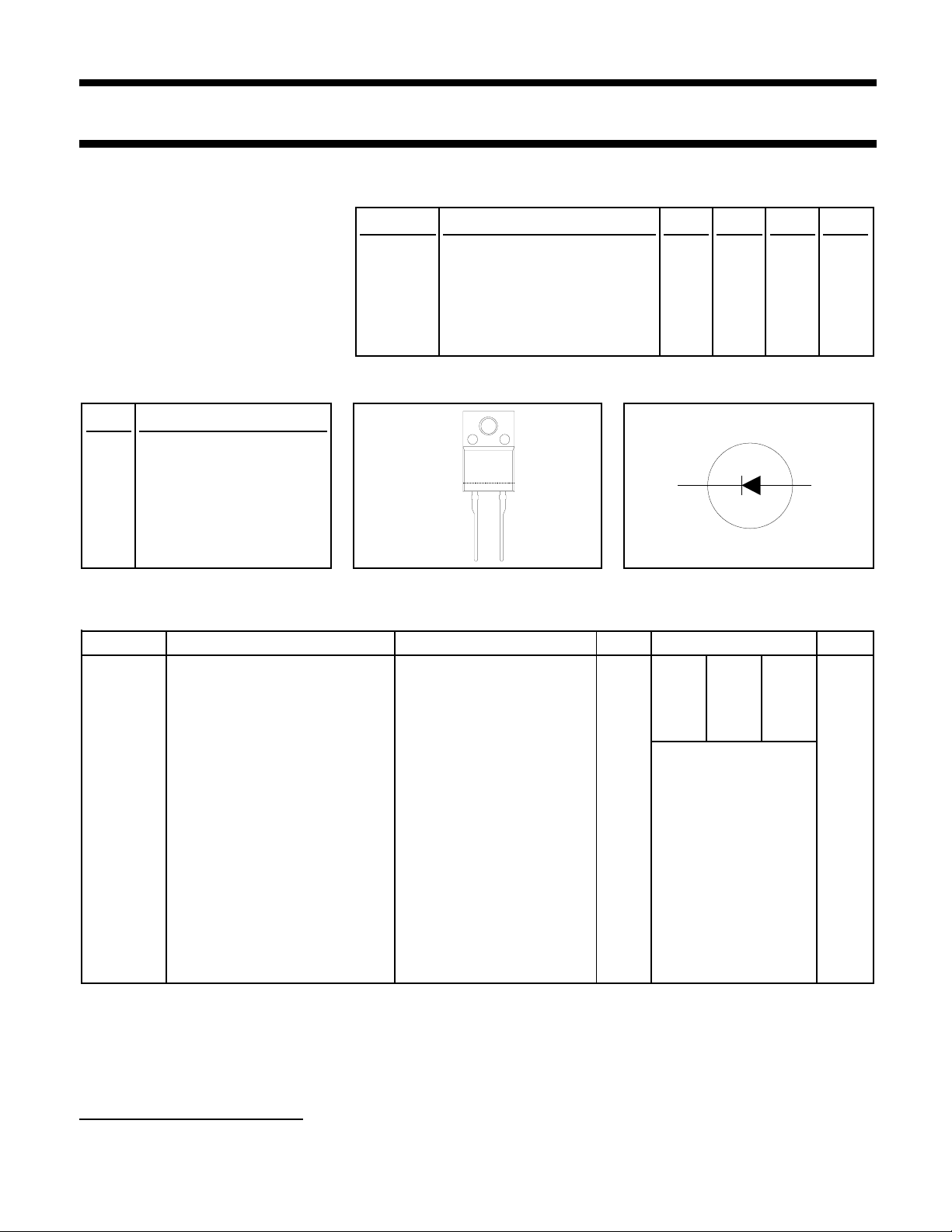
PINNING - SOD113 PIN CONFIGURATION SYMBOL
Repetitive peak reverse 800 1000 1200 V
Average forward current 8 8 8 A
Non-repetitive peak 65 65 65 A
Reverse recovery time 145 145 145 ns
PIN DESCRIPTION
case
1 cathode
2 anode
k a
1
2
case isolated
12
LIMITING VALUES
Limiting values in accordance with the Absolute Maximum System (IEC 134).
SYMBOL PARAMETER CONDITIONS MIN. MAX. UNIT
V
RSM
V
RRM
V
RWM
I
F(AV)
I
F(RMS)
I
FRM
I
FSM
Non-repetitive peak reverse - 800 1000 1200 V
voltage
Repetitive peak reverse voltage - 800 1000 1200 V
Crest working reverse voltage - 600 800 1000 V
Average forward current
RMS forward current - 11 A
Repetitive peak forward current t = 25 µs; δ = 0.5; - 16 A
Non-repetitive peak forward t = 10 ms - 65 A
current. t = 8.3 ms - 71 A
I2tI
T
stg
T
j
2
t for fusing t = 10 ms - 28 A2s
Storage temperature -40 150 ˚C
Operating junction temperature - 150 ˚C
1
square wave; δ = 0.5; - 8 A
Ths ≤ 83 ˚C
sinusoidal; a = 1.57; - 7 A
Ths ≤ 90 ˚C
Ths ≤ 83 ˚C
sinusoidal; Tj = 150 ˚C prior
to surge; with reapplied
V
RWM(max)
-800 -1000 -1200
1 Neglecting switching and reverse current losses.
May 1995 1 Rev 1.000
Philips Semiconductors Product specification
Rectifier diodes BY329X series
fast, soft-recovery
ISOLATION LIMITING VALUE & CHARACTERISTIC
Ths = 25 ˚C unless otherwise specified
SYMBOL PARAMETER CONDITIONS MIN. TYP. MAX. UNIT
V
isol
C
isol
THERMAL RESISTANCES
SYMBOL PARAMETER CONDITIONS MIN. TYP. MAX. UNIT
R
th j-hs
R
th j-a
STATIC CHARACTERISTICS
Tj = 25 ˚C unless otherwise stated
SYMBOL PARAMETER CONDITIONS MIN. TYP. MAX. UNIT
V
F
I
R
R.M.S. isolation voltage from f = 50-60 Hz; sinusoidal - 2500 V
both terminals to external waveform;
heatsink R.H. ≤ 65% ; clean and dustfree
Capacitance from both terminals f = 1 MHz - 10 - pF
to external heatsink
Thermal resistance junction to with heatsink compound - - 4.8 K/W
heatsink without heatsink compound - - 5.9 K/W
Thermal resistance junction to in free air. - 55 - K/W
ambient
Forward voltage IF = 20 A - 1.5 1.85 V
Reverse current VR = V
; Tj = 125 ˚C - 0.1 1.0 mA
RWM
DYNAMIC CHARACTERISTICS
Tj = 25 ˚C unless otherwise stated
SYMBOL PARAMETER CONDITIONS MIN. TYP. MAX. UNIT
t
rr
Q
s
dIR/dt Maximum slope of the reverse IF = 2 A; -dIF/dt = 20 A/µs - 50 60 A/µs
Reverse recovery time IF = 1 A; VR > 30 V; -dIF/dt = 50 A/µs - 125 145 ns
Reverse recovery charge IF = 2 A; VR > 30 V; -dIF/dt = 20 A/µs - 0.5 0.7 µC
recovery current
May 1995 2 Rev 1.000
 Loading...