

Philips BY328 Datasheet
DISCRETE SEMICONDUCTORS
DATA SH EET
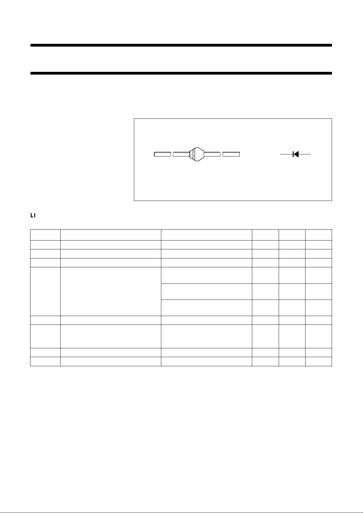
handbook, 2 columns
M3D118
BY328
Damper diode
Product specification
Supersedes data of May 1996
File under Discrete Semiconductors, SC01
1996 Sep 30
Philips Semiconductors Product specification
Damper diode BY328
FEATURES
• Glass passivated
• High maximum operating
DESCRIPTION
Rugged glass package, using a high
temperature alloyed construction.
This package is hermetically sealed
and fatigue free as coefficients of
expansion of all used parts are
matched.
temperature
• Low leakage current
• Excellent stability
• Available in ammo-pack
ka
• Also available with preformed leads
for easy insertion.
2/3 page (Datasheet)
MAM104
APPLICATIONS
• Damper diode in high frequency
horizontal deflection circuits up to
Fig.1 Simplified outline (SOD64) and symbol.
38 kHz.
LIMITING VALUES
In accordance with the Absolute Maximum Rating System (IEC 134).
SYMBOL PARAMETER CONDITIONS MIN. MAX. UNIT
V
RSM
V
RRM
V
R
I
FWM
non-repetitive peak reverse voltage − 1500 V
repetitive peak reverse voltage − 1500 V
continuous reverse voltage − 1400 V
working peak forward current Ttp=55°C; lead length = 10 mm
− 6.0 A
see Fig.2
=55°C; PCB mounting (see
T
amb
− 4.7 A
Fig.5); see Fig.2
T
=55°C; PCB mounting (see
amb
− 3.0 A
Fig.4); see Fig 2
I
FRM
I
FSM
T
T
stg
j
repetitive peak forward current − 10 A
non-repetitive peak forward current t = 10 ms half sinewave;
Tj=T
VR=V
prior to surge;
j max
RRMmax
− 60 A
storage temperature −65 +175 °C
junction temperature −65 +150 °C
1996 Sep 30 2
Philips Semiconductors Product specification
Damper diode BY328
ELECTRICAL CHARACTERISTICS
T
=25°C; unless otherwise specified.
j
SYMBOL PARAMETER CONDITIONS MAX. UNIT
V
F
I
R
t
rr
t
fr
THERMAL CHARACTERISTICS
SYMBOL PARAMETER CONDITIONS VALUE UNIT
R
th j-tp
R
th j-a
forward voltage IF= 5 A; Tj=T
= 5 A; see Fig.3 1.45 V
I
F
reverse current VR=V
; Tj= 150 °C 150 µA
Rmax
reverse recovery time when switched from IF= 0.5 A to
; see Fig.3 1.35 V
j max
500 ns
IR= 1 A; measured at IR= 0.25 A;
see Fig.6
forward recovery time when switched to IF= 5 A in 50 ns;
Tj=T
; see Fig.7
j max
500 ns
thermal resistance from junction to tie-point lead length = 10 mm 25 K/W
thermal resistance from junction to ambient note 1 75 K/W
mounted as shown in Fig.5 40 K/W
Note
1. Device mounted on an epoxy-glass printed-circuit board, 1.5 mm thick; thickness of Cu-layer ≥40 µm, see Fig.4.
For more information please refer to the
“General Part of Handbook SC01”
.
1996 Sep 30 3
 Loading...