

Philips buw84 DATASHEETS

DISCRETE SEMICONDUCTORS
DATA SH EET
BUW84; BUW85
Silicon diffused power transistors
Product specification
Supersedes data of February 1996
File under Discrete Semiconductors, SC06
1997 Aug 14
Philips Semiconductors Product specification
Silicon diffused power transistors BUW84; BUW85
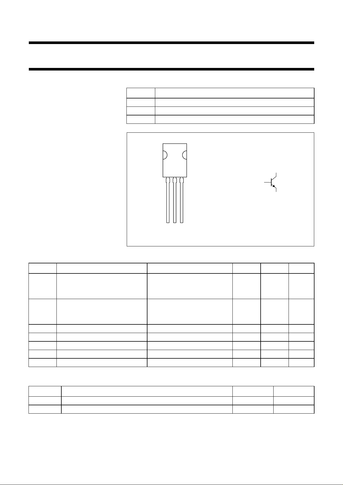
DESCRIPTION
High-voltage, high-speed,
glass-passivated NPN power
transistor in a SOT82 package.
APPLICATIONS
• Converters
• Inverters
• Switching regulators
• Motor control systems
• Switching applications.
PINNING
PIN DESCRIPTION
1 base
2 collector; connected to mounting base
3 emitter
k, halfpage
321
MBK107
Fig.1 Simplified outline (SOT82) and symbol.
MBB008
2
1
3
QUICK REFERENCE DATA
SYMBOL PARAMETER CONDITIONS TYP. MAX. UNIT
V
CESM
collector-emitter peak voltage VBE=0
BUW84 − 800 V
BUW85 − 1000 V
V
CEO
collector-emitter voltage open base
BUW84 − 400 V
BUW85 − 450 V
V
CEsat
I
C
I
CM
P
tot
t
f
collector-emitter saturation voltage IC= 1 A; IB= 200 mA; see Fig.7 − 1V
collector current (DC) see Figs 4 and 5 − 2A
collector current (peak value) see Figs 4 and 5 − 3A
total power dissipation Tmb≤ 25 °C; see Fig.8 − 50 W
fall time resistive load; see Fig.11 0.4 −µs
THERMAL CHARACTERISTICS
SYMBOL PARAMETER VALUE UNIT
R
th j-mb
R
th j-a
thermal resistance from junction to mounting base 2.1 K/W
thermal resistance from junction to ambient in free air 100 K/W
1997 Aug 14 1

Philips Semiconductors Product specification
Silicon diffused power transistors BUW84; BUW85
LIMITING VALUES
In accordance with the Absolute Maximum Rating System (IEC 134).
SYMBOL PARAMETER CONDITIONS MIN. MAX. UNIT
V
CESM
V
CEO
V
EBO
I
C
I
CM
I
B
I
BM
I
BM
P
tot
T
stg
T
j
collector-emitter peak voltage VBE=0
BUW84 − 800 V
BUW85 − 1000 V
collector-emitter voltage open base
BUW84 − 400 V
BUW85 − 450 V
emitter-base voltage open collector − 5V
collector current (DC) see Figs 4 and 5 − 2A
collector current (peak value) tp= 2 ms; see Figs 4 and 5 − 3A
base current (DC) − 0.75 A
base current (peak value) − 1A
base current (reversed; peak value) turn-off current −−1A
total power dissipation Tmb≤ 25 °C; see Fig.8 − 50 W
storage temperature −65 +150 °C
junction temperature − 150 °C
CHARACTERISTICS
=25°C unless otherwise specified.
T
j
SYMBOL PARAMETER CONDITIONS MIN. TYP. MAX. UNIT
V
CEOsust
collector-emitter sustaining voltage IC= 100 mA; I
BUW84 400 −−V
L = 25 mH; see Figs 2 and 3
Boff
=0;
BUW85 450 −−V
V
CEsat
collector-emitter saturation voltage IC= 0.3 A; IB=30mA;
−−0.8 V
see Fig.7
I
= 1 A; IB= 200 mA;
C
−−1V
see Fig.7
V
BEsat
I
CES
base-emitter saturation voltage IC= 1 A; IB= 200 mA −−1.1 V
collector-emitter cut-off current V
CEM=VCEMSmax
; VBE=0;
−−200 µA
note 1
V
CEM=VCEMSmax
; VBE=0;
−−1.5 mA
Tj= 125 °C; note 1
I
EBO
h
FE
emitter-base cut-off current VEB=5V; IC=0 −−1mA
DC current gain VCE=5V; IC= 5 A; see Fig.10 15 −−
V
=5V; IC= 100 mA;
CE
20 50 100
see Fig.10
f
T
transition frequency VCE=10V; IC= 200 mA;
− 20 − MHz
f = 1 MHz
1997 Aug 14 2
Philips Semiconductors Product specification
Silicon diffused power transistors BUW84; BUW85
SYMBOL PARAMETER CONDITIONS MIN. TYP. MAX. UNIT
Switching times in horizontal deflection circuit (see Fig.11)
t
on
t
s
t
f
turn-on time I
storage time I
fall time I
Note
1. Measured with a half-sinewave voltage (curve tracer).
= 1 A; I
Con
I
= −400 mA; VCC= 250 V
Boff
= 1 A; I
Con
I
= −400 mA; VCC= 250 V
Boff
= 1 A; I
Con
I
= −400 mA; VCC= 250 V
Boff
I
= 1 A; I
Con
= −400 mA; VCC= 250 V;
I
Boff
= 200 mA;
Bon
= 200 mA;
Bon
= 200 mA;
Bon
= 200 mA;
Bon
Tmb=95°C
− 0.2 0.5 µs
− 2 3.5 µs
− 0.4 −µs
−−1.4 µs
andbook, halfpage
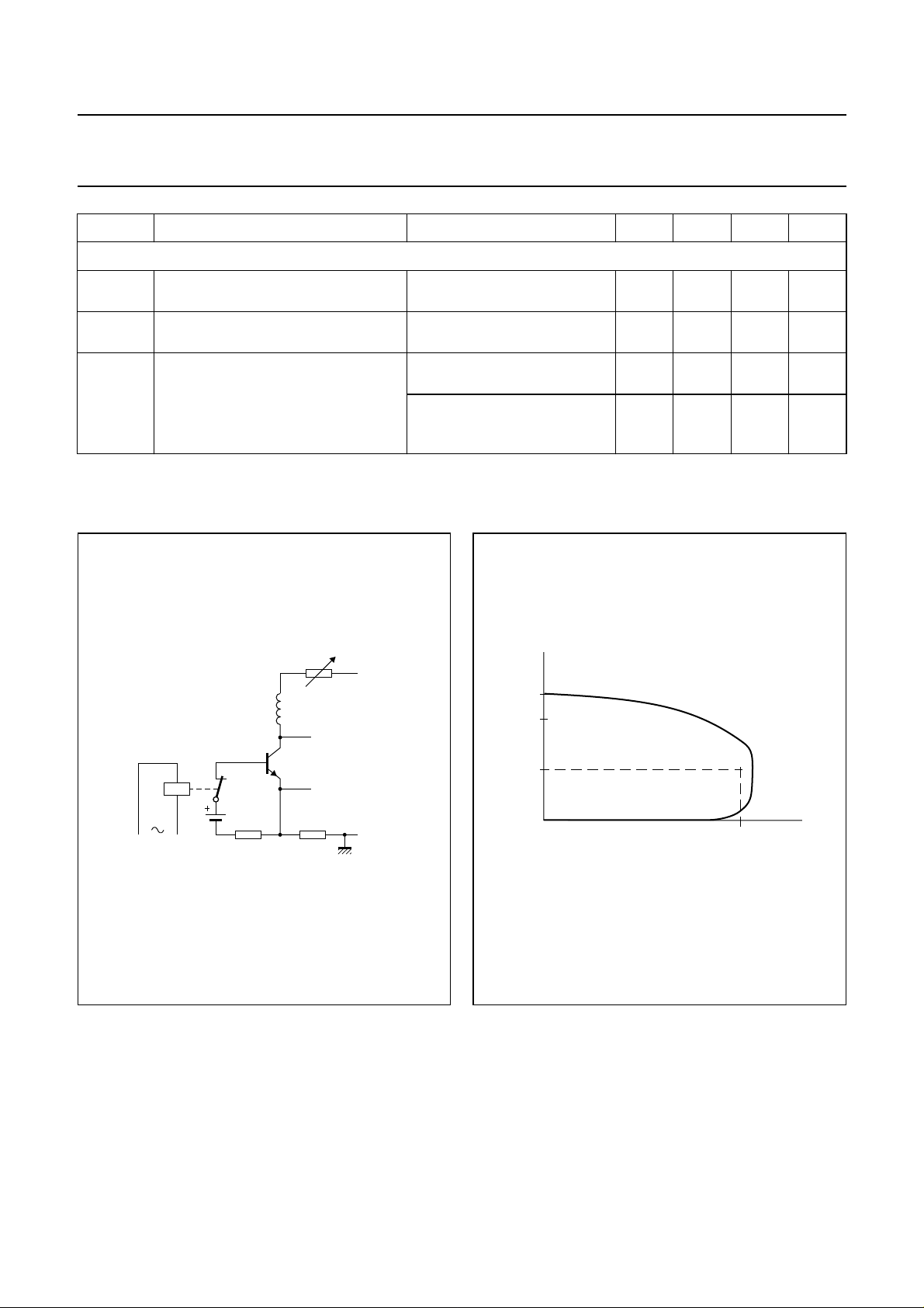
30 to 60 Hz
Fig.2 Test circuit for collector-emitter
100 to 200 Ω
L
300 Ω
6 V
sustaining voltage.
horizontal
oscilloscope
vertical
1 Ω
MGE252
+ 50 V
I
handbook, halfpage
C
(mA)
250
200
100
0
min
V
CEOsust
Fig.3 Oscilloscope display for collector-emitter
sustaining voltage.
MGE239
VCE (V)
1997 Aug 14 3
 Loading...