

Philips buw14 DATASHEETS

Philips Semiconductors Product specification
Silicon Diffused Power Transistor BUW14
GENERAL DESCRIPTION
High-voltage, high-speed, glass passivated npn power transistor in a SOT82 envelope intended for use in
converters, inverters, switching regulators, motor control systems and switching applications.
QUICK REFERENCE DATA
SYMBOL PARAMETER CONDITIONS TYP. MAX. UNIT
V
CESM
V
CEO
I
C
I
CM
P
tot
t
f
PINNING - SOT82 PIN CONFIGURATION SYMBOL
Collector-emitter voltage peak value VBE = 0 V - 1000 V
Collector-emitter voltage (open base) - 450 V
Collector current (DC) - 0.5 A
Collector current peak value - 1 A
Total power dissipation Tmb ≤ 60 ˚C - 20 W
Fall time 0.4 - µs
PIN DESCRIPTION
c
1 emitter
2 collector
b
3 base
23
1
LIMITING VALUES
Limiting values in accordance with the Absolute Maximum Rating System (IEC 134)
SYMBOL PARAMETER CONDITIONS MIN. MAX. UNIT
V
V
I
C
I
CM
I
B
I
BM
-I
P
T
T
CESM
CEO
BM
tot
stg
j
Collector-emitter voltage peak value VBE = 0 V - 1000 V
Collector-emitter voltage (open base) - 450 V
Collector current (DC) - 0.5 A
Collector current peak value - 1 A
Base current (DC) - 0.2 A
Base current peak value - 0.3 A
Reverse base current peak value
1
Total power dissipation Tmb ≤ 60 ˚C - 20 W
Storage temperature -65 150 ˚C
Junction temperature - 150 ˚C
THERMAL RESISTANCES
e
- 0.3 A
SYMBOL PARAMETER CONDITIONS TYP. MAX. UNIT
R
th j-mb
R
th j-a
1 Turn-off current.
Junction to mounting base - - 4.5 K/W
Junction to ambient in free air 100 - K/W
March 1992 1 Rev 1.000
Philips Semiconductors Product specification
Silicon Diffused Power Transistor BUW14
STATIC CHARACTERISTICS
Tmb = 25 ˚C unless otherwise specified
SYMBOL PARAMETER CONDITIONS MIN. TYP. MAX. UNIT
I
CES
I
CES
I
EBO
V
CEOsust
V
CEsat
V
CEsat
V
BEsat
h
FE
h
FE
Collector cut-off current
Emitter cut-off current VEB = 5 V; IC = 0 A - - 1.0 mA
Collector-emitter sustaining voltage IB = 0 A; IC = 100 mA; 450 - - V
Collector-emitter saturation voltages IC = 0.1 A; IB = 10 mA - - 0.8 V
Base-emitter saturation voltage IC = 0.2 A; IB = 20 mA - 1.0 V
DC current gain IC = 50 mA; VCE = 5 V - 50 -
DYNAMIC CHARACTERISTICS
Tmb = 25 ˚C unless otherwise specified
SYMBOL PARAMETER CONDITIONS TYP. MAX. UNIT
f
T
t
on
t
s
t
f
t
f
Transition frequency IC = 0.2 A; VCE = 10 V; f = 1 MHz 20 - MHz
Switching times (resistive load circuit) I
Turn-on time 0.4 0.7 µs
Turn-off storage time 3.5 5.0 µs
Turn-off fall time 0.4 - µs
Turn-off fall time Tmb = 95 ˚C - 1.3 µs
2
VBE = 0 V; VCE = V
VBE = 0 V; VCE = V
Tj = 125 ˚C
CESMmax
; - - 1.0 mA
CESMmax
- - 100 µA
L = 25 mH
IC = 0.2 A; IB = 20 mA - 1.0 V
IC = 300 mA; VCE = 5 V 25 50 100
= 0.2 A; I
Con
-I
= 40 mA; VCC = 250 V
Boff
= 20 mA;
Bon
100-200R
Horizontal
Oscilloscope
Vertical
300R
30-60 Hz
6V
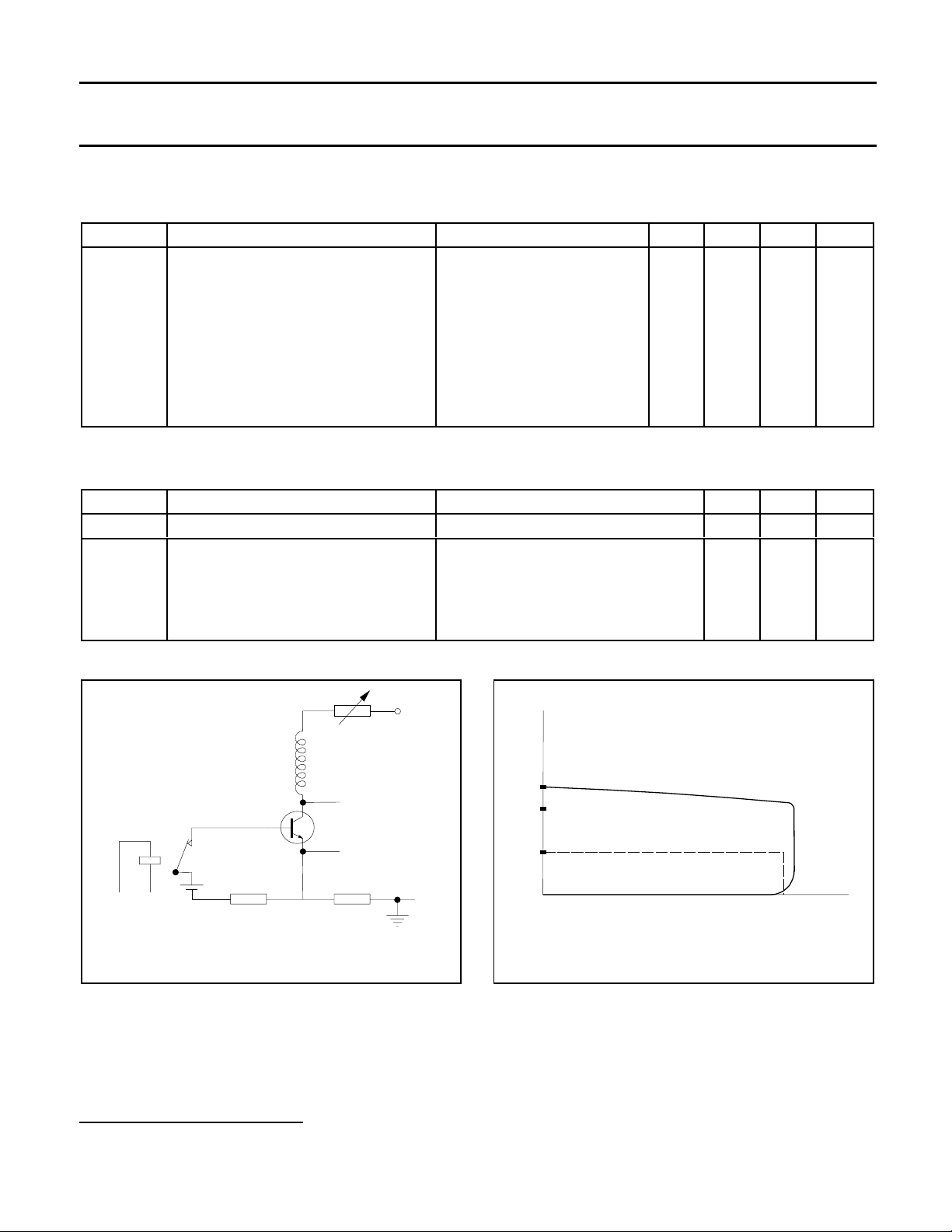
Fig.1. Test circuit for V
2 Measured with half sine-wave voltage (curve tracer).
1R
CEOsust
+ 50v
IC / mA
250
200
100
0
VCE / V
VCEOsust
. Fig.2. Oscilloscope display for V
min
CEOsust
.
March 1992 2 Rev 1.000
 Loading...