

Philips BUW13F, BUW13AF Datasheet

DISCRETE SEMICONDUCTORS
DATA SH EET
BUW13F; BUW13AF
Silicon diffused power transistors
Product specification
Supersedes data of February 1996
File under Discrete Semiconductors, SC06
1997 Aug 13
Philips Semiconductors Product specification
Silicon diffused power transistors BUW13F; BUW13AF
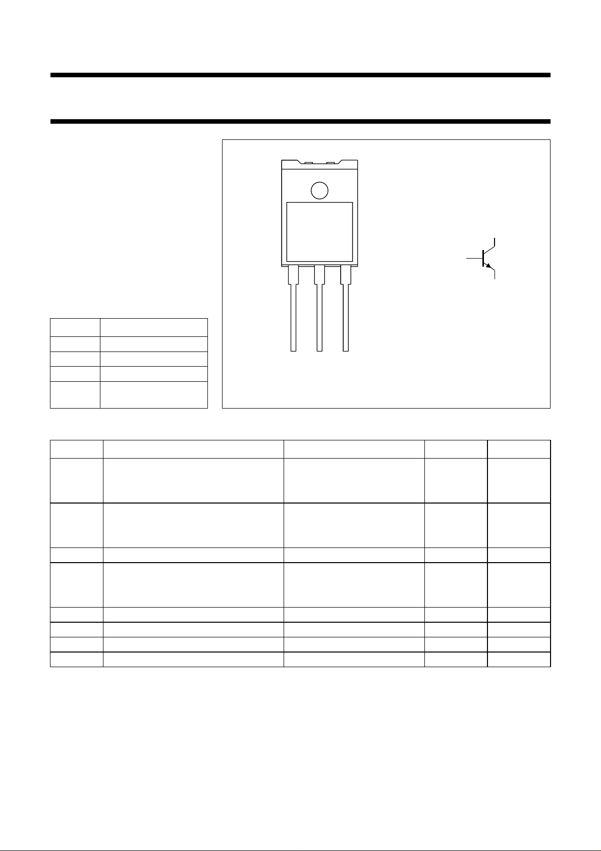
DESCRIPTION
High-voltage, high-speed,
ok, halfpage
glass-passivated NPN power
transistor in a SOT199 package.
APPLICATIONS
• Converters
handbook, halfpage
2
• Inverters
• Switching regulators
• Motor control systems.
1
MBB008
3
PINNING
PIN DESCRIPTION
1 base
2 collector
123
Front view
MSB012
3 emitter
mb mounting base;
Fig.1 Simplified outline (SOT199) and symbol.
electrically isolated
QUICK REFERENCE DATA
SYMBOL PARAMETER CONDITIONS MAX. UNIT
V
CESM
collector-emitter peak voltage VBE=0
BUW13F 850 V
BUW13AF 1000 V
V
CEO
collector-emitter voltage open base
BUW13F 400 V
BUW13AF 450 V
V
I
Csat
CEsat
collector-emitter saturation voltage see Figs 8 and 10 1.5 V
collector saturation current
BUW13F 10 A
BUW13AF 8 A
I
I
P
t
C
CM
tot
f
collector current (DC) see Figs 3 and 4 15 A
collector current (peak value) tp< 20 ms; see Fig 4 30 A
total power dissipation Th≤ 25 °C; see Fig.2 37 W
fall time resistive load; see Fig.13 0.8 µs
1997 Aug 13 2

Philips Semiconductors Product specification
Silicon diffused power transistors BUW13F; BUW13AF
THERMAL CHARACTERISTICS
SYMBOL PARAMETER CONDITIONS VALUE UNIT
R
th j-h
R
th j-a
Notes
1. Mounted without heatsink compound and 30 ±5 N force on centre of package.
2. Mounted with heatsink compound and 30 ±5 N force on centre of package.
LIMITING VALUES
In accordance with the Absolute Maximum Rating System (IEC 134).
SYMBOL PARAMETER CONDITIONS MIN. MAX. UNIT
V
CESM
V
CEO
I
Csat
I
C
I
CM
I
B
I
BM
P
tot
T
stg
T
j
thermal resistance from junction to external heatsink note 1 3.4 K/W
note 2 2.5 K/W
thermal resistance from junction to ambient 35 K/W
collector-emitter peak voltage VBE=0
BUW13F − 850 V
BUW13AF − 1000 V
collector-emitter voltage open base
BUW13F − 400 V
BUW13AF − 450 V
collector saturation current
BUW13F − 10 A
BUW13AF − 8A
collector current (DC) see Figs 3 and 4 − 15 A
collector current (peak value) tp< 20 ms; see Fig 4 − 30 A
base current (DC) − 6A
base current (peak value) tp= −20 ms − 9A
total power dissipation Th≤ 25 °C; see Fig.2; note 1 − 37 W
T
≤ 25 °C; see Fig.2; note 2 − 50 W
h
storage temperature −65 +150 °C
junction temperature − 150 °C
Notes
1. Mounted without heatsink compound and 30 ±5 N force on centre of package.
2. Mounted with heatsink compound and 30 ±5 N force on centre of package.
ISOLATION CHARACTERISTICS
SYMBOL PARAMETER MAX. UNIT
V
C
isolM
isol
isolation voltage from all terminals to external heatsink (peak value); note 1 2000 V
isolation capacitance from collector to external heatsink 21 pF
Note
1. Repetitive peak operation with RH ≤ 65% under clean and dust-free conditions.
1997 Aug 13 3

Philips Semiconductors Product specification
Silicon diffused power transistors BUW13F; BUW13AF
CHARACTERISTICS
T
=25°C unless otherwise specified.
j
SYMBOL PARAMETER CONDITIONS MIN. TYP. MAX. UNIT
V
CEOsust
V
CEsat
V
BEsat
I
Csat
I
CES
I
EBO
h
FE
collector-emitter sustaining voltage IC= 100 mA; I
BUW13F 400 −−V
L = 25 mH; see Figs 6 and 7
BUW13AF 450 −−V
collector-emitter saturation voltage
BUW13F I
= 10 A; IB= 2 A; see
C
Figs 8 and 10
BUW13AF I
= 8 A; IB= 1.6 A; see
C
Figs 8 and 10
base-emitter saturation voltage
BUW13F I
BUW13AF I
= 10 A; IB= 2 A; see Fig.8 −−1.6 V
C
= 8 A; IB= 1.6 A;
C
see Fig.8
collector saturation current VCE= 1.5 V
BUW13F −−10 A
BUW13AF −−8A
collector-emitter cut-off current VCE=V
CESMmax
note 1
V
CE=VCESMmax
Tj= 125 °C; note 1
emitter-base cut-off current VEB=9V; IC=0 −−10 mA
DC current gain VCE=5V; IC= 20 mA;
see Fig.11
V
=5V; IC= 1.5 A;
CE
see Fig.11
=0;
Boff
; VBE=0;
; VBE=0;
−−1.5 V
−−1.5 V
−−1.6 V
−−1mA
−−4mA
10 18 35
10 20 35
Switching times resistive load (see Figs 12 and 13)
t
on
t
s
t
f
turn-on time
BUW13F I
BUW13AF I
storage time
BUW13F I
BUW13AF I
fall time
BUW13F I
BUW13AF I
Con
Con
Con
Con
Con
Con
= 10 A; I
= 8 A; I
= 10 A; I
= 8 A; I
= 10 A; I
= 8 A; I
Switching times inductive load (see Figs 14 and 15)
t
s
storage time
BUW13F I
= 10 A; IB=2A;
Con
VCL= 250 V; Tc= 100 °C
BUW13AF I
= 8 A; IB= 1.6 A;
Con
VCL= 300 V; Tc= 100 °C
1997 Aug 13 4
Bon=IBoff
Bon=IBoff
Bon=IBoff
Bon=IBoff
Bon=IBoff
Bon=IBoff
=2A −−1µs
= 1.6 A −−1µs
=2A −−4µs
= 1.6 A −−4µs
=2A −−0.8 µs
= 1.6 A −−0.8 µs
− 2.8 3.5 µs
− 2.8 3.5 µs
Philips Semiconductors Product specification
Silicon diffused power transistors BUW13F; BUW13AF
SYMBOL PARAMETER CONDITIONS MIN. TYP. MAX. UNIT
t
f
Note
1. Measured with a half-sinewave voltage (curve tracer).
fall time
BUW13F I
BUW13AF I
= 10 A; IB=2A;
Con
VCL= 250 V; Tc= 100 °C
= 8 A; IB= 1.6 A;
Con
VCL= 300 V; Tc= 100 °C
− 200 300 ns
− 200 300 ns
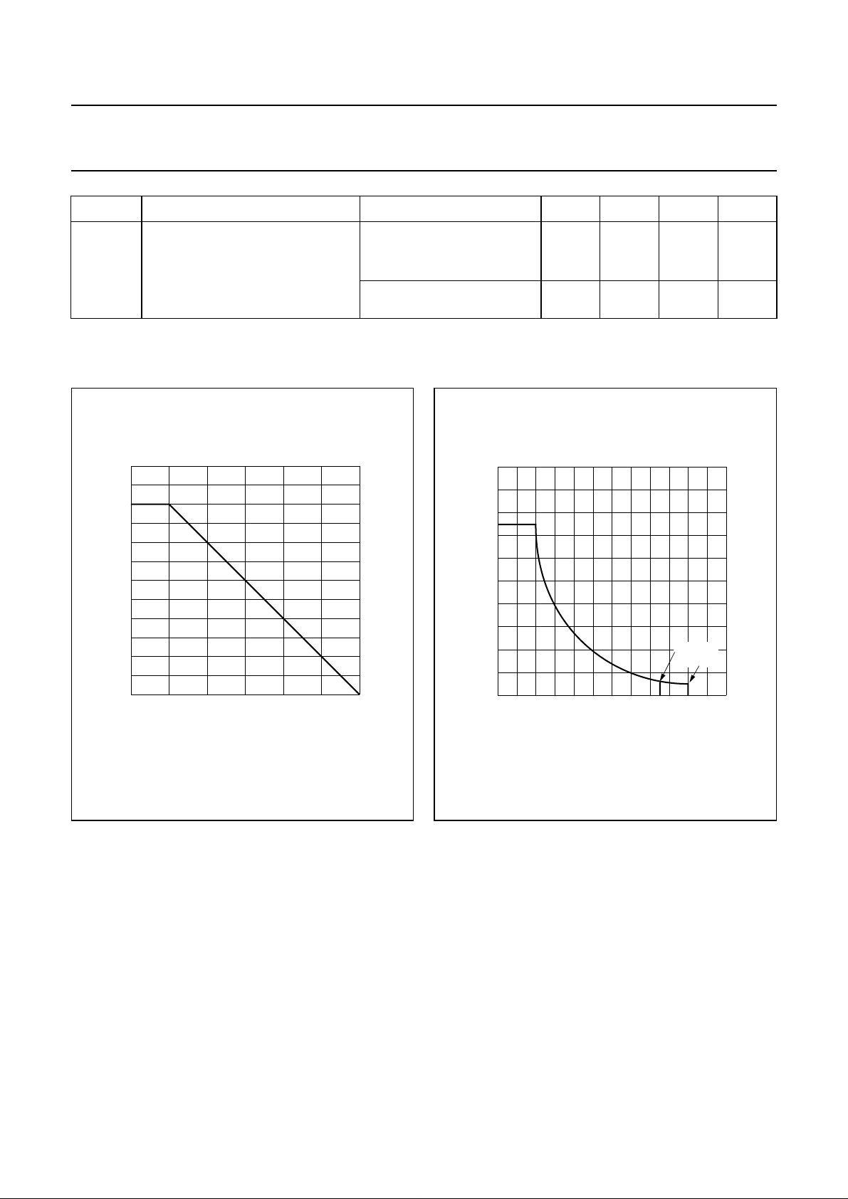
120
handbook, halfpage
P
tot max
(%)
80
40
0
050
100 150
T
h
Fig.2 Power derating curve.
o
(
MGK674
C)
20
handbook, halfpage
I
C
(A)
10
0
0 400
Tc≤ 100°C; VBE= −1to−5V.
Fig.3 Reverse bias SOAR.
800
MGB896
BUW13F
BUW13AF
VCE (V)
1200
1997 Aug 13 5
 Loading...