

Philips BUT211X Datasheet
Philips Semiconductors Product specification
Silicon Diffused Power Transistor BUT211X
GENERAL DESCRIPTION
Enhanced performance, new generation, high speed switching npn transistor in a plastic full-pack envelope
specially suited for high frequency electronic lighting ballast applications.
QUICK REFERENCE DATA
SYMBOL PARAMETER CONDITIONS TYP. MAX. UNIT
V
CESM
V
CEO
I
C
I
CM
P
tot
V
CEsat
t
f
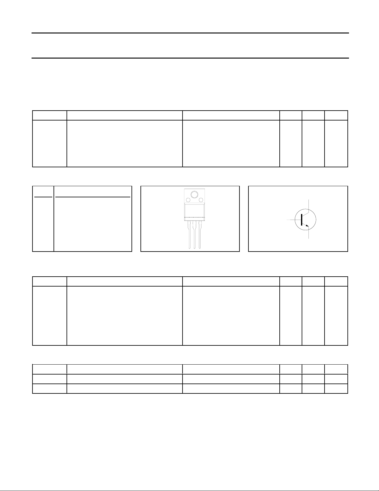
PINNING - SOT186A PIN CONFIGURATION SYMBOL
Collector-emitter voltage peak value VBE = 0 V - 850 V
Collector-emitter voltage (open base) - 400 V
Collector current (DC) - 5 A
Collector current peak value - 10 A
Total power dissipation Ths ≤ 25 ˚C - 32 W
Collector-emitter saturation voltage IC = 3.0 A; IB = 0.4 A - 2.0 V
Inductive fall time I
= 3.0 A; I
Con
= 0.3 A - 0.1 µs
Bon
PIN DESCRIPTION
case
c
1 base
2 collector
b
3 emitter
case isolated
LIMITING VALUES
Limiting values in accordance with the Absolute Maximum Rating System (IEC 134)
SYMBOL PARAMETER CONDITIONS MIN. MAX. UNIT
V
V
I
C
I
CM
I
B
I
BM
P
T
T
CESM
CEO
tot
stg
j
Collector-emitter voltage peak value VBE = 0 V - 850 V
Collector-emitter voltage (open base) - 400 V
Collector current (DC) - 5 A
Collector current peak value - 10 A
Base current (DC) - 2 A
Base current peak value - 4 A
Total power dissipation Ths ≤ 25 ˚C - 32 W
Storage temperature -65 150 ˚C
Junction temperature - 150 ˚C
THERMAL RESISTANCES
SYMBOL PARAMETER CONDITIONS TYP. MAX. UNIT
R
R
th j-hs
th j-a
Junction to heat sink - 3.95 K/W
Junction to ambient in free air - 55 K/W
123
e
March 1996 1 Rev 1.000

Philips Semiconductors Product specification
Silicon Diffused Power Transistor BUT211X
ISOLATION LIMITING VALUE & CHARACTERISTIC
Ths = 25 ˚C unless otherwise specified
SYMBOL PARAMETER CONDITIONS MIN. TYP. MAX. UNIT
V
isol
C
isol
STATIC CHARACTERISTICS
Ths = 25 ˚C unless otherwise specified
SYMBOL PARAMETER CONDITIONS MIN. TYP. MAX. UNIT
I
CES
I
CES
I
EBO
V
CEOsust
V
CEsat
V
BEsat
h
FE
h
FE
h
FE
R.M.S. isolation voltage from all f = 50-60 Hz; sinusoidal - 2500 V
three terminals to external waveform;
heatsink R.H. ≤ 65% ; clean and dustfree
Capacitance from T2 to external f = 1 MHz - 10 - pF
heatsink
Collector cut-off current
1
VBE = 0 V; VCE = V
VBE = 0 V; VCE = V
Tj = 125 ˚C
CESMmax
; - - 2.0 mA
CESMmax
- - 1.0 mA
Emitter cut-off current VEB = 9.0 V; IC = 0 A - - 10.0 mA
Collector-emitter sustaining voltage IB = 0 A; IC = 100 mA; 400 - - V
L = 25 mH
Collector-emitter saturation voltage IC = 3.0 A; IB = 0.4 A - 0.8 2.0 V
Base-emitter saturation voltage IC = 3.0 A; IB = 0.4 A - - 1.3 V
DC current gain IC = 1.0 A; VCE = 2 V 13 21 30
IC = 3.0 A; VCE = 2 V 7.5 11 Gain bands
2
1IC = 1.0 A; VCE = 2 V 13 - 20
(Acceptance limits) 2 18 - 25
323 -30
DYNAMIC CHARACTERISTICS
Ths = 25 ˚C unless otherwise specified
SYMBOL PARAMETER CONDITIONS TYP. MAX. UNIT
Switching times resistive load I
t
s
t
f
Turn-off storage time 1.5 2.0 µs
Turn-off fall time 0.5 0.8 µs
Switching times inductive load I
t
s
t
f
t
s
t
f
1 Measured with half sine-wave voltage (curve tracer).
2 Gain Banding.
Product is divided into 3 gain bands for matching purposes.
The gain band is printed on the device.
All devices within a device rail will be from the same gain band.
However, a box may contain rails from more than one band.
Band quantities are shown on the box label.
It is not possible to order specific gain bands.
Turn-off storage time 1.0 1.2 µs
Turn-off fall time 60 100 ns
Turn-off storage time 1.1 1.4 µs
Turn-off fall time 120 250 ns
= 3.0 A; I
Con
= 3.0 A; I
Con
-V
= 5 V
BB
I
= 3.0 A; I
Con
-V
= 5 V; Tj = 100 ˚C
BB
= 0.3 A; -I
Bon
= 0.3 A; LB = 1 µH;
Bon
= 0.3 A; LB = 1 µH;
Bon
Boff
= 0.6 A
March 1996 2 Rev 1.000
Philips Semiconductors Product specification
Silicon Diffused Power Transistor BUT211X
ICon
90 %
10 %
tf
IBon
30-60 Hz
6V
300R
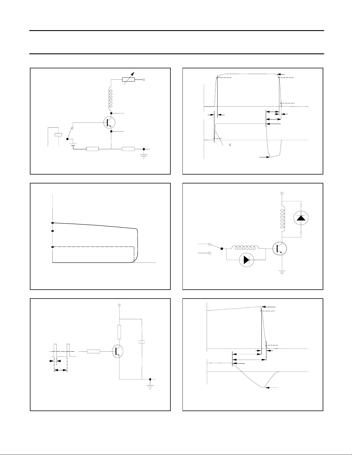
Fig.1. Test circuit for V
100-200R
Horizontal
Oscilloscope
Vertical
1R
.
CEOsust
+ 50v
90 %
IC
ton
IB
10 %
tr 30ns
-IBoff
ts
toff
Fig.4. Switching times waveforms with resistive load.
IC / mA
250
200
100
0
VCE / V
Fig.2. Oscilloscope display for V
VIM
0
tp
T
R
B
min
VCEOsust
VCC
R
L
T.U.T.
CEO
sust
VCC
LC
IBon
-VBB
.
Fig.5. Test circuit inductive load.
LB
T.U.T.
VCC = 300 V; -VBE = 5 V;LB = 1 uH
ICon
90 %
IC
10 %
ts
toff
IB
IBon
tf
t
t
-IBoff
Fig.3. Test circuit resistive load. VIM = -6 to +8 V
Fig.6. Switching times waveforms with inductive load.
VCC = 250 V; tp = 20 µs; δ = tp / T = 0.01.
RB and RL calculated from I
Con
and I
requirements.
Bon
March 1996 3 Rev 1.000
 Loading...