

Page 1

Philips Semiconductors Product specification
TOPFET dual high side switch BUK218-50DC
QUICK REFERENCE DATA
DESCRIPTION
Monolithic dual channel high side SYMBOL PARAMETER MIN. UNIT
protected power switch in
TOPFET2 technology assembled in I
a 7 pin plastic surface mount
L
package.
SYMBOL PARAMETER MAX. UNIT
APPLICATIONS
V
General purpose switch for driving I
lamps, motors, solenoids, heaters. T
BG
L
j
R
ON
FEATURES FUNCTIONAL BLOCK DIAGRAM
Nominal load current (ISO) 8 A
Continuous off-state supply voltage 50 V
Continuous load current 16 A
Continuous junction temperature 150 ˚C
On-state resistance, Tj = 25˚C 40 mΩ
Vertical power TrenchMOS
Low on-state resistance
INPUT 1
CMOS logic compatible
Very low quiescent current
Overtemperature protection
Load current limiting
INPUT 2
Overload and
short circuit protection
Self resetting overcurrent
protection
Overvoltage and undervoltage
shutdown with hysteresis
Off-state open circuit
load detection
STATUS
CONTROL &
PROTECTION
CIRCUITS
Diagnostic status indication
Voltage clamping for turn off
of inductive loads
ESD protection on all pins
GROUND
RG
Reverse battery, overvoltage
and transient protection
Fig.1. Elements of the TOPFET dual HSS with internal ground resistor.
PINNING - SOT427 PIN CONFIGURATION SYMBOL
PIN DESCRIPTION
1 load 1
2 ground
3 input 1
4 connected to mb
5 status
6 input 2
7 load 2
1234567
mb battery Fig. 2. Fig. 3.
mb
I1
I2
S
B
DUAL
HSTF
G
BATT
LOAD 1
LOAD 2
L1
L2
CONVENTION
Positive currents flow into pins, except for load and ground pins.
October 2001 1 Rev 2.010
Page 2

Philips Semiconductors Product specification
TOPFET dual high side switch BUK218-50DC
LIMITING VALUES
Limiting values in accordance with the Absolute Maximum System (IEC 134)
SYMBOL PARAMETER CONDITIONS MIN. MAX. UNIT
V
BG
I
L
P
D
T
stg
T
j
V
GB
V
GB
RI, R
I
I
I
S
I
I
I
S
Continuous supply voltage 0 50 V
Continuous load current per channel T
Total power dissipation T
135˚C - 8 A
mb ≤
25˚C - 83.3 W
mb ≤
Storage temperature -55 175 ˚C
Continuous junction temperature
Reverse battery voltages
1
2
-40 150 ˚C
Continuous reverse voltage - 16 V
Peak reverse voltage - 32 V
Application information
S
External resistors
3
to limit input, status currents 3.2 - kΩ
Input and status currents
Continuous input current -5 5 mA
Continuous status current -5 5 mA
Repetitive peak input current δ ≤ 0.1, tp = 300 µs -50 50 mA
Repetitive peak status current δ ≤ 0.1, tp = 300 µs -50 50 mA
Inductive load clamping VBG = 13 V, IL = 8 A
E
BL
Non-repetitive clamping energy (one Tj = 150˚C prior to turn-off - 150 mJ
channel)
ESD LIMITING VALUE
SYMBOL PARAMETER CONDITIONS MIN. MAX. UNIT
V
C
1 For normal continuous operation. A higher Tj is allowed as an overload condition but at the threshold T
2 Reverse battery voltage is allowed only with external resistors to ensure that the input and status currents do not exceed the limiting values.
3 To limit currents during reverse battery and transient overvoltages (positive or negative).
October 2001 2 Rev 2.010
Electrostatic discharge capacitor Human body model; - 2 kV
voltage C = 250 pF; R = 1.5 kΩ
the over temperature trip operates
to protect the switch.
The internal ground resistor limits the reverse battery ground current. The connected loads must limit the reverse load currents. Power
is dissipated and the Tj rating must be observed.
j(TO)
Page 3

Philips Semiconductors Product specification
TOPFET dual high side switch BUK218-50DC
THERMAL CHARACTERISTIC
SYMBOL PARAMETER CONDITIONS MIN. TYP. MAX. UNIT
Thermal resistance
1
R
th j-mb
Junction to mounting base per channel - 2.4 3 K/W
both channels - 1.2 1.5 K/W
STATIC CHARACTERISTICS
Limits are at -40˚C ≤ Tmb ≤ 150˚C and typicals at Tmb = 25 ˚C unless otherwise stated
SYMBOL PARAMETER CONDITIONS MIN. TYP. MAX. UNIT
Clamping voltages
V
BG
V
BL
V
GL
V
BG
I
B
I
L
I
G
I
L
Battery to ground IG = 1 mA 45 55 65 V
Battery to load per channel IL = IG = 1 mA 50 55 65 V
Ground to load
2
IL = 10 mA 18 23 28 V
IL = 10 A; tp = 300 µs202530V
Supply voltage battery to ground
Operating range
3
- 5.5 - 35 V
Currents 9 V ≤ VBG ≤ 35 V
Total quiescent current
4
VLG = 0 V - - 20 µA
Tmb = 25˚C - 0.1 1 µA
Off-state load current per VBL = V
BG
--10µA
channel Tmb = 25˚C - 0.1 1 µA
Operating current one channel on - 1.8 3 mA
both channels on - 3.6 6 mA
Nominal load current
5
VBL = 0.5 V; Tmb = 85˚C 8 - - A
R
G
R
ON
Effective internal ground IG = -200 mA; tp = 300 µs 40 75 100 Ω
resistance
Resistances per channel V
6
BG
I
L
7
t
p
T
j
On-state resistance 9 to 35 V 10 A 300 µs 25˚C - 30 40 mΩ
150˚C - 60 80 mΩ
R
ON
On-state resistance 5.5 V 5 A 300 µs 25˚C - 50 60 mΩ
150˚C - 100 120 mΩ
1 Of the output Power MOS transistors.
2 For a high side switch, the load pin voltage goes negative with respect to ground during the turn-off of an inductive load. This negative voltage
3 On-state resistance is increased if the supply voltage is less than 7 V.
4 This is the continuous current drawn from the battery when both inputs are low and includes leakage currents to the loads.
5 Per channel but with both channels conducting. Defined as in ISO 10483-1.
6 Equivalent of the parallel connected resistors for both channels.
7 The supply and input voltage for the RON tests are continuous. The specified pulse duration tp refers only to the applied load current.
is clamped by the device.
October 2001 3 Rev 2.010
Page 4

Philips Semiconductors Product specification
TOPFET dual high side switch BUK218-50DC
INPUT CHARACTERISTICS
5.5 V ≤ VBG ≤ 35 V. Limits are at -40˚C ≤ Tmb ≤ 150˚C and typicals at Tmb = 25˚C unless otherwise stated.
SYMBOL PARAMETER CONDITIONS MIN. TYP. MAX. UNIT
I
I
V
IG
V
IG(ON)
V
IG(OFF)
∆V
I
I(ON)
I
I(OFF)
IG
Input current VIG = 5 V 20 60 160 µA
Input clamping voltage II = 200 µA 5.5 7 8.5 V
Input turn-on threshold voltage - 2.1 3 V
Input turn-off threshold voltage 1.2 1.8 - V
Input turn-on hysteresis 0.15 0.3 0.5 V
Input turn-on current VIG = 3 V - - 100 µA
Input turn-off current VIG = 1.2 V 12 - - µA
OPEN CIRCUIT DETECTION CHARACTERISTICS
An open circuit load on either channel can be detected in the off-state. Refer to TRUTH TABLE.
This feature requires external load pull-up to a positive supply voltage via a suitable resistor.
Limits are at -40˚C ≤ Tmb ≤ 150˚C and typical is at Tmb = 25˚C.
SYMBOL PARAMETER CONDITIONS MIN. TYP. MAX. UNIT
Open circuit detection
V
LG(OC)
I
B(OC)
Load ground threshold voltage VBG ≥ 9 V 1.5 2.5 3.5 V
Supply quiescent current per VBG = VLG = 16 V - 0.8 1.5 mA
OC channel open circuit detected,
other channel off
-I
L(OC)
Load ground current per VLG = 16 V - 200 300 µA
channel VLG = 3.5 V - 22 40 µA
t
d(OC)
Status delay time input low to status low - 65 100 µs
Application information
R
ext
External load pull-up resistance V
= 5 V - 10 - kΩ
ext
per channel
October 2001 4 Rev 2.010
Page 5

Philips Semiconductors Product specification
TOPFET dual high side switch BUK218-50DC
UNDERVOLTAGE & OVERVOLTAGE CHARACTERISTICS
Limits are at -40˚C ≤ Tmb ≤ 150˚C and typicals at Tmb = 25˚C. Refer to TRUTH TABLE.
SYMBOL PARAMETER CONDITIONS MIN. TYP. MAX. UNIT
Undervoltage
V
BG(UV)
Low supply threshold voltage
1
2 4.2 5.3 V
∆V
BG(UV)
Hysteresis 0.1 0.5 1 V
Overvoltage
V
BG(OV)
∆V
I
BG(OV)
BG(OV)
High supply threshold voltage
Hysteresis 0.4 1 2 V
Operating current per channel VBG > V
2
BG(OV)
35 40 45 V
-12mA
OVERLOAD PROTECTION CHARACTERISTICS
Independent protection per channel. Refer to TRUTH TABLE.
5.5 V ≤ VBG ≤ 35 V, limits are at -40˚C ≤ Tmb ≤ 150˚C and typicals at Tmb = 25˚C unless otherwise stated.
SYMBOL PARAMETER CONDITIONS MIN. TYP. MAX. UNIT
Overload protection VBL = VBG; tp = 300 µs
I
L(lim)
P
T
D(TO)
DSC
Load current limiting VBG ≥ 8 V 18 30 42 A
VBG = 5.5 V 15 27 42 A
Short circuit load protection Tmb ≤ 125˚C prior to overload
Overload power threshold for protection
4
Characteristic time which determines trip time
3
100 150 200 W
5
- 200 500 µs
Overtemperature protection
T
j(TO)
∆T
j(TO)
1 Undervoltage sensors causes each channel to switch off and reset.
2 Overvoltage sensors causes each output channel to switch off to protect its load.
3 Above this temperature measurement of these parameters is prevented because OT protection may occur prior to SC protection.
4 Normal operation will be resumed when PD < P
5 Trip time t
6 After cooling below the reset temperature the channel will resume normal operation.
Threshold junction temperature 150 170 190 ˚C
Hysteresis
varies with overload dissipation PD according to the exponential model formula t
d sc
6
and Tj < T
D(TO)
j(TO)
.
≈ T
d sc
3 1020˚C
/ LN[ PD / P
DSC
D(TO)
].
October 2001 5 Rev 2.010
Page 6

Philips Semiconductors Product specification
TOPFET dual high side switch BUK218-50DC
STATUS CHARACTERISTICS
The status output is an open drain transistor, and requires an external pull-up circuit to indicate a logic high.
Limits are at -40˚C ≤ T
SYMBOL PARAMETER CONDITIONS MIN. TYP. MAX. UNIT
≤ 150˚C and typicals at Tmb = 25˚C unless otherwise stated. Refer to TRUTH TABLE.
mb
V
V
SG
SG(LO)
Status clamping voltage IS = 100 µA 5.5 7 8.5 V
Status low voltage IS = 100 µA - 0.7 0.9 V
IS = 250 µA - - 1.1 V
I
S
I
S(SAT)
Status leakage current VSG = 5 V - - 10 µA
T
= 25˚C - 0.1 1 µA
mb
Status saturation current
1
VSG = 5 V 5 10 15 mA
Application information
R
S
External pull-up resistor - 47 - kΩ
TRUTH TABLE
ABNORMAL CONDITIONS LOAD
INPUT DETECTED OUTPUT STATUS DESCRIPTION
SUPPLY LOAD 1 LOAD 2
1 2 UV OV OC SC OT OC SC OT 1 2
L L 0 X 0 X X 0 X X OFF OFF H both off & normal
L L 0 X 1 X X X X X OFF OFF L both off, one/both OC or short to V+
L H 0 X 1 X X 0 0 0 OFF ON L one off & OC, other on & normal
H L 0 0 0 0 0 0 0 0 ON OFF H one on & normal, other off & normal
H H 0 0 0 0 0 0 0 0 ON ON H both on & normal
H X 1 0 X X X 0 X X OFF OFF H supply undervoltage lockout
H X 0 1 X 0 0 X 0 0 OFF OFF H supply overvoltage shutdown
H X 0 0 0 1 X X X X OFF X L one SC shutdown
H L 0 0 0 1 X 0 0 X OFF OFF L one SC shutdown, other off & normal
H H 0 0 0 1 X 0 0 0 OFF ON L one SC shutdown, other on & normal
H X 0 0 0 0 1 X X X OFF X L one OT shutdown
H L 0 0 0 0 1 0 0 X OFF OFF L one OT shutdown, other off & normal
H H 0 0 0 0 1 0 0 0 OFF ON L one OT shutdown, other on & normal
KEY TO ABBREVIATIONS
L logic low UV undervoltage
H logic high OV overvoltage
X don’t care OC open circuit
0 condition not present SC short circuit
1 condition present OT overtemperature
1 For example with the pull-up resistor short circuited while the status transistor is conducting. This condition should be avoided in order to
October 2001 6 Rev 2.010
prevent possible interference with normal operation of the device.
Page 7

Philips Semiconductors Product specification
TOPFET dual high side switch BUK218-50DC
SWITCHING CHARACTERISTICS
Tmb = 25 ˚C, VBG = 13 V, for resistive load RL = 13 Ω per channel.
SYMBOL PARAMETER CONDITIONS MIN. TYP. MAX. UNIT
During turn-on from input going high
t
d on
dV/dt
Delay time to 10% V
Rate of rise of load voltage 30% to 70% V
on
L
L
-30-µs
0.5 1 2 V/µs
t
on
Total switching time to 90% V
L
- 100 400 µs
During turn-off from input going low
t
d off
dV/dt
t
off
Delay time to 90% V
Rate of fall of load voltage 70% to 30% V
off
Total switching time to 10% V
L
L
L
-20-µs
0.5 1 2 V/µs
- 40 200 µs
CAPACITANCES
Tmb = 25 ˚C; f = 1 MHz; VIG = 0 V
SYMBOL PARAMETER CONDITIONS MIN. TYP. MAX. UNIT
C
sg
C
ig
C
bl
Status capacitance VSG = 5 V - 11 15 pF
per channel
Input capacitance VBG = 13 V - 15 20 pF
Output capacitance VBL = 13 V - 265 375 pF
October 2001 7 Rev 2.010
Page 8
Philips Semiconductors Product specification
TOPFET dual high side switch BUK218-50DC
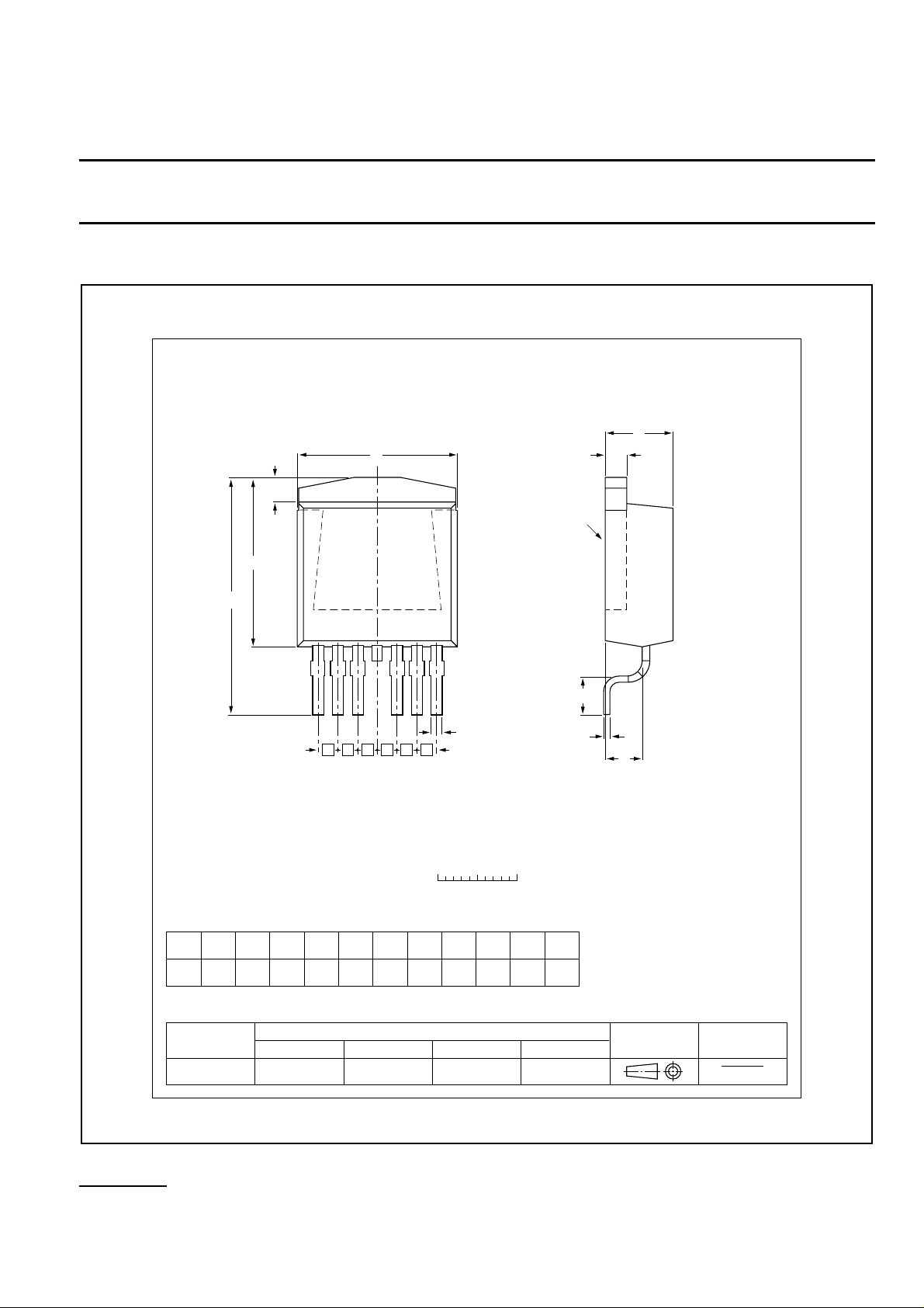
MECHANICAL DATA
Plastic single-ended surface mounted package (Philips version of D2-PAK);
7 leads (one lead cropped)
E
D
1
mounting
base
D
H
D
4
L
1
eeeeee
7
b
p
SOT427
A
A
1
c
Q
0 2.5 5 mm
scale
DIMENSIONS (mm are the original dimensions)
0.64
0.46
D
max.
11
D
1
10.30
1.60
9.70
1.20
REFERENCES
L
H
15.80
14.80
Q
D
2.60
2.20
EUROPEAN
PROJECTION
ISSUE DATE
99-06-25
01-04-18
E
1.27
2.90
2.10
p
UNIT
mm
A
4.50
4.10
OUTLINE
VERSION
SOT427
A
bc e
1
1.40
0.85
1.27
0.60
IEC JEDEC EIAJ
Fig.4. SOT427 surface mounting package1, centre pin connected to mounting base.
1 Epoxy meets UL94 V0 at 1/8". Net mass: 1.5 g.
For soldering guidelines and SMD footprint design, please refer to Data Handbook SC18.
October 2001 8 Rev 2.010
Page 9

Philips Semiconductors Product specification
TOPFET dual high side switch BUK218-50DC
DEFINITIONS
DATA SHEET STATUS
DATA SHEET PRODUCT DEFINITIONS
STATUS
Objective data Development This data sheet contains data from the objective specification for
Preliminary data Qualification This data sheet contains data from the preliminary specification.
Product data Production This data sheet contains data from the product specification. Philips
Limiting values
Limiting values are given in accordance with the Absolute Maximum Rating System (IEC 134). Stress above one
or more of the limiting values may cause permanent damage to the device. These are stress ratings only and
operation of the device at these or at any other conditions above those given in the Characteristics sections of
this specification is not implied. Exposure to limiting values for extended periods may affect device reliability.
Application information
Where application information is given, it is advisory and does not form part of the specification.
Philips Electronics N.V. 2001
All rights are reserved. Reproduction in whole or in part is prohibited without the prior written consent of the
copyright owner.
The information presented in this document does not form part of any quotation or contract, it is believed to be
accurate and reliable and may be changed without notice. No liability will be accepted by the publisher for any
consequence of its use. Publication thereof does not convey nor imply any license under patent or other
industrial or intellectual property rights.
1
STATUS
2
product development. Philips Semiconductors reserves the right to
change the specification in any manner without notice
Supplementary data will be published at a later date. Philips
Semiconductors reserves the right to change the specification without
notice, in order to improve the design and supply the best possible
product
Semiconductors reserves the right to make changes at any time in
order to improve the design, manufacturing and supply. Changes will
be communicated according to the Customer Product/Process
Change Notification (CPCN) procedure SNW-SQ-650A
LIFE SUPPORT APPLICATIONS
These products are not designed for use in life support appliances, devices or systems where malfunction of these
products can be reasonably expected to result in personal injury. Philips customers using or selling these products
for use in such applications do so at their own risk and agree to fully indemnify Philips for any damages resulting
from such improper use or sale.
1 Please consult the most recently issued datasheet before initiating or completing a design.
2 The product status of the device(s) described in this datasheet may have changed since this datasheet was published. The latest information is
October 2001 9 Rev 2.010
available on the Internet at URL http://www.semiconductors.philips.com.
 Loading...