

Philips BU2522DX Datasheet
Philips Semiconductors Product specification
Silicon Diffused Power Transistor BU2522DX
GENERAL DESCRIPTION
New generation, high-voltage, high-speed switching npn transistor with integrated damper diode in a plastic
full-pack envelope intended for use in horizontal deflection circuits of high resolution monitors. Features improved
RBSOA performance and is suitable for use in horizontal deflection circuits of pc monitors.
QUICK REFERENCE DATA
SYMBOL PARAMETER CONDITIONS TYP. MAX. UNIT
V
CESM
V
CEO
I
C
I
CM
P
tot
V
CEsat
I
Csat
V
F
t
f
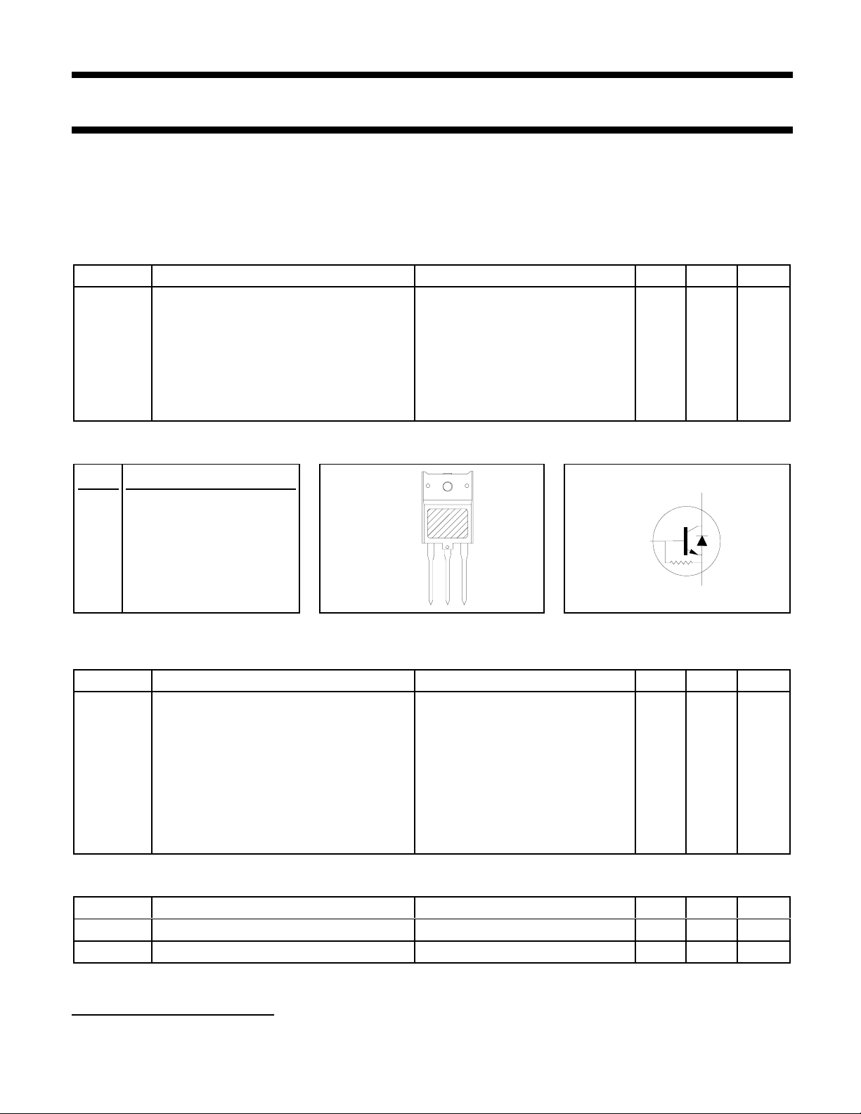
PINNING - SOT399 PIN CONFIGURATION SYMBOL
Collector-emitter voltage peak value VBE = 0 V - 1500 V
Collector-emitter voltage (open base) - 800 V
Collector current (DC) - 10 A
Collector current peak value - 25 A
Total power dissipation Ths ≤ 25 ˚C - 45 W
Collector-emitter saturation voltage IC = 6.0 A; IB = 1.2 A - 5.0 V
Collector saturation current f = 64 kHz 6 - A
Diode forward voltage IF = 6.0 A - 2.2 V
Fall time I
= 6.0 A; f = 64 kHz 0.12 0.25 µs
Csat
PIN DESCRIPTION
case
c
1 base
2 collector
b
3 emitter
case isolated
123
LIMITING VALUES
Limiting values in accordance with the Absolute Maximum Rating System (IEC 134)
SYMBOL PARAMETER CONDITIONS MIN. MAX. UNIT
V
CESM
V
CEO
I
C
I
CM
I
B
I
BM
-I
B(AV)
-I
BM
P
tot
T
stg
T
j
Collector-emitter voltage peak value VBE = 0 V - 1500 V
Collector-emitter voltage (open base) - 800 V
Collector current (DC) - 10 A
Collector current peak value - 25 A
Base current (DC) - 6 A
Base current peak value - 9 A
Reverse base current average over any 20 ms period - 150 mA
Reverse base current peak value
1
Total power dissipation Ths ≤ 25 ˚C - 45 W
Storage temperature -65 150 ˚C
Junction temperature - 150 ˚C
THERMAL RESISTANCES
Rbe
e
-6A
SYMBOL PARAMETER CONDITIONS TYP. MAX. UNIT
R
th j-hs
R
th j-a
1 Turn-off current.
Junction to heatsink with heatsink compound - 2.8 K/W
Junction to ambient in free air 35 - K/W
September 1997 1 Rev 1.200

Philips Semiconductors Product specification
Silicon Diffused Power Transistor BU2522DX
ISOLATION LIMITING VALUE & CHARACTERISTIC
Ths = 25 ˚C unless otherwise specified
SYMBOL PARAMETER CONDITIONS MIN. TYP. MAX. UNIT
V
isol
C
isol
STATIC CHARACTERISTICS
Ths = 25 ˚C unless otherwise specified
SYMBOL PARAMETER CONDITIONS MIN. TYP. MAX. UNIT
I
CES
I
CES
I
EBO
BV
EBO
R
be
V
CEOsust
V
CEsat
V
BEsat
h
FE
h
FE
V
F
Repetitive peak voltage from all R.H. ≤ 65 % ; clean and dustfree - 2500 V
three terminals to external
heatsink
Capacitance from T2 to external f = 1 MHz - 22 - pF
heatsink
Collector cut-off current
2
VBE = 0 V; VCE = V
VBE = 0 V; VCE = V
Tj = 125 ˚C
CESMmax
; - - 2.0 mA
CESMmax
- - 1.0 mA
Emitter cut-off current VEB = 7.5 V; IC = 0 A - 150 - mA
Emitter-base breakdown voltage IB = 600 mA 7.5 13.5 - V
Base-emitter resistance VEB = 7.5 V - 50 - Ω
Collector-emitter sustaining voltage IB = 0 A; IC = 100 mA; 800 - - V
L = 25 mH
Collector-emitter saturation voltage IC = 6.0 A; IB = 1.2 A - - 5.0 V
Base-emitter saturation voltage IC = 6.0 A; IB = 1.2 A - - 1.1 V
DC current gain IC = 1.0 A; VCE = 5 V - 13 -
IC = 6 A; VCE = 5 V 5 7 10
Diode forward voltage IF = 6 A - - 2.2 V
DYNAMIC CHARACTERISTICS
Ths = 25 ˚C unless otherwise specified
SYMBOL PARAMETER CONDITIONS TYP. MAX. UNIT
C
c
t
s
t
f
Collector capacitance IE = 0 A; VCB = 10 V; f = 1 MHz 115 - pF
Switching times (64 kHz line ICM = 6.0 A; LC = 170 µH; Cfb = 5.4 nF;
deflection circuit) I
= 0.7 A; LB = 0.6 µH; -VBB = 2 V;
B(end)
(-dIB/dt = 3.33 A / µs)
Turn-off storage time 1.7 2.0 µs
Turn-off fall time 0.12 0.25 µs
2 Measured with half sine-wave voltage (curve tracer).
September 1997 2 Rev 1.200
Philips Semiconductors Product specification
Silicon Diffused Power Transistor BU2522DX
ICsat
I end
B
t
t
t
V
I
I
CE
TRANSISTOR
C
B
DIODE
6.5 us5 us
16 us
Fig.1. Switching times waveforms (64 kHz).
ICsat
90 %
IC
10 %
IB
ts
IBend
tf
t
VCC
LC
IBend
-VBB
LB
Rbe
T.U.T.
VCL
CFB
Fig.4. Test Circuit RBSOA. VCC = 140 V; -VBB = 4 V;
LC = 100 - 400 µH; VCL ≤ 1500 V; LB = 3 µH;
CFB = 1 - 2.2 nF; IB(end) = 1.6 - 2 A
hFE
100
Tj = 25 C
5 V
10
1 V
Tj = 125 C
Fig.2. Switching times definitions.
IBend
-VBB
LB
D.U.T.
Fig.3. Switching times test circuit
+ 150 v nominal
adjust for ICsat
Rbe
Lc
- IBM
Cfb
t
1
0.1 10
IC / A
1001
Fig.5. Typical DC current gain. hFE = f (IC)
parameter V
VBESAT / V
1.2
1.1
1.0
0.9
0.8
0.7
0.6
0.5
0.4
0.1 1 10
.
Fig.6. Typical base-emitter saturation voltage.
Tj = 25 C
Tj = 125 C
VBEsat = f (IC); parameter IC/I
CE
IC/IB=
3
4
5
IC / A
B
September 1997 3 Rev 1.200
 Loading...