

Philips BT300M-600R, BT300M-500R, BT300S-800R, BT300S-600R, BT300S-500R Datasheet
...
Philips Semiconductors Product specification
Thyristors BT300S series
GENERAL DESCRIPTION QUICK REFERENCE DATA
Glasspassivatedthyristorsinaplastic SYMBOL PARAMETER MAX. MAX. MAX. UNIT
envelope, suitable for surface
mounting, intended for use in BT300S (or BT300M)- 500R 600R 800R
applications requiring high V
bidirectional blocking voltage V
capability and high thermal cycling I
performance. Typical applications I
include motor control, industrial and I
domestic lighting, heating and static current
switching.
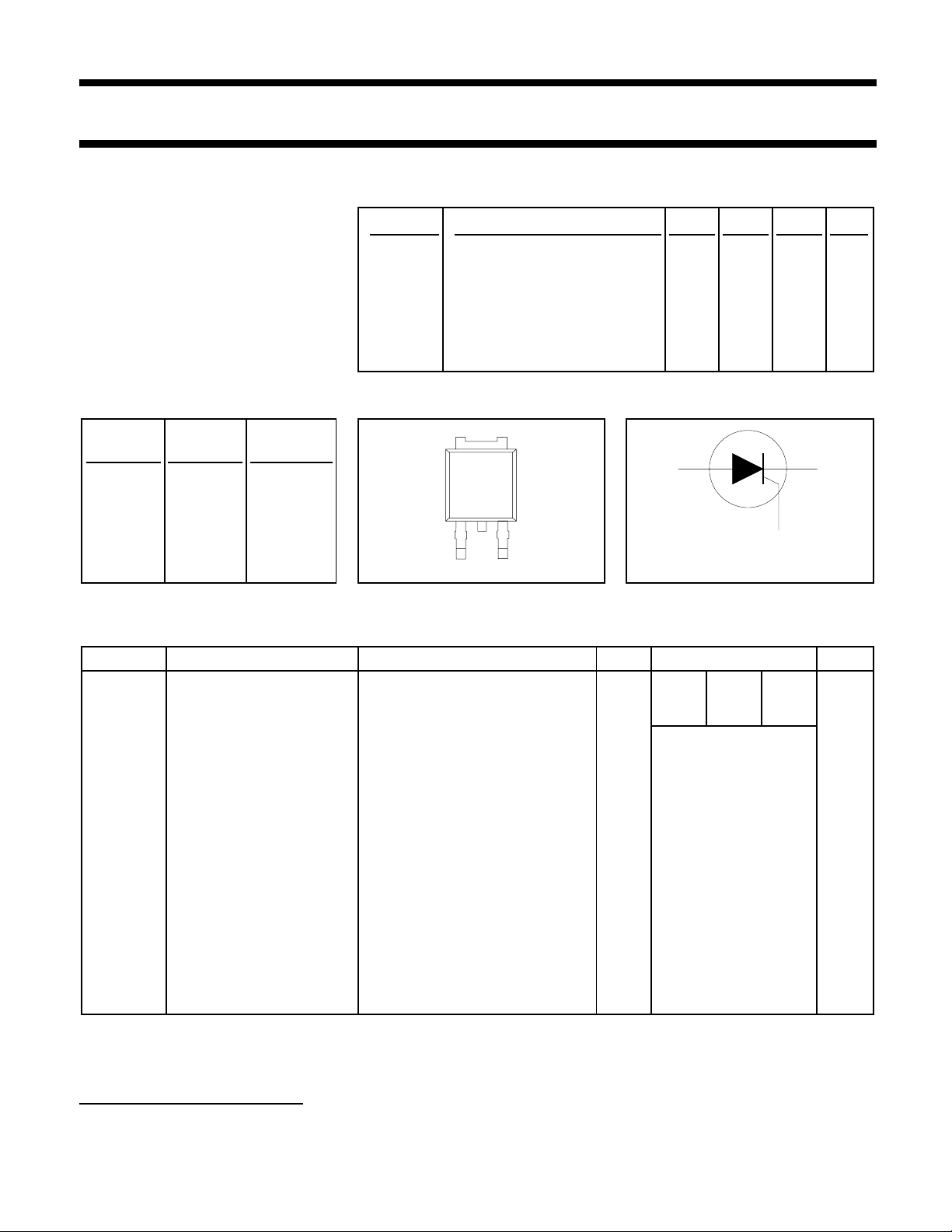
PINNING - SOT428 PIN CONFIGURATION SYMBOL
, Repetitive peak off-state 500 600 800 V
DRM
RRM
T(AV)
T(RMS)
TSM
voltages
Average on-state current 5 5 5 A
RMS on-state current 8 8 8 A
Non-repetitive peak on-state 65 65 65 A
BT300M series
PIN Standard Alternative
tab
NUMBER S M
1 cathode gate
ak
2 anode anode
3 gate cathode
tab anode anode
2
1
3
g
LIMITING VALUES
Limiting values in accordance with the Absolute Maximum System (IEC 134).
SYMBOL PARAMETER CONDITIONS MIN. MAX. UNIT
-500R -600R -800R
V
DRM
, V
Repetitive peak off-state - 5001600
RRM
voltages
I
T(AV)
I
T(RMS)
I
TSM
Average on-state current half sine wave; Tmb ≤ 107 ˚C - 5 A
RMS on-state current all conduction angles - 8 A
Non-repetitive peak half sine wave; Tj = 25 ˚C prior to
on-state current surge
t = 10 ms - 65 A
I2tI
2
t for fusing t = 10 ms - 21 A2s
t = 8.3 ms - 71 A
dIT/dt Repetitive rate of rise of ITM = 10 A; IG = 50 mA; - 50 A/µs
on-state current after dIG/dt = 50 mA/µs
triggering
I
V
V
P
P
T
T
GM
GM
RGM
GM
G(AV)
stg
j
Peak gate current - 2 A
Peak gate voltage - 5 V
Peak reverse gate voltage - 5 V
Peak gate power - 5 W
Average gate power over any 20 ms period - 0.5 W
Storage temperature -40 150 ˚C
Operating junction - 125 ˚C
temperature
1
800 V
1 Although not recommended, off-state voltages up to 800V may be applied without damage, but the thyristor may
switch to the on-state. The rate of rise of current should not exceed 15 A/µs.
September 1997 1 Rev 1.100

Philips Semiconductors Product specification
Thyristors BT300S series
THERMAL RESISTANCES
SYMBOL PARAMETER CONDITIONS MIN. TYP. MAX. UNIT
R
th j-mb
R
th j-a
STATIC CHARACTERISTICS
Tj = 25 ˚C unless otherwise stated
SYMBOL PARAMETER CONDITIONS MIN. TYP. MAX. UNIT
I
GT
I
L
I
H
V
T
V
GT
ID, I
R
Thermal resistance - - 2.2 K/W
junction to mounting base
Thermal resistance pcb (FR4) mounted; footprint as in Fig.14 - 75 - K/W
junction to ambient
Gate trigger current VD = 12 V; IT = 0.1 A - 2 15 mA
Latching current VD = 12 V; IGT = 0.1 A - 10 40 mA
Holding current VD = 12 V; IGT = 0.1 A - 10 20 mA
On-state voltage IT = 12 A - 1.35 1.6 V
Gate trigger voltage VD = 12 V; IT = 0.1 A - 0.6 1.5 V
Off-state leakage current VD = V
VD = V
; IT = 0.1 A; Tj = 125 ˚C 0.25 0.4 - V
DRM(max)
DRM(max)
; VR = V
; Tj = 125 ˚C - 0.1 0.5 mA
RRM(max)
BT300M series
DYNAMIC CHARACTERISTICS
Tj = 25 ˚C unless otherwise stated
SYMBOL PARAMETER CONDITIONS MIN. TYP. MAX. UNIT
dVD/dt Critical rate of rise of VDM = 67% V
off-state voltage exponential waveform.
t
gt
Gate controlled turn-on ITM = 10 A; VD = V
time dIG/dt = 5 A/µs
t
q
Circuit commutated VD = 67% V
turn-off time ITM = 12 A; VR = 25 V; dITM/dt = 30 A/µs;
dVD/dt = 50 V/µs; RGK = 100 Ω
DRM(max)
; Tj = 125 ˚C;
DRM(max)
Gate open circuit 50 100 - V/µs
RGK = 100 Ω 200 1000 - V/µs
; IG = 0.1 A; - 2 - µs
DRM(max)
; Tj = 125 ˚C; - 70 - µs
September 1997 2 Rev 1.100
 Loading...