

Philips Semiconductors Product specification
Thyristors BT258U series
logic level
GENERAL DESCRIPTION QUICK REFERENCE DATA
Passivated, sensitive gate thyristors SYMBOL PARAMETER MAX. MAX. MAX. UNIT
inaplasticenvelope, intended for use
in general purpose switching and BT258U- 500R 600R 800R
phase control applications. These V
devices are intended to be interfaced V
directly to microcontrollers, logic I
integrated circuits and other low I
power gate trigger circuits. I
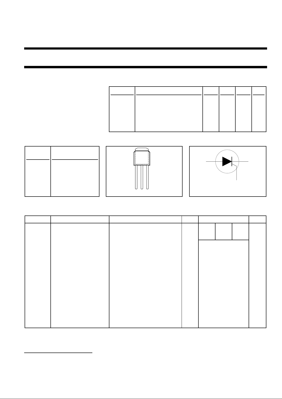
PINNING - SOT533 PIN CONFIGURATION SYMBOL
PIN DESCRIPTION
NUMBER
1 cathode
2 anode
, Repetitive peak off-state 500 600 800 V
DRM
RRM
T(AV)
T(RMS)
TSM
voltages
Average on-state current 5 5 5 A
RMS on-state current 8 8 8 A
Non-repetitive peak on-state 75 75 75 A
current
ak
3 gate
tab anode
Top view
1
23
MBK915
g
LIMITING VALUES
Limiting values in accordance with the Absolute Maximum System (IEC 134).
SYMBOL PARAMETER CONDITIONS MIN. MAX. UNIT
V
DRM
I
T(AV)
I
T(RMS)
I
TSM
, V
Repetitive peak off-state - 5001600
RRM
voltages
Average on-state current half sine wave; Tmb ≤ 111 ˚C - 5 A
RMS on-state current all conduction angles - 8 A
Non-repetitive peak half sine wave; Tj = 25 ˚C prior to
on-state current surge
t = 10 ms - 75 A
-500R -600R -800R
I2tI
2
t for fusing t = 10 ms - 28 A2s
t = 8.3 ms - 82 A
dIT/dt Repetitive rate of rise of ITM = 10 A; IG = 50 mA; - 50 A/µs
on-state current after dIG/dt = 50 mA/µs
triggering
I
V
V
P
P
T
T
GM
GM
RGM
GM
G(AV)
stg
j
Peak gate current - 2 A
Peak gate voltage - 5 V
Peak reverse gate voltage - 5 V
Peak gate power - 5 W
Average gate power over any 20 ms period - 0.5 W
Storage temperature -40 150 ˚C
Operating junction - 125
temperature
1
2
800 V
˚C
1 Although not recommended, off-state voltages up to 800V may be applied without damage, but the thyristor may
switch to the on-state. The rate of rise of current should not exceed 15 A/µs.
2 Note: Operation above 110˚C may require the use of a gate to cathode resistor of 1kΩ or less.
March 1999 1 Rev 1.000

Philips Semiconductors Product specification
Thyristors BT258U series
logic level
THERMAL RESISTANCES
SYMBOL PARAMETER CONDITIONS MIN. TYP. MAX. UNIT
R
th j-mb
R
th j-a
STATIC CHARACTERISTICS
Tj = 25 ˚C unless otherwise stated
SYMBOL PARAMETER CONDITIONS MIN. TYP. MAX. UNIT
I
GT
I
L
I
H
V
T
V
GT
ID, I
R
Thermal resistance - - 2.0 K/W
junction to mounting base
Thermal resistance in free air - 70 - K/W
junction to ambient
Gate trigger current VD = 12 V; IT = 0.1 A - 50 200 µA
Latching current VD = 12 V; IGT = 0.1 A - 0.4 10 mA
Holding current VD = 12 V; IGT = 0.1 A - 0.3 6 mA
On-state voltage IT = 16 A - 1.3 1.5 V
Gate trigger voltage VD = 12 V; IT = 0.1 A - 0.4 1.5 V
Off-state leakage current VD = V
VD = V
; IT = 0.1 A; Tj = 110 ˚C 0.1 0.2 - V
DRM(max)
DRM(max)
; VR = V
; Tj = 125 ˚C - 0.1 0.5 mA
RRM(max)
DYNAMIC CHARACTERISTICS
Tj = 25 ˚C unless otherwise stated
SYMBOL PARAMETER CONDITIONS MIN. TYP. MAX. UNIT
dVD/dt Critical rate of rise of VDM = 67% V
off-state voltage exponential waveform; RGK = 100 Ω
t
gt
t
q
Gate controlled turn-on ITM = 10 A; VD = V
time dIG/dt = 0.2 A/µs
Circuit commutated VD = 67% V
turn-off time ITM = 12 A; VR = 24 V; dITM/dt = 10 A/µs;
dVD/dt = 2 V/µs; RGK = 1 kΩ
DRM(max)
; Tj = 125 ˚C; 50 100 - V/µs
DRM(max)
; IG = 5 mA; - 2 - µs
DRM(max)
; Tj = 125 ˚C; - 100 - µs
March 1999 2 Rev 1.000
 Loading...