

Philips BT169GW, BT169EW, BT169BW Datasheet
Philips Semiconductors Product specification
Thyristor BT169W Series
logic level
GENERAL DESCRIPTION QUICK REFERENCE DATA
Passivated, sensitive gate thyristor in SYMBOL PARAMETER MAX. MAX. MAX. MAX. UNIT
a plastic envelope, suitable for
surface mounting, intended for use in BT169 BW DW EW GW
generalpurposeswitchingandphase V
control applications. This device is V
intended to be interfaced directly to I
microcontrollers, logic integrated current
circuits and other low power gate I
trigger circuits. I
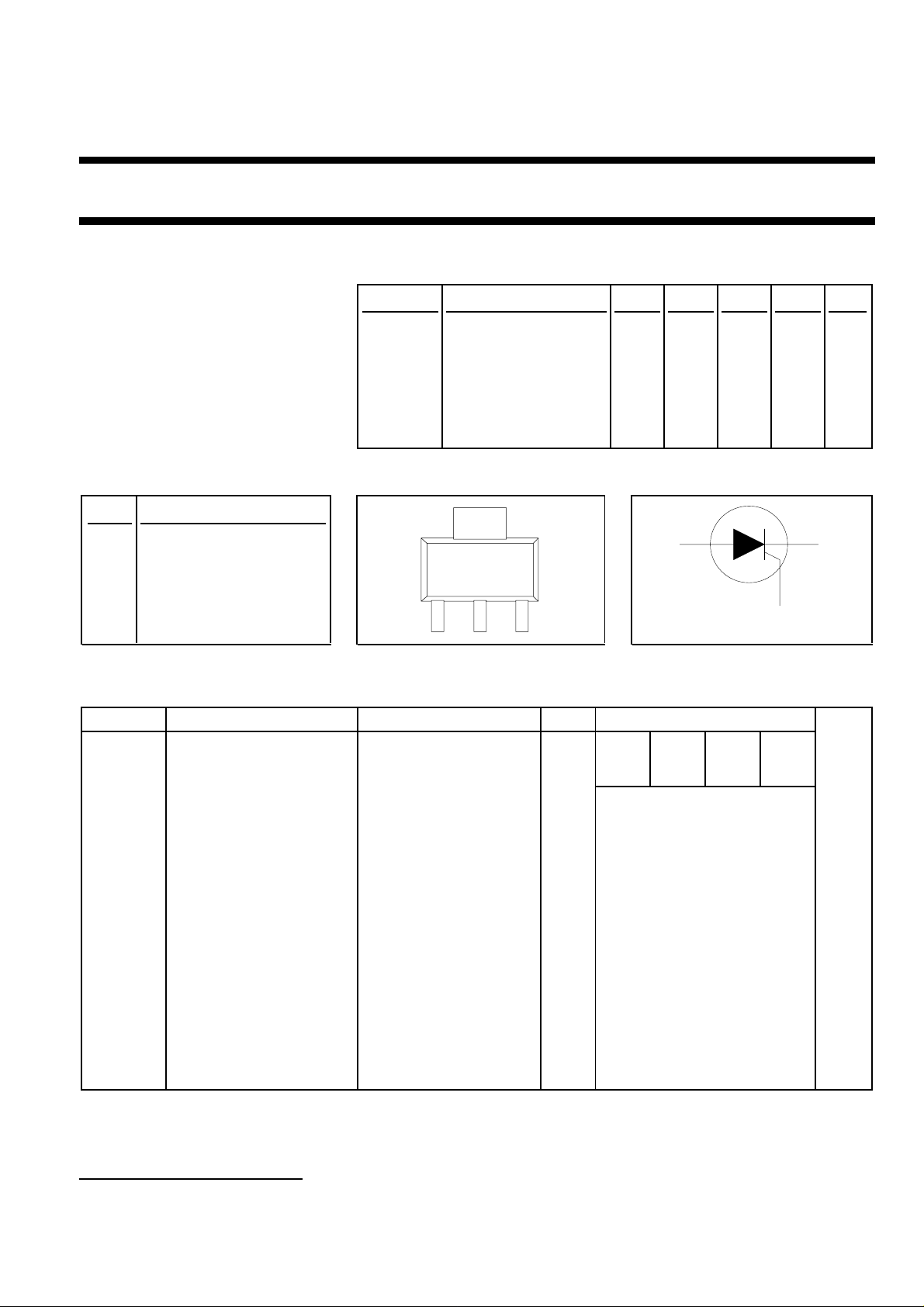
PINNING - SOT223 PIN CONFIGURATION SYMBOL
, Repetitive peak 200 400 500 600 V
DRM
RRM
T(AV)
T(RMS)
TSM
off-state voltages
Average on-state 0.5 0.5 0.5 0.5 A
RMS on-state current 0.8 0.8 0.8 0.8 A
Non-repetitive peak 8888A
on-state current
PIN DESCRIPTION
1 cathode
4
ak
2 anode
3 gate
tab anode
1
23
g
LIMITING VALUES
Limiting values in accordance with the Absolute Maximum System (IEC 134).
SYMBOL PARAMETER CONDITIONS MIN. MAX. UNIT
V
I
T(AV)
DRM
, V
Repetitive peak off-state - 200140015001600
RRM
voltages
Average on-state current half sine wave; - 0.63 A
Tsp ≤ 112 ˚C
BDEG
I
T(RMS)
I
TSM
RMS on-state current all conduction angles - 1 A
Non-repetitive peak half sine wave;
on-state current Tj = 25 ˚C prior to surge
t = 10 ms - 8 A
I2tI
2
t for fusing t = 10 ms - 0.32 A2s
t = 8.3 ms - 9 A
dIT/dt Repetitive rate of rise of ITM = 2 A; IG = 10 mA; - 50 A/µs
on-state current after dIG/dt = 100 mA/µs
triggering
I
V
V
P
P
T
T
GM
GM
RGM
GM
G(AV)
stg
j
Peak gate current - 1 A
Peak gate voltage - 5 V
Peak reverse gate voltage - 5 V
Peak gate power - 2 W
Average gate power over any 20 ms period - 0.1 W
Storage temperature -40 150 ˚C
Operating junction - 125 ˚C
temperature
1
V
1 Although not recommended, off-state voltages up to 800V may be applied without damage, but the thyristor may
switch to the on-state. The rate of rise of current should not exceed 15 A/µs.
September 2001 1 Rev 1.400

Philips Semiconductors Product specification
Thyristor BT169W Series
logic level
THERMAL RESISTANCES
SYMBOL PARAMETER CONDITIONS MIN. TYP. MAX. UNIT
R
th j-sp
R
th j-a
STATIC CHARACTERISTICS
Tj = 25 ˚C unless otherwise stated
SYMBOL PARAMETER CONDITIONS MIN. TYP. MAX. UNIT
I
GT
I
L
I
H
V
T
V
GT
ID, I
R
Thermal resistance - - 15 K/W
junction to solder point
Thermal resistance pcb mounted, minimum footprint - 156 - K/W
junction to ambient pcb mounted; pad area as in fig:14 - 70 - K/W
Gate trigger current VD = 12 V; IT = 10 mA; gate open circuit - 50 200 µA
Latching current VD = 12 V; IGT = 0.5 mA; RGK = 1 kΩ -26mA
Holding current VD = 12 V; IGT = 0.5 mA; RGK = 1 kΩ -25mA
On-state voltage IT = 2 A - 1.35 1.5 V
Gate trigger voltage VD = 12 V; IT = 10 mA; gate open circuit - 0.5 0.8 V
VD = V
gate open circuit
Off-state leakage current VD = V
; IT = 10 mA; Tj = 125 ˚C; 0.2 0.3 - V
DRM(max)
DRM(max)
; VR = V
; Tj = 125 ˚C; - 0.05 0.1 mA
RRM(max)
RGK = 1 kΩ
DYNAMIC CHARACTERISTICS
Tj = 25 ˚C unless otherwise stated
SYMBOL PARAMETER CONDITIONS MIN. TYP. MAX. UNIT
dVD/dt Critical rate of rise of VDM =67% V
off-state voltage exponential waveform; RGK = 1k Ω
t
gt
Gate controlled turn-on ITM = 2 A; VD = V
time dIG/dt = 0.1 A/µs
t
q
Circuit commutated VD = 67% V
turn-off time ITM = 1.6 A; VR = 35 V; dITM/dt = 30 A/µs;
dVD/dt = 2 V/µs; RGK = 1 kΩ
DRM(max)
; Tj = 125 ˚C; 500 800 - V/µs
DRM(max)
; IG = 10 mA; - 2 - µs
DRM(max)
; Tj = 125 ˚C; - 100 - µs
September 2001 2 Rev 1.400
 Loading...