

Philips BT169E, BT169D Datasheet
Philips Semiconductors Product specification
Thyristors BT169 series
logic level
GENERAL DESCRIPTION QUICK REFERENCE DATA
Glass passivated, sensitive gate SYMBOL PARAMETER MAX. MAX. MAX. MAX. UNIT
thyristors in a plastic envelope,
intended for use in general purpose BT169 B D E G
switching and phase control V
DRM
, Repetitive peak 200 400 500 600 V
applications. These devices are V
RRM
off-state voltages
intended to be interfaced directly to I
T(AV)
Average on-state 0.5 0.5 0.5 0.5 A
microcontrollers, logic integrated current
circuits and other low power gate I
T(RMS)
RMS on-state current 0.8 0.8 0.8 0.8 A
trigger circuits. I
TSM
Non-repetitive peak 8888A
on-state current
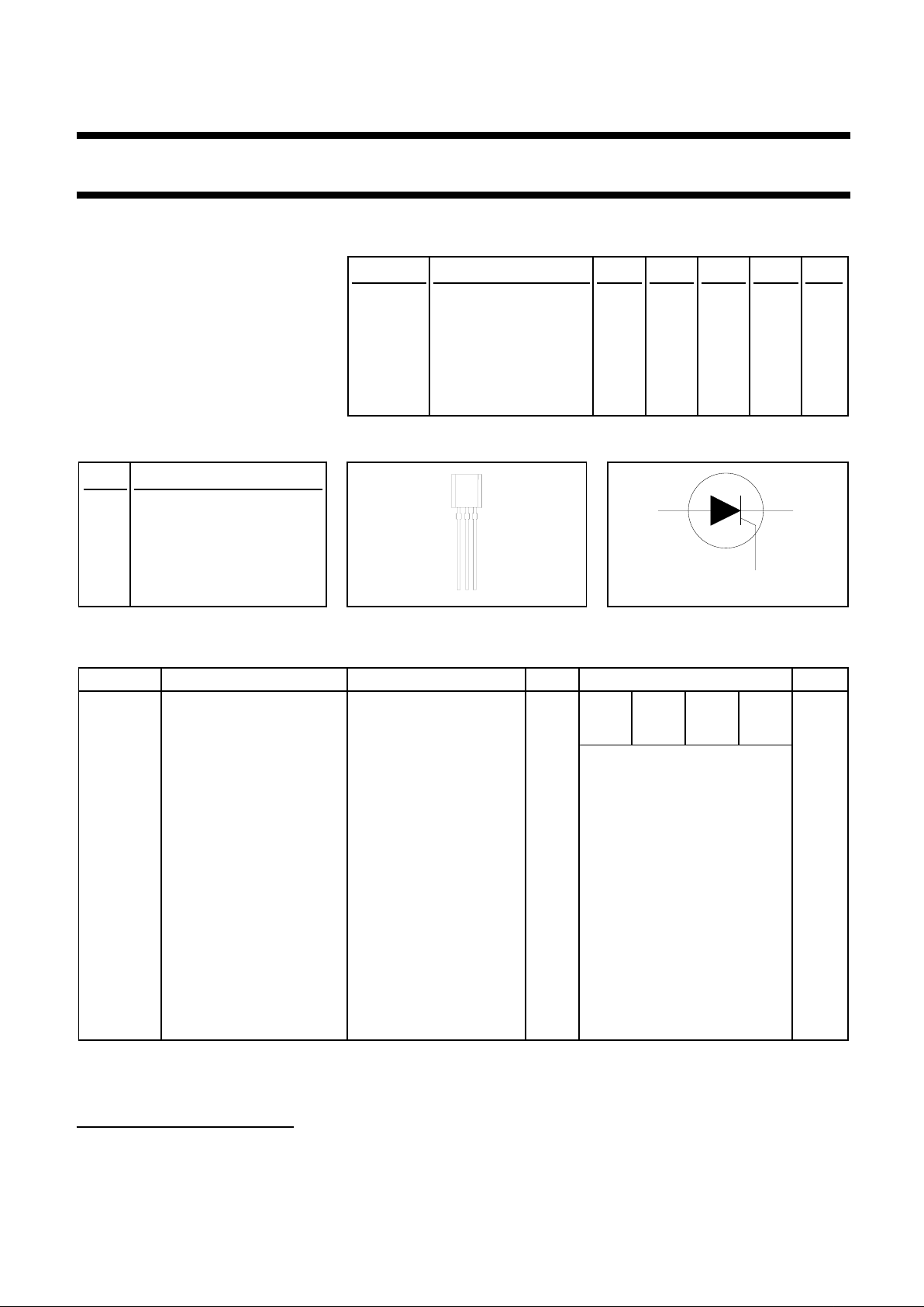
PINNING - TO92 variant PIN CONFIGURATION SYMBOL
PIN DESCRIPTION
1 anode
2 gate
3 cathode
LIMITING VALUES
Limiting values in accordance with the Absolute Maximum System (IEC 134).
SYMBOL PARAMETER CONDITIONS MIN. MAX. UNIT
BDEG
V
DRM
, V
RRM
Repetitive peak off-state - 200140015001600
1
V
voltages
I
T(AV)
Average on-state current half sine wave; - 0.5 A
T
lead
≤ 83 ˚C
I
T(RMS)
RMS on-state current all conduction angles - 0.8 A
I
TSM
Non-repetitive peak t = 10 ms - 8 A
on-state current t = 8.3 ms - 9 A
half sine wave;
Tj = 25 ˚C prior to surge
I2tI
2
t for fusing t = 10 ms - 0.32 A2s
dIT/dt Repetitive rate of rise of ITM = 2 A; IG = 10 mA; - 50 A/µs
on-state current after dIG/dt = 100 mA/µs
triggering
I
GM
Peak gate current - 1 A
V
GM
Peak gate voltage - 5 V
V
RGM
Peak reverse gate voltage - 5 V
P
GM
Peak gate power - 2 W
P
G(AV)
Average gate power over any 20 ms period - 0.1 W
T
stg
Storage temperature -40 150 ˚C
T
j
Operating junction - 125 ˚C
temperature
ak
g
321
1 Although not recommended, off-state voltages up to 800V may be applied without damage, but the thyristor may
switch to the on-state. The rate of rise of current should not exceed 15 A/µs.
September 1997 1 Rev 1.200

Philips Semiconductors Product specification
Thyristors BT169 series
logic level
THERMAL RESISTANCES
SYMBOL PARAMETER CONDITIONS MIN. TYP. MAX. UNIT
R
th j-lead
Thermal resistance - - 60 K/W
junction to lead
R
th j-a
Thermal resistance pcb mounted; lead length = 4mm - 150 - K/W
junction to ambient
STATIC CHARACTERISTICS
Tj = 25 ˚C unless otherwise stated
SYMBOL PARAMETER CONDITIONS MIN. TYP. MAX. UNIT
I
GT
Gate trigger current VD = 12 V; IT = 10 mA; gate open circuit - 50 200 µA
I
L
Latching current VD = 12 V; IGT = 0.5 mA; RGK = 1 kΩ -26mA
I
H
Holding current VD = 12 V; IGT = 0.5 mA; RGK = 1 kΩ -25mA
V
T
On-state voltage IT = 1 A - 1.2 1.35 V
V
GT
Gate trigger voltage VD = 12 V; IT = 10 mA; gate open circuit - 0.5 0.8 V
VD = V
DRM(max)
; IT = 10 mA; Tj = 125 ˚C; 0.2 0.3 - V
gate open circuit
ID, I
R
Off-state leakage current VD = V
DRM(max)
; VR = V
RRM(max)
; Tj = 125 ˚C; - 0.05 0.1 mA
RGK = 1 kΩ
DYNAMIC CHARACTERISTICS
Tj = 25 ˚C unless otherwise stated
SYMBOL PARAMETER CONDITIONS MIN. TYP. MAX. UNIT
dVD/dt Critical rate of rise of VDM = 67% V
DRM(max)
; Tj = 125 ˚C; - 25 - V/µs
off-state voltage exponential waveform; RGK = 1 kΩ
t
gt
Gate controlled turn-on ITM = 2 A; VD = V
DRM(max)
; IG = 10 mA; - 2 - µs
time dIG/dt = 0.1 A/µs
t
q
Circuit commutated VD = 67% V
DRM(max)
; Tj = 125 ˚C; - 100 - µs
turn-off time ITM = 1.6 A; VR = 35 V; dITM/dt = 30 A/µs;
dVD/dt = 2 V/µs; RGK = 1 kΩ
September 1997 2 Rev 1.200
 Loading...