

Philips BT168G, BT168E, BT168D, BT168B Datasheet
Philips Semiconductors Product specification
Thyristors BT168 series
logic level for RCD/ GFI/ LCCB applications
GENERAL DESCRIPTION QUICK REFERENCE DATA
Glass passivated, sensitive gate SYMBOL PARAMETER MAX. MAX. MAX. MAX. UNIT
thyristors in a plastic envelope,
intended for use in Residual Current BT168 B D E G
Devices/ Ground Fault Interrupters/ V
Leakage Current Circuit Breakers V
(RCD/ GFI/ LCCB) applications I
where a minimum IGTlimit is needed. current
These devices may be interfaced I
directly to microcontrollers, logic I
integrated circuits and other low on-state current
power gate trigger circuits.
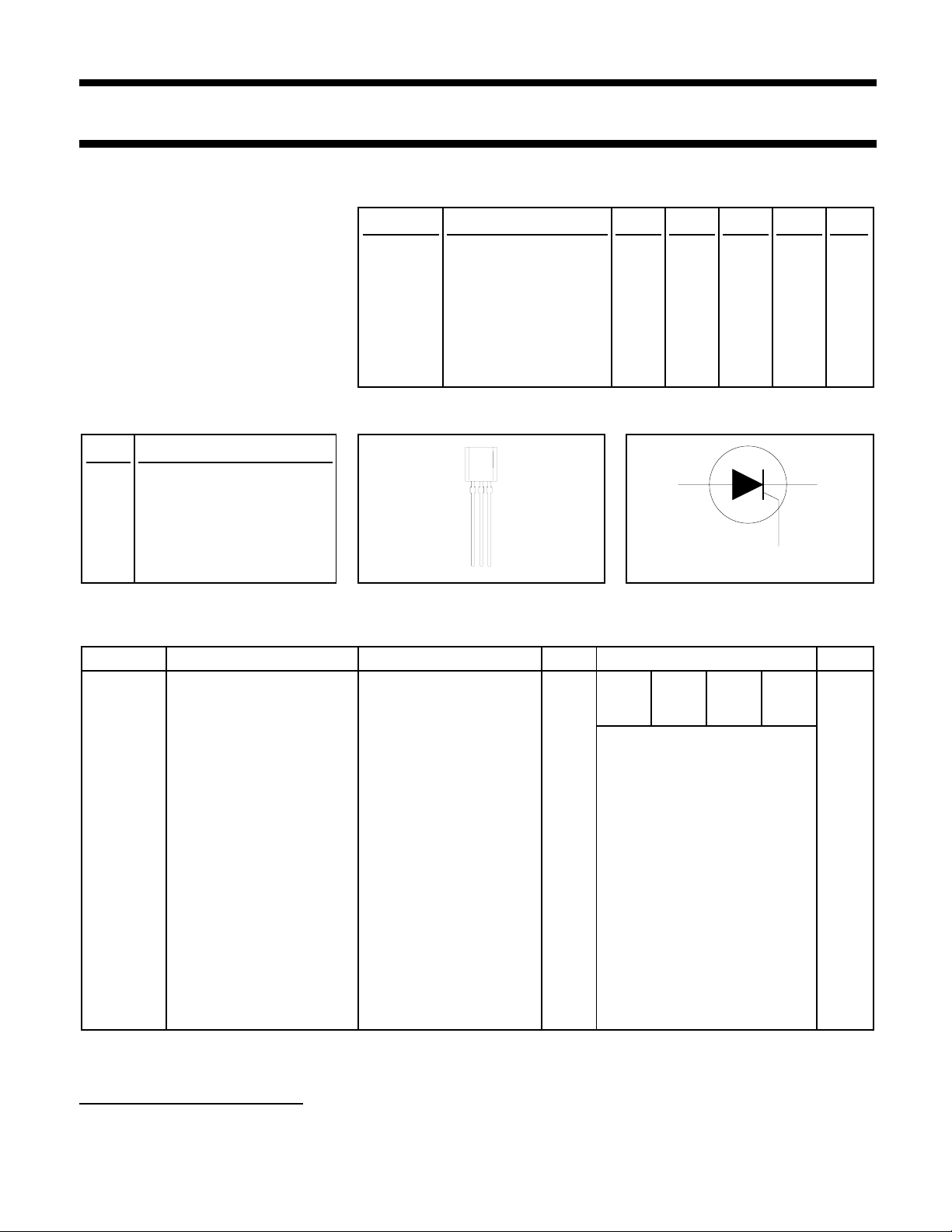
PINNING - TO92 variant PIN CONFIGURATION SYMBOL
PIN DESCRIPTION
, Repetitive peak 200 400 500 600 V
DRM
RRM
T(AV)
T(RMS)
TSM
off-state voltages
Average on-state 0.5 0.5 0.5 0.5 A
RMS on-state current 0.8 0.8 0.8 0.8 A
Non-repetitive peak 8888A
1 anode
ak
2 gate
3 cathode
321
g
LIMITING VALUES
Limiting values in accordance with the Absolute Maximum System (IEC 134).
SYMBOL PARAMETER CONDITIONS MIN. MAX. UNIT
BDEG
V
DRM
, V
Repetitive peak off-state - 200140015001600
RRM
voltages
I
T(AV)
I
T(RMS)
I
TSM
Average on-state current half sine wave; - 0.5 A
T
≤ 83 ˚C
RMS on-state current all conduction angles - 0.8 A
lead
Non-repetitive peak t = 10 ms - 8 A
on-state current t = 8.3 ms - 9 A
half sine wave;
I2tI
2
t for fusing t = 10 ms - 0.32 A2s
Tj = 25 ˚C prior to surge
dIT/dt Repetitive rate of rise of ITM = 2 A; IG = 10 mA; - 50 A/µs
on-state current after dIG/dt = 100 mA/µs
triggering
I
V
V
P
P
T
T
GM
GM
RGM
GM
G(AV)
stg
j
Peak gate current - 1 A
Peak gate voltage - 5 V
Peak reverse gate voltage - 5 V
Peak gate power - 2 W
Average gate power over any 20 ms period - 0.1 W
Storage temperature -40 150 ˚C
Operating junction - 125 ˚C
temperature
1
V
1 Although not recommended, off-state voltages up to 800V may be applied without damage, but the thyristor may
switch to the on-state. The rate of rise of current should not exceed 15 A/µs.
September 1997 1 Rev 1.100

Philips Semiconductors Product specification
Thyristors BT168 series
logic level for RCD/ GFI/ LCCB Applications
THERMAL RESISTANCES
SYMBOL PARAMETER CONDITIONS MIN. TYP. MAX. UNIT
R
th j-lead
R
th j-a
STATIC CHARACTERISTICS
Tj = 25 ˚C unless otherwise stated
SYMBOL PARAMETER CONDITIONS MIN. TYP. MAX. UNIT
I
GT
I
L
I
H
V
T
V
GT
ID, I
R
Thermal resistance - - 60 K/W
junction to lead
Thermal resistance pcb mounted; lead length = 4mm - 150 - K/W
junction to ambient
Gate trigger current VD = 12 V; IT = 10 mA; gate open circuit 20 50 200 µA
Latching current VD = 12 V; IGT = 0.5 mA; RGK = 1 kΩ -26mA
Holding current VD = 12 V; IGT = 0.5 mA; RGK = 1 kΩ -25mA
On-state voltage IT = 1 A - 1.2 1.35 V
Gate trigger voltage VD = 12 V; IT = 10 mA; gate open circuit - 0.5 0.8 V
VD = V
; IT = 10 mA; Tj = 125 ˚C; 0.2 0.3 - V
DRM(max)
gate open circuit
Off-state leakage current VD = V
RGK = 1 kΩ
DRM(max)
; VR = V
; Tj = 125 ˚C; - 0.05 0.1 mA
RRM(max)
DYNAMIC CHARACTERISTICS
Tj = 25 ˚C unless otherwise stated
SYMBOL PARAMETER CONDITIONS MIN. TYP. MAX. UNIT
dVD/dt Critical rate of rise of VDM = 67% V
off-state voltage exponential waveform; RGK = 1 kΩ
t
gt
t
q
Gate controlled turn-on ITM = 2 A; VD = V
time dIG/dt = 0.1 A/µs
Circuit commutated VD = 67% V
turn-off time ITM = 1.6 A; VR = 35 V; dITM/dt = 30 A/µs;
dVD/dt = 2 V/µs; RGK = 1 kΩ
DRM(max)
; Tj = 125 ˚C; - 25 - V/µs
DRM(max)
; IG = 10 mA; - 2 - µs
DRM(max)
; Tj = 125 ˚C; - 100 - µs
September 1997 2 Rev 1.100
 Loading...