

Philips blf861a DATASHEETS

DISCRETE SEMICONDUCTORS
M3D392
DATA SHEET
BLF861A
UHF power LDMOS transistor
Preliminary specification 2000 Aug 04
Philips Semiconductors Preliminary specification
UHF power LDMOS transistor BLF861A
FEATURES
• High power gain
• Easy power control
• Excellent ruggedness
• Designed to withstand abrupt load mismatch errors
• Source on underside eliminates DC isolators; reducing
common mode inductance
• Designed for broadband operation (UHF band)
• Internal input and output matching for high gain and
optimum broadband operation.
APPLICATIONS
• Communication transmitter applications in the UHF
frequency range.
DESCRIPTION
Silicon N-channel enhancement mode lateral D-MOS
push-pull transistor in a SOT540A package with ceramic
cap. The common source is connected to the mounting
flange.
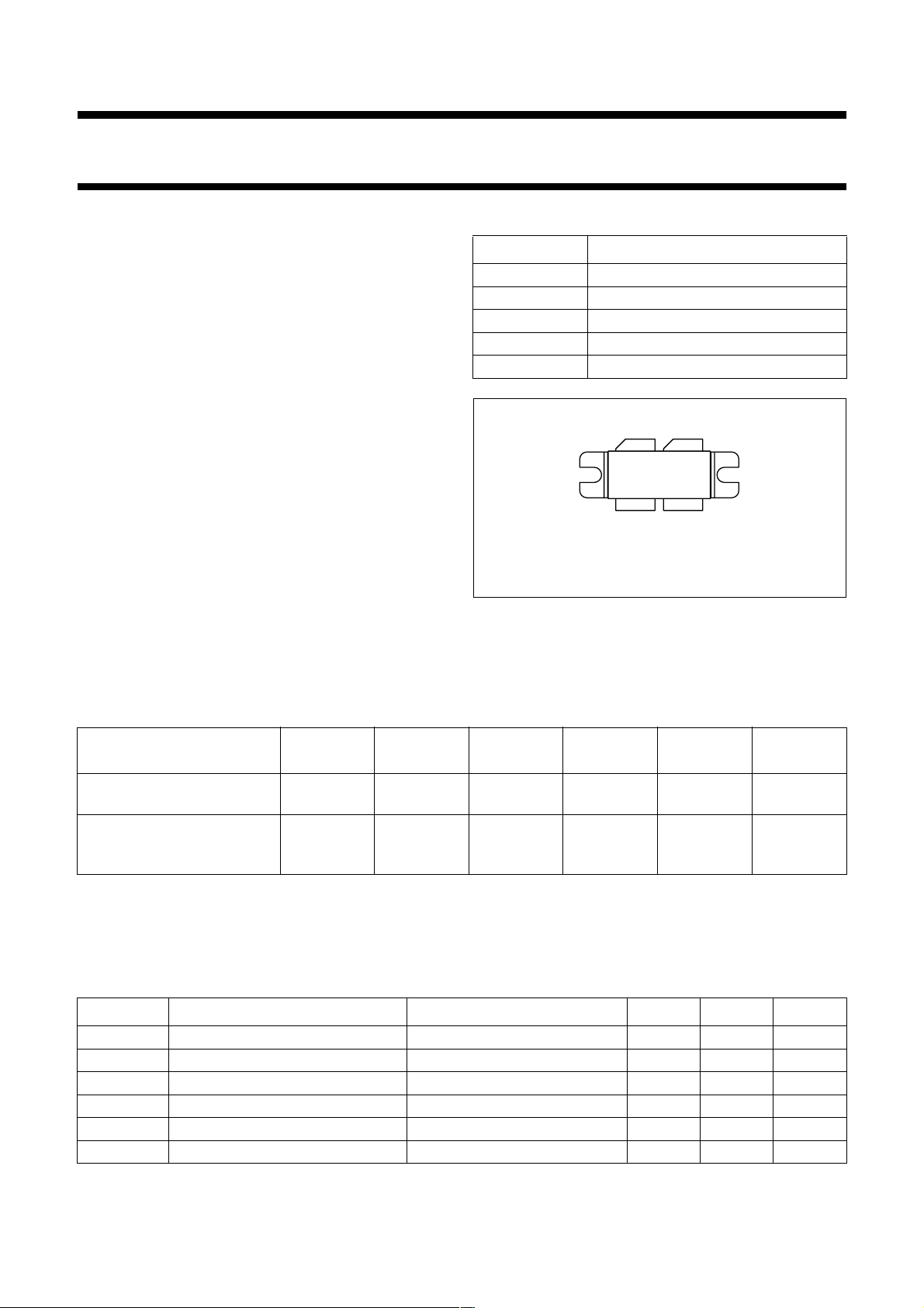
PINNING - SOT540A
PIN DESCRIPTION
1drain1
2drain2
3gate1
4gate2
5 source connected to flange
12
Top view
Fig.1 Simplified outline.
5
43
MBK777
QUICK REFERENCE DATA
RF performance at T
MODE OF OPERATION
CW, class-AB 860 32 150 >13.5
=25°C in a common source 860 MHz test circuit.
h
f
(MHz)
V
(V)
DS
P
(W)
L
G
p
(dB)
η
(%)
D
>50 ≤1
typ. 14.5
PAL BG (TV); class-AB 860 (ch 69) 32 >150
>14 >40 note 1
typ. 170
(peak sync)
Note
1. Sync compression: input sync ≥ 33%; output sync 27%.
LIMITING VALUES
In accordance with the Absolute Maximum Rating System (IEC 60134).
SYMBOL PARAMETER CONDITIONS MIN. MAX. UNIT
V
DS
V
GS
I
D
P
tot
T
stg
T
j
drain-source voltage − 65 V
gate-source voltage −±15 V
drain current (DC) − 18 A
total power dissipation Tmb≤ 25 °C − 318 W
storage temperature −65 +150 °C
junction temperature − 200 °C
∆G
(dB)
p
2000 Aug 04 2

Philips Semiconductors Preliminary specification
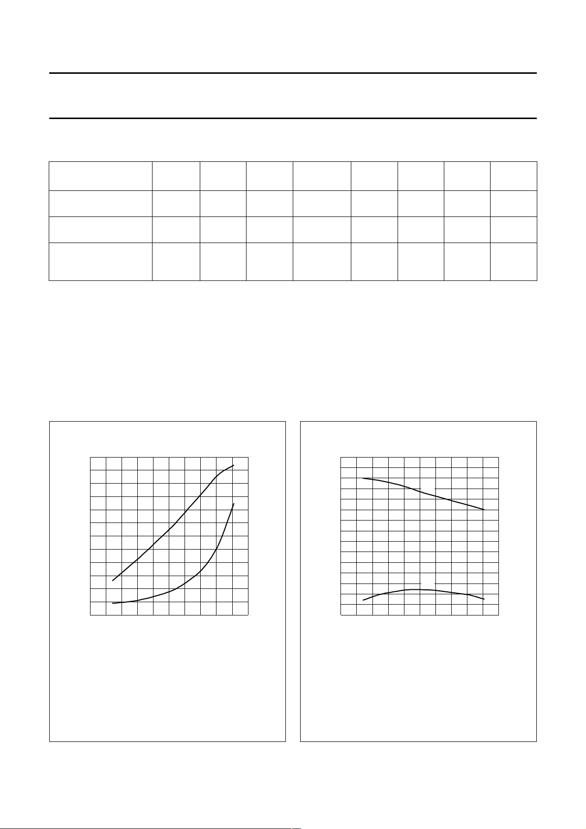
Fig.2 Output capacitance as a function of
drain-source voltage; typical values per
section.
VGS=0; f=1MHz; Tj=25°C.
UHF power LDMOS transistor BLF861A
THERMAL CHARACTERISTICS
SYMBOL PARAMETER CONDITIONS VALUE UNIT
R
th j-mb
R
th mb-h
CHARACTERISTICS
=25°C; per section; unless otherwise specified.
T
j
SYMBOL PARAMETER CONDITIONS MIN. TYP. MAX. UNIT
V
(BR)DSS
V
GSth
I
DSS
I
DSX
I
GSS
g
fs
R
DSon
C
iss
C
oss
C
rss
thermal resistance from junction to mounting base Tmb=25°C; P
= 318 W 0.55 K/W
tot
thermal resistance from mounting base to heatsink 0.2 K/W
drain-source breakdown voltage VGS=0; ID=1.5mA 65 −−V
gate-source threshold voltage VDS=10V; ID= 150 mA 4 − 5.5 V
drain-source leakage current VGS=0; VDS=32V −−2.2 µA
drain cut-off current VGS=V
+9V; VDS=10V 18 −−A
GSth
gate leakage current VGS= ±15 V; VDS=0 −−25 nA
forward transconductance VDS=10V; ID=4A − 4 − S
drain-source on-state resistance VGS=V
input capacitance VGS=0; VDS=32V; f=1MHz
output capacitance VGS=0; VDS=32V; f=1MHz
feedback capacitance VGS=0; VDS=32V; f=1MHz
+9V; ID=4A − 160 − mΩ
GSth
(1)
− 82 − pF
(1)
− 40 − pF
(1)
− 6 − pF
Note
1. Capacitance values without internal matching.
100
C
oss
(pF)
80
60
40
20
0
0 1020304050
V
(V)
DS
2000 Aug 04 3
Philips Semiconductors Preliminary specification
handbook, halfpage
400 900
12
0
4
8
500
x
i
r
i
Z
i
(Ω)
f (MHz)
600 700 800
MCD871
Fig.3 Input impedance as a function of frequency
(series components); typical push-pull
values.
CW, class-AB operation; VDS=32V; IDQ=1A;
P
L
= 170 W (total device); Th=25°C.
UHF power LDMOS transistor BLF861A
APPLICATION INFORMATION
RF performance in a common source 860 MHz test circuit. T
=25°C; R
h
= 0.15 K/W; unless otherwise specified.
th mb-h
MODE OF
OPERATION
CW; class-AB 860 32 1 150 >13.5
f
(MHz)
V
(V)
DS
I
DQ
(A)
P
(W)
L
G
p
(dB)
η
(%)
D
d
Im
(dBc)
∆G
(dB)
p
>50 −≤1
typ. 14.5
2-tone; class-AB f
PAL BG (TV); class-AB 860
= 860
1
f
= 860.1
1
(ch 69)
32 1 150 (PEP) >14 >40 ≤−25 −
32 1 > 150
>14 >40 − note 1
typ. 170
(peak sync)
Note
1. Sync compression: input sync ≥ 33%; output sync 27% measured in 860 MHz test circuit.
Ruggedness in class-AB operation
The BLF861A is capable of withstanding a load mismatch corresponding to VSWR = 10 : 1 through all phases under the
following conditions: V
= 32 V; f = 860 MHz at rated load power.
DS
The BLF861A is an improved version of the BLF861 on ruggedness and is capable to withstand abrupt source or load
mismatch errors under the nominal power condition.
10
handbook, halfpage
Z
L
(Ω)
R
L
MCD872
2000 Aug 04 4
5
0
X
L
−5
400 900
CW, class-AB operation; VDS=32V; IDQ=1A;
= 170 W (total device); Th=25°C.
P
L
500 600 700 800
f (MHz)
Fig.4 Load impedance as a function of frequency
(series components); typical push-pull
values.
 Loading...